


Racal RA-117
Radio Receiver

1. Contents
1. Contents . . . . . . . . . . . . . . . . . . . . . . . . . . . . . 2
2. List of Illustrations . . . . . . . . . . . . . . . . . . . . . . . . 3
3. Technical Specification . . . . . . . . . . . . . . . . . . . . . . 4
4. Introduction . . . . . . . . . . . . . . . . . . . . . . . . . . . 7
5. Installation . . . . . . . . . . . . . . . . . . . . . . . . . . . . 8
6. Operation . . . . . . . . . . . . . . . . . . . . . . . . . . . . 10
7. Brief Technical Description . . . . . . . . . . . . . . . . . . . 14
8. Detailed Circuit Description . . . . . . . . . . . . . . . . . . . 16
9. Maintenance . . . . . . . . . . . . . . . . . . . . . . . . . . . 25
10. Spurious Responses . . . . . . . . . . . . . . . . . . . . . . . 26
11. Fault Diagnosis . . . . . . . . . . . . . . . . . . . . . . . . . 28
12. Representative Test Data . . . . . . . . . . . . . . . . . . . . 30
13. General Servicing and Aligment Procedures . . . . . . . . . . 32
13.1. General Servicing . . . . . . . . . . . . . . . . . . . . . . 33
13.2. Receiver Tests . . . . . . . . . . . . . . . . . . . . . . . . 33
14. Alignment Procedures . . . . . . . . . . . . . . . . . . . . . 37
14.1. Introduction . . . . . . . . . . . . . . . . . . . . . . . . 37
14.2. 100 kc/s I.F. Amplifier . . . . . . . . . . . . . . . . . . . . 37
14.3. 100 kc/s (L-C) Filter . . . . . . . . . . . . . . . . . . . . . 37
14.4. Second V.F.O. . . . . . . . . . . . . . . . . . . . . . . . 39
15. Dismantling . . . . . . . . . . . . . . . . . . . . . . . . . . . 44
16. Component List 1. . . . . . . . . . . . . . . . . . . . . . . . 49
17. Component List 2 . . . . . . . . . . . . . . . . . . . . . . . . 63
18. Valve Data . . . . . . . . . . . . . . . . . . . . . . . . . . . 67
19. Illustrations . . . . . . . . . . . . . . . . . . . . . . . . . . . 69
[2]

2. List of Illustrations
Fig.
Rear View of Receiver Chassis 1
Front Panel, RA.117 2
RA.117 Block Diagram 3
Simplified Balancing Circuit 4
Noise Limiter Circuit 5
Typical Selectivity Curves 6
Terminal Tag Strip 7
Top View of Receiver 8
First V.F.O. - top view 9
First V.F.O. - underside 10
Second V.F.O. 11
1.7 Mc/s Oscillator/Amplifier and Mixer Unit 12
B.F.O. Unit 13
Crystal Calibrator Unit 14
Key to Under-chassis Layout 15
R.F. Attenuator 16
Supply Filters 17
Crystal Oscillator/Amplifier and Harmonic Filter System 18
Second Mixer 19
Band-Pass Filter 20
100 Kc/s I.F. amplifier - right side 21
100 Kc/s I.F. amplifier - left side 22
Power Supply and Audio Stages 23
[3]

3. Technical Specification
Frequency range: 1 – 30 Mc/s
Stability: Afterwarm-up, overall drift is less than 50 c/s per hour
under conditions of constant supply voltage and ambient
temperature.
Input impedance: (1) Wideband 2000-ohms approx.
(2) Wideband 75 ohms.
(3) 5 double-tuned circuits, 75 ohms.
(a) 1 – 2 Mc/s
(b) 2 – 4 Mc/s
(c) 4 – 8 Mc/s
(d) 8 – 16 Mc/s
(e) 16 – 30 Mc/s
Tuning: Effective scale lenght of approximately 145 feet, i.e. 6
inches of scale lenght corresponds to 100 kc/s Frequency
increments remain constant over the entire range.
Calibration: A 100 kc/s signal derived from a 1 Mc/s crystal oscillator
having an accuracy of 5 parts in 106provides check points
at 100 kc/s intervals.
Sensitivity: A1 reception, bandwidth 3 Kc/s; 1µV for 18dB signal-to-
noise ratio. A2 reception, 30% modulated, bandwidth 3
Kc/s; 3µV for 18dB signal-to-noise ratio.
Intermodulation: More than 100dB down for interfering signals at least
10% removed from the wanted signal.
Cross modulation: For wanted signal levels between 3µV and 1mV, an inter-
fering signal 10 Kc/s removed and modulated 30% must
have a level greater than 50dB above that of the wanted
signal to produce a cross modulation of 3%. The ratio
of wanted to unwanted signal is improved up to 10% off
tune, at the rate of 3dB per cent.
Blocking: With similar conditions to those for cross modulation an
unwanted signal f2must be 60dB greater before the audio
output of the wanted signal f1is reduced by 3dB due to
blocking.
Selectivity: Six alternative I.F. bandwitchs are obtained by means of
a selector switch. Filter details are:
-6dB -66dB
(1) 13 kc/s 35 kc/s
(2) 6.5 kc/s 22 kc/s
(3) 3.0 kc/s 15 kc/s
(4) 1.2 kc/s 8 kc/s
(5) 0.3 kc/s Less than 2 kc/s
(6) 0.1 kc/s Less than 1.5 kc/s
[4]

Technical Specification 5
Bandwidths 5 and 6 are obtained with crystal-lattice filters; differences in centre frequencies of these bandwitdth
settings do not exceed 50c/s.
I.F. Output: 100 kc/s at 75-ohms impedance. Level 0.2 V approx, with
A.V.C. in operation. Two outlets in parallel are provided.
Image and Spurious Responses: With wideband or tuned input, external image signals
are at least 60dB down. Internally generated spurious responses are less than 2dB above noise level in all cases.
Noise Factor: Better than 7dB throughout entire range.
B.F.O. Range: ±8 kc/s
B.F.O. Stability: With constant ambient temperature and supply voltage,
drift after warm-up does not exceed 50 c/s. For input level
variations from 10µV to 1mV, B.F.O. drift is negligible.
Automatic Volume Control: An increase in signal level of 20dB above 1µV improves
the signal-to-noise ratio by 18dB. An increase in signal
level of 100dB above 1µV increases the A.F. output by
less than 7dB.
A.V.C. Time Constants: Short: Charge 25 milliseconds
Discharge 200 milliseconds
Long: Charge 200 milliseconds
Discharge 1 second
A.F. Response: With 13 kc/s bandwidth, response remains within ±4dB
from 250 c/s to 600 c/s.
A.F. Output: 1. 2.5-in. loudspeaker on front panel (switched).
2. Two headphone sockets in parallel on front panel.
(see Note)
3. Three independent outputs of 3mW at 600-ohms
at rear of chassis.
4. One output of 10mW at 600-ohms. Preset level
is independent of A.F.GAIN control setting.
5. One output of 1W at 3-ohms. Note: The two
headphone sockets are connected across one of
the 600-ohms, 3mW outlets.
Distortion: Not greater than 5% at 1W output.
Hum Level: With A.F.GAIN control at maximum, the hum level is
never worse than 40dB below rated output (1W)
Noise Limiter: A series noise limiter circuit van be switched into oper-
ation to provide limiting at modulation levels exceeding
30%.
Meter Indication: Alternative switching for indication of signal carrier level,
A.F. output level or ”S” meter indication.
Power Supply: 100-125V and 200-250V, 45-65 c/s. Power consumption
100W approx.

Technical Specification 6
Dimensions:
Height Width Depth
For rack mounting 10.5in 19in 20.125in
(fitted dust cover) 26.7cm 48.25cm 51cm.
Fitted cabinet 12in 20.5in 21.875in
30.5 cm 52cm 55.6cm
Weight: Rack mounted 62 lb (28 kg)
In cabinet 92 lb (42 kg)

4. Introduction
General Description
1. The Communications Receiver Type RA.117 has been designed for use as a general
purpose receiver which will provide a high order of selectivity and stability. The receiver covers a frequency range from 1.0 to 30.0 Mc/s.
2. A built-in crystal-controlled calibrator provides reference signals at each 100 kc/s
division to permit exact alignment of the scale pointer. Two independent I.F. outputs,
in parallel, at 100 kc/s are provided for external use if required. A number of audio
outputs are available providing flexibility during operation; a small loudspeaker is
fitted for monitoring purposes.
3. The receiver is designed to operate from 100-125 volts and 200-250 volts, 45-65 c/s
main supply. The power consumtion is approximately 100 watts.
Constructional Details
4. The receiver is designed for both bench (table) and rack mounting. The front panel is
painted Light Battleship Grey (British Standard Specification 381C, colour 697) and
has been carefully designed to minimize operator fatigue.
5. The dimensions of the 1/8 in. thick front panel conform with the requirements for
mounting in a standard 19 in. rack.
6. For bench mounting, the receiver is fitted in a robust steel cabinet which has a rear
opening to enable the operator to gain easy access to the fuses and the termination
strips.
7. A dust cover is provided with both models. This may be removed from cabinetmounted receivers in conditions of high ambient temperature.
8. The chassis and major modules are of cast construction thus ensuring maximum rigidity and effective electrical screening. Each receiver is supplied with three keys to facilitate removal of the control knobs, insulated trimming tool and coaxial terminations
for aerial and I.F. connections. Extra sleeves can be provided with the terminations
for alternative coaxial cable sizes.
[7]
Introduction 8

5. Installation
1. After carefully unpacking the receiver, remove the dust cover and make sure that all
valves and screening cans are firmly in place and that no packing material remains
within the tuning mechanism.
POWER SUPPLY.
2. Ascertain that the mains transformator is set to the appropriate voltage tapping. This
is carried out by means of soldered connections to the transformer. A power lead is
permanently fitted to the receiver which can be connected directly to the power supply.
Check that the terminals HT1 and HT2 situated on the main chassis are linked (unless
the L.F. Converter is in use).
FUSES.
3. Ensure that the rating of the supply fuse and the H.T. fuse correct wiz:
Supply fuse 2A
H.T. fuse 350mA, anti surge.
AERIAL.
4. The impedance at the aerial (antenna) input plug is designed to match into a 75-ohms
unbalanced transmission line. The cable termination supplied with the receiver can
bee provided with alternative sleeves to enable it to be used with a type UR.18 or
UR.70 cable or similar cables of nominal diameter 1/2-in or 1/4-in. respectively.
AUDIO OUTPUTS.
5. A number of audio outputs are available to give the following facilities.
(1) The two telephone jack sockets situated on the front panel are connected across
one of the 600 Ohms, 3mW outlets.
(2) The following outputs are connected to the terminal strip at the rear of the
receiver:-
(a) Three 600-ohms outlets at 3mW.
(b) One 3-ohm outlet at 1W.
(c) One 600-ohms outlet at 10mW. This output is controlled by a preset A.F.
LEVEL control on the front panel and is independent of the outputs previously described.
100 kc/s I.F. OUTPUT.
6. The connection consists of two coaxial plugs connected in parallel to the 100 kc/s
output. The total load should not be less than 75-ohms (e.g. with outlet loaded by
75-ohms, the other can be can used as a high impedance source).
EXTERNAL INPUT/OUTPUT CONNECTIONS.
7. The following input and output connections are available on a panel at the rear of the
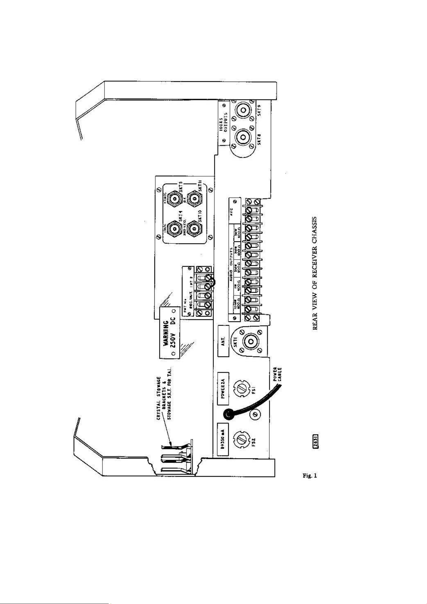
receiver (fig.1):-
[9]

Installation 10
1 Mc/s input/output: May be used diversity operation.
2nd V. F. O. output/input(3.6 – 4.6 Mc/s) For diversity operation and external chan-
nelizer crystal oscillator output.
1.7 Mc/s input/output For diversity operation and fine tuning unit
input.
R.F. (2 – 3 Mc/s) input: Input from an L.F. converter.
The above input/output connections are selected by internal linkage, the connections
should be made as follows:-
1 Mc/s input Remove “T” adaptor and place in clip pro-
vided on side of gusset plate. Connect the
free plugs PL12 to SKT3 and connect the
free plug PL2 to SKT2.
1 Mc/s output Disconnect plugs PL12 and PL2 and con-
nect “T” adaptor to socket SKT2. Connect
plugs PL12 and PL2 to the “T” adaptor.
2nd V.F.O. input Connect the free plug PL302 to SKT302.
2nd V.F.O. output Connect the free plug PL303A to SKT304.
1.7 Mc/s input Connect the free plug PL303A to SKT303.
1.7 Mc/s output Connect the free plug PL303A to SKT306.
(blue)
Note 1 When using the internal oscillators with crystals, the connections should be made
for outputs since the cable capacity will pull the internal crystal off frequency.
Note 2 The 1 Mc/s and 1.7 Mc/s crystal must be removed if an external source is applied
to the input socket. Stowage space is provided on the chassis for the crystals when
they are not in use.
AUTOMATIC VOLUME CONTROL.
8. The A.V.C. line is brought out to the terminal strip at the rear of the chassis for such
applications as diversity reception.

Installation 11

6. Operation
1. References to the controls are in capitals and are in accordance with the panel titles
adjacent to them (fig.2).
2. It should be noted that the method of operation of the receiver extremely simple,
depens largerly upon the purpose for which the receiver is being embloyed.
FUNCTION OF CONTROLS.
3. The front panel controls are described in the order in which they could be used for
setting-up prior to use.
POWER Makes and breaks the power supply to the mains transformer.
R.F. RANGE MC/S This control enables the selection of one any of five antenna ranges
plus two WIDEBAND positions, one of 75-ohms input impedance
and other a high impedance input of 2000-ohms.
R.F. ATTENUATOR This control enables the operator to reduce the level of all incoming
signals when strong unwanted signals are present which cannot be
rejected sufficiently by tuning the antenna.
MEGACYCLES This control selects the desired Mc/s frequency. The dial should be
checked periodically to ensure that its setting is reasonably central
with respect to the band in use. This is indicated by a reduction
of signal or noise on either side of the correct setting.
SYSTEM This switch provides facilities for STANDBY, MANUAL, A.V.C.,
CALIBRATION and CHECK B.F.O.
BANDWIDTH The two crystal filters determining the band- width are adjusted
to ensure that their centre frequencies are all within 50 c/s, thus
any bandwidth can be selected without retuning the receiver. Six
bandwidths are provided as follows:13 kc/s, 6.5 kc/s, 3 kc/s and 1.2 kc/s (L-C) 300 c/s and 100 c/s
(crystal)
A.F. GAIN The A.F. GAIN control adjusts the audio output.
KILOCYCLES This control selects the desired kc/s frequency. The calibration of
this scale may be checked at 100 kc/s intervals by setting the system
switch to the CAL. position and V.F.O. switch set to INT.
B.F.O. The B.F.O. ON/OFF switch makes or breaks H.T. to the beat
frequency oscillator.
B.F.O. NOTE KC/S The B.F.O. is exatly tuned to a central point on the I.F. ampli-
fier response when B.F.O. NOTE KC/S control is st to zero-beat
with the calibrator. Having standardized the B.F.O. frequency, the
frequency of an incoming signal may be accurately measured by setting the KILOCYCLES control to a zero-beat position; the B.F.O.
should de detuned in order to produce an acceptaple note for c.w.
reception.
[12]

Operation 13
R.F. TUNE If maximum sensitivity is not required, the antenna need not be
tuned unless strong unwanted signals are present. It should be
noted that the presence of very strong singnals anywhere within
the spectrum may cause crossmodulation unless the aerial is tuned.
Under these conditions, CARE MUST BE TAKEN TO AVOID
TUNING THE INPUT TO THE INTERFERING SIGNALS instead of the signal required. Familiarity with the tuning controls
will facilitate this.
R.F./I.F. GAIN The R.F./I.F. GAIN control is operative both in the MAN. and the
A.V.C. position of the SYSTEM switch. In the MAN.position of
the SYSTEM switch the setting of the control should be always at
a minimum consistent with satisfactory A.F. level. The following
should be noted when the SYSTEM switch is in the A.V.C. position. Reducing the I.F. gain results in a reduction of a A.V.C. loop
gain together with the a degraded A.V.C. characteristic. Therefore when in the A.V.C. position, it is desirable that the R.F./I.F.
GAIN control be set to maximum. A possible execption of this occurs when receiving interrupted signals in which the carrier is periodically switched off; in this case , receiver noise could be troublesome during the quiet intervals.
A.V.C. The choice of time-constant depends upon conditions. The LONG
time-constant (1 second) should be employed with the choice signals, the SHORT time-constant may be used with high speed telegraphy or voice. For hand (low) speed telegraphy, the MAN. position
of the SYSTEM switch should be used (refer to R.F./I.F. GAIN)
A.F. LEVEL The preset control sets the A.F. level in a separate A.F. stage for
feeding a 600-ohms, 10mW line. It is unaffected by the position of
the main A.F. GAIN control. IT IS MOST IMPORTANT that the
A.F. LEVEL is not turned towards its maximum position unless
the 10mW 600-ohms winding is suitable terminated.
LIMITER When swithced into use, the LIMITER reduces the effects of noise
peaks exceeding the level of a 30% modulated signal. It does not
introduce noticeable distortion below a 30% modulation level.
“S” METER With the METER switch in the R.F. LEVEL position the meter
indicates the signal diode current. In the A.F. LEVEL position, the
10mW, 600-ohms output only is monitored. A calibration mark is
provided at 10mW.
SPEAKER The loudspeaker may be switched ON or OFF as required. The two
telephone jack sockets remain in circuit in either position of the
SPEAKER switch. The insertion of a telephone jack disconnects
the loudspeaker.
V.F.O. This switch should be set to the EXT. position when a external 3.6
– 4.6 Mc/s source is applied.

Operation 14
PRELIMINARY SETTING-UP.
4. The instructions given below are concerned with tuning the receiver to a signal of
known frequency. These instructions (1) to (8) apply with the V.F.O. switch in either
position.
(1) Set the power switch to ON. Allow a few minutes for the receiver to warm-up.
(2) Set the R.F. RANGE MC/S switch to WIDEBAND.
(3) Set R.F. ATTENUATOR to MIN.
(4) Set A.F. GAIN control to its mid-position.
(5) Set SYSTEM switch to MAN.
(6) Set LIMITER and B.F.O. switch to OFF.
(7) Select bandwidth of 3 or 6.5 kc/s.
(8) Rotate the R.F./I.F. GAIN control to three-quarters of fully clockwise.
FILM SCALE CALIBRATION
5.
(1) Set the SYSTEM switch to CAL.
(2) Select BANDWIDTH of 3 kc/s.
(3) Set the KILOCYCLES scale to that of the 100 kc/s point which is nearest to
the frequency required and adjust the control accurately until a zero-beat note is
obtained. Move the milled cursor slide on the dial escutheon so that the pointer
coincides exactly with the selected 100 kc/s division.
(4) Restore all other controls to the preliminary setting shown in para.4. above.
B.F.O. CALIBRATION
6.
(1) Set the B.F.O. to on.
(2) Set the SYSTEM switch to CHECK B.F.O.
(3) Adjust the B.F.O. NOTE KC/S control to zero-beat.
(4) Restore all other controls to the preliminary setting shown in para.4. above.
TUNING
7.
(1) Set R.F. RANGE MC/S to the desired frequency band.
(2) Set R.F. ATTENUATOR to MIN.
(3) Set MEGACYCLES dial to the required integer (1 to 29). The position of maxi-
mum receiver noise will indicate the correct setting.
(4) Set SYSTEM switch to CAL.
(5) Set Bandwidth to 3 kc/s.
(6) Set A.F. GAIN to mid-position.
(7) Adjust KILOCYCLES scale to zero beat at the 100 kc/s point nearest to the
desired frequency.
(8) Adjust the milled cursor slide to coincide with this point.
(9) Switch B.F.O. on.
(10) Set SYSTEM switch to CHECK B.F.O.
(11) Adjust B.F.O. NOTE KC/S control to zero beat.

Operation 15
(13) Set KILOCYCLES scale to the required frequency and critically tune for zero
beat in order to centralize the signal within the I.F. pass-band.
(14) Adjust R.F. TUNE for maximum signal (or noise). For optimum c.w. reception,
“off-tune” the B.F.O. to produce an acceptaple beat note.
(15) Set the A.F. GAIN to its maximum clockwise position and adjust the output level
with the R.F./I.F. GAIN control.
(16) For m.c.w. or voice reception, switch B.F.O. off.
(17) Set the SYSTEM switch to A.V.C. if required.
(18) Set BANDWIDTH for optimum reception.
“S” METER
8. The “S” meter should be correctly set to zero.
9. With no antenna connected, set the R.F. ATTENUATOR to MAX. Set the SYSTEM
switch to A.V.C. Turn the R.F./I.F. GAIN control to the maximum clockwise position.
NOTE: Unless the R.F./I.F. GAIN control is in the maximum position, the ”S” meter
calibration is upset.
10. Remove the plated cap below the meter. Adjust the setting of the balance control
(accessible through the hole in the panel) by means of a screwdriwer until the meter
reads zero.

Operation 16

7. Brief Technical Description
1. This section describes briefly, with the aid of the block diagram fig. 3, the basic theory
of operation. For a more detailed explanation of the receiver, DETAILED CIRCUIT
DESCRIPTION, should be consulted.
SIGNAL INPUT
2. The receiver is designed for an input impedance of 75-ohms for all positions of the
R.F. RANGE switch except WIDEBAND; in the WIDEBAND position the input
impedance is 2000-ohms.
FIRST MIXER
3. Input signals between 0.98 and 30 Mc/s are via an R.F. amplifier and a 30 Mc/s
low-pass filter to the first mixer (M1) where they are mixed with the output from a
variable frequency oscillator VFO-1 (MEGACYCLES tuning). This oscillator has a
frequency range of 41.5 to 69.5 Mc/s. The first I.F. stage is in effect a band-pass filter
tuned to 40 Mc/s ±650 kc/s. Thus, according to the setting of VFO-1, any spectrum
of signals 1 Mc/s wide and existing in the range 0.98 to 30 Mc/s can be mixed in M1
to produce an output acceptable to the first I.F. band-pass filter.
4. It should be noted at this stage that the exact setting of VFO-1 is determined by
conditions in the second mixer and harmonic mixer circuit ; These restrict the possible
settings to position 1 Mc/s apart (e.g. 41.5, 42.5, 43.5 Mc/s, etc.).
HARMONIC GENERATOR AND MIXER
5. The output from a 1 Mc/s crystal oscillator is connected to a harmonic generator.
The harmonics derived from this stage are passed through a 32 Mc/s low-pass filter
and mixed with the output from VFO-1 in the harmonic mixer. This mixer provides
an output at 37.5 Mc/s which is amplified before passing through a band-pass filter
tuned to 37.5 Mc/s with a bandwidth of ±150 kc/s.
6. The presence of this filter restricts the setting of VFO-1 to an exact number of Mc/s
plus 37.5 Mc/s in order to give an output acceptaple to the filter and amplifier. As a
result, the first V.F.O. must be tuned in 1 Mc/s steps.
SECOND MIXER
7. The 40 Mc/s first I.F. signal is mixed in the second mixer (M2) with the 37.5 Mc/s
output from the harmonic mixer in order to produce an output consisting of a 1 Mc/s
spectrum in the frequency range 2 – 3 Mc/s (second I.F.).
8. To clarity this method of operation, some examples of dial settings and intermediate
frequencies corresponding to various incoming signals are tabulated below:
Dial Settings Signal Freq. VFO-1 Xtal harmonic 1st I.F. 2nd I.F.
Mc/s kc/s (fs) Mc/s (fo)Mc/s (nfc)Mc/s Mc/s Mc/s
4 1.000 5.0 44.5 7th 39.5 2.0
5 0 5.0 45.5 8th 40.5 3.0
18 600 18.6 58.5 21st 39.9 2.4
[17]

Brief Technical Description 18
9. Frequency drift of VFO-1 within the limits of the 37.5 Mc/s filter bandwidth, does
not affect the frequency stability of the receiver. A change in this oscillator frequency
will alter the first I.F. to the same extent and in the same sense as the nominal
37.5 Mc/s signal from the harmonic mixer. Therefore the difference frequency from
M2 will remain constant.
THIRD MIXER
10. The 2 – 3 Mc/s receiver, which follows M2, is preceded by a pre-tuned bandpass filter.
The 2 – 3 Mc/s output from the filter is mixed in the third mixer with either the output
from the second variable frequency oscillator VFO-2 or an external signal within the
frequency range of 3.6 to 4.6 Mc/s to provide the third intermediate frequency of 1.6
Mc/s.
FOURTH MIXER
11. The 1.6 Mc/s intermediate frequency is mixed in the fourth mixer (M4) with the
1.7 Mc/s output from the 1.7 Mc/s oscillator/amplifier to provide the fourth and final
intermediate frequency of 100 kc/s.
FOURTH I.F. STAGE
12. The final I.F. stages are preceded by crystal lattice and L-C filters which provide six
alternative bandwidths. Separate signal and A.V.C. diodes are employed and alternative switched time-constants give the optimum conditions for telegraphy and telephony
reception. An additional I.F. amplifier is incorporated to give an independent output
at 100 kc/s.
A.F. STAGES
13. Two independent audio frequency stages are incorporated for either line output or
headphone sockets and internal loudspeaker; each stage is provided with a level control
(see TECHNICAL SPECIFICATION).
CRYSTAL CALIBRATOR
14. A crystal calibrator unit is incorporated to enable the scale of VFO-2 to be checked at
100 kc/s intervals when the V.F.O. switch is set to INT. position. These check points
are obtained from a regenerative divider controlled by the 1 Mc/s crystal oscillator.

8. Detailed Circuit Description
1. Reference should be made to the circuit diagram at the end of this handbook.
AERIAL CIRCUIT
2. A 75-ohms unbalanced aerial source is connected to the tuned R.F. amplifier through
a three-section 30 Mc/s low-pass filter and a five- position attenuator covering a range
of 0 to 40 dB. Switch S2 selects wide- band 75-ohms or wideband (high impedance) or
any one the five double-tuned aerial coils L4-L8 for tuned operation. These aerial coils
are aligned by means of dust iron cores. The aerial is tuned by a capacitor C18A/B
which is switched out of circuit in both wideband positions.
R.F. AMPLIFIER
3. The incoming signal is fed via C28 and grid stopper R25 to the grid of V3B; the
R.F. stage (V3) employs a variable-mu, low-noise double- triode; the two halves of the
valve are connected in cascode so as to utilize the low-noise high-gain properties of
the valve. A delayed A.V.C. voltage, derived from a shunt diode network, is applied to
the grid of V3B when the signal level is approximately 10µV. The capacitors C40 and
C41 ensure that the cathode is adequately decoupled over the wide frequency range.
Ferrite beads have been fitted to the heater lead, connected to pin 4, the anode of V3A
and the cathode of V3B adjacent to C41, to prevent parasitic oscillations occurring.
30 MC/S LOW-PASS FILTER
4. The amplified signal is passed to a 30 Mc/s low-pass filter which has a substantially
flat responseover the frequency range. L27, C47 and R28 constitute the first ‘L half
Section’ of the filter. The signal is then fed at low impedance (680-ohms) through the
coupling capacitor C74 and the grid stopper R45 to the control grid of V7, the first
mixer stage. The input capacitance of V7 forms the capacitance to chassis betweeenL15
and L17 required to the filter network.
NOTE:This capacitance is not critical, therefore no adjustment will be necessary should
V7 be changed.
FIRST VARIABLE FREQUENCY OSCILLATOR (VFO-1)
5. This circuit comprises a cathode-coupled Hartley oscillator stage (V5) which may be
continously tuned over the frequency range of 40.5 to 69.5 Mc/s. The frequency determining components are an inductance L36 and a variable capacitance C76. Alignment
is accomplished by adjusting aluminium core of L36 and the trimming capacitor C77.
The variable capacitor C76 is coupled to the Mc/s dial which is calibrated from 0 to
29 Mc/s. The anode load consists of L20, a compensating inductance which is wound
on a 470-ohm resistor R18. The oscillator is coupled via C85 to the signal grid of the
first mixer stage V7 and also via C42 to the control grid of the harmonic mixer V4.
NOTE:The Mc/s dial calibration may be affected if V5 if changed. The necessary correc-
tion may be made by adjusting C77 with the Mc/s dial set to 29 Mc/s.
[19]

Detailed Circuit Description 20
FIRST MIXER (M1)
6. The outputs from the 30 Mc/s low-pass filter and the variable frequency oscillator
VFO-1 are fed to the signal grid of the mixer stage (V7) which produces a signal at
40 Mc/s. The signal is then passed to a 40 Mc/s band-pass filter which forms the
anode load of this stage.
40 MC/S BAND-PASS FILTER
7. The 40 Mc/s band-pass filter consists of eight over-coupled tuned circuits connected
in cascade and is tuned by the trimming capacitors C21, C33, C43, C53, C61, C70,
C79 and C88. This filter, which has a passband of 40 Mc/s ±650 kc/s, ensures that
only the required 1 Mc/s spectrum of signals is passed to the second stage. This filter
is deliberately set to a slightly wider passband than is theoretically required, to allow
for possible drift in VFO-1.
1 MC/S CRYSTAL OSCILLATOR/AMPLIFIER
8. The frequency of the crystal oscillator V1 may be set precisely to 1 Mc/s by adjusting
the trimming capacitor C2A. The crystal XL1 which is connected between the control
grid and the screen grid is electron coupled to the anode. The anode coil L2 is adjusted
to resonate at 1 Mc/s by means of a dust iron core. The fixed capacitors C9, C10 and
C11 complete the tuned circuit. When an external signal is applied to socket SK3, the
valve operates as an amplifier.
9. The output from V1 is capacitance-coupled to the harmonic generator V2 and via
SK2 to a “T” adptor for feeding a 1 Mc/s input into the L.F. converter and also the
control grid of the mixer valve V13.
HARMONIC GENERATOR
10. The 1 Mc/s signal is fed via coupling capacitor C8 to the control grid of the harmonic
generator V2. The H.T. is fed to the screen grid via R12 and is decoupled by C8A.
Harmonics produced at this stage are passed to a 32 Mc/s low-pass filter.
32 MC/S LOW-PASS FILTER
11. The megacycle harmonics are fed through a 32 Mc/s low-pass filter circuit to prevent
harmonics other than those required from passing to the harmonic mixer (V4). Limited
control over the cut-off frequency is provided by C7 which is adjusted to equalize the
output from yhe filter at the frequencies corresponding to 28 and 29 Mc/s on the
MEGACYCLE dial.
HARMONIC MIXER
12. The outputs from the 32 Mc/s low-pass filter and VFO-1 are mixed in the harmonic
mixer by applying the filtered megacycle harmonics to the suppressor grid and the
output from the VFO-1 to the control grid. The 37.5 Mc/s output is selected by the
tuned anode load, consisting of a fixed capacitor C50 and an inductance L28 which
may be adjusted by means of a dust iron core, and coupled by C51 to V6. R36 is grid
stopper.
2-STAGE 37.5 MC/S AMPLIFIER (1)
13. The anode load of V6 is a tuned circuit consisting of a fixed capacitor C67 and an
inductor L33 Which is tuned to 37.5 Mc/s. Frequency adjustment is by the dust iron

Detailed Circuit Description 21
core L33. This stage feeds the amplified signal via C68 to the following stage V8. The
37.5 Mc/s signal is then passed to the 37.5 Mc/s band-pass filter. The anode load of
this stage is provided by this filter.
37.5 MC/S BAND-PASS FILTER
14. The 37.5 Mc/s band-pass filter consists of eight under-coupled tuned circuits arranged
in cascade. These filter sections may be tuned by C24, C35, C45, C55, C63, C72, C81
and C91 respectively. This filter, which has a passband of 300 kc/s, allows for possible
drift in VFO-1. The narrow passband and high rejection to frequencies outside the
passband prevent spurious signals from reaching the second mixer stage (V9).
37.5 MC/S AMPLIFIER (2)
15. The filtered 37.5 Mc/s signal is further amplified by V10 before being passed to the
second mixer stage (V9). To prevent interaction between the 40 Mc/s band-pass filter
and the 37.5 Mc/s tuned circuit (L50 and C113) and to enable either circuit to be
adjusted without affecting the other, a balancing circuit is included which is shown in
simplified form in fig. 4. The 40 Mc/s signal is introduced into the 37.5 Mc/s tuned
circuit at a point of zero R.F. potential since L50 is centre tapped and C108 is adjusted
to be equal to the total of the capacitance of V10 anode to chassis. C107 and the input
capacitor of V9.
NOTE:The anode load of V10 is adjusted to 37.5 Mc/s by adjusting the dust iron core
in L50. The balancing circuit will be affected if V9 or V10 is changed.
SECOND MIXER (M2)
16. This mixer (V9) produces the second intermediate frequency of 2 – 3 Mc/s by mixing
the 40 Mc/s I.F. and the 37.5 Mc/s signal. The tuned circuit formed by L300, C300
remove the 37.5 Mc/s frequency whilst the other tuned circuit formed by L301, C301
remove the 6 Mc/s frequency so that only the second I.F. is passed to the 2 – 3 Mc/s
band-pass filter preceding the third mixer.
2 – 3 MC/S PRE-TUNED BAND-PASS FILTER
17. This filter consists of two pre-tuned band pass filter sections. The characteristic
impedance of the filter is 1000 ohms.

Detailed Circuit Description 22
THIRD MIXER
18. The output from the 2 – 3 Mc/s band-pass filter is resistance-capacitance coupled
to the signal grid of V25 together with the output (3.6 – 4.6 Mc/s) from the second
V.F.O. amplifier V11 when the V.F.O. switch (S300) is set to the INT. position. With
the V.F.O. switch set to the EXT. position, V11 operates as a buffer amplifier. This
mixer (V25) produces the third intermediate frequency of 1.6 Mc/s. The signal is then
fed to a 1.6 Mc/s band-pass filter which forms the anode load of this stage.
19. The 1.6 Mc/s band-pass filter consists of two double-tuned I.F. trans- formers, the
first section of the filter is formed by C320, L306, L309 and C325 and the second
section by C332, L313, L314, C334. This filter has a bandwidth of 13 kc/s.
SECOND VARIABLE FREQUENCY OSCILLATOR (VFO-2)
20. The second variable frequency oscillator, covering a frequency range 3.6 to 4.6 Mc/s,
is an electron coupled Hartley circuit embloying one half of double-triode V12. The
oscillator frequency is determined by an inductance L55, two fixed capacitors C303,
C305, a trimming capacitor C306 and a variable capcitor C301. The KILOCYCLES
scale which is calibrated between 0 and 1000 kc/s is coupled to this variable capacitor.
21. The output from VFO-2 is resistance-capacitance coupled to the grid of V12A, a
cathode-follower stage. With the V.F.O. switch set to the INT. position the output
from V12A is fed via PL305 and PL300A to the control grid of the second v.f.o.
amplifier V11. In the EXT. position the external 3.6 to 4.6 Mc/s signal is fed to V11.
FOURTH MIXER
22. The output from the 1.6 Mc/s band-pass filter is directly coupled to the signal grid
of a pentagrid valve V26; it is mixed with a 1.7 Mc/s signal from V27 fed via the
coupling capacitor C339 to the oscillator grid of V26. The resistor R68 completes the
d.c. path from this grid to earth. The 100 kc/s output from this mixer stage is then
fed via SK6, PL6 to the crystal filter unit.
1.7 MC/S CRYSTAL OSCILLATOR/AMPLIFIER
23. The frequency from the crystal oscillator C27 may be set precisely to 1.7 Mc/s by
adjusting the trimming capacitor C337. The crystal XL300 which is connected between
the control grid and the screen grid is electron coupled to the anode. When an external
signal is applied to socket SK303A the valve operates as an amplifier. The output from
this circuit is fed via C339 to the oscillator grid of the fourth mixer V26.
CRYSTAL FILTER
24. Six alternative switched I.F. bandwidths are available as follows:-
100 c/s
300 c/s
1.2 kc/s
3.0 kc/s
6.5 kc/s
13.0 kc/s
Crystal
L − C

Detailed Circuit Description 23
25. In the crystal positions the fourth mixer anode is connected to L48 in the crystal filter.
L47 and L49 provide a balanced output which is tuned by capacitors C109 and C110.
In the 100 c/s position, the balanced output is connected via crystals XL2 and XL5
to the first tuned section of the 100 c/s L-C filter. The differential trimmer C118 is
the phasing control for this bandwidth. XL3, XL6 the capacitor C119 form a similar
circuit for the 300 c/s position. Damping resistors R64 and R65 are connected across
the tuned circuits to obtain the required bandwidth.
100 KC/S L-C FILTER
26. This filter consists of four tuned circuits arranged in cascade. In the L-C bandwidth
positions, the signal is fed to the tuned circuit formed by L61 and the combination
of the capacitors C145, C146, C146A and C147. The second section consists of L62
and L63 in series with C152, C152A and C153. The final section consisting of L68
and L71 in series with C161 and C162, is damped by the series resistors R86, R87A
and R88 according to the bandwidth. In the L-C positions the output is taken from
a capacitive divider formed by C161 and C161A with C170, to equalize the gains in
the L-C and crystal bandwidth positions.
27. The L-C banwidths are obtained by varying the degree of coupling between each
section of the filter in addition to the damping resistors in the final stage. The capacitor
C175 is included to compensate for the effective reduction of the input capacitance of
V14, appearing across the tuned circuit, when switching from crystal to L-C positions.
28. To maintain the input capacitance of the L-C filter, in the crystal positions, a trimming
capacitor C148 is switched into circuits. This trimmer is adjusted to be equal to the
output capacitance of V26 and the screened cable. In the crystal bandwidth positions,
the L-C filter is operating in its narrow bandwidth positions, i.e. 1.2 kc/s.
NOTE:The 470-kilohm damping resistors R77 and R80 are disconnected except during
filter alignment.
FIRST 100 KC/S I.F. AMPLIFIER
29. The output from the L-C filter is passed through a coupling capacitor C164 to the
control grid of the pentode amplifier valve V14. This grid is returned via R96 to the
A.V.C. line which is filtered at this point by R102 and C173. The screen potential is
derived from a potential divider formed by R93, R97 and RV4. This stage is coupled
to the second I.F. amplifier and the I.F. output stage by a double tuned transformer
having an over-coupled characteristic.
SECOND 100 KC/S I.F. AMPLIFIER
30. The signal from the first I.F. tranformer is fed through the grid stopper R114 to the
control grid of the second I.F. amplifier. H.T. is supplied to the screen via the dropping
resistor R113 and is decoupled by C181. The anode load is tuned circuit consisting of
L77, C192 and C191. This circuit is heavily damped by R112. The secondary winding
L78 and L79 is tuned by C195 and C195B with R120A as a damping resistor. The
output is fed to the diode detector anode.
DIODE DETECTOR
31. The low potential end of L79 is connected through the R.F. filter (C209, R128, C210,
C219 and C211) to the diode load R130. With the meter switched to R.F. LEVEL, the

Detailed Circuit Description 24
meter indicates the detector diode current. The resistor R131 is incluced to complete
the diode detector circuit when the meter is switched out of circuit.
NOISE LIMITER
32. The noise limiter diode (pins 2 and 5 of V21) is connected in a series circuit to operate
at approximately 30% modulation. its operation is explained with reference to fig.5.
33. The d.c. path from point A is through R134, R135, the diode and R137. The A.F. signal
path from detector diode load is through C216, the diode and C218 when S8 is open.
In the presence of a signal, a negative potential varying with the depth of modulation,
will be developed at point A thus causing the diode to conduct. The negative potential
at B, will be lower than at A and will be maintained at a constant level due to the
long time constant of R134 and C217. R135 allows the cathode potential to vary in
sympathy with the modulation provided the modulation depth does not exceed 30%.
The potential appearing at the cathode of the noise limiter diode therefore consists of
a steady negative potential with the modulation superimposed. When noise impulses
corresponding to high modulation peaks appear at point A and via C216 at point C,
the voltage across the diode changes sign thereby causing the diode to stop conducting
and open-circuit the A.F. signal path. With S8 in the OFF position the limiter is
inoperative.
A.V.C. AND T.C. DIODE
34. The signal appearing at the anode of V16 is passed through the capacitor C139 to the
anode of the A.V.C. diode. The diode load is formed by R116. A positive potential
derived from R120, R121 and R122, supplies the required A.V.C. delay voltage to the
cathode of this diode.When A.V.C. switch is in the SHORT position and the SYSTEM
switch set to a position in which the A.V.C. is operative, i.e. A.V.C., CAL. or CHECK
B.F.O., the anode of the A.V.C. diode is connected to the A.V.C. line via L81 and
R127. The choke L81 is tuned by C203 to a frequency slightly below 100 kc/s so that
is presents a small capacitance at 100 kc/s, thus R127 is prevented from shunting
the diode load. When the signal level falls, the capacitors C182 and C173 discharge
through R118, R127 and L81 into the diode load resistor R116. The A.V.C. potential
is brought out via R123 to the tag strip at the rear of the receiver for external use if

Detailed Circuit Description 25
required. With the SYSTEM switch set to the MANUAL position, the A.V.C. line is
connected to the R.F./I.F. GAIN control RV1, thus the gain of the 100 kc/s amplifiers
may be varied by adjusting the negative potential applied to the A.V.C. line.
AUDIO OUTPUT
35. Audio frequencies are applied to the control grid of V23B via RV2 the A.F. GAIN
control. The output transformer (T2) provides four separate outputs as follows: 1W
into 3-ohms, and three windings supplying 3mW into 600- ohms.
36. The internal loudspeaker (which may be switched out of circuit by operating S11) is
connected across the 3-ohm winding. The headphone jacks JK1 and JK2 are connected
across one of the 600-ohms windings.
A.F. LINE OUTPUT
37. The audio frequencies are also applied to the grid of V23A via RV3, the A.F. GAIN
LEVEL control; this control presets the level from output transformer T3. The transformer provides a 10mW output at 600-ohms which is suitable for direct connection to
landlines. A bridge rectifier MR1 is connected across the output via R142 and R143.
Th meter may be switched across the rectifier circuit so that the operator can monitor
the A.F. output.
BEAT FREQUENCY OSCILLATOR
38. The beat frequency oscillator (V19) employs an electron-coupled Harley circuit. The
oscillation frequency is determined by a fixed inductor L82 and a variable capacitor
C200 in parallel with C202 and C201. the trimming capacitor C201 is adjusted to
produce an output frequency of preisely 100 kc/s when the beat frequency oscillator
frequency control is set to zero. Bias is applied to this valve by C199 and R125.
39. The B.F.O. output is coupled to the diode detector anode via C215. The B.F.O. is
supplied with H.T. via S7 except when SYSTEM switch is in the CAL. or STANDBY
positions.
100 KC/S I.F. OUTPUT
40. The control grid of V17 is connected to the secondary of the first 100 kc/s I.F. transformer which feeds the stage with the 100 kc/s signal. The screen resistor R108 and
the cathode bias resistor R115 are of the same values as used in the scond 100 kc/s
I.F. amplifier, hence the A.V.C. characteristic of this stage is identical to that of the
main receiver. The anode load resistor R109 feeds the auto transformer L76 via blocking capacitor C189. This transformer provides a 70-ohms output at PL8 and PL9 for
external applications.
NOTE:PL8 and PL9 are connected in parallel, therefore only one 100 kc/s output is
available at 75-ohms, and to avoid a mismatch the other connection should be
made at high impedance.
CRYSTAL CALIBRATION
41. The crystal calibrator, controlled by the 1 Mc/s crystal or by the 1 Mc/s standard
input to V1, feeds signals at 100 kc/s intervals to the signal grid of the third mixer
stage to provide calibration check points. The calibration can only be carried out when
the V.F.O. switch S300 is set to the INT. position.

Detailed Circuit Description 26
42. The 1 Mc/s signal, fed through SK2, is connected through PL2 and the grid stopper
R83 to the first grid of the mixer valve V13. The anode load consists of a 100 kc/s tuned
circuit (L70, C167) and is coupled to the control grid of V15 through the capacitor
C168. The anode load of V15 (L75, C117) is tuned to 900 kc/s and is coupledvia C178
to the third grid of V13. V15 is heavily biased so that it functions as a frequency
multiplier.
43. An output of 900 kc/s, appearing across the tuned circuit (L75, C177) is coupled
to grid 3 of V13 thereby producing a difference frequency of 100 kc/s relative to the
1 Mc/s input. The 100 kc/s output appears across the anode tuned circuit (L70, C167)
and is fed to the control grid of V15. The ninth harmonic is selected in turn by the
anode tuned circuit (L75, C177) of V15 and fed back to the third grid of V13 to
provide the beat frequency of 100 kc/s with the 1 Mc/s input. This crystal controlled
regenerative circuit is thus self-maintaining. The 100 kc/s output is obtained from the
coil L69 which is mutually coupled to L70 and fed via the octal plug (PL7) to the
cathode-follower V12A.
POWER SUPPLIES
44. The primary of the mains transformer is tapped to provide for inputs of 100 – 125
and 200 – 250V. To remove mains-borne interference the capacitors C224 and C225
are incluced. The secondary winding of T1 feeds a bridge-connected full-wave rectifier
MR4, MR5, MR6 and MR7 whose output is filtered by C206, L80 and C198 and fed
via the receiver muting relay RL1/1 to the SYSTEM switch S5. A 120-ohm resistor
R124 is connected between the negative line and earths thus providing a negative 25V
d.c. supply for gain control purposes.
SYSTEM SWITCH
45. The following conditions exist for each setting of the SYSTEM switch. The link on
H.T. adaptor terminal is assumed to be in position.
(1) STANDBY S5A disconnects the H.T. from all stages and connects R119A
across the H.T. as a compensating load.
(2) MANUAL (a) The H.T. passes through S5A, S5B and S5C to all stages ex-
cept the calibration unit.
(b) S5F connects H.T. to the B.F.O. when S7 is switched on.
(c) The A.V.C. line is disconnected from the A.V.C. diode by S5D
and connected to the R.F./I.F. GAIN control (RV1) by S5E.
(3) (a) (2)(a) and (2)(b) are applicable.
(b) S5D connects the A.V.C. line to the A.V.C. diode.
 Loading...