

Page 1

WARRANTY INFORMATION
Quatech Inc. warrants the ES-2000/ES-3000
free of defects for one
purchase. Quatech Inc. will repair or replace any board
that fails to perform under normal operating conditions and
in accordance with the procedures outlined in this document
during the warranty period. Any damage that results from
improper installation, operation, or general misuse voids
all warranty rights.
Although every attempt has been made to guarantee the
accuracy of this manual, Quatech Inc. assumes no liability
for damages resulting from errors in this document. Quatech
Inc. reserves the right to edit or append to this document
at any time without notice.
Please complete the following information and retain
for your records. Have this information available when
requesting warranty service.
DATE OF PURCHASE:
MODEL NUMBER: ES-2000/ES-3000
PRODUCT DESCRIPTION: EIGHT
(1) year from the date of
CHANNEL RS-422/RS-485
to be
ASYNC.
SERIAL NUMBER:
IBM PC/XT/ATTM, PS/2TM, and Micro ChannelTM are
trademarks of International Business Machines.
COMMUNICATIONS ADAPTER
i
Page 2

TABLE OF CONTENTS
WARRANTY INFORMATION . . . . . . . . . . . . i
LIST OF FIGURES . . . . . . . . . . . . . iii
I. INTRODUCTION . . . . . . . . . . . . . . . . 1
II. BOARD DESCRIPTION . . . . . . . . . . . . . 1
III. 16552 FUNCTIONAL DESCRIPTION . . . . . . . . 3
INTERRUPT ENABLE REGISTER . . . . . . . . 4
INTERRUPT IDENTIFICATION REGISTER . . . . 5
FIFO CONTROL REGISTER . . . . . . . . . . 7
LINE CONTROL REGISTER . . . . . . . . . . 8
MODEM CONTROL REGISTER . . . . . . . . . 10
LINE STATUS REGISTER . . . . . . . . . . 11
MODEM STATUS REGISTER . . . . . . . . . . 13
ALTERNATE FUNCTION REGISTER . . . . . . . 14
SCRATCHPAD REGISTER . . . . . . . . . . . 14
IV. FIFO MODE OPERATION . . . . . . . . . . . . 15
FIFO INTERRUPT OPERATION . . . . . . . . 15
FIFO POLLED OPERATION . . . . . . . . . . 15
V. BAUD RATE SELECTION . . . . . . . . . . . . 16
VI. ADDRESSING . . . . . . . . . . . . . . . . . 18
VII. INTERRUPTS . . . . . . . . . . . . . . . . . 18
INTERRUPT STATUS REGISTER . . . . . . . . 19
VIII. PROGRAMMABLE OPTION SELECT . . . . . . . . . 20
IX. OUTPUT CONFIGURATIONS . . . . . . . . . . . 22
AUXILIARY CHANNEL CONFIGURATION . . . . . 22
HALF DUPLEX OPERATION . . . . . . . . . . 23
X. EXTERNAL CONNECTIONS . . . . . . . . . . . . 25
XI. HARDWARE INSTALLATION . . . . . . . . . . . 26
XII. ADDITIONAL ADDRESSING . . . . . . . . . . . 27
XIII. SPECIFICATIONS . . . . . . . . . . . . . . . 32
i
Page 3

LIST OF FIGURES
Figure 1. ES-2000/ES-3000 board layout . . . . . 2
Figure 2. 16552 register map . . . . . . . . . . 3
Figure 3. Interrupt identification register . . 6
Figure 4. FIFO receiver trigger levels . . . . . 7
Figure 5. Parity options . . . . . . . . . . . . 9
Figure 6. Word length and stop bit options . . . 9
Figure 7. Multi-function output pin control . . 14
Figure 8. Input clock frequency options . . . . 16
Figure 9. Baud rate selections . . . . . . . . . 17
Figure 10. Baud rate selections . . . . . . . . . 17
Figure 11. ES-2000/ES-3000 address assignments . 18
Figure 12. Interrupt selections . . . . . . . . . 20
Figure 13. ES-2000/ES-3000 POS implementation . . 21
Figure 14. Auxiliary channel control jumpers . . 22
Figure 15. Half duplex operation control jumper . 23
Figure 16. Output control block diagram . . . . . 24
Figure 17. Output control block diagram . . . . . 24
Figure 18. Output connector . . . . . . . . . . . 25
Figure 19. Output connector signal definitions . 25
Figure 20. QTINSTAL.EXE opening menu . . . . . . 28
Figure 21. QTINSTAL.EXE address selection menu . 29
Figure 22. QTINSTAL.EXE address input . . . . . . 30
Figure 23. QTINSTAL.EXE updated address menu . . 31
iii
Page 4

INTRODUCTION
I. INTRODUCTION
The Quatech ES-2000 provides eight independent
asynchronous RS-422 serial communication channels for
systems utilizing the MicroChannel architecture. The ES3000 is an RS-485 version of the adapter. The eight ports
of the ES-2000/ES-3000 occupy a contiguous 64 byte block of
I/O address space. The base address of this block may be
located anywhere within the available I/O address range of
the system.
The ES-2000/ES-3000 serial interfaces are realized
through four 16552 DUARTs (Dual Universal Asynchronous
Receiver / Transmitters). The 16552 is a two channel
version of the 16550 used in the IBM PS/2 family of personal
computers and is compatible with the 8250 and 16450 UARTs
used in the PC/XT/AT models. In addition, the 16550 and
16552 support transmit and receive FIFOs to reduce CPU
overhead at higher data rates.
Address and interrupt selections are accessed through
the Programmable Option Select using the IBM installation
utilities. In addition, jumpers are provided to select
input clock frequency and to control the information
exchanged on the auxiliary channels.
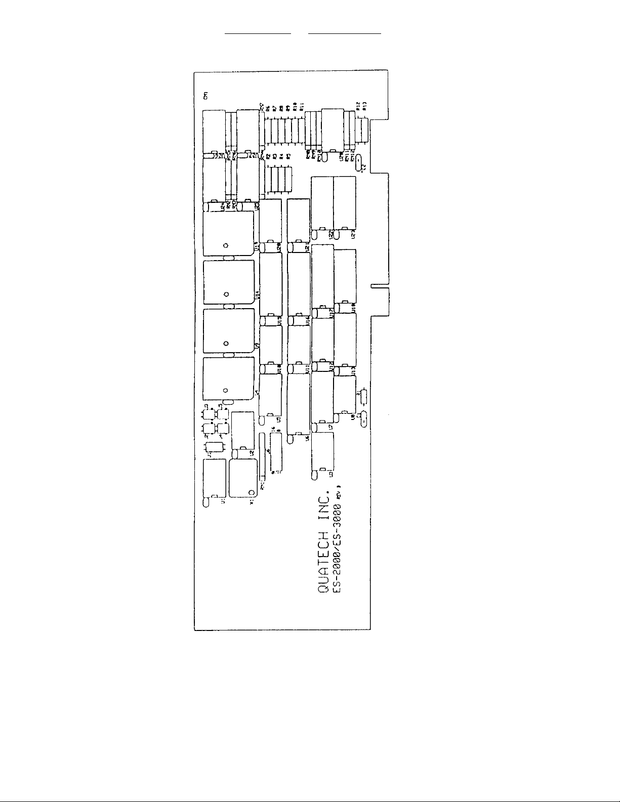
II. BOARD
DESCRIPTION
A component diagram of the ES-2000/ES-3000 showing the
locations of the 16552 DUARTs, clock frequency jumper,
auxiliary channel control jumpers, and D-62 output connector
is shown in figure 1. Channels 1 and 2 are contained in the
DUART labeled U4, channels 3 and 4 in U9, 5 and 6 in U14,
and 7 and 8 in U19. Channels 1 - 4 of the ES-2000/ES-3000
also have an auxiliary channel available for exchange of the
RTS-CTS handshake pair. The auxiliary channels are
controlled by jumpers J2 - J5 respectively. The input clock
frequency for all channels is selected using jumper J1. All
channels are output via the high density D-62 connector CN1.
On the ES-2000, the driver circuit consists of four RS422 drivers (U20, U21, U24, and U26), three RS-422 receivers
(U25, U27, and U28) and twelve 100_ termination resistors
(R2 - R13). On the ES-3000, these are replaced by RS-485
drivers and receivers and 120_ termination resistors.
iii
Page 5
FUNCTIONAL DESCRIPTION
Figure 1. ES-2000/ES-3000 board layout.
iii
Page 6

FUNCTIONAL DESCRIPTION
III. 16552 FUNCTIONAL DESCRIPTION
The 16552 is two channel version of the 16550 Universal
Asynchronous Recevier / Transmitter (UART). The two
channels are completely independent except for the common
clock oscillator input. Each channel of the 16552 enters
character mode after reset and in this mode appears as a
16450 to application software. An additional FIFO mode can
be selected to reduce CPU overhead at high data rates. The
FIFO mode increases performance by providing two internal
16-byte FIFOs (one transmit and one receive) to buffer data
and reduce the number of interrupts issued to the CPU.
Other features include:
Programmable baud rate, character length,
parity, and number of stop bits
Automatic addition and removal of start, stop,
and parity bits
Independent and prioritized transmit, receive
and status interrupts
Transmitter clock output to drive receiver
logic
The following pages provide a brief summary of the
internal registers available for each channel of the 16552
DUART. The registers are addressed as shown in figure 2
below.
+---------------+----------------------------------------+
| DLAB A2 A1 A0 | REGISTER DESCRIPTION |
+---------------+----------------------------------------+
| 0 0 0 0 | Receive buffer (read only) |
| | Transmit holding register (write only) |
| 0 0 0 1 | Interrupt enable |
| 0 0 1 0 | Interrupt identification (read only) |
| | FIFO control (write only) |
| x 0 1 1 | Line control |
| x 1 0 0 | MODEM control |
| x 1 0 1 | Line status |
| x 1 1 0 | MODEM status |
| x 1 1 1 | Scratch |
| 1 0 0 0 | Divisor latch (least significant byte) |
| 1 0 0 1 | Divisor latch (most significant byte) |
| 1 0 1 0 | Alternate function |
+---------------+----------------------------------------+
Figure 2. Register map for one channel of the 16552
DUART. DLAB is accessed through the Line
Control Register.
iii
Page 7

FUNCTIONAL DESCRIPTION
INTERRUPT
ENABLE REGISTER
+-------+
D7 | 0 |
+-------+
D6 | 0 |
+-------+
D5 | 0 |
+-------+
D4 | 0 |
+-------+
D3 | EDSSI |----- MODEM status
+-------+
D2 | ELSI |----- Receiver line status
+-------+
D1 | ETBEI |----- Transmitter holding register empty
+-------+
D0 | ERBFI |----- Received data available
+-------+
EDSSI - MODEM Status Interrupt:
When set (logic 1), enables interrupt on clear to
send, data set ready, ring indicator, and data
carrier detect.
ELSI - Receiver Line Status Interrupt:
When set (logic 1), enables interrupt on overrun,
parity, and framing errors, and break indication.
ETBEI - Transmitter Holding Register Empty Interrupt:
When set (logic 1), enables interrupt on transmitter
register empty.
ERBFI - Received Data Available Interrupt:
When set (logic 1), enables interrupt on received
data available or FIFO trigger level.
iii
Page 8

FUNCTIONAL DESCRIPTION
INTERRUPT
+------+
D7 | FFE |--+
+------+ +-- FIFO enable
D6 | FFE |--+
+------+
D5 | 0 |
+------+
D4 | 0 |
+------+
D3 | IID2 |--+
+------+ |
D2 | IID1 | +-- Interrupt identification
+------+ |
D1 | IID0 |--+
+------+
D0 | IP |----- Interrupt pending
+------+
FFE - FIFO Enable:
IIDx - Interrupt Identification:
IDENTIFICATION REGISTER
When logic 1, indicates FIFO mode enabled.
Indicates highest priority interrupt pending if any.
See IP and figure 3. NOTE: IID2 is always a logic 0
in character mode.
IP - Interrupt Pending:
When logic 0, indicates that an interrupt is pending
and the contents of the interrupt identification
register may be used to determine the interrupt
source. See IIDx and figure 3.
iii
Page 9

FUNCTIONAL
DESCRIPTION
+-------------------+----------+----------------------+
| IID2 IID1 IID0 IP | Priority | Interrupt Type |
+-------------------+----------+----------------------+
| x x x 1 | N/A | None |
| 0 1 1 0 | Highest | Receiver Line Status |
| 0 1 0 0 | Second | Received Data Ready |
| 1 1 0 0 | Second | Character Timeout |
| | | (FIFO mode only) |
| 0 0 1 0 | Third | Transmitter Holding |
| | | Register Empty |
| 0 0 0 0 | Fourth | MODEM Status |
+-------------------+----------+----------------------+
Figure 3. Interrupt identification bit definitions.
Receiver Line Status:
Indicates overrun, parity, or framing errors or
break interrupts. The interrupt is cleared by
reading the line status register.
Received Data Ready:
Indicates receiver data available. The interrupt is
cleared by reading the receiver buffer register
FIFO mode:
Indicates the receiver FIFO trigger level has been
reached. The interrupt is reset when the FIFO drops
below the the trigger level.
Character Timeout: (FIFO mode only)
Indicates no characters have been removed from or
input to the receiver FIFO for the last four
character times and there is at least one character
in the FIFO during this time. The interrupt is
cleared by reading the receiver FIFO.
Transmitter Holding Register Empty:
Indicates the transmitter holding register is empty.
The interrupt is cleared by reading the interrupt
identification register or writing to the
transmitter holding register.
MODEM Status:
Indicates clear to send, data set ready, ring
indicator, or data carrier detect have changed
state. The interrupt is cleared by reading the
MODEM status register.
iii
Page 10

FUNCTIONAL DESCRIPTION
FIFO
CONTROL REGISTER
+------+
D7 | RXT1 |--+
+------+ +-- Receiver trigger
D6 | RXT0 |--+
+------+
D5 | x |--+
+------+ +-- Reserved
D4 | x |--+
+------+
D3 | DMAM |----- DMA mode select
+------+
D2 | XRST |----- Transmit FIFO reset
+------+
D1 | RRST |----- Receive FIFO reset
+------+
D0 | FE |----- FIFO enable
+------+
RXTx - Receiver FIFO Trigger Level:
Determines the trigger level for the FIFO interrupt
as given in figure 4 below.
+-----------+-----------------------+
| | RCVR FIFO |
| RXT1 RXT0 | Trigger level (bytes) |
+-----------+-----------------------+
| 0 0 | 1 |
| 0 1 | 4 |
| 1 0 | 8 |
| 1 1 | 14 |
+-----------+-----------------------+
Figure 4. FIFO trigger levels.
DMAM - DMA Mode Select:
When set (logic 1), RxRDY and TxRDY change from mode
0 to mode 1. (DMA mode is not supported on the ES-
2000/ES-3000.)
XRST - Transmit FIFO Reset:
When set (logic 1), all bytes in the transmitter
FIFO are cleared and the counter is reset. The
shift register is not cleared. XRST is self-
clearing.
iii
Page 11

FUNCTIONAL DESCRIPTION
RRST - Receive FIFO Reset:
When set (logic 1), all bytes in the receiver FIFO
are cleared and the counter is reset. The shift
register is not cleared. RRST is self-clearing.
FE - FIFO Enable:
When set (logic 1), enables transmitter and receiver
FIFOs. When cleared (logic 0), all bytes in both
FIFOs are cleared. This bit must be set when other
bits in the FIFO control register are written to or
the bits will be ignored.
LINE
CONTROL REGISTER
+------+
D7 | DLAB |----- Divisor latch access bit
+------+
D6 | BKCN |----- Break control
+------+
D5 | STKP |----- Stick parity
+------+
D4 | EPS |----- Even parity select
+------+
D3 | PEN |----- Parity enable
+------+
D2 | STB |----- Number of stop bits
+------+
D1 | WLS1 |--+
+------+ +-- Word length select
D0 | WLS0 |--+
+------+
DLAB - Divisor Latch Access Bit:
DLAB must be set to logic 1 to access the baud rate
divisor latches and the alternate function register.
DLAB must be logic 0 to access the receiver buffer,
transmitting holding register and interrupt enable
register.
BKCN - Break Control:
When set (logic 1), the serial output (SOUT) is
forced to the spacing state (logic 0).
iii
Page 12

FUNC
TIONAL DESCRIPTION
STKP - Stick Parity:
Forces parity to logic 1 or logic 0 if parity is
enabled. See EPS, PEN, and figure 5.
EPS - Even Parity Select:
Selects even or odd parity if parity is enabled.
See STKP, PEN, and figure 5.
PEN - Parity Enable:
Enables parity on transmission and verification on
reception. See EPS, STKP, and figure 5.
+--------------+---------+
| STKP EPS PEN | Parity |
+--------------+---------+
| x x 0 | None |
| 0 0 1 | Odd |
| 0 1 1 | Even |
| 1 0 1 | Logic 1 |
| 1 1 1 | Logic 0 |
+--------------+---------+
Figure 5. Parity selections.
STB - Number of Stop Bits:
Sets the number of stop bits transmitted. See WLSx
and figure 6.
WLSx - Word Length Select:
Determines the number of bits per transmitted word.
See STB and figure 6.
+---------------+-------------+-----------+
| STB WLS1 WLS0 | Word length | Stop bits |
+---------------+-------------+-----------+
| 0 0 0 | 5 bits | 1 |
| 0 0 1 | 6 bits | 1 |
| 0 1 0 | 7 bits | 1 |
| 0 1 1 | 8 bits | 1 |
| 1 0 0 | 5 bits | 1½ |
| 1 0 1 | 6 bits | 2 |
| 1 1 0 | 7 bits | 2 |
| 1 1 1 | 8 bits | 2 |
+---------------+-------------+-----------+
Figure 6. Word length and stop bit selections.
iii
Page 13

FUNCTIONAL DESCRIPTION
MODEM
CONTROL REGISTER
+------+
D7 | 0 |
+------+
D6 | 0 |
+------+
D5 | 0 |
+------+
D4 | LOOP |----- Loopback enable
+------+
D3 | OUT2 |----- Output 2
+------+
D2 | OUT1 |----- Output 1
+------+
D1 | RTS |----- Request to send
+------+
D0 | DTR |----- Data terminal ready
+------+
LOOP - Loopback Enable:
When set (logic 1), the transmitter shift register
is connected directly to the receiver shift
register. The MODEM control inputs are internally
connected to the MODEM control outputs and the
outputs are forced to the inactive state.
Bits OUT2, OUT1, RTS, and DTR perform identical
functions on their respective outputs. When these
bits are set (logic 1) in the register, the associated
output is forced to a logic 0. When cleared (logic
0), the output is forced to logic 1.
OUT2 - Output 2:
Controls the OUT2 output as described above. The
OUT2 outputs of the 16552 are not used on the ES-
2000/ES-3000.
OUT1 - Output 1:
Controls the OUT1 output as described above. OUT1
does not have a physical connection on the 16552 and
is maintained for software compat-ibility only.
RTS - Request To Send:
Controls the RTS output as described above.
DTR - Data Terminal Ready:
Controls the DTR output as described above. This
bit is used to control the line drivers for half
duplex operation. See section IX.
iii
Page 14

FUNCTIONAL DESCRIPTION
LINE
STATUS REGISTER
+------+
D7 | FFRX |----- Error in FIFO RCVR (FIFO only)
+------+
D6 | TEMT |----- Transmitter empty
+------+
D5 | THRE |----- Transmitter holding register empty
+------+
D4 | BI |----- Break interrupt
+------+
D3 | FE |----- Framing error
+------+
D2 | PE |----- Parity error
+------+
D1 | OE |----- Overrun error
+------+
D0 | DR |----- Data ready
+------+
FFRX - FIFO Receiver Error:
Always logic 0 in character mode.
FIFO mode:
Indicates one or more parity errors, framing errors,
or break indications in the receiver FIFO. FFRX is
reset by reading the line status register.
TEMT - Transmitter Empty:
Indicates the transmitter holding register (or FIFO)
and the transmitter shift register are empty and are
ready to receive new data. TEMT is reset by writing
a character to the transmitter holding register.
THRE - Transmitter Holding Register Empty:
Indicates the transmitter holding register (or FIFO)
is empty and it is ready to accept new data. THRE
is reset by writing data to the transmitter holding
register (or FIFO).
iii
Page 15

FUNCTIONAL DESCRIPTION
Bits BI, FE, PE, and OE are the sources of receiver
line status interrupts. The bits are reset by reading
the line status register. In FIFO mode, these bits
are associated with a specific character in the FIFO
and the exception is revealed only when that character
reaches the top of the FIFO.
BI - Break Interrupt:
Indicates the receive data input has been in the
spacing state (logic 0) for longer than one full
word transmission time.
FIFO mode:
Only one zero character is loaded into the FIFO and
transfers are disabled until SIN goes to the mark
state (logic 1) and a valid start bit is received.
FE - Framing Error:
Indicates the received character had an invalid stop
bit. The stop bit following the last data or parity
bit was a 0 bit (spacing level).
PE - Parity Error:
Indicates that the received data does not have the
correct parity.
OE - Overrun Error:
Indicates the receive buffer was not read before the
next character was received and the character is
destroyed.
FIFO mode:
Indicates the FIFO is full and another character has
been shifted in. The character in the shift
register is destroyed but is not transferred to the
FIFO.
DR - Data ready:
Indicates data is present in the receive buffer or
FIFO. DR is reset by reading the receive buffer
register or receiver FIFO.
iii
Page 16

FUNCTIONAL DESCRIPTION
MODEM
STATUS REGISTER
+------+
D7 | DCD |----- Data carrier detect
+------+
D6 | RI |----- Ring indicator
+------+
D5 | DSR |----- Data set ready
+------+
D4 | CTS |----- Clear to send
+------+
D3 | DDCD |----- Delta data carrier detect
+------+
D2 | TERI |----- Trailing edge ring indicator
+------+
D1 | DDSR |----- Delta data set ready
+------+
D0 | DCTS |----- Delta clear to send
+------+
DCD - Data Carrier Detect:
Complement of the DCD input.
RI - Ring Indicator:
Complement of the RI input.
DSR - Data Set Ready:
Complement of the DSR input.
CTS - Clear To Send:
Complement of the CTS input.
Bits DDCD, TERI, DDSR, and DCTS are the sources of
MODEM status interrupts. These bits are reset when
the MODEM status register is read.
DDCD - Delta Data Carrier Detect:
Indicates the Data Carrier Detect input has changed
state.
TERI - Trailing Edge Ring Indicator:
Indicates the Ring Indicator input has changed from
a low to a high state.
DDSR - Delta Data Set Ready:
Indicates the Data Set Ready input has changed
state.
DCTS - Delta Clear To Send:
Indicates the Clear to Send input has changed state.
iii
Page 17

FUNCTIONAL DESCRIPTION
ALTERNATE FUNCTION REGISTER
+------+
D7 | 0 |
+------+
D6 | 0 |
+------+
D5 | 0 |
+------+
D4 | 0 |
+------+
D3 | 0 |
+------+
D2 | RSEL |----- RxRDY select
+------+
D1 | BSEL |----- BAUDOUT select
+------+
D0 | CW |----- Concurrent write
+------+
RSEL - RxRDY select
Selects the RxRDY signal to be output on the multi-
function output pin (MF). See BSEL and figure 7.
BSEL - BAUDOUT select
Selects the BAUDOUT signal to be output on the
multi-function output pin (MF). See RSEL and figure
7.
+------+------+---------------------------+
| RSEL | BSEL | multi-function pin signal |
+------+------+---------------------------+
| 0 | 0 | OUT2 (default) |
| 0 | 1 | BAUDOUT |
| 1 | 0 | RxRDY |
| 1 | 1 | Reserved (output high) |
+------+------+---------------------------+
Figure 7. Multi-function output pin control. (The
multi-function output is not used on the
ES-2000/ES-3000.)
CW - Concurrent write
When set (logic 1), the CPU writes concurrently to
the same register of both channels.
SCRATCHPAD
REGISTER
This register does not control the serial channel. It
may be used by the programmer for data storage.
iii
Page 18

FIFO MOD
E OPERATION
IV. FIFO MODE OPERATION
FIFO INTERRUPT OPERATION
1.The receive data interrupt is issued when the FIFO
reaches the trigger level. The interrupt is
cleared as soon as the FIFO falls below the trigger
level.
2.The interrupt identification register's receive data
available indicator is set and cleared along with
the receive data interrupt above.
3.The data ready indicator is set as soon as a
character is transferred into the receiver FIFO and
is cleared when the FIFO is empty.
4.A recevier FIFO timeout interrupt will occur if:
a) there is at least one character in the receiver
FIFO.
b) the last character was received more than four
character times ago.
c) the most recent access of the receiver FIFO was
more than four character times ago.
FIFO
POLLED OPERATION
When interrupts are not used, the FIFO status is
checked using the Line Status Register. The Line Status
Register bits are defined in section III.
1.Bit 7 (FFRX) is set if there are any errors in the
receive FIFO.
2.Bit 6 (TEMT) is set if the transmit FIFO and the
transmit shift register are both empty.
3.Bit 5 (THRE) is set if the transmit FIFO is empty.
4.Bits 1 - 4 (OE,PE,FE,BI) are set if any errors have
occurred with the recevived character.
5.Bit 0 (DR) is set if there is at least one byte in
the receiver FIFO.
iii
Page 19

FIFO MOD
E OPERATION
V. BAUD RATE SELECTION
Each channel of the 16552 determines its baud rate for
the serial output from a combination of the clock input
frequency and the value written to its divisor latches. The
input clock to the 16552 is shared by both channels.
Standard PC, PC/XT, PC/AT, and PS/2 serial interfaces use an
input clock of 1.8432 MHz. To increase versatility, the ES2000/ES-3000 uses an 18.432 MHz clock and a frequency
divider circuit to produce the standard clock frequency.
All eight channels will receive the same input clock
frequency.
Jumper block J1 is used to set the input frequency to
the 16552s. It may be connected to divide the clock input
by 1, 2, 5, or 10. To maintain compatibility with adapters
using a 1.8432 MHz input, J1 should be configured to divide
by 10 as shown in figure 8(d). Divisor latch values for
1.8432MHz and 18.432MHz input frequencies are given in
figures 9 and 10.
J1 J1
+--------+ +--------+
1| _ _ |4 1| _+ _ |4
2| _--_ |5 2| _+ _+ |5
3| _ _ |6 3| _ _+ |6
+--------+ +--------+
(a) ÷1 input clock (b) ÷2 input clock
J1 J1
+--------+ +--------+
1| _ _+ |4 1| _+ _+ |4
2| _+ _+ |5 2| _+ _+ |5
3| _+ _ |6 3| _--_ |6
+--------+ +--------+
(c) ÷5 input clock (d) ÷10 input clock
Figure 8. Input clock frequency options. For
compatibility, the jumper should be set at
÷10 ( 18.432 MHz ÷ 10 = 1.8432 MHz ).
iii
Page 20

BAUD RATE SELECTION
+--------+-------------+
| Baud | Divisor |
| Rate | latch value |
+--------+-------------+
| 110 | 1,047 |
| 300 | 384 |
| 600 | 192 |
| 1,200 | 96 |
| 2,400 | 48 |
| 3,600 | 32 |
| 4,800 | 24 |
| 9,600 | 12 |
| 19,200 | 6 |
| 38,400 | 3 |
+--------+-------------+
Figure 9. Divisor latch settings for common baud rates
using a 1.8432 MHz input clock. Jumper J1
must be connected in the divide by 10
configuration (figure 8(d)).
+--------+-------------+
| Baud | Divisor |
| Rate | latch value |
+--------+-------------+
| 110 | 10,473 |
| 300 | 3,840 |
| 600 | 1,920 |
| 1,200 | 960 |
| 2,400 | 480 |
| 3,600 | 320 |
| 4,800 | 240 |
| 9,600 | 120 |
| 19,200 | 60 |
| 38,400 | 30 |
+--------+-------------+
Figure 10. Divisor latch settings for common baud rates
using an 18.432 MHz input clock. Jumper J1
must be connected in the divide by 1
configuration (figure 8(a)).
iii
Page 21

BAUD RAT
E SELECTION
VI. ADDRESSING
On the ES-2000/ES-3000, the eight serial channels are
arranged to form a continuous 64 byte block of I/O
addresses. This configuration offers more compact
addressing for software applications supporting serial ports
beyond the Serial 1 - Serial 8 limitations. The block may
be placed anywhere in the available I/O address range on an
even 64 byte boundary using the IBM installation utilities
and the Quatech address installation utility QTINSTAL.EXE.
Each channel of the 16552 occupies 8 bytes of the 64
byte I/O address block. The channels are addressed as shown
in the figure below.
+---------+---------------------+
| Channel | Address range |
+---------+---------------------+
| 1 | Base+ 0 --> Base+ 7 |
| 2 | Base+ 8 --> Base+15 |
| 3 | Base+16 --> Base+23 |
| 4 | Base+24 --> Base+31 |
| 5 | Base+32 --> Base+39 |
| 6 | Base+40 --> Base+47 |
| 7 | Base+48 --> Base+55 |
| 8 | Base+56 --> Base+63 |
+---------+---------------------+
Figure 11. ES-2000/ES-3000 address assignments.
VII. INTERRUPTS
The ES-2000/ES-3000 supports seven interrupt levels:
IRQ 3 - 7, IRQ 9, and IRQ 10. The interrupt level is
selected through the POS registers using the IBM
installation utilities and all eight channels share this
interrupt level. When sharing interrupts, the interrupt
pending bits in the interrupt identification registers or
the optional interrupt status register should be used to
test for the source of the interrupt.
iii
Page 22

INTERRUPTS
Interrupt Status Register
+-----+
D7 | IP8 |----- Interrupt pending channel 8
+-----+
D6 | IP7 |----- Interrupt pending channel 7
+-----+
D5 | IP6 |----- Interrupt pending channel 6
+-----+
D4 | IP5 |----- Interrupt pending channel 5
+-----+
D3 | IP4 |----- Interrupt pending channel 4
+-----+
D2 | IP3 |----- Interrupt pending channel 3
+-----+
D1 | IP2 |----- Interrupt pending channel 2
+-----+
D0 | IP1 |----- Interrupt pending channel 1
+-----+
An interrupt status register has been implemented on
the ES-2000/ES-3000 to ease the software burden associated
with interrupt sharing. An interrupt status bit (IPx) will
be set (logic 1) if there is an interrupt pending on the
associated channel.
When selected during the configuration process, the
interrupt status register is accessed by reading the
scratchpad register of any of the eight channels. The
interrupt status register is read only.
NOTE:
When enabled, the interrupt status register over-rides
the internal scratchpad register. Some software packages
test for the existance of a UART by reading and writing the
scratchpad register and may not recognize the ports of the
ES-2000/ES-3000.
iii
Page 23

PROGRAMMABLE OPTION SELECT
VIII. PROGRAMMABLE
OPTION SELECT
Adapters designed for the MicroChannel bus structure
utilize on board registers referred to as the Programmable
Option Select (POS) registers to hold the adapter's
configuration information. The first two POS registers hold
a unique adapter identification number that has been issued
to Quatech for the ES-2000/ES-3000. These registers are
read only.
The two remaining POS registers on the ES-2000/ ES-3000
are used for address and interrupt selections. These
registers are programmed using the reference diskette
supplied with the PS/2 and the Quatech address installation
software QTINSTAL.EXE. These registers are read/write but
should not be written to by user software. The bit
definitions of these registers are given in figure 13.
The bits labeled ADS15 - ADS6 in figure 13 contain the
address decoding information. These bits directly
correspond to address lines A15 - A6. For example, if the
adapter is configured for a base address of 5640H, the POS
would appear as follows:
5 6 4 0H
0101 0110 0100 0000B
ADS15 --> A15 = 0 ADS10 --> A10 = 1
ADS14 --> A14 = 1 ADS9 --> A9 = 1
ADS13 --> A13 = 0 ADS8 --> A8 = 0
ADS12 --> A12 = 1 ADS7 --> A7 = 0
ADS11 --> A11 = 0 ADS6 --> A6 = 1
The bits labeled ILS2 - ILS0 in figure 13 are used to
select the interrupt level for the adapter as shown in
figure 12 below.
+----------------+-----------+
| ILS2 ILS1 ILS0 | Interrupt |
+----------------+-----------+
| 0 0 0 | IRQ 7 |
| 0 0 1 | IRQ 6 |
| 0 1 0 | IRQ 10 |
| 0 1 1 | disabled |
| 1 0 0 | IRQ 5 |
| 1 0 1 | IRQ 4 |
| 1 1 0 | IRQ 3 |
| 1 1 1 | IRQ 9 |
+----------------+-----------+
Figure 12. ES-2000/ES-3000 interrupt options.
iii
Page 24

PROGRAMMABLE OP
TION SELECT
+--------+
D7 | 0 |--- Reserved (set to 0)
+--------+
D6 | SCPSEL |--- Scratchpad select
+--------+
D5 | ILS0 |---+
+--------+ |
D4 | ILS1 | +-- Interrupt level select
+--------+ |
D3 | ILS2 |---+
+--------+
D2 | ADS15 |---+
+--------+ |
D1 | ADS14 | |
+--------+ |
D0 | ADS13 | |
+--------+ |
|
+--------+ |
D7 | ADS12 | |
+--------+ |
D6 | ADS11 | +-- Address select
+--------+ |
D5 | ADS10 | |
+--------+ |
D4 | ADS9 | |
+--------+ |
D3 | ADS8 | |
+--------+ |
D2 | ADS7 | |
+--------+ |
D1 | ADS6 |---+
+--------+
D0 | CEN |--- Card enable
+--------+
Figure 13. ES-2000/ES-3000 POS implementation.
The final POS option is the Scratchpad/Interrupt status
register selection. When SCPSEL is set to logic 0, the
internal scratchpad registers are enabled for standard
serial port compatibility. When set to logic 1, the
scratchpad registers are overridden by the interrupt status
register as described in section VII.
iii
Page 25

OUTPUT CONFIGURATIONS
IX. OUTPUT
CONFIGURATIONS
Auxiliary Channel Configuration
Channels 1 - 4 of the ES-2000/ES-3000 are equipped with
the ability to transmit and receive the RTS / CTS handshake
pair on the auxiliary communication lines. Jumpers J2 - J5
are used to enable or disable this feature as dicussed
below.
Transmission of RTS, when combined with reception of
CTS, allows for handshaking between the PC and a peripheral
device. RTS is transmitted by connecting pins 1 and 3 of
the jumper block (figure 14(b)). CTS is received by
connecting pins 2 and 4 (figure 14(b)). The RTS/CTS
handshake can be defeated by looping the RTS output back to
the CTS input. This is accomplished by connecting pins 1
and 2 (figure 14(a)).
AUXIN is the auxiliary input from a peripheral device.
Connecting AUXIN to AUXOUT provides a loopback mode of
operation. That is, whatever is transmitted by the
peripheral will be fed back out to the peripheral. This is
implemented by connecting pins 3 and 4 of the jumper block
(figure 14(a)).
AUXOUT --+ +-- AUXIN AUXOUT --+ +-- AUXIN
+--+--+--+ +--+--+--+
3 | o--o | 4 3 | o+ o+ | 4
1 | o--o | 2 1 | o+ o+ | 2
+--+--+--+ +--+--+--+
RTS --+ +-- CTS RTS --+ +-- CTS
J2 _ Channel 1 J3 _ Channel 2
J4 _ Channel 3 J5 _ Channel 4
Figure 14. Auxiliary channel control jumpers.
(a) RTS/CTS loopback configuration.
(b) RTS/CTS handshake configuration.
iii
Page 26

OUTPUT CON
FIGURATIONS
Half Duplex Operation
Jumper J6 on the ES-2000/ES-3000 allows each of the
communication channels to operate in half duplex mode. Half
duplex mode allows the transmitter to be enabled and
disabled using the data terminal ready (DTR) output
controlled through the modem control registers of the 16552.
When DTR is set (logic 1), the transmitter driver is enabled
for both the data and auxiliary channel output (if
applicable). When cleared (logic 0), the transmitter
outputs enter a high impedance state. Full duplex operation
is restored by removing the associated jumper on J6.
CAUTION: When operating in half duplex mode, the
transmitter must be disabled before receiving
any information. Failure to do so will result
in two output drivers being connected together
which may cause damage to the adapter, the
computer, and/or the peripheral equipment.
J6
+------------------------+
9 | _ _ _ _ _ _ _ _ | 16
1 | _ _ _ _ _ _ _ _ | 8
+------------------------+
Channel 1 ---+ | | | | | | |
Channel 2 ------+ | | | | | |
Channel 3 ---------+ | | | | |
Channel 4 ------------+ | | | |
Channel 5 ---------------+ | | |
Channel 6 ------------------+ | |
Channel 7 ---------------------+ |
Channel 8 ------------------------+
Figure 15. Half duplex operation control jumpers.
To enable half duplex operation,
install a jumper block across the pins
for the associated channel.
iii
Page 27

OUTPUT CONFIGURATIONS
+---------+
| | +------------+
| SOUT +--------------------+ RS-422/485 +-- TxD+
| ___ | +--+ driver +-- TxD| DTR +--+ | +------------+
| ___ | | J6 Enable | +------------+
| DSR +--+---o o-------+--+ RS-422/485 +-- AUXOUT+
| ___ | | +-------------+ driver +-- AUXOUT| DCD +--+ | +------------+
| __ | | | +------------+
| RI +--+ | +----------+ RS-422/485 +-- AUXIN+
| | 3 o o 4 | receiver +-- AUXIN| ___ | 1 o o 2 +------------+
| RTS +------+ |
| ___ | |
| CTS +---------+ +------------+
| | | RS-422/485 +-- RxD+
| SIN +--------------------+ receiver +-- RxD| | +------------+
+---------+
Figure 16. ES-2000/ES-3000 output block diagram
for channels 1 - 4.
+---------+
| | +------------+
| SOUT +--------------------+ RS-422/485 +-- TxD+
| ___ | J6 Enable +--+ driver +-- TxD| DTR +--+---o o-------+ +------------+
| ___ | |
| DSR +--+
| ___ | |
| DCD +--+
| __ | |
| RI +--+
| ___ |
| RTS +--+
| ___ | |
| CTS +--+ +------------+
| | | RS-422/485 +-- RxD+
| SIN +--------------------+ receiver +-- RxD| | +------------+
+---------+
Figure 17. ES-2000/ES-3000 output block diagram
for channels 5 - 8.
iii
Page 28

EXTERNAL
CONNECTIONS
X. EXTERNAL CONNECTIONS
The ES-2000/ES-3000 is equipped with a high density D62 female connector for its signal outputs. The connector
configuration and pinout for each of the channels is given
in the figures below.
Figure 18. D-62 high density connector.
+--------+---------------------------------------+
| | Channel |
| Signal +----+----+----+----+----+----+----+----+
| | 1 | 2 | 3 | 4 | 5 | 6 | 7 | 8 |
+--------+----+----+----+----+----+----+----+----+
| TxD+ | 22 | 4 | 29 | 11 | 36 | 16 | 18 | 41 |
| TxD- | 1 | 26 | 8 | 33 | 15 | 38 | 60 | 20 |
| RxD+ | 3 | 6 | 31 | 13 | 57 | 17 | 19 | 42 |
| RxD- | 24 | 48 | 51 | 34 | 37 | 39 | 40 | 21 |
| RTS+ | 2 | 27 | 9 | 54 | | | | |
| RTS- | 23 | 5 | 30 | 12 | | | | |
| CTS+ | 45 | 7 | 32 | 14 | | | | |
| CTS- | 25 | 28 | 10 | 35 | | | | |
+--------+----+----+----+----+----+----+----+----+
Ground is available on the following pins:
43,44,46,47,49,50,52,53,55,56,58,59,61,62
Figure 19. ES-2000/ES-3000 output connections
iii
Page 29

HARDWARE INSTALLATION
XI. HARDWARE
Make sure there is a back-up copy of the original IBM
PS/2 reference diskette available. A copy of the
reference disk must be used for the installation
process as the diskette must be modified to accept any
option adapters.
1.Turn system unit off.
2.Remove system cover as instructed in the IBM Quick
Reference Guide.
3.Insert adapter into any vacant slot following the
guidelines for installing an option adapter in the
IBM Quick Reference Guide.
4.Replace system cover.
5.Turn unit on and insert a COPY of the IBM PS/2
reference diskette into drive A.
6.Respond "N" at automatic configuration prompt.
7.Select "Copy an option diskette" and follow copying
instructions.
8.Select "Set configuration"
9.Select "Change configuration" or "Run automatic
configuration" and follow installation instructions.
INSTALLATION
NOTE: When installing the ES-2000/ES-3000, if the desired
address is not available in the config-uration
routine, select any non-conflicting address and
continue with Additional Addressing (section XII).
After the initial installation, the copy of the
reference diskette will contain the configuration file for
the ES-2000/ES-3000. Subsequent re-installation may omit
step 10 and a "Y" response may be given during step 9
(automatically configure system) if desired.
iii
Page 30

ADDITIONAL BLOCK MODE ADDRESSING
XII. ADDITIONAL ADDRESSING
The ES-2000/ES-3000 supports the entire I/O address
range of the PS/2 occupying 64 consecutive I/O locations.
This produces 1K possible choices for base address location.
Since it would not be feasible or practical to provide all
of these choices in the configuration file, 25 addresses
have been selected for inclusion in the file. An address
installation utility (QTINSTAL.EXE) has been included on the
distribution diskette to facilitate the address installation
process. QTINSTAL should be used ONLY if the desired base
address cannot be found through the IBM installation
utilities.
1.Insert the ES-2000/ES-3000 distribution disk in drive
A.
2.Execute QTINSTAL.
3.Select the ES-2000/ES-3000 by using the cursor keys to
highlight the selection and press <enter>. See figure
20.
4.At the prompt, insert the back-up copy of the IBM PS/2
reference in drive A.
5.Select an address to change by using the cursor keys to
highlight the address and press <enter>. (Addresses
will appear in ascending order.) See figure 21.
6.Enter the desired address in hex, decimal, or binary
(hex is the default radix). See figure 22.
7.Repeat steps 5 and 6 as necessary.
8.Press <esc> to exit the address menu.
9.Press <enter> to save configuration changes. (A back-up
copy of the configuration file will be generated.)
- OR -
Press <esc> to exit without saving changes.
10.Press <esc> to exit the board selection menu.
11.Press <esc> to return to DOS. The configuration file
is modified but the system configuration is not
updated.
- OR -
Press <enter> to enter the IBM installation utilities and
update the system configuration.
iii
Page 31

ADDITIONAL BLOCK MODE ADDRESSES
iii
Page 32

ADDITIONAL BLOCK MODE ADDRESSES
iii
Page 33

ADDITIONAL BLOCK MODE ADDRESSES
iii
Page 34

ADDITIONAL BLOCK MODE ADDRESSES
iii
Page 35

ADDITIONAL BLOCK MODE ADDRESSES
XIII. SPECIFICATIONS
Bus interface: IBM MicroChannel 16-bit bus
Controller: NS-16552
Interface: Female D-62 connector
Transmit drivers:
ES-2000 MC3487
ES-3000 75174
Receive buffers:
ES-2000 MC3486
ES-3000 75175
I/O Address range: 0000H - FFFFH
Interrupt levels: IRQ 3-7,9,10
Power requirements:
+--------+--------+-----------+
| IT | I
+--------+--------+-----------+
| 1128mA | 1264mA | +5 Volts |
| -- | -- | +12 Volts |
| -- | -- | -12 Volts |
+--------+--------+-----------+
IT - Typical adapter current
I
- Maximum statistical adapter current
MS
| Supply |
MS
iii
 Loading...