

Page 1
5
D D
4
3
2
1
Quanta Project Name: JX6
C C
Dell Project Name: MGD Lite
2007-03-01
REV : D3B
A00/X-Build Stage
B B
A A
QUANTA
QUANTA
QUANTA
COMPUTER
COMPUTER
Title
Title
Title
Size Document Number Rev
Size Document Number Rev
Size Document Number Rev
Date: Sheet
Date: Sheet
5
4
3
2
Date: Sheet
COMPUTER
COVER PAGE
COVER PAGE
COVER PAGE
MGD 3A
MGD 3A
MGD 3A
1
189Friday, March 02, 2007
189Friday, March 02, 2007
189Friday, March 02, 2007
of
of
of
Page 2
1
2
3
4
5
6
7
8
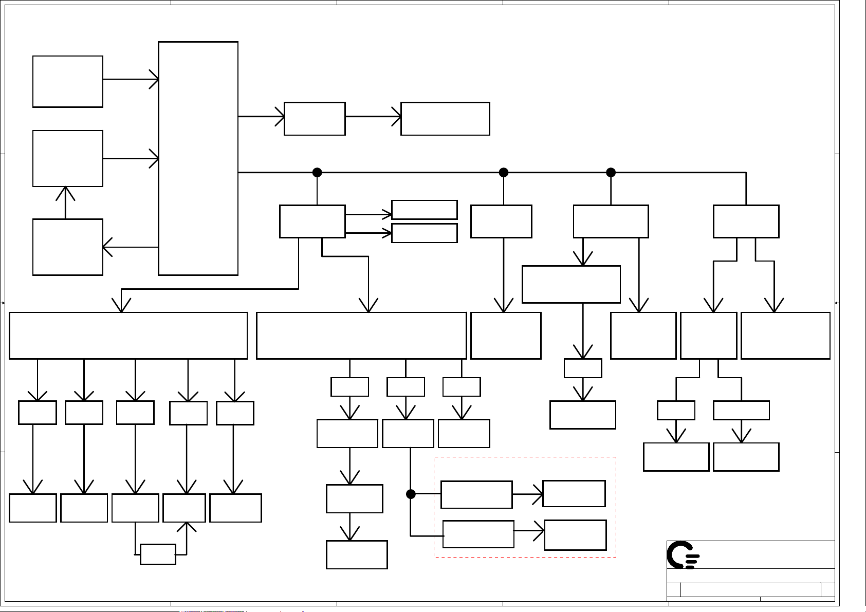
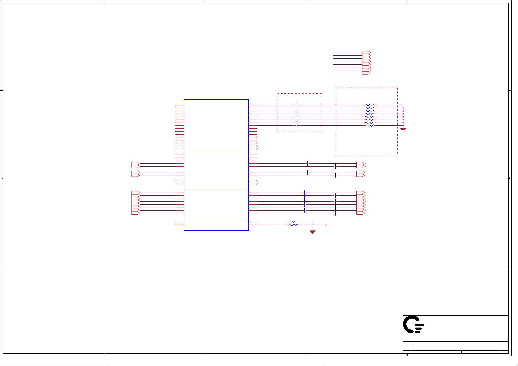
SYSTEM
JX6 MGD-INTEGRATED
RESET CIRCUIT
POWER SW
JX6_PCBJX6_PCB
A A
DDR2-SODIMM1
CH1 DDR II 533/667/800 MHz
PG 17,18
DDR2-SODIMM2
CH2 DDR II 533/667/800 MHz
PG 17,18
DDR2-MEMORY DEVICE
8MX16X4 84-PIN FBGA
PG 16
B B
Panel CONN.
PG 20
CPU HDT
DEBUG PORT
PG 10
533 MHZ DDR II
LVDS
AMD S1
Turion 64 Rev.F Dual-Core/
Sempron Rev.F Single-Core
Dual-Core 35W / Single-Core 25W
(638 S1g1 socket)
PG 8,9,10,11
HT_LINK
RS690
465 FCBGA
PG 12,13,14,15,16
VGA
DVI
PCIE(L2)
TVOUT
PCIE(L1)
CLOCK
ICS951462
PG 7
BCM 5755M
PG 30
MINI-CARD
CRT CONN.
PG 21
WLAN
BATT
CHARGER
AC/BATT
CONNECTOR
E-Switch
PI3L500
+3.3V_LAN
PG 31
PG 43
PG 42
PG 46
PG 51
VGA
DVI
RJ45/Magnetics
PG 31
CPU VR
DC/DC
+3.3V_ALW/+5V_ALW/+15V_ALW
REGULATOR
VCC_NB
REGULATOR
+1.8V_SUS/+1.2V_VCCP
+1.5V_RUN/+0.9V_DDR_VTT
PG 50
PG 47
PG 42
PG 48
PG 35
D-Module
PG 27
SATA - HDD
PG 27
C C
Side External USBX2
USB2.0 (P4)
IDE
SATA
USB2.0 (P0,P1)
SB600
549 BGA
A_LINK
USB2.0 (P6)
PG 33
33MHz PCI
Rear External USBX2
PG 33
USB2.0 (P2,P3)
USB2.0 (P7)
PG 23,24,25,26
LPC
CARDBUS/1394
OZ711EZ1TN
HD-AZALIA
RJ11
for Dock
SPI
PG 32
PG 36
MDC
PG 34
Tip
Ring
PG 34
AUDIO/AMP
STAC9205
PG 28
Audio
Jacks
PG 29
S-Video CONN
PG 22
S/PDIF
USB2.0 (P8)
DOCKING
CONNECTOR
PG 36
Bluetooth
PG 41
D D
FAN & THERMAL
EMC4001
PG 19
1
2
SIO
ECE5018
Expander
USB 2.0 Hub(4)
128 Pins VTQFP
PG 38
Serial Port
PG 33
3
BC
FLASH
SST25VF016B
PG 37
4
EC
MEC5025
128KB Flash
TMKBC
128 Pins VTQFP
PG 39
SPI PS/2
Touchpad/
Stick point
PG 41
BC
Keyboard
Controllor
Keyboard
PG 40
USER
INTERFACE
PG 40
5
ECE1077
PG 37
QUANTA
QUANTA
QUANTA
COMPUTER
COMPUTER
Title
Title
Title
Size Document Number Rev
Size Document Number Rev
Size Document Number Rev
Date: Sheet
Date: Sheet
6
Date: Sheet
COMPUTER
System Block Diagram
System Block Diagram
System Block Diagram
MGD 1A
MGD 1A
MGD 1A
7
of
of
of
289Thursday, March 01, 2007
289Thursday, March 01, 2007
289Thursday, March 01, 2007
8
Page 3
1
2
3
4
5
6
7
8
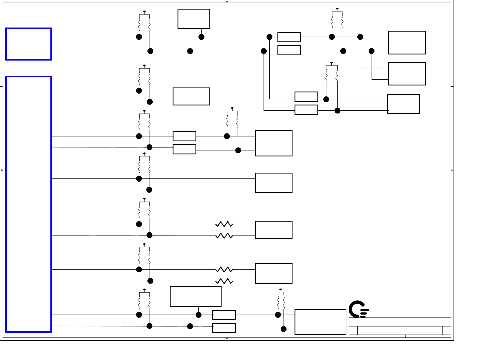
INDEX Power States
Pg# Description
Schematic Block Diagram
1
2
Front Page
3-4
Merom
5-10
Crestline
ICH8M
A A
B B
C C
11-14
DDRII SO-DIMM(200P)
15-16
17
Clock Generator
18-23
VGA
24
LCD Conn. & SSP
25
CRT Conn
26
SATA & IDE Conn
27
PCCARD/Conn & 1394
Express Card & Smart Card
28
29
Mini Card
MDC Conn.
30
31
SIO (MEC5025)
32
SIO (MEC5018)
33
SERIAL PORT & USB
34
Flash ROM, RTC & ECE1077
TP,BT & FIR
35
36
Switch,Keyboard & LED
FAN & Thermal
37
Audio CODEC(STAC9205)/Phone Jack
38-39
LOM (Nineveh)/Switch
40-41
42-43
Docking Conn/Q-Switch
System Reset Circuit
44
Battery Selector & Charger
45-46
47
DDR2_1.8VSUS, 0.9V
48
1.5VSUS,1.05V(VTT)
49
VGA DC/DC,1.25V,1.05V
CPU_MAX8786(3phase)
50
D/D Power
51
52
RUN Power Switch
53
DCIN,Batt
PAD& SCREW
54
55
EMI CAP
SMBUS BLOCK
56
Power Rail S3/M1
+3.3V_ALW
+5V_ALW
+3.3V_LAN
+1.8V_SUS
+0.9V_DDR_VTT
+5V_SUS
+3.3V_SUS
+5V_RUN
+3.3V_RUN
+1.8V_RUN
+1.25V_RUN
+1.5V_RUN
+1.05V_VCCP
VCC_VCRE
+LCDVCC
+5V_MOD
Control
Signal
S0/M0
S3/M1 S4/M1
S3/
M-off
S4/
M-off
S5/
M-off
D D
QUANTA
QUANTA
QUANTA
COMPUTER
COMPUTER
Title
Title
Title
Size Document Number Rev
Size Document Number Rev
Size Document Number Rev
Date: Sheet
Date: Sheet
1
2
3
4
5
6
Date: Sheet
COMPUTER
Index, DNI, Power & Ground
Index, DNI, Power & Ground
Index, DNI, Power & Ground
MGD 1A
MGD 1A
MGD 1A
7
of
of
of
389Thursday, March 01, 2007
389Thursday, March 01, 2007
389Thursday, March 01, 2007
8
Page 4
5
4
3
2
1
POWER STATES
SLP
State
D D
S0 (Full ON)
S3 (Suspend to RAM)
S4 (Suspend to DISK) ON OFF
S5 (SOFT OFF) ON OFFLOW LOW
Signal
SLP
S5#
HIGH
ALWAYS
PLANE
S3#
HIGH
LOW HIGH ON ON OFF
LOW HIGH
ON
SUS
RUN
PLANE
PLANE
ON ON ON
OFF
OFF
CLOCKS
OFF
OFF
OFF
SB600
USB PORT#
0
1
2
3
4
DESTINATION
Side Pair Top
Side Pair Bottom
Rear Bottom as viewed from the back
Rear Top as viewed from the back
Floppy Disk
5
6
7
C C
B B
PM TABLE
State
S0
S3
S5 S4/AC
S5 S4 on Battery
power
plane
+15V_ALW
+5V_ALW
+3.3V_ALW
+1.2V_ALW_SUS
ON
ON
+5V_SUS
+3.3V_SUS
+1.8V_SUS
+0.9V_DDR_VTT
ON ON
ON
OFF
OFFOFF
+5V_RUN
+3.3V_RUN
+2.5V_RUN
+1.8V_RUN
+1.2V_RUN
+1.5V_RUN
+VCC_CORE
+NB_CORE
OFFON
OFF
OFF
ECE5018
8
9
1
2
3
4
PCI EXPRESS
PCI TABLE
PCI DEVICE IDSEL
REQ#/GNT#
PIRQ
Lane 0
Lane 1
Lane 2
MINI CARD-1 WWAN
MINI CARD-2 WLAN
Cardbus
BT
Dock
NC
NC
NC
NC
DESTINATION
LOM
CardBus
A A
5
AD17 REQ#1/GNT#1
REQ#0/GNT#0
4
IRQ_SERIRQ
IRQD
PIRQADocking AD24
3
Lane 3
2
None
QUANTA
QUANTA
QUANTA
COMPUTER
COMPUTER
Title
Title
Title
Size Document Number Rev
Size Document Number Rev
Size Document Number Rev
Date: Sheet
Date: Sheet
Date: Sheet
COMPUTER
ATHLON64 HT I/F
ATHLON64 HT I/F
ATHLON64 HT I/F
MGD 1A
MGD 1A
MGD 1A
1
of
of
of
489Thursday, March 01, 2007
489Thursday, March 01, 2007
489Thursday, March 01, 2007
Page 5
5
4
3
2
1
D D
ADAPTER
+PWR_SRC
FDS4435BZ +INV_PWR_SRC
RUN_ON
BATTERY
ALW_ON
C C
ISL6236
+5V_ALW
MAX8731
+5V_ALW2
+15V_ALW
MAX8774 MAX8632
ISL6236
Charger
1.2V_ALW_SUS_ON
ALW_ON
+5V_ALW
B B
FDC655BN
FDC655BN
SI4810
793475
FDC655BN
+3.3V_ALW
Si4336DY
3.3V_RUN_ON
+3.3V_RUN
ALW_ON
FDS6670AS
ENAB_3VLAN
+3.3V_LAN
FDC655BN
SUS_ON
+3VSUS
+1.2V_ALW_SUS
CPU_VCORE_ENABLE
+VCC_CORE
1.2V_RUN_ON
FDS8880
+1.2V_RUN
NB_VCORE_RUN_ON
+NB_CORE
FDC655BN
1.8V_RUN_ON
DDR_ON
+1.8V_SUS
MAX8794
1.5V_RUN_ON
DDR_ON
+0.9V_DDR_VTT
SUS_ON
HDDC_EN#
MODC_EN#
+5V_HDD +5V_MOD +5V_RUN +VDDA
A A
RUN_ON
AUDIO_AVDD_ENABLE
+5V_SUS
EMC4001
REGCTL_PNP12
PBSS5540Z
( Q40 )
REGCTL_PNP25
MBT35200MT1G
( Q39)
L?
(Option)
5
4
+2.5VRUN
3
5755M
+1.2V_LOM
+2.5V_LOM
2
+1.8V_RUN
Title
Title
Title
ATHLON64 HT I/F
ATHLON64 HT I/F
ATHLON64 HT I/F
Size Document Number Rev
Size Document Number Rev
Size Document Number Rev
MGD 1A
MGD 1A
MGD 1A
Date: Sheet
Date: Sheet
Date: Sheet
+1.5V_RUN
QUANTA
QUANTA
QUANTA
COMPUTER
COMPUTER
COMPUTER
1
of
of
of
589Thursday, March 01, 2007
589Thursday, March 01, 2007
589Thursday, March 01, 2007
Page 6
1
C3
A A
SB600
F3
8
7
B B
13
12
2
3
+3.3V_SUS
2.2K 2.2K
SB_SMBCLK
SB_SMBDATA
+3.3V_ALW
8.2K 8.2K
LCD_SMBCLK
LCD_SMBDAT +3.3V_ALW
+3.3V_ALW
2.2K 2.2K
CKG_SMBCLK
+3.3V_ALWCKG_SMBDAT
+5V_ALW
SMBUS Address [C8]
+3.3V_SUS
6
5
Inverter
2N7002
2N7002
4
5755M
LOM
C8C7
INV
CLK_SCLK
CLK_SDATA
SMBUS Address [58]
+3.3V_RUN
2.2K 2.2K
16
17
5
CLK GEN.
6
2N7002
2N7002
MEM_SCLK
MEM_SDATA
2.2K 2.2K
2N7002
2N7002
SMBUS Address [D2]
+3.3V_RUN
2.2K 2.2K
+3.3V_WLAN
WLAN_SMBCLK
WLAN_SMBDATA
7
197
195
SMBUS Address [A0]
197
195
SMBUS Address [A2]
30
32
SMBUS Address [TBD]
8
DIMM0
DIMM1
WLAN
8.2K 8.2K
SIO
DOCK_SMB_CLK
6
DOCK_SMB_DAT
5
+5V_ALW
39
DOCKING
40
SMBUS Address [C4, 72, 70, 48]
+3.3V_ALW
Macallan IV
C C
10
SBAT_DH_SMBCLK
9
2.2K 2.2K
+3.3V_ALW
100
+3.3V_ALWSBAT_DH_SMBDAT
3
2'nd
4
BATTERY
SMBUS Address [16]
100
2.2K2.2K
112
111
PBAT_SMBCLK
PBAT_SMBDAT
+3.3V_ALW
+3.3V_ALW
D D
100
THERM_SMBCLK
99
1
2
4.7K 4.7K
+3.3V_ALWTHERM_SMBDAT
3
CHARGER
SMBUS Address [12]
910
4
100
100
2N7002
2N7002
3
BATTERY
4
CONN
+3.3V_SUS
2.2K 2.2K
EMC_SMBCLK
EMC_SMBDATA
5
SMBUS Address [16]
12
GUARDIAN
11
SMBUS Address [2F]
6
QUANTA
QUANTA
QUANTA
COMPUTER
COMPUTER
Title
Title
Title
Size Document Number Rev
Size Document Number Rev
Size Document Number Rev
Date: Sheet
Date: Sheet
Date: Sheet
COMPUTER
SMBUS BLOCK
SMBUS BLOCK
SMBUS BLOCK
MGD 1A
MGD 1A
MGD 1A
7
of
of
of
689Thursday, March 01, 2007
689Thursday, March 01, 2007
689Thursday, March 01, 2007
8
Page 7
1
33 ohm +-25%@100MHz
25m ohm max DC resistance
3A current rating
+3.3V_RUN
L27
L27
1 2
BLM18PG330SN1B
BLM18PG330SN1B
12
C599
C599
10U
10U
10
10
X5R
X5R
A A
EP
EP
0805
0805
%
%
±20
±20
B B
C C
+3.3V_CLK
12
0603
0603
C125
C125
22U_6.3V_0805
22U_6.3V_0805
+3.3V_RUN
L28
L28
1 2
BLM15AG221SN1D
BLM15AG221SN1D
+3.3V_RUN
Parallel Resonance Crystal
C588 33P
C588 33P
C584 33P
C584 33P
+3.3V_ALW
+3.3V_RUN
SMbus address D2
These are for
backdrive issue.
CKG_SMBDAT39
D D
CKG_SMBCLK39
1
R554
R554
2.2K
2.2K
1 2
+3.3V_ALW
R524
R524
2.2K
2.2K
1 2
3 1
2N7002W-7-F
2N7002W-7-F
R555 0_NCR555 0_NC
1 2
+3.3V_RUN
3 1
2N7002W-7-F
2N7002W-7-F
R517 0_NCR517 0_NC
1 2
50
50
NPO
NPO
50
50
NPO
NPO
2
Q65
Q65
2
Q64
Q64
2
+3.3V_CLK(40 mils)
12
12
12
C133
C133
C166
C166
0.1U_10V
0.1U_10V
0.1U_10V
0.1U_10V
12
12
C128
C128
C591
C591
0.047U
0.047U
2.2U
2.2U
16
16
6.3
6.3
%
%
±10
±10
0603
0603
0603
0603
X5R
X5R
X7R
X7R
L67
L67
1 2
BLM15AG221SN1D
BLM15AG221SN1D
21
Y5
Y5
14.318MHZ
14.318MHZ
20PPM
20PPM
20p
20p
XTALOUT_CLK_C XTALOUT_CLK
Place R535 less than
100mils from Clock Gen.
R553
R553
2.2K
2.2K
1 2
CLK_SDATA
GDS
231
2N7002W-7-F
C169
C169
0.1U_10V
0.1U_10V
+3VS_CLK_VDD48
+3VS_CLK_VDDREF
12
12
C585
C585
2.2U
2.2U
6.3
6.3
0603
0603
X5R
X5R
R516
R516
1M_NC
1M_NC
1 2
R520 0R520 0
1 2
CLOCK_ENABLE#39
12
C129
C129
0.1U_10V
0.1U_10V
C586
C586
0.047U
0.047U
16
16
±10
±10
0603
0603
X7R
X7R
%
%
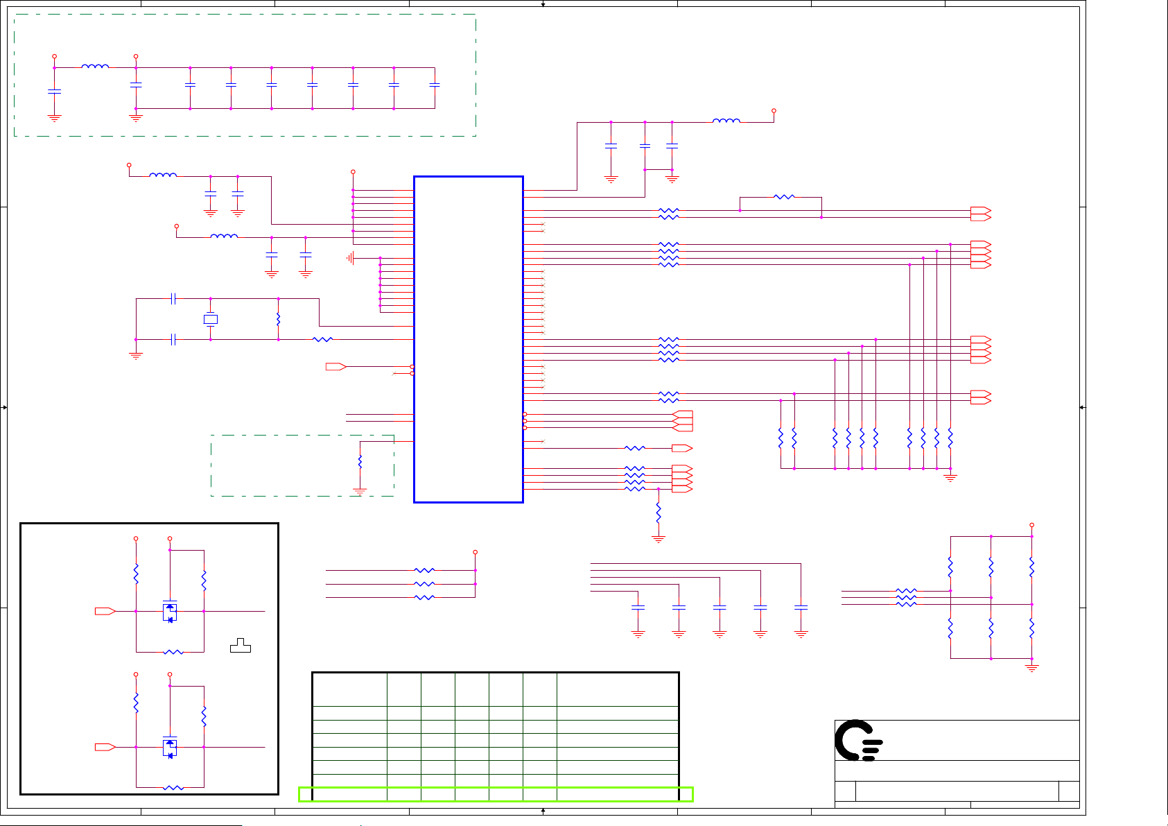
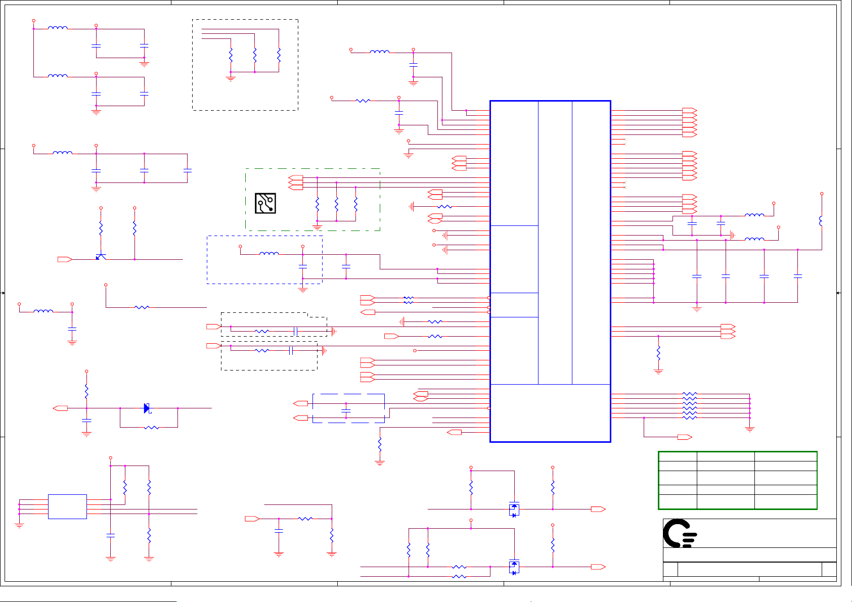
EXT CLK FREQUENCY SELECT TABLE(MHZ)
FS2
R519
1 2
2
R519
2.2K
2.2K
CLK_SCLK
0 0 0
0 0 1
0 1 0
0 1 1
1 0 0
1 0 1
1 1 1
3
12
C174
C174
0.1U_10V
0.1U_10V
+3.3V_CLK
XTALIN_CLK
CLK_SCLK
CLK_SDATA
CLKIREF
R535
R535
475_F
475_F
1 2
LOM_CLKREQ#
MINI1CLK_REQ#
MINI2CLK_REQ#
FS0
FS1
3
12
C137
C137
0.1U_10V
0.1U_10V
U33
U33
54
VDDCPU
14
VDD_SRC1
23
VDD_SRC2
28
VDD_SRC3
44
VDD_SRC4
5
VDD_48
39
VDD_ATIG
2
VDD_REF
60
VDDHTT
53
GND_CPU
15
GND_SRC1
22
GND_SRC2
29
GND_SRC3
45
GND_SRC4
8
GND_48
38
GND_ATIG
1
GND_REF
58
GNDHTT
3
XIN
4
XOUT
11
RESET_IN#
61
NC
9
SMBCLK
10
SMBDAT
48
IREF
ICS951462
ICS951462
R507 10KR507 10K
1 2
R551 10KR551 10K
1 2
R552 10KR552 10K
1 2
CPU
Hi-Z
X
180.00
220.00
100.00
133.33
200.00
12
C179
C179
0.1U_10V
0.1U_10V
SRCCLK
[2:1]
100.00
100.00
100.00
100.00
100.00
100.00
100.00
4
CPUCLK8T0
CPUCLK8C0
CPUCLK8T1
CPUCLK8C1
SRCCLKT6
SRCCLKC6
ATIGCLKT0
ATIGCLKC0
ATIGCLKT1
ATIGCLKC1
ATIGCLKT2
ATIGCLKC2
ATIGCLKT3
ATIGCLKC3
SRCCLKT5
SRCCLKC5
SRCCLKT4
SRCCLKC4
SRCCLKT3
SRCCLKC3
SRCCLKT2
SRCCLKC2
SRCCLKT0
SRCCLKC0
SRCCLKT1
SRCCLKC1
SRCCLKT7
SRCCLKC7
CLKREQA#
CLKREQB#
CLKREQC#
48MHz_1
48MHz_0
FS1/REF1
FS0/REF0
FS2/REF2
HTTCLK0
+3.3V_RUN
PCI
HTT
Hi-Z
Hi-Z
X/3 X/6
60.00
30.00
73.12
36.56
66.66
33.33
33.33
66.66
66.66
33.33 48.00
4
VDDA
GNDA
+3.3V_CLK_VDDA
50
49
CPUCLK_R
56
CPUCLK_R#
55
52
51
PCIE_LOM
16
PCIE_LOM#
17
NB_GFX
41
NB_GFX#
40
37
36
35
34
30
31
18
19
20
21
NB_SBLINK
24
NB_SBLINK#
25
PCIE_MINI2
26
PCIE_MINI2#
27
47
46
43
42
PCIE_SB
12
PCIE_SB#
13
LOM_CLKREQ#
57
32
33
7
CLK_SB
6
FS1
63
FS0
64
FS2
62
HTREFCLK
59
COMMENT
USB
Reserved
48.00
Reserved
48.00
Reserved
48.00
48.00
Reserved
Reserved
48.00
48.00
Reserved
Normal ATHLON64 operation
5
12
12
R526 33R526 33
R514 33R514 33
R511 33R511 33
R117 33R117 33
R523 33R523 33
CLK_SB_48M
CLK_SIO_14M
CLK_NB_14M
CLK_SB_14M
CLK_HTREF_66M
5
C602
C602
C172
C172
0.1U
0.1U
0.047U
0.047U
0402
0402
16
16
%
%
10
10
±10
±10
0603
0603
X7R
X7R
R525 47.5_FR525 47.5_F
1 2
R528 47.5_FR528 47.5_F
1 2
R533 33R533 33
R536 33R536 33
R542 33R542 33
R546 33R546 33
R539 33R539 33
R543 33R543 33
R547 33R547 33
R549 33R549 33
R529 33R529 33
R531 33R531 33
12
C589
C589
10P_NC
10P_NC
50V
50V
220 ohm @100MHz
300mA current rating
12
C603
C603
22U
22U
0805
0805
6.3
6.3
LOM_CLKREQ# 30
MINI2CLK_REQ# 35
MINI1CLK_REQ#
R522
R522
49.9_F
49.9_F
1 2
12
C127
C127
10P_NC
10P_NC
50V
50V
6
L66
L66
BLM15AG221SN1D
BLM15AG221SN1D
CLK_SB_48M 24
CLK_SIO_14M 38
CLK_NB_14M 14
CLK_SB_14M 24
CLK_HTREF_66M 14
12
C580
C580
10P_NC
10P_NC
50V
50V
6
+3.3V_RUN
R527 261_FR527 261_F
1 2
R532 49.9_FR532 49.9_F
R530 49.9_FR530 49.9_F
12
12
12
12
C587
C587
C596
C596
10P_NC
10P_NC
10P_NC
10P_NC
50V
50V
50V
50V
7
R537 49.9_FR537 49.9_F
R544 49.9_FR544 49.9_F
R548 49.9_FR548 49.9_F
R540 49.9_FR540 49.9_F
R550 49.9_FR550 49.9_F
12
12
12
12
FS0
FS1
FS2
Title
Title
Title
CLOCK GENERATOR
CLOCK GENERATOR
CLOCK GENERATOR
Size Document Number Rev
Size Document Number Rev
Size Document Number Rev
MGD 3A
MGD 3A
MGD 3A
Date: Sheet
Date: Sheet
Date: Sheet
12
R518 8.2KR518 8.2K
1 2
R515 8.2KR515 8.2K
1 2
R114 8.2KR114 8.2K
1 2
QUANTA
QUANTA
QUANTA
COMPUTER
COMPUTER
COMPUTER
7
R545 49.9_FR545 49.9_F
R541 49.9_FR541 49.9_F
12
R534 49.9_FR534 49.9_F
12
12
R512
R512
2.2K
2.2K
1 2
R513
R513
2.2K_NC
2.2K_NC
1 2
8
CPU_CLK 10
CPU_CLK# 10
CLK_PCIE_LOM 30
CLK_PCIE_LOM# 30
CLK_NB_GFX 14
CLK_NB_GFX# 14
CLK_NB_SBLINK 14
CLK_NB_SBLINK# 14
CLK_PCIE_MINI2 35
CLK_PCIE_MINI2# 35
CLK_PCIE_SB 23
CLK_PCIE_SB# 23
+3.3V_RUN
R510
R510
2.2K
2.2K
1 2
1 2
R509
R509
2.2K_NC
2.2K_NC
1 2
1 2
of
of
of
789Thursday, March 01, 2007
789Thursday, March 01, 2007
789Thursday, March 01, 2007
8
R113
R113
2.2K
2.2K
R116
R116
2.2K_NC
2.2K_NC
Page 8
5
C502
C101
C101
4.7U
4.7U
10
10
0805
0805
1 2
X7R
D D
X7R
C502
4.7U
4.7U
10
10
0805
0805
1 2
X7R
X7R
C501
C501
4.7U
4.7U
10
10
0805
0805
1 2
X7R
X7R
4
+1.2V_RUN
C95
C95
0.22U
0.22U
10
10
0603
0603
X7R
X7R
C512
C512
0.22U
0.22U
10
10
0603
0603
X7R
X7R
12
C93
C93
180P_50V
180P_50V
12
C518
C518
180P_50V
180P_50V
3
2
1
LAYOUT: Place bypass cap on topside of board
NEAR HT POWER PINS THAT ARE NOT CONNECTED DIRECTLY
TO DOWNSTREAM HT DEVICE, BUT CONNECTED INTERNALLY
TO OTHER HT POWER PINS
PLACE CLOSE TO VLDT0 POWER PINS
PROCESSOR HYPERTRANSPORT INTERFACE
VLDT_Ax AND VLDT_Bx ARE CONNECTED TO THE LDT_RUN POWER
SUPPLY THROUGH THE PACKAGE OR ON THE DIE. IT IS ONLY CONNECTED
ON THE BOARD TO DECOUPLING NEAR THE CPU PACKAGE
C C
HT_CADIN1512
HT_CADIN#1512
HT_CADIN1412
HT_CADIN#1412
HT_CADIN1312
HT_CADIN#1312
HT_CADIN1212
HT_CADIN#1212
HT_CADIN1112
HT_CADIN#1112
HT_CADIN1012
HT_CADIN#1012
HT_CADIN912
HT_CADIN#912
HT_CADIN812
HT_CADIN#812
B B
+1.2V_RUN
R472 51R472 51
A A
R473 51R473 51
HT_CADIN712
HT_CADIN#712
HT_CADIN612
HT_CADIN#612
HT_CADIN512
HT_CADIN#512
HT_CADIN412
HT_CADIN#412
HT_CADIN312
HT_CADIN#312
HT_CADIN212
HT_CADIN#212
HT_CADIN112
HT_CADIN#112
HT_CADIN012
HT_CADIN#012
HT_CLKIN112
HT_CLKIN#112
HT_CLKIN012
HT_CLKIN#012
1 2
1 2
HT_CTLIN012
HT_CTLIN#012
Place R472 and R473 less
than 100mils from CPU
5
+1.2V_RUN
U7AU7A
D4
D3
D2
D1
N5
P5
M3
M4
L5
M5
K3
K4
H3
H4
G5
H5
F3
F4
E5
F5
N3
N2
L1
M1
L3
L2
J1
K1
G1
H1
G3
G2
E1
F1
E3
E2
J5
K5
J3
J2
P3
P4
N1
P1
VLDT_A3
VLDT_A2
VLDT_A1
VLDT_A0
L0_CADIN_H15
L0_CADIN_L15
L0_CADIN_H14
L0_CADIN_L14
L0_CADIN_H13
L0_CADIN_L13
L0_CADIN_H12
L0_CADIN_L12
L0_CADIN_H11
L0_CADIN_L11
L0_CADIN_H10
L0_CADIN_L10
L0_CADIN_H9
L0_CADIN_L9
L0_CADIN_H8
L0_CADIN_L8
L0_CADIN_H7
L0_CADIN_L7
L0_CADIN_H6
L0_CADIN_L6
L0_CADIN_H5
L0_CADIN_L5
L0_CADIN_H4
L0_CADIN_L4
L0_CADIN_H3
L0_CADIN_L3
L0_CADIN_H2
L0_CADIN_L2
L0_CADIN_H1
L0_CADIN_L1
L0_CADIN_H0
L0_CADIN_L0
L0_CLKIN_H1
L0_CLKIN_L1
L0_CLKIN_H0
L0_CLKIN_L0
L0_CTLIN_H1
L0_CTLIN_L1
L0_CTLIN_H0
L0_CTLIN_L0
L0_CADOUT_H15
L0_CADOUT_L15
L0_CADOUT_H14
L0_CADOUT_L14
L0_CADOUT_H13
L0_CADOUT_L13
L0_CADOUT_H12
L0_CADOUT_L12
L0_CADOUT_H11
L0_CADOUT_L11
L0_CADOUT_H10
L0_CADOUT_L10
L0_CADOUT_H9
L0_CADOUT_L9
L0_CADOUT_H8
L0_CADOUT_L8
L0_CADOUT_H7
L0_CADOUT_L7
L0_CADOUT_H6
L0_CADOUT_L6
L0_CADOUT_H5
L0_CADOUT_L5
L0_CADOUT_H4
L0_CADOUT_L4
L0_CADOUT_H3
L0_CADOUT_L3
L0_CADOUT_H2
L0_CADOUT_L2
L0_CADOUT_H1
L0_CADOUT_L1
L0_CADOUT_H0
L0_CADOUT_L0
L0_CLKOUT_H1
L0_CLKOUT_L1
L0_CLKOUT_H0
L0_CLKOUT_L0
L0_CTLOUT_H1
L0_CTLOUT_L1
L0_CTLOUT_H0
L0_CTLOUT_L0
Athlon 64 S1
Processor Socket
4
VLDT_B3
VLDT_B2
VLDT_B1
VLDT_B0
+1.2V_RUN
AE5
AE4
AE3
AE2
T4
T3
V5
U5
V4
V3
Y5
W5
AB5
AA5
AB4
AB3
AD5
AC5
AD4
AD3
T1
R1
U2
U3
V1
U1
W2
W3
AA2
AA3
AB1
AA1
AC2
AC3
AD1
AC1
Y4
Y3
Y1
W1
HT_CPU_CTLOUT1HT_CTLIN1
T5
HT_CPU_CTLOUT#1HT_CTLIN#1
R5
R2
R3
HT_CADOUT15 12
HT_CADOUT#15 12
HT_CADOUT14 12
HT_CADOUT#14 12
HT_CADOUT13 12
HT_CADOUT#13 12
HT_CADOUT12 12
HT_CADOUT#12 12
HT_CADOUT11 12
HT_CADOUT#11 12
HT_CADOUT10 12
HT_CADOUT#10 12
HT_CADOUT9 12
HT_CADOUT#9 12
HT_CADOUT8 12
HT_CADOUT#8 12
HT_CADOUT7 12
HT_CADOUT#7 12
HT_CADOUT6 12
HT_CADOUT#6 12
HT_CADOUT5 12
HT_CADOUT#5 12
HT_CADOUT4 12
HT_CADOUT#4 12
HT_CADOUT3 12
HT_CADOUT#3 12
HT_CADOUT2 12
HT_CADOUT#2 12
HT_CADOUT1 12
HT_CADOUT#1 12
HT_CADOUT0 12
HT_CADOUT#0 12
HT_CLKOUT1 12
HT_CLKOUT#1 12
HT_CLKOUT0 12
HT_CLKOUT#0 12
T97T97
T99T99
HT_CTLOUT0 12
HT_CTLOUT#0 12
Place T97 and T99 less
than 100mils from CPU
3
QUANTA
QUANTA
QUANTA
COMPUTER
COMPUTER
Title
Title
Title
Size Document Number Rev
Size Document Number Rev
Size Document Number Rev
Date: Sheet
Date: Sheet
2
Date: Sheet
COMPUTER
ATHLON64 HT I/F
ATHLON64 HT I/F
ATHLON64 HT I/F
MGD 1A
MGD 1A
MGD 1A
889Thursday, March 01, 2007
889Thursday, March 01, 2007
889Thursday, March 01, 2007
of
of
1
of
Page 9
A
B
C
D
E
Notes for the SODIMM locations:
VDD_VTT_SUS_CPU IS CONNECTED TO THE VDD_VTT_SUS POWER
SUPPLY THROUGH THE PACKAGE OR ON THE DIE. IT IS ONLY CONNECTED
ON THE BOARD TO DECOUPLING NEAR THE CPU PACKAGE
CPU_VTT_SUS_SENSE
should be routed as 10mils
and 10mils spacing from any
4 4
for +0.9V_DDR_VTT
feedback
KEEP TRACE TO RESISTORS LESS
THAN 1.5" FROM CPU PIN
3 3
2 2
1 1
adjacent signals in X, Y, Z
directions.
+1.8V_SUS
R95
R95
39.2
39.2
1%
1%
R100
R100
39.2
39.2
1%
1%
DDR_A_MA[0..15]17,18
DDR_CS3_DIMMA#17,18
DDR_CS2_DIMMA#17,18
DDR_CS1_DIMMA#17,18
DDR_CS0_DIMMA#17,18
DDR_CS3_DIMMB#17,18
DDR_CS2_DIMMB#17,18
DDR_CS1_DIMMB#17,18
DDR_CS0_DIMMB#17,18
DDR_CKE3_DIMMB17,18
DDR_CKE2_DIMMB17,18
DDR_CKE1_DIMMA17,18
DDR_CKE0_DIMMA17,18
CPU_VTT_SUS_SENSE
T113T113
M_ZN
M_ZP
DDR_A_BS217,18
DDR_A_BS117,18
DDR_A_BS017,18
DDR_A_RAS#17,18
DDR_A_CAS#17,18
DDR_A_WE#17,18
+0.9V_CPU_M_VREF_SUS
12
C583
C583
0.1U_10V
0.1U_10V
W17
AE10
AF10
W24
DDR_A_MA15
DDR_A_MA14
DDR_A_MA13
DDR_A_MA12
DDR_A_MA11
DDR_A_MA10
DDR_A_MA9
DDR_A_MA8
DDR_A_MA7
DDR_A_MA6
DDR_A_MA5
DDR_A_MA4
DDR_A_MA3
DDR_A_MA2
DDR_A_MA1
DDR_A_MA0
Y10
V19
J22
V22
T19
Y26
J24
U23
H26
J23
J20
J21
K19
K20
V24
K24
L20
R19
L19
L22
L21
M19
M20
M24
M22
N22
N21
R21
K22
R20
T22
T20
U20
U21
12
C581
C581
0.1U_10V
0.1U_10V
12
C582
C582
1000p_50V
1000p_50V
U7B
U7B
MEMVREF
VTT_SENSE
MEMZN
MEMZP
MA0_CS_L3
MA0_CS_L2
MA0_CS_L1
MA0_CS_L0
MB0_CS_L3
MB0_CS_L2
MB0_CS_L1
MB0_CS_L0
MB_CKE1
MB_CKE0
MA_CKE1
MA_CKE0
MA_ADD15
MA_ADD14
MA_ADD13
MA_ADD12
MA_ADD11
MA_ADD10
MA_ADD9
MA_ADD8
MA_ADD7
MA_ADD6
MA_ADD5
MA_ADD4
MA_ADD3
MA_ADD2
MA_ADD1
MA_ADD0
MA_BANK2
MA_BANK1
MA_BANK0
MA_RAS_L
MA_CAS_L
MA_WE_L
+1.8V_SUS
R508
R508
1K_F_0603
1K_F_0603
1 2
1 2
DDR II: CMD/CTRL/CLK
DDR II: CMD/CTRL/CLK
Athlon 64 S1
Processor Socket
+V_DDR_VREF
1 2
R505 0_0603_NCR505 0_0603_NC
R506
R506
1K_F_0603
1K_F_0603
Place Capacitors for +0.9V_CPU_M_VREF_SUS < 1" from the RS690.
+0.9V_CPU_M_VREF_SUS trace length < 6", trace width > 15mils and
20mils spacing from any adjacent signals in X, Y, Z directions.
+0.9V_DDR_VTT
D10
VTT1
C10
VTT2
B10
VTT3
AD10
VTT4
W10
VTT5
AC10
VTT6
AB10
VTT7
AA10
VTT8
A10
VTT9
Y16
MA0_CLK_H2
AA16
MA0_CLK_L2
E16
MA0_CLK_H1
F16
MA0_CLK_L1
AF18
MB0_CLK_H2
AF17
MB0_CLK_L2
A17
MB0_CLK_H1
A18
MB0_CLK_L1
W23
MB0_ODT1
W26
MB0_ODT0
V20
MA0_ODT1
U19
MA0_ODT0
MB_ADD15
MB_ADD14
MB_ADD13
MB_ADD12
MB_ADD11
MB_ADD10
MB_ADD9
MB_ADD8
MB_ADD7
MB_ADD6
MB_ADD5
MB_ADD4
MB_ADD3
MB_ADD2
MB_ADD1
MB_ADD0
MB_BANK2
MB_BANK1
MB_BANK0
MB_RAS_L
MB_CAS_L
MB_WE_L
DDR_B_MA15
J25
DDR_B_MA14
J26
DDR_B_MA13
W25
DDR_B_MA12
L23
DDR_B_MA11
L25
DDR_B_MA10
U25
DDR_B_MA9
L24
DDR_B_MA8
M26
DDR_B_MA7
L26
DDR_B_MA6
N23
DDR_B_MA5
N24
DDR_B_MA4
N25
DDR_B_MA3
N26
DDR_B_MA2
P24
DDR_B_MA1
P26
DDR_B_MA0
T24
K26
T26
U26
U24
V26
U22
DDR_B_BS2 17,18
DDR_B_BS1 17,18
DDR_B_BS0 17,18
DDR_B_RAS# 17,18
DDR_B_CAS# 17,18
DDR_B_WE# 17,18
M_CLK_DDR1 17
M_CLK_DDR#1 17
M_CLK_DDR0 17
M_CLK_DDR#0 17
M_CLK_DDR3 17
M_CLK_DDR#3 17
M_CLK_DDR2 17
M_CLK_DDR#2 17
M_ODT3 17,18
M_ODT2 17,18
M_ODT1 17,18
M_ODT0 17,18
DDR_B_MA[0..15] 17,18
DIMMA = Far = Bottom
DIMMB = Near = Top
Processor DDR2 Memory Interface
U7C
DDR_B_D[0..63]17
To SODIMM socket B (Near/TOP)
DDR_B_DM[0..7]17 DDR_A_DM[0..7] 17
DDR_B_DQS[0..7]17
DDR_B_DQS#[0..7]17
DDR_B_D63
DDR_B_D62
DDR_B_D61
DDR_B_D60
DDR_B_D59
DDR_B_D58
DDR_B_D57
DDR_B_D56
DDR_B_D55
DDR_B_D54
DDR_B_D53
DDR_B_D52
DDR_B_D51
DDR_B_D50
DDR_B_D49
DDR_B_D48
DDR_B_D47
DDR_B_D46
DDR_B_D45
DDR_B_D44
DDR_B_D43
DDR_B_D42
DDR_B_D41
DDR_B_D40
DDR_B_D39
DDR_B_D38
DDR_B_D37
DDR_B_D36
DDR_B_D35
DDR_B_D34
DDR_B_D33
DDR_B_D32
DDR_B_D31
DDR_B_D30
DDR_B_D29
DDR_B_D28
DDR_B_D27
DDR_B_D26
DDR_B_D25
DDR_B_D24
DDR_B_D23
DDR_B_D22
DDR_B_D21
DDR_B_D20
DDR_B_D19
DDR_B_D18
DDR_B_D17
DDR_B_D16
DDR_B_D15
DDR_B_D14
DDR_B_D13
DDR_B_D12
DDR_B_D11
DDR_B_D10
DDR_B_D9
DDR_B_D8
DDR_B_D7
DDR_B_D6
DDR_B_D5
DDR_B_D4
DDR_B_D3
DDR_B_D2
DDR_B_D1
DDR_B_D0
DDR_B_DQS7
DDR_B_DQS#7
DDR_B_DQS6
DDR_B_DQS#6
DDR_B_DQS5
DDR_B_DQS#5
DDR_B_DQS4
DDR_B_DQS#4
DDR_B_DQS3
DDR_B_DQS#3
DDR_B_DQS2
DDR_B_DQS#2
DDR_B_DQS1
DDR_B_DQS#1
DDR_B_DQS0
DDR_B_DQS#0
DDR_B_DQS0
DDR_B_DQS1
DDR_B_DQS2
DDR_B_DQS3
DDR_B_DQS4
DDR_B_DQS5
DDR_B_DQS6
DDR_B_DQS7
DDR_B_DQS#0
DDR_B_DQS#1
DDR_B_DQS#2
DDR_B_DQS#3
DDR_B_DQS#4
DDR_B_DQS#5
DDR_B_DQS#6
DDR_B_DQS#7
DDR_B_DM7
DDR_B_DM6
DDR_B_DM5
DDR_B_DM4
DDR_B_DM3
DDR_B_DM2
DDR_B_DM1
DDR_B_DM0
AD11
AF11
AF14
AE14
AB11
AC12
AF13
AF15
AF16
AC18
AF19
AD14
AC14
AE18
AD18
AD20
AC20
AF23
AF24
AF20
AE20
AD22
AC22
AE25
AD26
AA25
AA26
AE24
AD24
AA23
AA24
AD12
AC16
AE22
AB26
AF12
AE12
AE16
AD16
AF21
AF22
AC25
AC26
Y11
G24
G23
D26
C26
G26
G25
E24
E23
C24
B24
C20
B20
C25
D24
A21
D20
D18
C18
D14
C14
A20
A19
A16
A15
A13
D12
E11
G11
B14
A14
A11
C11
E25
A22
B16
A12
F26
E26
A24
A23
D16
C16
C12
B12
U7C
MB_DATA63
MB_DATA62
MB_DATA61
MB_DATA60
MB_DATA59
MB_DATA58
MB_DATA57
MB_DATA56
MB_DATA55
MB_DATA54
MB_DATA53
MB_DATA52
MB_DATA51
MB_DATA50
MB_DATA49
MB_DATA48
MB_DATA47
MB_DATA46
MB_DATA45
MB_DATA44
MB_DATA43
MB_DATA42
MB_DATA41
MB_DATA40
MB_DATA39
MB_DATA38
MB_DATA37
MB_DATA36
MB_DATA35
MB_DATA34
MB_DATA33
MB_DATA32
MB_DATA31
MB_DATA30
MB_DATA29
MB_DATA28
MB_DATA27
MB_DATA26
MB_DATA25
MB_DATA24
MB_DATA23
MB_DATA22
MB_DATA21
MB_DATA20
MB_DATA19
MB_DATA18
MB_DATA17
MB_DATA16
MB_DATA15
MB_DATA14
MB_DATA13
MB_DATA12
MB_DATA11
MB_DATA10
MB_DATA9
MB_DATA8
MB_DATA7
MB_DATA6
MB_DATA5
MB_DATA4
MB_DATA3
MB_DATA2
MB_DATA1
MB_DATA0
MB_DM7
MB_DM6
MB_DM5
MB_DM4
MB_DM3
MB_DM2
MB_DM1
MB_DM0
MB_DQS_H7
MB_DQS_L7
MB_DQS_H6
MB_DQS_L6
MB_DQS_H5
MB_DQS_L5
MB_DQS_H4
MB_DQS_L4
MB_DQS_H3
MB_DQS_L3
MB_DQS_H2
MB_DQS_L2
MB_DQS_H1
MB_DQS_L1
MB_DQS_H0
MB_DQS_L0
MA_DATA63
MA_DATA62
MA_DATA61
MA_DATA60
MA_DATA59
MA_DATA58
MA_DATA57
MA_DATA56
MA_DATA55
MA_DATA54
MA_DATA53
MA_DATA52
MA_DATA51
MA_DATA50
MA_DATA49
MA_DATA48
MA_DATA47
MA_DATA46
MA_DATA45
MA_DATA44
MA_DATA43
MA_DATA42
MA_DATA41
MA_DATA40
MA_DATA39
MA_DATA38
MA_DATA37
MA_DATA36
MA_DATA35
MA_DATA34
MA_DATA33
MA_DATA32
MA_DATA31
MA_DATA30
MA_DATA29
MA_DATA28
MA_DATA27
MA_DATA26
MA_DATA25
MA_DATA24
MA_DATA23
MA_DATA22
MA_DATA21
MA_DATA20
MA_DATA19
MA_DATA18
MA_DATA17
MA_DATA16
MA_DATA15
MA_DATA14
MA_DATA13
MA_DATA12
MA_DATA11
MA_DATA10
MA_DQS_H7
MA_DQS_L7
MA_DQS_H6
MA_DQS_L6
MA_DQS_H5
MA_DQS_L5
MA_DQS_H4
MA_DQS_L4
MA_DQS_H3
MA_DQS_L3
MA_DQS_H2
MA_DQS_L2
MA_DQS_H1
MA_DQS_L1
MA_DQS_H0
MA_DQS_L0
Athlon 64 S1
Processor Socket
MA_DATA9
MA_DATA8
MA_DATA7
MA_DATA6
MA_DATA5
MA_DATA4
MA_DATA3
MA_DATA2
MA_DATA1
MA_DATA0
MA_DM7
MA_DM6
MA_DM5
MA_DM4
MA_DM3
MA_DM2
MA_DM1
MA_DM0
DDR: DATA
DDR: DATA
AA12
AB12
AA14
AB14
W11
Y12
AD13
AB13
AD15
AB15
AB17
Y17
Y14
W14
W16
AD17
Y18
AD19
AD21
AB21
AB18
AA18
AA20
Y20
AA22
Y22
W21
W22
AA21
AB22
AB24
Y24
H22
H20
E22
E21
J19
H24
F22
F20
C23
B22
F18
E18
E20
D22
C19
G18
G17
C17
F14
E14
H17
E17
E15
H15
E13
C13
H12
H11
G14
H14
F12
G12
Y13
AB16
Y19
AC24
F24
E19
C15
E12
W12
W13
Y15
W15
AB19
AB20
AD23
AC23
G22
G21
C22
C21
G16
G15
G13
H13
DDR_A_D63
DDR_A_D62
DDR_A_D61
DDR_A_D60
DDR_A_D59
DDR_A_D58
DDR_A_D57
DDR_A_D56
DDR_A_D55
DDR_A_D54
DDR_A_D53
DDR_A_D52
DDR_A_D51
DDR_A_D50
DDR_A_D49
DDR_A_D48
DDR_A_D47
DDR_A_D46
DDR_A_D45
DDR_A_D44
DDR_A_D43
DDR_A_D42
DDR_A_D41
DDR_A_D40
DDR_A_D39
DDR_A_D38
DDR_A_D37
DDR_A_D36
DDR_A_D35
DDR_A_D34
DDR_A_D33
DDR_A_D32
DDR_A_D31
DDR_A_D30
DDR_A_D29
DDR_A_D28
DDR_A_D27
DDR_A_D26
DDR_A_D25
DDR_A_D24
DDR_A_D23
DDR_A_D22
DDR_A_D21
DDR_A_D20
DDR_A_D19
DDR_A_D18
DDR_A_D17
DDR_A_D16
DDR_A_D15
DDR_A_D14
DDR_A_D13
DDR_A_D12
DDR_A_D11
DDR_A_D10
DDR_A_D9
DDR_A_D8
DDR_A_D7
DDR_A_D6
DDR_A_D5
DDR_A_D4
DDR_A_D3
DDR_A_D2
DDR_A_D1
DDR_A_D0
DDR_A_DM7
DDR_A_DM6
DDR_A_DM5
DDR_A_DM4
DDR_A_DM3
DDR_A_DM2
DDR_A_DM1
DDR_A_DM0
DDR_A_DQS7
DDR_A_DQS#7
DDR_A_DQS6
DDR_A_DQS#6
DDR_A_DQS5
DDR_A_DQS#5
DDR_A_DQS4
DDR_A_DQS#4
DDR_A_DQS3
DDR_A_DQS#3
DDR_A_DQS2
DDR_A_DQS#2
DDR_A_DQS1
DDR_A_DQS#1
DDR_A_DQS0
DDR_A_DQS#0
DDR_A_DQS[0..7]17
DDR_A_DQS#[0..7]17
DDR_A_D[0..63] 17
DDR_A_DQS0
DDR_A_DQS1
DDR_A_DQS2
DDR_A_DQS3
DDR_A_DQS4
DDR_A_DQS5
DDR_A_DQS6
DDR_A_DQS7
DDR_A_DQS#0
DDR_A_DQS#1
DDR_A_DQS#2
DDR_A_DQS#3
DDR_A_DQS#4
DDR_A_DQS#5
DDR_A_DQS#6
DDR_A_DQS#7
To SODIMM socket A (Far/Bottom)
QUANTA
QUANTA
QUANTA
COMPUTER
COMPUTER
Title
Title
Title
Size Document Number Rev
Size Document Number Rev
Size Document Number Rev
Date: Sheet
Date: Sheet
A
B
C
D
Date: Sheet
COMPUTER
ATHLON64 DDRII MEMORY
ATHLON64 DDRII MEMORY
ATHLON64 DDRII MEMORY
MGD 1A
MGD 1A
MGD 1A
E
989Thursday, March 01, 2007
989Thursday, March 01, 2007
989Thursday, March 01, 2007
of
of
of
Page 10
5
4
3
2
1
SB600 ONLY
CPU_PWRGD23
D D
LDT_STOP#14,23
C C
CPU_CLK7
CPU_CLK#7
B B
R499
R499
680
680
NOTE: R499 and C564 close to
JCPU pin F10
LDT_RST#23
C115 3900P_50VC115 3900P_50V
1 2
C111 3900P_50VC111 3900P_50V
1 2
1.KEEP TRACE TO RESISTOR LESS THAN 600MILS FROM CPU
PIN AND TRACE TO AC CAPS LESS THAN 1250MILS.
2. CPUCLK and CPUCLK# mismatch < 35 mils.
CPU_PROCHOT#
+1.8V_SUS
R85
R85
680
680
12
R485
R485
10K
10K
CPU_PWRGD
D31
D31
SDMK0340L-7-F
SDMK0340L-7-F
R668 20K
R668 20K
C564
C564
0.1U_16V_NC
0.1U_16V_NC
R88
R88
NOTE: Place R88 on the top of the board that is
680
680
iaccessible, and that shorting across this
resistor will toggle the hyper Transport reset
signal.
12
R91
R91
169_F
169_F
+1.8V_SUS
+3.3V_SUS
12
R479
R479
4.7K
4.7K
1 2
2
Q61
Q61
MMBT3904
MMBT3904
13
EC_CPU_PROCHOT# 39
1%
1%
C760
C760
47P
47P
NPO
NPO
50
50
LDT_RST#
CPU_CLKIN_SC_P
CPU_CLKIN_SC_N
R498 0_NCR498 0_NC
1 2
+1.8V_SUS+1.8V_RUN
R666
R666
0_NC
0_NC
U35
U35
2 4
NL17SZ17DFT2G
NL17SZ17DFT2G
3 5
R6670R667
0
LDT_STOP_R#LDT_STOP_R#
R669
R669
680_NC
680_NC
L65 ferrite bead with an approximate
impedance of 33 , a maximum DC
resistance of 0.025 ohm , and a current
rating of at least 3000mA.
+2.5V_RUN
12
C130
C130
+
+
100U
100U
6.3
6.3
3528
3528
Polymer
Polymer
±20
If AMD SI is not used, the SID pin can be left unconnected
and SIC should have a 300-Ω (±5%) pulldown to VSS.
Place R78 and R77 < 1.5".
Route CPU_HTREF1/0 with 5mils trace width and 10mils
spacing from other signals in X, Y, Z directions
CPU_TEST27_SINGLECHAIN
CPU_TEST26_BURNIN#
CPU_PRESENT#
CPU_TEST25_H_BYPASSCLK_H
CPU_TEST21_SCANEN
CPU_TEST20_SCANCLK2
CPU_TEST24_SCANCLK1
CPU_TEST22_SCANSHIFTEN
CPU_TEST12_SCANSHIFTENB
CPU_TEST15_BP1
CPU_TEST14_BP0
CPU_TEST25_L_BYPASSCLK_L
CPU_TEST19_PLLTEST0
CPU_TEST18_PLLTEST1
If no use which Net
need pull-up or down
±20
To Power
R90 300_NCR90 300_NC
1 2
R86 300R86 300
1 2
R477 1K_FR477 1K_F
1 2
R497 510 1%R497 510 1%
R491 300R491 300
1 2
R84 300_NCR84 300_NC
1 2
R87 300_NCR87 300_NC
1 2
R92 300_NCR92 300_NC
1 2
R487 300_NCR487 300_NC
1 2
R480 300_NCR480 300_NC
1 2
R481 300_NCR481 300_NC
1 2
R484 510 1%R484 510 1%
R482 300R482 300
1 2
R483 300R483 300
1 2
L65
0603L65
0603
12
BLM18PG330SN1D
BLM18PG330SN1D
%
%
CPU_VDD_RUN_FB_H50
CPU_VDD_RUN_FB_L50
T117T117
T114T114
T31T31
T32T32
T115T115
T111T111
LAYOUT: ROUTE VDDA TRACE APPROX.
50 mils WIDE (USE 2x25 mil TRACES TO
EXIT BALL FIELD) AND 500 mils LONG.
This trace should be kept at least 20 mils away from all other signals.
+2.5V_CPU_VDDA_RUN
+2.5V_CPU_VDDA_RUN
12
C526
C526
4.7U
4.7U
10
10
1 2
0805
0805
X7R
X7R
CPU_VDDIO_SUS_FB_H
CPU_VDDIO_SUS_FB_L
CPU_CLK
CPU_CLK#
CPU_TEST29_H_FBCLKOUT_P
CPU_TEST29_L_FBCLKOUT_N
+1.8V_SUS
+2.5V_CPU_VDDA_RUN
C525
C525
0.22U
0.22U
10
10
0603
0603
X7R
X7R
C536
C536
3300P
3300P
50
50
%
%
±5
±5
1 2
LF (Lead Free)
LF (Lead Free)
0402
0402
X7R
X7R
The AMD SI feature has errata, and will not be plemented.
+1.2V_RUN
CPU_VDDIO_SUS_FB_H
CPU_VDDIO_SUS_FB_L
H_THERMDC19
H_THERMDA19
R80 300R80 300
R81 0_NCR81 0_NC
R78 44.2_FR78 44.2_F
1 2
R77 44.2_FR77 44.2_F
1 2
CPU_TEST25_H_BYPASSCLK_H
T119T119
CPU_TEST25_L_BYPASSCLK_L
T110T110
CPU_TEST19_PLLTEST0
T118T118
CPU_TEST18_PLLTEST1
T116T116
CPU_TEST17_BP3
T25T25
CPU_TEST16_BP2
T108T108
CPU_TEST15_BP1
T102T102
CPU_TEST14_BP0
T104T104
CPU_TEST12_SCANSHIFTENB
T106T106
1 2
Place C32< 100mils from CPU.
CPU_RSVD_MA0_CLK3_P
T134T134
CPU_RSVD_MA0_CLK3_N
T124T124
CPU_RSVD_MA0_CLK0_P
T129T129
CPU_RSVD_MA0_CLK0_N
T128T128
CPU_RSVD_MB0_CLK3_P
T130T130
CPU_RSVD_MB0_CLK3_N
T131T131
CPU_RSVD_MB0_CLK0_P
T122T122
CPU_RSVD_MB0_CLK0_N
T126T126
1 2
1 2
T103T103
T105T105
CPU_CLKIN_SC_P
CPU_CLKIN_SC_N
CPU_DBRDY
CPU_TMS
CPU_TCK
CPU_TRST#
CPU_TDI
C531
C531
220P
220P
50V
50V
LDT_RST#
CPU_PWRGD
LDT_STOP_R#
CPU_HTREF1
CPU_HTREF0
H_THERMDC
H_THERMDA
CPU_SIC
CPU_SID
F8
F9
B7
A7
F10
AF4
AF5
P6
R6
F6
E6
W9
Y9
A9
A8
G10
AA9
AC9
AD9
AF9
E9
E8
G9
H10
AA7
C2
D7
E7
F7
C7
AC8
C3
AA6
W7
W8
Y6
AB6
P20
P19
N20
N19
R26
R25
P22
R22
U7D
U7D
VDDA2
VDDA1
RESET_L
PWROK
LDTSTOP_L
SIC
SID
HT_REF1
HT_REF0
VDD_FB_H
VDD_FB_L
VDDIO_FB_H
VDDIO_FB_L
CLKIN_H
CLKIN_L
DBRDY
TMS
TCK
TRST_L
TDI
TEST25_H
TEST25_L
TEST19
TEST18
TEST13
TEST9
TEST17
TEST16
TEST15
TEST14
TEST12
TEST7
TEST6
TEST5
TEST4
TEST3
TEST2
RSVD0
RSVD1
RSVD2
RSVD3
RSVD4
RSVD5
RSVD6
RSVD7
MISC
MISC
THERMTRIP_L
PROCHOT_L
CPU_PRESENT_L
PSI_L
DBREQ_L
TEST29_H
TEST29_L
TEST24
TEST23
TEST22
TEST21
TEST20
TEST28_H
TEST28_L
TEST27
TEST26
TEST10
TEST8
RSVD8
RSVD9
RSVD10
RSVD11
RSVD12
RSVD13
RSVD14
RSVD15
RSVD16
RSVD17
RSVD18
RSVD19
RSVD20
+1.8V_SUS
R478
R478
R486
R486
300
300
300
300
1 2
H_THERMTRIP#
AF6
CPU_PROCHOT#
AC7
A5
VID5
C6
VID4
A6
VID3
A4
VID2
C5
VID1
B5
VID0
AC6
A3
PSI_L is a Power Status Indicator signal. This signal is asserted when the
processor is in a low powerstate. PSI_L should be connected to the power
supply controller, if the controller supports “skipmode, or diode emulation
mode”. PSI_L is asserted by the processor during the C3 and S1 states.
E10
AE9
TDO
CPU_TEST29_H_FBCLKOUT_P
C9
CPU_TEST29_L_FBCLKOUT_N
C8
AE7
AD7
AE8
AB8
AF7
J7
H8
AF8
AE6
K8
C4
H16
B18
B3
C1
H6
G6
D5
R24
W18
R23
AA8
H18
H19
1 2
CPU_PRESENT#
T24T24
CPU_DBREQ#
CPU_TDO
CPU_TEST24_SCANCLK1
CPU_TEST23_TSTUPD
CPU_TEST22_SCANSHIFTEN
CPU_TEST21_SCANEN
CPU_TEST20_SCANCLK2
CPU_TEST27_SINGLECHAIN
CPU_TEST26_BURNIN#
CPU_MA_RESET#
CPU_MB_RESET#
CPU_RSVD_VIDSTRB1
CPU_RSVD_VIDSTRB0
CPU_RSVD_VDDNB_FB_P
CPU_RSVD_VDDNB_FB_N
CPU_RSVD_CORE_TYPE
CPU_RSVD_15
CPU_RSVD_16
CPU_RSVD_17
CPU_RSVD_18
CPU_RSVD_19
CPU_RSVD_20
H_THERMTRIP# 19
VID5 50
VID4 50
VID3 50
VID2 50
VID1 50
VID0 50
CPU_PSI# 50
R490 80.6_FR490 80.6_F
ROUTE AS 80 Ohm DIFFERENTIAL PAIR
PLACE IT CLOSE TO CPU WITHIN 1"
12
T29T29
T109T109
T30T30
T112T112
T27T27
T28T28
T26T26
T120T120
T123T123
T22T22
T23T23
T98T98
T100T100
T101T101
T133T133
T121T121
T132T132
T107T107
T125T125
T127T127
AMD NPT S1 SOCKET
12
12
12
12
12
R98 220_NCR98 220_NC
R101 220_NCR101 220_NC
R492 220_NCR492 220_NC
CPU_DBREQ#
CPU_DBRDY
CPU_TCK
CPU_TMS
CPU_TDI
CPU_TRST#
CPU_TDO
A A
+1.8V_SUS
R494 220_NCR494 220_NC
NOTE:HDT TERMINATION IS REQUIRED FOR REV.Ax SILICON ONLY.
R493 220_NCR493 220_NC
5
HDT CONNECTOR
JHDT1
JHDT1
GND1GND
Resreved13GND
Resreved25GND
DBREQ_L7GND
DBRDY9GND
TCK11GND
TMS13GND
15
TDI
GND
TRST_L17GND
TDO19GND
VDDIO121GND
VDDIO223RESET_L
GND
HDT conn_NC
HDT conn_NC
2
4
6
8
10
12
14
16
18
20
22
24
25
12
12
R64
R64
4.7K
4.7K
R66
R66
100K_NC
100K_NC
+1.8V_RUN+3.3V_RUN
MMBT3904
MMBT3904
12
R67
R67
4.7K
4.7K
2
Q13
Q13
LDT_RST#CPU_RESET#
13
4
3
Processor Socket
QUANTA
QUANTA
QUANTA
COMPUTER
COMPUTER
Title
Title
Title
Size Document Number Rev
Size Document Number Rev
Size Document Number Rev
Date: Sheet
Date: Sheet
2
Date: Sheet
COMPUTER
ATHLON64 CTRL & DEBUG
ATHLON64 CTRL & DEBUG
ATHLON64 CTRL & DEBUG
MGD 3A
MGD 3A
MGD 3A
1
10 89Thursday, March 01, 2007
10 89Thursday, March 01, 2007
10 89Thursday, March 01, 2007
of
of
of
Page 11
5
4
3
2
1
+VCC_CORE
C539
C539
U7F
+VCC_CORE +VCC_CORE
D D
C C
B B
A1
AC4
AD2
M10
N11
R11
U11
U13
G4
H2
J9
J11
J13
K6
K10
K12
K14
L4
L7
L9
L11
L13
M2
M6
M8
N7
N9
P8
P10
R4
R7
R9
T2
T6
T8
T10
T12
T14
U7
U9
V6
V8
V10
U7E
U7E
VDD1
VDD2
VDD3
VDD4
VDD5
VDD6
VDD7
VDD8
VDD9
VDD10
VDD11
VDD12
VDD13
VDD14
VDD15
VDD16
VDD17
VDD18
VDD19
VDD20
VDD21
VDD22
VDD23
VDD24
VDD25
VDD26
VDD27
VDD28
VDD29
VDD30
VDD31
VDD32
VDD33
VDD34
VDD35
VDD36
VDD37
VDD38
VDD39
VDD40
VDD41
VDD42
POWER
POWER
Athlon 64 S1
Processor Socket
VDD43
VDD44
VDD45
VDD46
VDD47
VDD48
VDD49
VDD50
VDD51
VDD52
VDD53
VDD54
VDDIO1
VDDIO2
VDDIO3
VDDIO4
VDDIO5
VDDIO6
VDDIO7
VDDIO8
VDDIO9
VDDIO10
VDDIO11
VDDIO12
VDDIO13
VDDIO14
VDDIO15
VDDIO16
VDDIO17
VDDIO18
VDDIO19
VDDIO20
VDDIO21
VDDIO22
VDDIO23
VDDIO24
VDDIO25
VDDIO26
VDDIO27
V12
V14
W4
Y2
J15
K16
L15
M16
P16
T16
U15
V16
H25
J17
K18
K21
K23
K25
L17
M18
M21
M23
M25
N17
P18
P21
P23
P25
R17
T18
T21
T23
T25
U17
V18
V21
V23
V25
Y25
+1.8V_SUS
A26
AA4
AA11
AA13
AA15
AA17
AA19
AB2
AB7
AB9
AB23
AB25
AC11
AC13
AC15
AC17
AC19
AC21
AD6
AD8
AD25
AE11
AE13
AE15
AE17
AE19
AE21
AE23
B11
B13
B15
B17
B19
B21
B23
B25
D11
D13
D15
D17
D19
D21
D23
D25
H21
H23
F11
F13
F15
F17
F19
F21
F23
F25
B4
B6
B8
B9
D6
D8
D9
E4
F2
H7
H9
J4
U7F
VSS1
VSS2
VSS3
VSS4
VSS5
VSS6
VSS7
VSS8
VSS9
VSS10
VSS11
VSS12
VSS13
VSS14
VSS15
VSS16
VSS17
VSS18
VSS19
VSS20
VSS21
VSS22
VSS23
VSS24
VSS25
VSS26
VSS27
VSS28
VSS29
VSS30
VSS31
VSS32
VSS33
VSS34
VSS35
VSS36
VSS37
VSS38
VSS39
VSS40
VSS41
VSS42
VSS43
VSS44
VSS45
VSS46
VSS47
VSS48
VSS49
VSS50
VSS51
VSS52
VSS53
VSS54
VSS55
VSS56
VSS57
VSS58
VSS59
VSS60
VSS61
VSS62
VSS63
VSS64
VSS65
Athlon 64 S1
Processor Socket
GROUND
GROUND
VSS66
VSS67
VSS68
VSS69
VSS70
VSS71
VSS72
VSS73
VSS74
VSS75
VSS76
VSS77
VSS78
VSS79
VSS80
VSS81
VSS82
VSS83
VSS84
VSS85
VSS86
VSS87
VSS88
VSS89
VSS90
VSS91
VSS92
VSS93
VSS94
VSS95
VSS96
VSS97
VSS98
VSS99
VSS100
VSS101
VSS102
VSS103
VSS104
VSS105
VSS106
VSS107
VSS108
VSS109
VSS110
VSS111
VSS112
VSS113
VSS114
VSS115
VSS116
VSS117
VSS118
VSS119
VSS120
VSS121
VSS122
VSS123
VSS124
VSS125
VSS126
VSS127
VSS128
VSS129
J6
J8
J10
J12
J14
J16
J18
K2
K7
K9
K11
K13
K15
K17
L6
L8
L10
L12
L14
L16
L18
M7
M9
M11
M17
N4
N8
N10
N16
N18
P2
P7
P9
P11
P17
R8
R10
R16
R18
T7
T9
T11
T13
T15
T17
U4
U6
U8
U10
U12
U14
U16
U18
V2
V7
V9
V11
V13
V15
V17
W6
Y21
Y23
N6
1
22U
22U
6.3
6.3
0805
0805
2
X6S
X6S
+VCC_CORE
C557
C557
1
22U
22U
6.3
6.3
0805
0805
2
X6S
X6S
+1.8V_SUS
C566
C566
1
22U
22U
6.3
6.3
0805
0805
2
X6S
X6S
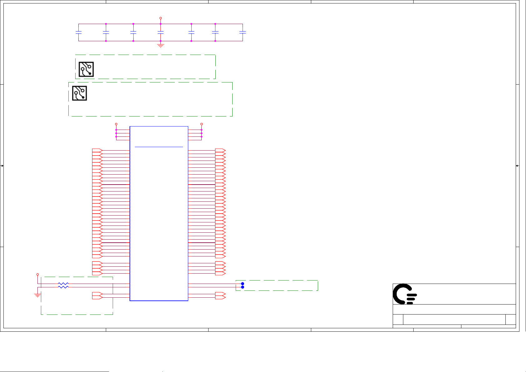
DECOUPLING BETWEEN PROCESSOR AND DIMMs
PLACE CLOSE TO PROCESSOR AS POSSIBLE
+1.8V_SUS
C186
C186
10U
10U
10
10
1 2
0805
0805
X7R
X7R
+1.8V_SUS
12
C594
C594
0.01U_16V
0.01U_16V
C117
C117
4.7U
4.7U
10
10
1 2
0805
0805
X7R
X7R
BOTTOMSIDE DECOUPLING
C538
1 2
C540
C540
4.7U
4.7U
10
10
0805
0805
X7R
X7R
1
2
1
2
1
2
1 2
12
C529
C529
22U
22U
6.3
6.3
0805
0805
X6S
X6S
C554
C554
22U
22U
6.3
6.3
0805
0805
X6S
X6S
C569
C569
22U
22U
6.3
6.3
0805
0805
X6S
X6S
C184
C184
10U
10U
10
10
0805
0805
X7R
X7R
C568 to be
placed as close
as possible to
the socket
C595
C595
0.01U_16V
0.01U_16V
C538
1
22U
22U
6.3
6.3
0805
0805
2
X6S
X6S
C560
C560
0.22U
0.22U
10
10
0603
0603
C571
C571
0.22U
0.22U
10
10
0603
0603
C187
C187
10U
10U
10
10
1 2
0805
0805
X7R
X7R
12
C568
C568
180P_50V
180P_50V
C552
C552
4.7U
4.7U
10
10
1 2
0805
0805
X7R
X7R
1
2
12
+0.9V_DDR_VTT
C121
C121
4.7U
4.7U
10
10
1 2
0805
0805
X7R
X7R
+0.9V_DDR_VTT
C530
C530
22U
22U
6.3
6.3
0805
0805
X6S
X6S
C528
C528
0.22U
0.22U
10
10
0603
0603
C576
C576
0.22U
0.22U
10
10
0603
0603
1 2
C597
C597
180P_50V
180P_50V
C185
C185
10U
10U
10
10
0805
0805
X7R
X7R
1
2
1
2
12
C567
C567
22U_NC
22U_NC
6.3
6.3
0805
0805
X6S
X6S
12
C565
C565
0.22U
0.22U
10
10
0603
0603
X7R
X7R
C550
C550
22U
22U
6.3
6.3
0805
0805
X6S
X6S
C535
C535
0.01U_16V
0.01U_16V
C601
C601
0.22U
0.22U
10
10
0603
0603
X7R
X7R
C598
C598
180P_50V
180P_50V
C549
C549
1
22U
22U
6.3
6.3
0805
0805
2
X6S
X6S
12
C558
C558
180P_50V
180P_50V
C597,and C598 to be
evenly spaced along the
VDDIO/VSS plane split
C544
C544
0.22U
0.22U
10
10
0603
0603
X7R
X7R
1
2
C543
C543
1
22U_NC
22U_NC
6.3
6.3
0805
0805
2
X6S
X6S
22uF/0805/6.3V/X6S
0.22uF/0603/10V/X7R
0.01uF/0402/16V/X7R
180pF/0402/50V/NPO
C593
C593
0.22U
0.22U
10
10
0603
0603
X7R
X7R
C545
C545
22U
22U
6.3
6.3
0805
0805
X6S
X6S
C600
C600
0.22U
0.22U
10
10
0603
0603
X7R
X7R
22uF/0805/6.3V/X6S
10uF/0805/10V/X7R
4.7uF/0805/10V/X7R
0.22uF/0603/10V/X7R
0.01uF/0402/16V/X7R
1000pF/0402/50V/X7R
180pF/0402/50V/NPO
C551
C551
0.22U
0.22U
10
10
0603
0603
X7R
X7R
C555
C555
0.22U
0.22U
10
10
0603
0603
X7R
X7R
C592
C592
0.22U
0.22U
10
10
0603
0603
X7R
X7R
12
C118
Athlon 64 S1g1
uPGA638
A A
Top View
C118
1000p_50V
1000p_50V
12
C546
C546
1000p_50V
1000p_50V
12
C120
C120
1000p_50V
1000p_50V
12
C556
C556
1000p_50V
1000p_50V
12
C119
C119
180P_50V
180P_50V
12
C553
C553
180P_50V
180P_50V
12
C562
C562
180P_50V
180P_50V
AF1
PROCESSOR POWER AND GROUND
5
4
3
2
12
C122
C122
180P_50V
180P_50V
QUANTA
QUANTA
QUANTA
COMPUTER
COMPUTER
Title
Title
Title
Size Document Number Rev
Size Document Number Rev
Size Document Number Rev
Date: Sheet
Date: Sheet
Date: Sheet
COMPUTER
ATHLON64 PWR & GND
ATHLON64 PWR & GND
ATHLON64 PWR & GND
MGD 1A
MGD 1A
MGD 1A
1
of
of
of
11 89Thursday, March 01, 2007
11 89Thursday, March 01, 2007
11 89Thursday, March 01, 2007
Page 12
5
D D
4
3
2
1
Change Part Number
U5A
U5A
Rev.A12
P21
P22
P18
P19
M22
M21
M18
M19
L18
L19
G22
G21
J20
J21
F21
F22
N24
N25
L25
M24
K25
K24
J23
K23
G25
H24
F25
F24
E23
F23
E24
E25
L21
L22
J24
J25
N23
P23
HT_TXCALP
C25
HT_TXCALN
D24
Place R450 < 100 mils from U5A.C25 and U5A.D24
HT_CADIN15 8
HT_CADIN#15 8
HT_CADIN14 8
HT_CADIN#14 8
HT_CADIN13 8
HT_CADIN#13 8
HT_CADIN12 8
HT_CADIN#12 8
HT_CADIN11 8
HT_CADIN#11 8
HT_CADIN10 8
HT_CADIN#10 8
HT_CADIN9 8
HT_CADIN#9 8
HT_CADIN8 8
HT_CADIN#8 8
HT_CADIN7 8
HT_CADIN#7 8
HT_CADIN6 8
HT_CADIN#6 8
HT_CADIN5 8
HT_CADIN#5 8
HT_CADIN4 8
HT_CADIN#4 8
HT_CADIN3 8
HT_CADIN#3 8
HT_CADIN2 8
HT_CADIN#2 8
HT_CADIN1 8
HT_CADIN#1 8
HT_CADIN0 8
HT_CADIN#0 8
HT_CLKIN1 8
HT_CLKIN#1 8
HT_CLKIN0 8
HT_CLKIN#0 8
HT_CTLIN0 8
HT_CTLIN#0 8
R450 100_FR450 100_F
1 2
check
HT_CADOUT158
HT_CADOUT#158
HT_CADOUT148
HT_CADOUT#148
HT_CADOUT138
HT_CADOUT#138
HT_CADOUT128
HT_CADOUT#128
HT_CADOUT118
HT_CADOUT#118
HT_CADOUT108
HT_CADOUT#108
HT_CADOUT98
HT_CADOUT#98
HT_CADOUT88
C C
B B
+VDDHT_PKG
HT_CADOUT#88
HT_CADOUT78
HT_CADOUT#78
HT_CADOUT68
HT_CADOUT#68
HT_CADOUT58
HT_CADOUT#58
HT_CADOUT48
HT_CADOUT#48
HT_CADOUT38
HT_CADOUT#38
HT_CADOUT28
HT_CADOUT#28
HT_CADOUT18
HT_CADOUT#18
HT_CADOUT08
HT_CADOUT#08
HT_CLKOUT18
HT_CLKOUT#18
HT_CLKOUT08
HT_CLKOUT#08
HT_CTLOUT08
HT_CTLOUT#08
R429 49.9_FR429 49.9_F
1 2
R453 49.9_FR453 49.9_F
1 2
HT_RXCALP
HT_RXCALN
R19
R18
R21
R22
U22
U21
U18
U19
W19
W20
AC21
AB22
AB20
AA20
AA19
Y19
T24
R25
U25
U24
V23
U23
V24
V25
AA25
AA24
AB23
AA23
AB24
AB25
AC24
AC25
W21
W22
Y24
W25
P24
P25
A24
C24
HT_RXCAD15P
HT_RXCAD15N
HT_RXCAD14P
HT_RXCAD14N
HT_RXCAD13P
HT_RXCAD13N
HT_RXCAD12P
HT_RXCAD12N
HT_RXCAD11P
HT_RXCAD11N
HT_RXCAD10P
HT_RXCAD10N
HT_RXCAD9P
HT_RXCAD9N
HT_RXCAD8P
HT_RXCAD8N
HT_RXCAD7P
HT_RXCAD7N
HT_RXCAD6P
HT_RXCAD6N
HT_RXCAD5P
HT_RXCAD5N
HT_RXCAD4P
HT_RXCAD4N
HT_RXCAD3P
HT_RXCAD3N
HT_RXCAD2P
HT_RXCAD2N
HT_RXCAD1P
HT_RXCAD1N
HT_RXCAD0P
HT_RXCAD0N
HT_RXCLK1P
HT_RXCLK1N
HT_RXCLK0P
HT_RXCLK0N
HT_RXCTLP
HT_RXCTLN
HT_RXCALP
HT_RXCALN
RS690T
RS690T
PART 1 OF 6
PART 1 OF 6
HT_TXCAD15P
HT_TXCAD15N
HT_TXCAD14P
HT_TXCAD14N
HT_TXCAD13P
HT_TXCAD13N
HT_TXCAD12P
HT_TXCAD12N
HT_TXCAD11P
HT_TXCAD11N
HT_TXCAD10P
HT_TXCAD10N
HT_TXCAD9P
HT_TXCAD9N
HT_TXCAD8P
HT_TXCAD8N
HT_TXCAD7P
HT_TXCAD7N
HT_TXCAD6P
HT_TXCAD6N
HT_TXCAD5P
HT_TXCAD5N
HT_TXCAD4P
HT_TXCAD4N
HT_TXCAD3P
HT_TXCAD3N
HT_TXCAD2P
HT_TXCAD2N
HT_TXCAD1P
HT_TXCAD1N
HT_TXCAD0P
HT_TXCAD0N
HT_TXCLK1P
HT_TXCLK1N
HT_TXCLK0P
HT_TXCLK0N
HT_TXCTLP
HT_TXCTLN
HYPER TRANSPORT CPU I/F
HYPER TRANSPORT CPU I/F
HT_TXCALP
HT_TXCALN
A A
Title
Title
Title
Size Document Number Rev
Size Document Number Rev
Size Document Number Rev
Date: Sheet
Date: Sheet
5
4
3
2
Date: Sheet
QUANTA
QUANTA
QUANTA
COMPUTER
COMPUTER
COMPUTER
RS690T-HT LINK0 I/F
RS690T-HT LINK0 I/F
RS690T-HT LINK0 I/F
MGD 2A
MGD 2A
MGD 2A
12 89Thursday, March 01, 2007
12 89Thursday, March 01, 2007
12 89Thursday, March 01, 2007
of
of
1
of
Page 13
5
4
3
2
1
D D
U5B
U5B
G5
GFX_RX0P
G4
GFX_RX0N
J8
GFX_RX1P
J7
GFX_RX1N
J4
GFX_RX2P
J5
GFX_RX2N
L8
GFX_RX3P
L7
GFX_RX3N
L4
GFX_RX4P
L5
GFX_RX4N
M8
AB7
AB6
AC4
AD4
M7
M4
M5
P8
P7
R7
R8
U4
U5
P4
P5
R4
R5
V9
W9
Y4
Y5
W4
W5
GFX_RX5P
GFX_RX5N
GFX_RX6P
GFX_RX6N
GFX_RX7P
GFX_RX7N
GPP_RX0P
GPP_RX0N
GPP_RX1P
GPP_RX1N
GPP_RX2P
GPP_RX2N
GPP_RX3P
GPP_RX3N
SB_RX0P
SB_RX0N
SB_RX1P
SB_RX1N
SB_RX2P
SB_RX2N
SB_RX3P
SB_RX3N
NC_1
NC_2
RS690T
RS690T
C C
PCIE_NBRX_WLANTX_P135
WLAN <-----
GIGA LAN <-----
B B
PCIE_NBRX_WLANTX_N135
PCIE_NBRX_LOMTX_P230
PCIE_NBRX_LOMTX_N230
ALINK_NBRX_SBTX_P023
ALINK_NBRX_SBTX_N023
ALINK_NBRX_SBTX_P123
ALINK_NBRX_SBTX_N123
ALINK_NBRX_SBTX_P223
ALINK_NBRX_SBTX_N223
ALINK_NBRX_SBTX_P323
ALINK_NBRX_SBTX_N323
PART 2 OF 6
PART 2 OF 6
PCIE I/F
PCIE I/F
GFX
GFX
PCIE I/F GPP
PCIE I/F GPP
PCIE I/F SB
PCIE I/F SB
GFX_TX0P
GFX_TX0N
GFX_TX1P
GFX_TX1N
GFX_TX2P
GFX_TX2N
GFX_TX3P
GFX_TX3N
GFX_TX4P
GFX_TX4N
GFX_TX5P
GFX_TX5N
GFX_TX6P
GFX_TX6N
GFX_TX7P
GFX_TX7N
GPP_TX0P
GPP_TX0N
GPP_TX1P
GPP_TX1N
GPP_TX2P
GPP_TX2N
GPP_TX3P
GPP_TX3N
SB_TX0P
SB_TX0N
SB_TX1P
SB_TX1N
SB_TX2P
SB_TX2N
SB_TX3P
SB_TX3N
PCE_PCAL
PCE_NCAL
Rev.A12
DVI_C_TX2+
J1
DVI_C_TX2-
H2
DVI_C_TX1+
K2
DVI_C_TX1-
K1
DVI_C_TX0+
K3
DVI_C_TX0-
L3
DVI_C_CLK+
L1
DVI_C_CLK-
L2
N2
N1
P2
P1
P3
R3
R1
R2
V3
W3
PCIE_NBTX_WLANRX_P1
W1
PCIE_NBTX_WLANRX_N1
W2
PCIE_NBTX_LOMRX_P2
U2
PCIE_NBTX_LOMRX_N2
U1
V2
V1
ALINK_NBTX_SBRX_P0
AC1
ALINK_NBTX_SBRX_N0
AC2
ALINK_NBTX_SBRX_P1
AB1
ALINK_NBTX_SBRX_N1
AB2
ALINK_NBTX_SBRX_P2
AA1
ALINK_NBTX_SBRX_N2
AA2
ALINK_NBTX_SBRX_P3
Y2
ALINK_NBTX_SBRX_N3
Y3
PCE_PCAL
AE4
PCE_NCAL
AE3
Place near RS690T
C72 0.1U_16VC72 0.1U_16V
1 2
C71 0.1U_16VC71 0.1U_16V
1 2
C80 0.1U_16VC80 0.1U_16V
1 2
C75 0.1U_16VC75 0.1U_16V
1 2
C73 0.1U_16VC73 0.1U_16V
1 2
C74 0.1U_16VC74 0.1U_16V
1 2
C81 0.1U_16VC81 0.1U_16V
1 2
C82 0.1U_16VC82 0.1U_16V
1 2
C85 0.1U
C83 0.1U
C94 0.1U
C91 0.1U
C89 0.1U
C87 0.1U
R83 562_FR83 562_F
1 2
R82 2K_FR82 2K_F
1 2
X7R
X7R
X7R
X7R
X7R
X7R
X7R
X7R
X7R
X7R
X7R
X7R
DVI_TX2+
DVI_TX2DVI_TX1+
DVI_TX1DVI_TX0+
DVI_TX0DVI_CLK+
DVI_CLK-
10C85 0.1U
10
C86 0.1U
10C83 0.1U
10
C84 0.1U
10C94 0.1U
10
C96 0.1U
10C91 0.1U
10
C92 0.1U
10C89 0.1U
10
C90 0.1U
10C87 0.1U
10
C88 0.1U
+1.2V_VDDA12
DVI_TX2+
DVI_TX2-
DVI_TX1+
DVI_TX1-
DVI_TX0+
DVI_TX0DVI_CLK+
DVI_CLK-
No placement limitation,
minimum stub
R454 750 1%R454 750 1%
R452 750 1%R452 750 1%
R465 750 1%R465 750 1%
R460 750 1%R460 750 1%
R73 750 1%R73 750 1%
R74 750 1%R74 750 1%
R75 750 1%R75 750 1%
R76 750 1%R76 750 1%
Layout Note :750 ohm
resistors
are placed at the same
via as
the series capacitors
10C86 0.1U
10
X7R
X7R
10C84 0.1U
10
X7R
X7R
10C96 0.1U
10
X7R
X7R
10C92 0.1U
10
X7R
X7R
10C90 0.1U
10
X7R
X7R
10C88 0.1U
10
X7R
X7R
DVI_TX2+ 36
DVI_TX2- 36
DVI_TX1+ 36
DVI_TX1- 36
DVI_TX0+ 36
DVI_TX0- 36
DVI_CLK+ 36
DVI_CLK- 36
PCIE_NBTX_C_WLANRX_P1 35
PCIE_NBTX_C_WLANRX_N1 35
PCIE_NBTX_C_LOMRX_P2 30
PCIE_NBTX_C_LOMRX_N2 30
ALINK_NBTX_C_SBRX_P0 23
ALINK_NBTX_C_SBRX_N0 23
ALINK_NBTX_C_SBRX_P1 23
ALINK_NBTX_C_SBRX_N1 23
ALINK_NBTX_C_SBRX_P2 23
ALINK_NBTX_C_SBRX_N2 23
ALINK_NBTX_C_SBRX_P3 23
ALINK_NBTX_C_SBRX_N3 23
----->WLAN
----->GIGA LAN
A A
QUANTA
QUANTA
QUANTA
COMPUTER
COMPUTER
Title
Title
Title
Size Document Number Rev
Size Document Number Rev
Size Document Number Rev
Date: Sheet
Date: Sheet
5
4
3
2
Date: Sheet
COMPUTER
RS485-PCIE LINK I/F
RS485-PCIE LINK I/F
RS485-PCIE LINK I/F
MGD 3A
MGD 3A
MGD 3A
1
of
of
of
13 89Thursday, March 01, 2007
13 89Thursday, March 01, 2007
13 89Thursday, March 01, 2007
Page 14
5
+1.8V_RUN
L19
L19
BLM15AG221SN1D
BLM15AG221SN1D
L18
D D
L18
BLM15AG221SN1D
BLM15AG221SN1D
+1.8V_AVDDQ
C52
C52
10U_10V_0805_NC
10U_10V_0805_NC
1 2
+1.8V_PLLVDD
C53
C53
10U_10V_0805_NC
10U_10V_0805_NC
1 2
12
C453
C453
2.2U_10V_0603
2.2U_10V_0603
12
C54
C54
2.2U_10V_0603
2.2U_10V_0603
TV_CVBS
TV_Y
TV_C
R435, R451 and R444
should be placed
close to NB
+1.8V_RUN
BLM15AG221SN1D
BLM15AG221SN1D
C C
LDT_STOP#10,23
+1.2V_VDDA12 +1.2V_PLLVDD12
L53
L53
BLM15AG221SN1D
BLM15AG221SN1D
B B
BMREQ#23
U32
U32
1
NC
2
A1
3
A A
A2
4
VSS
AT24C04N-10SU-2.7_NC
AT24C04N-10SU-2.7_NC
NOTE: ACCESS TO STRAP_DATA and I2C_CLK PINS IS MANDATORY.
L22
L22
+1.8V_HTPVDD
1 3
12
C451
C451
2.2U_10V_0603
2.2U_10V_0603
+3.3V_RUN
1 2
1 2
8
VCC
7
WP
6
SCL
5
SDA
5
C66
C66
10U_10V_0805_NC
10U_10V_0805_NC
1 2
+1.8V_RUN
R47
R47
4.7K
4.7K
1 2
2
Q12
Q12
MMBT3904
MMBT3904
+3.3V_RUN
R441
R441
10K_NC
10K_NC
C466
C466
15P_NC
15P_NC
+3.3V_RUN
12
C64
C64
4.7U_6.3V_0603
4.7U_6.3V_0603
+3.3V_RUN
R49
R49
10K
10K
1 2
LDT_STOP#_NB
R71 4.7KR71 4.7K
1 2
D23
D23
SDMK0340L-7-F_NC
SDMK0340L-7-F_NC
R434 0R434 0
12
R458
R458
R457
R457
10K_NC
10K_NC
2K_NC
2K_NC
1 2
LCD_DDCCLK
NB_VCORE_CNTRL
12
R456
C483
C483
0.1U_NC
0.1U_NC
16
16
R456
2K_NC
2K_NC
12
SUS_STAT#
CLK_HTREF_66M7
CLK_NB_14M7
C68
C68
1U
1U
6.3
6.3
X5R
X5R
BMREQ#_D
DVI_DETECT36
4
12
12
R435
R435
150
150
1%
1%
+1.2V_VDDA12 +1.2V_VDDPLL
12
R451
R451
150
150
1%
1%
VGA_RED21,36
VGA_GRN21,36
VGA_BLU21,36
L58
L58
1 2
BLM21PG221SN1D
BLM21PG221SN1D
0805Imax = 2
0805Imax = 2
R444
R444
150
150
1%
1%
R446,R455,R461 CLOSE TO NB
12
RS690: 220 Ohm 2A FB
AC Term closely clock
pin for length: 50 mils
R433
R433
1 2
22_NC
22_NC
R427
R427
1 2
33 1%
33 1%
AC Term closely clock
pin for length: 50 mils
NB_THERMDA19
NB_THERMDC19
1 2
1 2
C456
C456
22P50 NPO
22P50 NPO
Place C98 < 100mils from RS690T
For DVI Hot Plug
TMDS_HPD
4
12
1 2
C46
C46
0.01U
0.01U
X7R
X7R
16
16
0603
0603
R510R51
+1.8V_RUN
12
R446
R446
150
150
1%
1%
0402
0402
C485
C485
4.7U_6.3V_0603
4.7U_6.3V_0603
PLTRST_SYS#22,30,35,43,49
ALLOW_LDTSTOP23
C464
C464
22P_NC50
22P_NC50
CLK_NB_GFX7
CLK_NB_GFX#7
CLK_NB_SBLINK7
CLK_NB_SBLINK#7
0
+3.3V_RUN
1 2
BLM18PG330SN1_0603
BLM18PG330SN1_0603
R60 0R60 0
12
12
R455
R455
R461
R461
150
150
150
150
1%
1%
1%
1%
0402
0402
0402
0402
C478
C478
1U
1U
10
10
0603
0603
X6S
X6S
+/-10%
+/-10%
NB_PWRGD20,39
SUS_STAT#24
C98
C98
220P
220P
50V
50V
1 2
12
R50
R50
100K
100K
LCD_DDCDAT
DDC_DATA
L20
L20
+1.8V_RUN_AVDDDI
12
+1.8V_AVDDQ
G_CLK_DDC221
G_DAT_DDC221
R425 0R425 0
1 2
R431 0R431 0
1 2
+1.2V_PLLVDD12
LCD_DDCCLK20
LCD_DDCDAT20
12
R69
R69
4.7K
4.7K
3
+3.3V_AVDD
12
C57
C57
2.2U_10V_0603
2.2U_10V_0603
U5C
C56
C56
2.2U_10V_0603
2.2U_10V_0603
TV_C22,36
TV_Y22,36
TV_CVBS22,36
CRT_VSYNC21
CRT_HSYNC21
R432 715_FR432 715_F
+1.8V_PLLVDD
+1.8V_HTPVDD
R70 10KR70 10K
1 2
R72 0R72 0
NB_VCORE_CNTRL49
12
R58
R58
4.7K
4.7K
3
12
LDT_STOP#_NB
12
BMREQ#_D
TMDS_HPD
DDC_DATA
+3.3V_RUN +5V_RUN
LCD_DDCCLK DVI_SCLK
12
+3.3V_RUN
R46
R46
4.7K
4.7K
R59 0_NCR59 0_NC
R57 0R57 0
B22
C22
G17
H17
A20
B20
A21
A22
C21
C20
D19
E19
F19
G19
B21
A10
B10
B24
B25
G9
C10
C11
C23
B23
B11
A11
G1
G2
AD5
AE5
C14
12
R45
R45
4.7K
4.7K
12
12
U5C
AVDD1
AVDD2
AVSSN1
AVSSN2
AVDDDI
AVSSDI
AVDDQ
AVSSQ
C_R
Y_G
COMP_B
RED
GREEN
BLUE
C6
DACVSYNC
A5
DACHSYNC
RSET
B6
DACSCL
A6
DACSDA
PLLVDD18(PLLVDD)
PLLVSS
HTPVDD
HTPVSS
E7
VDDPLL_1(VDDA12)
F7
VDDPLL_2(VDDA12)
F9
VSSPLL_1(VSSA12)
VSSPLL_2(VSSA12)
SYSRESET#
POWERGOOD
C5
LDTSTOP#
B5
ALLOW_LDTSTOP
HTTSTCLK
HTREFCLK
C2
TVCLKIN
OSCIN
PLLVDD12(OSCOUT)
F2
GFX_CLKP
E1
GFX_CLKN
SB_CLKP
SB_CLKN
B2
BMREQb
A2
I2C_CLK
B4
I2C_DATA
THERMALDIODE_P
THERMALDIODE_N
TMDS_HPD
B3
DDC_DATA
C3
TESTMODE
A3
STRP_DATA
RS690T
RS690T
CRT/TVOUT
CRT/TVOUT
2
Q10
Q10
31
2N7002W-7-F
2N7002W-7-F
2
Q11
Q11
31
2N7002W-7-F
2N7002W-7-F
PART 3 OF 6
PART 3 OF 6
PLL PWR
PLL PWR
PM
PM
CLOCKs
CLOCKs
MIS.
MIS.
12
DVI_SCLK
+5V_RUN
12
DVI_SDAT
R36
R36
4.7K
4.7K
R37
R37
4.7K
4.7K
2
TXOUT_L0P
TXOUT_L0N
TXOUT_L1P
TXOUT_L1N
TXOUT_L2P
TXOUT_L2N
TXOUT_L3P
TXOUT_L3N
TXOUT_U0P
TXOUT_U0N
TXOUT_U1P
TXOUT_U1N
TXOUT_U2P
TXOUT_U2N
TXOUT_U3P
TXOUT_U3N
TXCLK_LP
TXCLK_LN
TXCLK_UP
TXCLK_UN
LPVDD
LPVSS
LVDDR18D_1
LVDDR18D_2
LVDDR33A_1
LVDDR33A_2
LVSSR1
LVSSR3
LVSSR5
LVSSR6
LVSSR7
LVSSR8
LVSSR12
LVSSR13
LVDS_DIGON
LVDS_BLON
LVDS_BLEN
DFT_GPIO0
DFT_GPIO1
DFT_GPIO2
DFT_GPIO3
DFT_GPIO4
DFT_GPIO5
Rev.A12
2
B14
B15
B13
A13
H14
G14
D17
E17
A15
B16
C17
C18
B17
A17
A18
B18
E15
D15
H15
G15
+LPVDD
D14
E14
A12
+LVDDR18D
B12
C12
+LVDDR33A
C13
A16
A14
D12
C19
C15
C16
F14
F15
E12
G12
F12
DFT_GPIO0
D6
LOAD_ROM#
D7
DFT_GPIO2
C8
DFT_GPIO3
C7
DFT_GPIO4
B8
DFT_GPIO5
A8
DVI_SCLK 21,36
DVI_SDAT 36
1
LCD_A0+ 20
LCD_A0- 20
LCD_A1+ 20
LCD_A1- 20
LCD_A2+ 20
LCD_A2- 20
LCD_B0+ 20
LCD_B0- 20
LCD_B1+ 20
LCD_B1- 20
LCD_B2+ 20
LCD_B2- 20
14 89Thursday, March 01, 2007
14 89Thursday, March 01, 2007
14 89Thursday, March 01, 2007
+3.3V_RUN
12
C452
C452
4.7U_6.3V_0603
4.7U_6.3V_0603
of
of
of
LCD_ACLK+ 20
LCD_ACLK- 20
LCD_BCLK+ 20
LCD_BCLK- 20
12
C55
C55
C477
C477
2.2U_10V_0603
2.2U_10V_0603
0.1U_10V
0.1U_10V
1 2
12
C461
C461
C463
C463
2.2U_10V_0603
2.2U_10V_0603
0.1U_10V
0.1U_10V
1 2
12
R459
R459
100K
100K
R423 3KR423 3K
1 2
R449 3K_NCR449 3K_NC
1 2
R424 3K_NCR424 3K_NC
1 2
R420 3K_NCR420 3K_NC
1 2
R421 3K_NCR421 3K_NC
1 2
R422 3K_NCR422 3K_NC
1 2
DFT_GPIO5 22
PU by internal PD by external
DFT_GPIO0
DFT_GPIO1
DFT_GPIO[4:2]
DFT_GPIO5
Title
Title
Title
Size Document Number Rev
Size Document Number Rev
Size Document Number Rev
Date: Sheet
Date: Sheet
Date: Sheet
Side-Port Memory Disable
Bypassing EEPROM, use
default values
(Default)
Set PCI-E GPP mode to
Conf. E
Use default values Use the memory data bus
(Default)
QUANTA
QUANTA
QUANTA
COMPUTER
COMPUTER
COMPUTER
RS690T-LVDS
RS690T-LVDS
RS690T-LVDS
MGD 2A
MGD 2A
MGD 2A
+1.8V_RUN
L16
L16
BLM15AG221SN1D
BLM15AG221SN1D
L54
L54
BLM15AG221SN1D
BLM15AG221SN1D
1 2
EN_LCDVDD 20
BIA_PWM 20
PANEL_BKEN 38
Side-Port Memory Enable
Using EEPROM Strapping
Select PCI-E GPP mode
for debug bus output
1
+1.8V_RUN
C468
C468
0.1U_10V
0.1U_10V
(Default)
L55
L55
1 2
BLM15AG221SN1D
BLM15AG221SN1D
Page 15
5
4
3
2
+1.2V_RUN
1
+1.2V_RUN
12
C103
C103
10U_6.3V_0603
D D
10U_6.3V_0603
12
C102
C102
10U_6.3V_0603
10U_6.3V_0603
12
+1.8V_RUN
1 2
BLM21PG221SN1D_0805
BLM21PG221SN1D_0805
220 ohm @ 100MHz, 2A
+3.3V_RUN
C503
C503
1U_6.3V
1U_6.3V
L52
L52
12
BLM15AG221SN1D
BLM15AG221SN1D
40mil Width
12
C505
C505
10U_6.3V_0603
C C
+1.8V_RUN
B B
L61
L61
1 2
BLM21PG221SN1D_0805
BLM21PG221SN1D_0805
80mil Width
12
C522
C522
10U_6.3V_0603
10U_6.3V_0603
10U_6.3V_0603
12
C506
C506
10U_6.3V_0603
10U_6.3V_0603
12
C523
C523
10U_6.3V_0603
10U_6.3V_0603
12
C521
C521
1U_6.3V
1U_6.3V
12
C516
C516
1U_6.3V
1U_6.3V
C511
C511
1U_6.3V
1U_6.3V
30mil Width
12
C457
C457
1U_10V_0603
1U_10V_0603
L57
L57
1 2
12
C500
C500
1U_6.3V
1U_6.3V
12
12
C99
C99
1U_6.3V
1U_6.3V
C496
C496
1U
1U
10
10
0603
0603
X6S
X6S
+1.8V_VDD_MEM
C515
C515
1U_6.3V
1U_6.3V
12
C100
C100
1U_6.3V
1U_6.3V
12
C458
C458
1U_10V_0603
1U_10V_0603
12
C467
C467
2.2U_10V_0603
2.2U_10V_0603
+1.2V_VDDA12
12
C499
C499
1U_6.3V
1U_6.3V
12
C514
C514
1U_6.3V
1U_6.3V
C504
C504
0.1U
0.1U
16
16
X7R
X7R
+/-10%
+/-10%
+1.8V_VDD
+VDDHT_PKG
+3.3V_VDDR
20mil Width
C498
C498
1U
1U
10
10
0603
0603
X6S
X6S
12
C517
C517
1U_6.3V
1U_6.3V
12
12
12
C510
C510
0.1U_NC
0.1U_NC
16V
16V
X5R, 10%
X5R, 10%
C513
C513
0.1U_NC
0.1U_NC
16V
16V
X5R, 10%
X5R, 10%
source
C488
C488
0.1U_NC
0.1U_NC
16V
16V
X5R, 10%
X5R, 10%
AE24
AD24
AE25
AE22
AD22
AE23
AD23
D22
D11
AC5
AB3
AB4
AC3
AD2
AE2
AD6
AC7
AC8
AA9
AD7
AB9
AE6
AE8
AE7
AD8
J14
J15
E11
U7
W7
U5D
U5D
VDD_HT1
VDD_HT2
VDD_HT3
VDD_HT4
VDD_HT5
VDD_HT6
VDD_HT7
VDDHT_PKG
VDD18_1
VDD18_2
VDDR3_2
VDDR3_1
VDDA12_13
VDDA12_14
VDDA12_15
VDDA12_16
VDDA12_17
VDDA12_18
VDDA12_19
VDDA12_20
VDD_MEM1
VDD_MEM2
VDD_MEM3
VDD_MEM4
VDD_MEM5
VDD_MEM6
VDD_MEM7
VDD_MEM9
VDD_MEM10
VDD_MEM11
RS690T
RS690T
PART 4 OF 6
PART 4 OF 6
VDDA_12_1
VDDA_12_2
VDDA_12_3
VDDA_12_4
VDDA_12_5
VDDA_12_6
VDDA_12_7
VDDA_12_8
VDDA_12_9
VDDA_12_10
VDDA_12_11
VDDA_12_12
VDDA12_PKG2
VDDA12_PKG1
VDDC_1
VDDC_2
VDDC_3
VDDC_4
VDDC_5
VDDC_6
VDDC_7
VDDC_8
POWER
POWER
VDDC_9
VDDC_10
VDDC_11
VDDC_12
VDDC_13
VDDC_14
VDDC_15
VDDC_16
VDDC_17
VDDC_18
VDDC_19
VDDC_20
VDDC_21
VDDC_22
VDDC_23
VDDC_24
VDDC_25
VDDC_26
VDDC_27
VDDC_28
VDDC_29
VDDC_30
VDDC_31
VDDC_32
Rev.A12
D1
G7
E2
C1
E3
D2
M9
F4
B1
D3
L9
E6
AD3
M1
L11
L13
L15
M12
R15
M14
N11
N13
N15
J11
H11
P12
P14
R11
R13
A19
B19
U11
U14
P17
L17
J19
D20
G20
A9
B9
C9
D9
A7
A4
U12
U15
+1.2V_VDDA12
+1.2V_VDDA12
C482
C482
1U
1U
10
10
0603
0603
X6S
X6S
+/-10%
+/-10%
C494 10U
12
C495
C495
10U
10U
%
%
±20
±20
4
4
0805
0805
X6S
X6S
EP
EP
C490
C490
1U
1U
10
10
0603
0603
X6S
X6S
+/-10%
+/-10%
X5RC494 10U
X5R
10 0805
10 0805
C471
C471
0.1U
0.1U
10
10
X7R
X7R
100 mil Width
C479
C479
12
12
C465
C465
C519
1U
1U
10
10
0603
0603
X6S
X6S
+/-10%
+/-10%
C486
C481
C481
0.1U
0.1U
10
10
X7R
X7R
C486
0.1U
0.1U
10
10
X7R
X7R
C487
C487
0.1U
0.1U
10
10
X7R
X7R
12
C497
C497
10U
10U
EP
EP
X6S
X6S
0805
0805
%
%
±20
±20
4
4
1U_6.3V
1U_6.3V
C519
10U_6.3V_0603
10U_6.3V_0603
+NB_VCORE
C491
C491
0.1U
0.1U
10
10
X7R
X7R
C493
C493
0.1U
0.1U
10
10
X7R
X7R
L62
L62
BLM21PG221SN1D_0805
BLM21PG221SN1D_0805
220 ohm @ 100MHz, 2A
1 2
12
C524
C524
10U_6.3V_0603
10U_6.3V_0603
C492
C492
0.1U
0.1U
10
10
X7R
X7R
U5E
U5E
A25
VSS1
F11
VSS2
D23
VSS3
E9
VSS4
G11
VSS5
Y23
VSS6
P11
VSS7
R24
VSS8
AC18
VSS9
M15
VSS10
J22
VSS11
G23
VSS12
J12
VSS13
L12
VSS14
L14
VSS15
L20
VSS16
L23
VSS17
M11
VSS18
M20
VSS19
M23
VSS20
M25
VSS21
N12
VSS22
N14
VSS23
B7
VSS24
L24
VSS25
P13
VSS26
P20
VSS27
P15
VSS28
R12
VSS29
R14
VSS30
R20
VSS31
W23
VSS32
Y25
VSS33
AD25
VSS34
U20
VSS35
H25
VSS36
W24
VSS37
Y22
VSS38
AC23
VSS39
D25
VSS40
G24
VSS41
AA14
VSS42
H12
VSS43
AC22
VSS44
R23
VSS45
C4
VSS46
Y12
VSS47
T23
VSS48
T25
VSS49
V11
VSS50
R17
VSS51
H23
VSS52
RS690T
RS690T
PAR 5 OF 6
PAR 5 OF 6
GROUND
GROUND
VSSA1
VSSA2
VSSA3
VSSA4
VSSA5
VSSA6
VSSA7
VSSA8
VSSA9
VSSA10
VSSA11
VSSA12
VSSA13
VSSA14
VSSA15
VSSA16
VSSA17
VSSA18
VSSA19
VSSA20
VSSA21
VSSA22
VSSA23
VSSA24
VSSA25
VSSA26
VSSA27
VSSA28
VSSA29
VSSA30
VSS66
VSS65
VSS64
VSS62
VSS63
VSS61
VSS60
VSS59
VSS58
VSS57
VSS56
VSS55
VSS54
VSS53
Rev.A12
M3
P9
G6
AE1
F3
AD1
A1
H1
G3
J2
H3
AA3
J6
Y7
F1
L6
M2
M6
J3
P6
T1
N3
R9
R6
T2
T3
U3
U6
W6
Y1
AC12
AC10
V14
W17
AB19
AE18
AE14
M13
AA7
D4
F17
AC6
A23
M17
A A
QUANTA
QUANTA
QUANTA
COMPUTER
COMPUTER
Title
Title
Title
Size Document Number Rev
Size Document Number Rev
Size Document Number Rev
Date: Sheet
Date: Sheet
5
4
3
2
Date: Sheet
COMPUTER
RS690-POWER
RS690-POWER
RS690-POWER
MGD 2A
MGD 2A
MGD 2A
1
of
of
of
15 89Thursday, March 01, 2007
15 89Thursday, March 01, 2007
15 89Thursday, March 01, 2007
Page 16
1
2
3
4
5
6
7
8
G8
G2
H7
H3
H1
H9
F1
F9
C8
C2
D7
D3
D1
D9
B1
B9
B7
A8
F7
E8
A2
E2
L1
R3
R7
R8
J2
A1
E1
J9
M9
R1
A9
C1
C3
C7
C9
E9
G1
G3
G7
G9
Bit Swap
MEM_DQ5
MEM_DQ3
MEM_DQ0
MEM_DQ6
MEM_DQ2
MEM_DQ4
MEM_DQ1
MEM_DQ7
MEM_DQ15
MEM_DQ9
MEM_DQ11
MEM_DQ12
MEM_DQ8
MEM_DQ13
MEM_DQ10
MEM_DQ14
MEM_DQS_P1
MEM_DQS_N1
MEM_DQS_P0
MEM_DQS_N0
MEM_BA2
MEM_VREF
+1.8V_MEM_VDDQ
MEM_A0
MEM_A1
MEM_A3
MEM_A4
MEM_A5
MEM_A6
MEM_A7
MEM_A8
MEM_A9
MEM_A10
MEM_A11
MEM_A12
MEM_BA0
MEM_BA1
MEM_BA2
MEM_RAS#
MEM_CAS#
MEM_WE#
MEM_CS#
MEM_CKE
MEM_ODT
MEM_CLKP
MEM_CLKN
MEM_DM0
MEM_DM1
MEM_DQS_P0
MEM_DQS_N0
MEM_DQS_P1
MEM_DQS_N1
U6
MEM_A0
MEM_A1
MEM_A2
MEM_A3
MEM_A4
MEM_A5
MEM_A6
MEM_A7
MEM_A8
L63
L63
1 2
12
C532
C532
4.7U_6.3V_0603
4.7U_6.3V_0603
MEM_A9
MEM_A10
MEM_A11
MEM_A12
MEM_BA0
MEM_BA1
MEM_DM1
MEM_DM0
MEM_RAS#
MEM_CAS#
MEM_WE#
MEM_CS#
MEM_CKE
MEM_ODT
MEM_CLKP
MEM_CLKN
A A
Place R504 to close
to U5.
+1.8V_MEM_VDDQ
B B
R504 68R504 68
BLM18AG601SN1D_0603
BLM18AG601SN1D_0603
Place This CAP near to
SDRAM with 0.2".
U6
M8
A0
M3
A1
M7
A2
N2
A3
N8
A4
N3
A5
N7
A6
P2
A7
P8
A8
P3
A9
M2
A10
P7
A11
R2
A12
L2
BA0
L3
BA1
B3
UDM
F3
LDM
K7
RAS
L7
CAS
K3
WE
L8
CS
K2
CKE
K9
ODT
J8
CLK
K8
CLK#
J1
VDDL
J7
VSSDL
A3
VSS_0
E3
VSS_1
J3
VSS_2
N1
VSS_3
P9
VSS_4
A7
VSSQ_0
B2
VSSQ_1
B8
VSSQ_2
D2
VSSQ_3
D8
VSSQ_4
E7
VSSQ_5
F2
VSSQ_6
F8
VSSQ_7
H2
VSSQ_8
H8
VSSQ_9
HY5PS561621AFP-25
HY5PS561621AFP-25
400M PBGA84
400M PBGA84
256M EP
256M EP
DQ0
DQ1
DQ2
DQ3
DQ4
DQ5
DQ6
DQ7
DQ8
DQ9
DQ10
DQ11
DQ12
DQ13
DQ14
DQ15
UDQS
UDQS#
LDQS
LDQS#
NC1
NC2
NC3
NC4
NC5
NC6
VREF
VDD_0
VDD_1
VDD_2
VDD_3
VDD_4
VDDQ_0
VDDQ_1
VDDQ_2
VDDQ_3
VDDQ_4
VDDQ_5
VDDQ_6
VDDQ_7
VDDQ_8
VDDQ_9
256-Mbit DDR2 16Mbit*16(4bank)
C C
+1.8V_MEM_VDDQ+1.8V_MEM_VDDQ
12
R495
R495
C548
C548
1K_F
1K_F
0.1U_10V
0.1U_10V
1 2
C547
C547
0.1U_10V
0.1U_10V
1 2
D D
12
R496
R496
1K_F
1K_F
MEM_VREF
C520
C520
0.1U_10V
0.1U_10V
1 2
C509
C509
0.1U_10V
0.1U_10V
1 2
12
R476
R476
1K_F
1K_F
MEM_VREF1
12
R475
R475
1K_F
1K_F
+1.8V_RUN
+0.9V_MEM_VTT
C116
C116
100U_6.3V_3528
100U_6.3V_3528
L64
L64
1 2
BLM21PG221SN1D_0805
BLM21PG221SN1D_0805
12
C108
C108
22U_6.3V_0805
22U_6.3V_0805
+1.8V_MEM_VDDQ
1.8V_RUN_ENABLE42
12
C533
C533
22U_6.3V_0805
22U_6.3V_0805
Local Frame Buffer(64MB) DDRII Power
1
2
3
4
U5F
U5F
W12
MEM_A0
AD10
MEM_A1
AB12
MEM_A2
AB11
MEM_A3
W14
MEM_A4
AB15
MEM_A5
AB14
MEM_A6
AE9
MEM_A7
AA12
MEM_A8
AC9
MEM_A9
AE10
MEM_A10
Y14
MEM_A11
AD9
MEM_A12
AA11
MEM_A13
AC11
MEM_BA0
AE11
MEM_BA1
AD11
MEM_BA2
AA15
MEM_RASb
Y15
MEM_CASb
AC14
MEM_WEb
V12
MEM_CSb
AD12
MEM_CKE
Y9
MEM_ODT
W15
MEM_CKP
V15
MEM_CKN
AC16
MEM_DM0
AD19
MEM_DM1
AE17
MEM_DQS0P
AD17
MEM_DQS0N
AD21
MEM_DQS1P
AC20
MEM_DQS1N
RS690T
RS690T
BSC032N03S-G_PG-TDSON-8
BSC032N03S-G_PG-TDSON-8
1
2
3
12
C537
C537
+
+
330U_6.3V_ESR25
330U_6.3V_ESR25
Q16
Q16
4
5
PAR 6 OF 6
PAR 6 OF 6
SBD_MEM_I/F
SBD_MEM_I/F
+0.9V_DDR_VTT
5
12
C559
C559
0.1U_10V
0.1U_10V
MEM_DQ0
MEM_DQ1
MEM_DQ2
MEM_DQ3
MEM_DQ4
MEM_DQ5
MEM_DQ6
MEM_DQ7
MEM_DQ8
MEM_DQ9
MEM_DQ10
MEM_DQ11
MEM_DQ12
MEM_DQ13
MEM_DQ14
MEM_DQ15
MEM_COMPP
MEM_COMPN
MEM_VREF
IOPLLVDD18
IOPLLVSS
IOPLLVDD12
Rev.A12
12
C542
C542
0.1U_10V
0.1U_10V
MEM_DQ0
AD13
MEM_DQ1
AE13
MEM_DQ2MEM_A2
AC13
MEM_DQ3
AD14
MEM_DQ4
AC15
MEM_DQ5
AD15
MEM_DQ6
AE15
MEM_DQ7
AE16
MEM_DQ8
AD16
MEM_DQ9
AC17
MEM_DQ10
AD18
MEM_DQ11
AE19
MEM_DQ12
AC19
MEM_DQ13
AE20
MEM_DQ14
AD20
MEM_DQ15
AE21
MEM_COMP_P and MEM_COMP_N trace
width >=10mils and 10mils spacing from
other Signals in X,Y,Z directions
Y11
W11
AE12
AA17
Y17
AB17
MEM_A2
MEM_A0
MEM_A6
MEM_A4
MEM_A11
MEM_A8
MEM_A5
MEM_A7
MEM_A3
MEM_A9
MEM_BA2
MEM_A10
MEM_A12
MEM_A1
MEM_BA1
MEM_BA0
MEM_RAS#
MEM_CAS#
MEM_WE#
MEM_CS#
MEM_CKE
MEM_ODT
6
MEM_COMP_P
MEM_COMP_N
MEM_VREF1
+1.8V_IOPLLVDD
+1.2V_IOPLLVDD
R471 40.2_FR471 40.2_F
1 2
R474 40.2_FR474 40.2_F
1 2
L59
L59
1 2
BLM15AG221SN1D
BLM15AG221SN1D
C508
C508
12
2.2U
2.2U
10
10
10%
10%
0603
0603
X7R
X7R
EP
EP
RP15 4P2R-47RP15 4P2R-47
1 2
3 4
RP13 4P2R-47RP13 4P2R-47
1 2
3 4
RP14 4P2R-47RP14 4P2R-47
1 2
3 4
RP9 4P2R-47RP9 4P2R-47
1 2
3 4
RP12 4P2R-47RP12 4P2R-47
1 2
3 4
RP10 4P2R-47RP10 4P2R-47
1 2
3 4
RP8 4P2R-47RP8 4P2R-47
1 2
3 4
RP11 4P2R-47RP11 4P2R-47
1 2
3 4
R503 47R503 47
1 2
R502 47R502 47
1 2
R489 47R489 47
1 2
R500 47R500 47
1 2
R488 47R488 47
1 2
R501 47R501 47
1 2
Title
Title
Title
Size Document Number Rev
Size Document Number Rev
Size Document Number Rev
Date: Sheet
Date: Sheet
Date: Sheet
+1.2V_VDDA12
+0.9V_MEM_VTT
C572 0.1U_10VC572 0.1U_10V
C107 0.1U_10VC107 0.1U_10V
C561 0.1U_10VC561 0.1U_10V
C112 0.1U_10VC112 0.1U_10V
C563 0.1U_10VC563 0.1U_10V
C534 0.1U_10VC534 0.1U_10V
C570 0.1U_10VC570 0.1U_10V
C104 0.1U_10VC104 0.1U_10V
C527 0.1U_10VC527 0.1U_10V
C105 0.1U_10VC105 0.1U_10V
C573 0.1U_10VC573 0.1U_10V
C123 0.1U_10VC123 0.1U_10V
QUANTA
QUANTA
QUANTA
COMPUTER
COMPUTER
COMPUTER
RS690T-SIDE PORT I/O
RS690T-SIDE PORT I/O
RS690T-SIDE PORT I/O
MGD 3A
MGD 3A
MGD 3A
7
+1.8V_MEM_VDDQ
12
C507
C507
2.2U_10V_0603
2.2U_10V_0603
12
12
12
12
12
12
12
12
12
12
12
12
L60
L60
1 2
BLM15AG221SN1D
BLM15AG221SN1D
+1.8V_MEM_VDDQ
+1.8V_MEM_VDDQ
+1.8V_MEM_VDDQ
+1.8V_MEM_VDDQ
+1.8V_MEM_VDDQ
+1.8V_MEM_VDDQ
16 89Thursday, March 01, 2007
16 89Thursday, March 01, 2007
16 89Thursday, March 01, 2007
8
+1.8V_RUN
of
of
of
Page 17

A
+1.8V_SUS +1.8V_SUS
JDIM2
JDIM2
1
VREF
3
DDR_A_D0
DDR_A_D1
DDR_A_DQS#0
12
DDR_A_DQS0
DDR_A_D6
DDR_A_D2
DDR_A_D9
DDR_A_D13
DDR_A_DQS#1
DDR_A_DQS1
DDR_A_D14 DDR_B_D10
DDR_A_D11
DDR_A_D16
DDR_A_D21
DDR_A_DQS#2
DDR_A_DQS2
DDR_A_D23
DDR_A_D18
DDR_A_D29
DDR_A_D25
DDR_A_DM3
DDR_A_D30
DDR_A_D27
DDR_A_MA12
DDR_A_MA9
DDR_A_MA8
DDR_A_MA5
DDR_A_MA3
DDR_A_MA1
DDR_A_MA10
DDR_A_BS0
DDR_A_WE#
DDR_A_CAS#
M_ODT1
DDR_A_D36
DDR_A_D33
DDR_A_DQS#4
DDR_A_DQS4
DDR_A_D35
DDR_A_D34
DDR_A_D45
DDR_A_D44
DDR_A_DM5
DDR_A_D43
DDR_A_D47
DDR_A_D49
DDR_A_D52
DDR_A_DQS#6
DDR_A_DQS6
DDR_A_D50
DDR_A_D51 DDR_A_D54
DDR_A_D56
DDR_A_D61
DDR_A_DM7
DDR_A_D58
DDR_A_D59
MEM_SDATA
MEM_SCLK
C282
C282
2.2U
2.2U
10
10
0603
0603
X7R
X7R
C283
C283
0.1U_10V
0.1U_10V
1 2
A
4 4
3 3
DDR_CKE0_DIMMA9,18
DDR_A_BS29,18
DDR_A_BS09,18
DDR_A_WE#9,18
DDR_A_CAS#9,18
DDR_CS1_DIMMA#9,18
M_ODT19,18
2 2
1 1
MEM_SDATA24
MEM_SCLK24
+3.3V_RUN
VSS47
5
DQ0
7
DQ1
9
VSS37
11
DQS#0
13
DQS0
15
VSS48
17
DQ2
19
DQ3
21
VSS38
23
DQ8
25
DQ9
27
VSS49
29
DQS#1
31
DQS1
33
VSS39
35
DQ10
37
DQ11
39
VSS50
41
VSS18
43
DQ16
45
DQ17
47
VSS1
49
DQS#2
51
DQS2
53
VSS19
55
DQ18
57
DQ19
59
VSS22
61
DQ24
63
DQ25
65
VSS23
67
DM3
69
NC4
71
VSS9
73
DQ26
75
DQ27
77
VSS4
79
CKE0
81
VDD7
83
NC1
85
A16_BA2
87
VDD9
89
A12
91
A9
93
A8
95
VDD5
97
A5
99
A3
101
A1
103
VDD10
105
A10/AP
107
BA0
109
WE#
111
VDD2
113
CAS#
115
S1#
117
VDD3
119
ODT1
121
VSS11
123
DQ32
125
DQ33
127
VSS26
129
DQS#4
131
DQS4
133
VSS2
135
DQ34
137
DQ35
139
VSS27
141
DQ40
143
DQ41
145
VSS29
147
DM5
149
VSS51
151
DQ42
153
DQ43
155
VSS40
157
DQ48
159
DQ49
161
VSS52
163
NCTEST
165
VSS30
167
DQS#6
169
DQS6
171
VSS31
173
DQ50
175
DQ51
177
VSS33
179
DQ56
181
DQ57
183
VSS3
185
DM7
187
VSS34
189
DQ58
191
DQ59
193
VSS14
195
SDA
197
SCL
199
VDD(SPD)
201
GNDPAD1
203
H1
FOX_AS0A426-M2SN-7F
FOX_AS0A426-M2SN-7F
CLOCK 0,1
PC4800 DDR2 SDRAM
PC4800 DDR2 SDRAM
VSS46
DQ4
DQ5
VSS15
DM0
VSS5
DQ6
DQ7
VSS16
DQ12
DQ13
VSS17
DM1
VSS53
CK0
CK0#
VSS41
DQ14
DQ15
VSS54
VSS20
DQ20
DQ21
VSS6
NC3
DM2
VSS21
DQ22
DQ23
VSS24
DQ28
DQ29
VSS25
DQS#3
DQS3
VSS10
DQ30
DQ31
VSS8
CKE1
VDD8
A15
A14
VDD11
SO-DIMM (200P)
SO-DIMM (200P)
A11
VDD4
VDD12
BA1
RAS#
S0#
VDD1
ODT0
A13
VDD6
NC2
VSS12
DQ36
DQ37
VSS28
DM4
VSS42
DQ38
DQ39
VSS55
DQ44
DQ45
VSS43
DQS#5
DQS5
VSS56
DQ46
DQ47
VSS44
DQ52
DQ53
VSS57
CK1
CK1#
VSS45
DM6
VSS32
DQ54
DQ55
VSS35
DQ60
DQ61
VSS7
DQS#7
DQS7
VSS36
DQ62
DQ63
VSS13
SA0
SA1
GNDPAD2
2
4
6
8
10
12
14
16
18
20
22
24
26
28
30
32
34
36
38
40
42
44
46
48
50
52
54
56
58
60
62
64
66
68
70
72
74
76
78
80
82
84
86
88
90
92
A7
94
A6
96
98
A4
100
A2
102
A0
104
106
108
110
112
114
116
118
120
122
124
126
128
130
132
134
136
138
140
142
144
146
148
150
152
154
156
158
160
162
164
166
168
170
172
174
176
178
180
182
184
186
188
190
192
194
196
198
200
202
204
H2
DDR_A_D5
DDR_A_D4
DDR_A_DM0
DDR_A_D3
DDR_A_D7
DDR_A_D12
DDR_A_D8
DDR_A_DM1
M_CLK_DDR0
M_CLK_DDR#0
DDR_A_D10
DDR_A_D15
DDR_A_D20
DDR_A_D17
DDR_A_DM2
DDR_A_D22
DDR_A_D19
DDR_A_D28
DDR_A_D24
DDR_A_DQS#3
DDR_A_DQS3
DDR_A_D26
DDR_A_D31
DDR_A_MA15
DDR_A_MA14
DDR_A_MA11
DDR_A_MA7
DDR_A_MA6
DDR_A_MA4
DDR_A_MA2
DDR_A_MA0
DDR_A_BS1
DDR_A_RAS#
M_ODT0
DDR_A_MA13
DDR_A_D32
DDR_A_D37
DDR_A_DM4
DDR_A_D38
DDR_A_D39
DDR_A_D41
DDR_A_D40
DDR_A_DQS#5
DDR_A_DQS5
DDR_A_D46
DDR_A_D42
DDR_A_D48
DDR_A_D53
M_CLK_DDR1
M_CLK_DDR#1
DDR_A_DM6
DDR_A_D55
DDR_A_D60
DDR_A_D57
DDR_A_DQS#7
DDR_A_DQS7
DDR_A_D62
DDR_A_D63
R566
R566
10K
10K
1 2
B
12
C635
C635
2.2U
2.2U
10
10
0603
0603
X7R
X7R
Place C635 2.2uF and C628 0.1uF <
500mils from DDR connector
M_CLK_DDR0 9
M_CLK_DDR#0 9
DDR_CKE1_DIMMA 9,18
DDR_A_BS1 9,18
DDR_A_RAS# 9,18
DDR_CS0_DIMMA# 9,18
M_ODT0 9,18
DDR_CS3_DIMMA# 9,18 DDR_CS3_DIMMB# 9,18
M_CLK_DDR0
12
C578
C578
1.5P_50V
1.5P_50V
M_CLK_DDR#0
M_CLK_DDR1
12
C575
C575
1.5P_50V
1.5P_50V
M_CLK_DDR#1
PLACE CLOSE TO PROCESSOR
WITHIN 1.5 INCH
M_CLK_DDR1 9
M_CLK_DDR#1 9
R567
R567
10K
10K
1 2
SMbus address A0 SMbus address A4
B
12
C628
C628
0.1U_10V
0.1U_10V
DDR_A_DM[0..7] 9
DDR_A_D[0..63] 9
DDR_A_DQS[0..7] 9
DDR_A_DQS#[0..7] 9
DDR_A_MA[0..15] 9,18
DDR_CKE2_DIMMB9,18
DDR_CS2_DIMMB#9,18DDR_CS2_DIMMA#9,18
DDR_B_BS29,18
DDR_B_BS09,18
DDR_B_WE#9,18
DDR_B_CAS#9,18
DDR_CS1_DIMMB#9,18
M_ODT39,18
+3.3V_RUN
C629
C629
12
2.2U
2.2U
10
10
0603
0603
X7R
X7R
C
+1.8V_SUS +1.8V_SUS
TOPBOT
JDIM1
JDIM1
1
VREF
3
DDR_B_D0
DDR_B_D1
DDR_B_DQS#0
DDR_B_DQS0
DDR_B_D3
DDR_B_D7
DDR_B_D13
DDR_B_D8
DDR_B_DQS#1
DDR_B_DQS1
DDR_B_D14
DDR_B_D11
DDR_B_D16
DDR_B_D21
DDR_B_DQS#2
DDR_B_DQS2
DDR_B_D18
DDR_B_D19
DDR_B_D25
DDR_B_D24
DDR_B_DM3
DDR_B_D26
DDR_B_D27
DDR_B_BS2
DDR_B_MA12
DDR_B_MA9
DDR_B_MA8
DDR_B_MA5
DDR_B_MA3
DDR_B_MA1
DDR_B_MA10
DDR_B_BS0
DDR_B_WE#
DDR_B_CAS#
M_ODT3
DDR_B_D32
DDR_B_D36
DDR_B_DQS#4
DDR_B_DQS4
DDR_B_D38
DDR_B_D39
DDR_B_D41
DDR_B_D40
DDR_B_DM5
DDR_B_D42 DDR_B_D46
DDR_B_D47
DDR_B_D53
DDR_B_D48
DDR_B_DQS#6
DDR_B_DQS6
DDR_B_D50
DDR_B_D56
DDR_B_D57
DDR_B_DM7
DDR_B_D58
DDR_B_D59
MEM_SDATA
MEM_SCLK
C630
C630
0.1U_10V
0.1U_10V
1 2
C
VSS47
5
DQ0
7
DQ1
9
VSS37
11
DQS#0
13
DQS0
15
VSS48
17
DQ2
19
DQ3
21
VSS38
23
DQ8
25
DQ9
27
VSS49
29
DQS#1
31
DQS1
33
VSS39
35
DQ10
37
DQ11
39
VSS50
41
VSS18
43
DQ16
45
DQ17
47
VSS1
49
DQS#2
51
DQS2
53
VSS19
55
DQ18
57
DQ19
59
VSS22
61
DQ24
63
DQ25
65
VSS23
67
DM3
69
NC4
71
VSS9
73
DQ26
75
DQ27
77
VSS4
79
CKE0
81
VDD7
83
NC1
85
A16_BA2
87
VDD9
89
A12
91
A9
93
A8
95
VDD5
97
A5
99
A3
101
A1
103
VDD10
105
A10/AP
107
BA0
109
WE#
111
VDD2
113
CAS#
115
S1#
117
VDD3
119
ODT1
121
VSS11
123
DQ32
125
DQ33
127
VSS26
129
DQS#4
131
DQS4
133
VSS2
135
DQ34
137
DQ35
139
VSS27
141
DQ40
143
DQ41
145
VSS29
147
DM5
149
VSS51
151
DQ42
153
DQ43
155
VSS40
157
DQ48
159
DQ49
161
VSS52
163
NCTEST
165
VSS30
167
DQS#6
169
DQS6
171
VSS31
173
DQ50
175
DQ51
177
VSS33
179
DQ56
181
DQ57
183
VSS3
185
DM7
187
VSS34
189
DQ58
191
DQ59
193
VSS14
195
SDA
197
SCL
199
VDD(SPD)
201
GNDPAD1
203
H1
TYC_1775804-2
TYC_1775804-2
CLOCK 2,3
2
VSS46
4
DQ4
6
DQ5
8
VSS15
10
DM0
12
VSS5
14
DQ6
16
DQ7
18
VSS16
20
DQ12
22
DQ13
24
VSS17
26
DM1
28
VSS53
30
CK0
32
CK0#
34
VSS41
36
DQ14
38
DQ15
40
VSS54
42
VSS20
44
DQ20
46
DQ21
48
VSS6
50
NC3
52
DM2
54
VSS21
56
DQ22
58
DQ23
60
VSS24
62
DQ28
64
DQ29
66
VSS25
68
DQS#3
70
DQS3
72
VSS10
74
DQ30
76
DQ31
78
VSS8
80
CKE1
82
VDD8
84
A15
86
A14
88
VDD11
90
PC4800 DDR2 SDRAM
SO-DIMM (200P)
PC4800 DDR2 SDRAM
SO-DIMM (200P)
A11
92
A7
94
A6
96
VDD4
98
A4
100
A2
102
A0
104
VDD12
106
BA1
108
RAS#
110
S0#
112
VDD1
114
ODT0
A13
VDD6
NC2
VSS12
DQ36
DQ37
VSS28
DM4
VSS42
DQ38
DQ39
VSS55
DQ44
DQ45
VSS43
DQS#5
DQS5
VSS56
DQ46
DQ47
VSS44
DQ52
DQ53
VSS57
CK1
CK1#
VSS45
DM6
VSS32
DQ54
DQ55
VSS35
DQ60
DQ61
VSS7
DQS#7
DQS7
VSS36
DQ62
DQ63
VSS13
SA0
SA1
GNDPAD2
CKE 2,3CKE 0,1
H2
DDR_B_MA13
116
118
120
122
124
126
128
130
132
134
136
138
140
142
144
146
148
150
152
154
156
158
160
162
164
166
168
170
172
174
176
178
180
182
184
186
188
190
192
194
196
198
200
202
204
R316
R316
10K
10K
1 2
DDR_B_D4
DDR_B_D5
DDR_B_DM0
DDR_B_D2
DDR_B_D6
DDR_B_D12
DDR_B_D9
DDR_B_DM1
DDR_B_D15
DDR_B_D20
DDR_B_D17
NC_PM_EXTTS#1NC_PM_EXTTS#0
DDR_B_DM2
DDR_B_D22
DDR_B_D23
DDR_B_D28
DDR_B_D29
DDR_B_DQS#3
DDR_B_DQS3
DDR_B_D30
DDR_B_D31
DDR_B_MA15
DDR_B_MA14
DDR_B_MA11
DDR_B_MA7
DDR_B_MA6
DDR_B_MA4
DDR_B_MA2
DDR_B_MA0
DDR_B_D33
DDR_B_D37
DDR_B_DM4
DDR_B_D34
DDR_B_D35
DDR_B_D45
DDR_B_D44
DDR_B_DQS#5
DDR_B_DQS5
DDR_B_D43
DDR_B_D52
DDR_B_D49
DDR_B_DM6
DDR_B_D54
DDR_B_D55DDR_B_D51
DDR_B_D60
DDR_B_D61
DDR_B_DQS#7
DDR_B_DQS7
DDR_B_D62
DDR_B_D63
R315 10KR315 10K
D
M_CLK_DDR2 9
M_CLK_DDR#2 9
DDR_CKE3_DIMMB 9,18
+3.3V_RUN
12
D
+0.9V_DDR_REF+0.9V_DDR_REF
12
C275
C275
2.2U
2.2U
10
10
0603
0603
X7R
X7R
Place C275 2.2uF and C284 0.1uF <
500mils from DDR connector
DDR_B_BS1 9,18
DDR_B_RAS# 9,18
DDR_CS0_DIMMB# 9,18
M_ODT2 9,18
PLACE CLOSE TO PROCESSOR
WITHIN 1.5 INCH
M_CLK_DDR2
12
C577
C577
1.5P_50V
1.5P_50V
M_CLK_DDR#2
M_CLK_DDR3
12
C574
C574
1.5P_50V
1.5P_50V
M_CLK_DDR#3
M_CLK_DDR3 9
M_CLK_DDR#3 9
12
C284
C284
0.1U_10V
0.1U_10V
DDR_B_DM[0..7] 9
DDR_B_D[0..63] 9
DDR_B_DQS[0..7] 9
DDR_B_DQS#[0..7] 9
DDR_B_MA[0..15] 9,18
Note:
Place C280,C277,C624,C626,C623 and
C632,C631,C337,C634 close to JDIM1
Place C281,C625,C627,C279,C278 and
C338,C339,C633,C340 close to JDIM2
Title
Title
Title
DDRII SODIMMX2
DDRII SODIMMX2
DDRII SODIMMX2
Size Document Number Rev
Size Document Number Rev
Size Document Number Rev
MGD 3A
MGD 3A
MGD 3A
Date: Sheet
Date: Sheet
Date: Sheet
E
+1.8V_SUS
C280 2.2U
C280 2.2U
C277 2.2U
C277 2.2U
C624 2.2U
C624 2.2U
C626 2.2U
C626 2.2U
C623 2.2U
C623 2.2U
C281 2.2U
C281 2.2U
C625 2.2U
C625 2.2U
C627 2.2U
C627 2.2U
C279 2.2U
C279 2.2U
C278 2.2U
C278 2.2U
C632 0.1U
C632 0.1U
1 2
C631 0.1U
C631 0.1U
1 2
C337 0.1U
C337 0.1U
1 2
C634 0.1U
C634 0.1U
1 2
C338 0.1U
C338 0.1U
1 2
C339 0.1U
C339 0.1U
1 2
C633 0.1U
C633 0.1U
1 2
C340 0.1U
C340 0.1U
1 2
+1.8V_SUS
R271
R271
C330
C330
1K
1K
0.1U
0.1U
1%
1%
10
10
C331
C331
R275
R275
0.1U
0.1U
1K
1K
10
10
1%
1%
Note: Place close to DIMM
QUANTA
QUANTA
QUANTA
COMPUTER
COMPUTER
COMPUTER
E
10 0603X7R
10 0603X7R
10 0603X7R
10 0603X7R
10 0603X7R
10 0603X7R
10 0603X7R
10 0603X7R
10 0603X7R
10 0603X7R
10 0603X7R
10 0603X7R
10 0603X7R
10 0603X7R
10 0603X7R
10 0603X7R
10 0603X7R
10 0603X7R
10 0603X7R
10 0603X7R
10X7R ±10
%
10X7R ±10
%
10X7R ±10
%
10X7R ±10
%
10X7R ±10
%
10X7R ±10
%
10X7R ±10
%
10X7R ±10
%
10X7R ±10
%
10X7R ±10
%
10X7R ±10
%
10X7R ±10
%
10X7R ±10
%
10X7R ±10
%
10X7R ±10
%
10X7R ±10
%
+0.9V_DDR_REF
C332
C332
1000P
1000P
50
50
17 89Thursday, March 01, 2007
17 89Thursday, March 01, 2007
17 89Thursday, March 01, 2007
of
of
of
Page 18
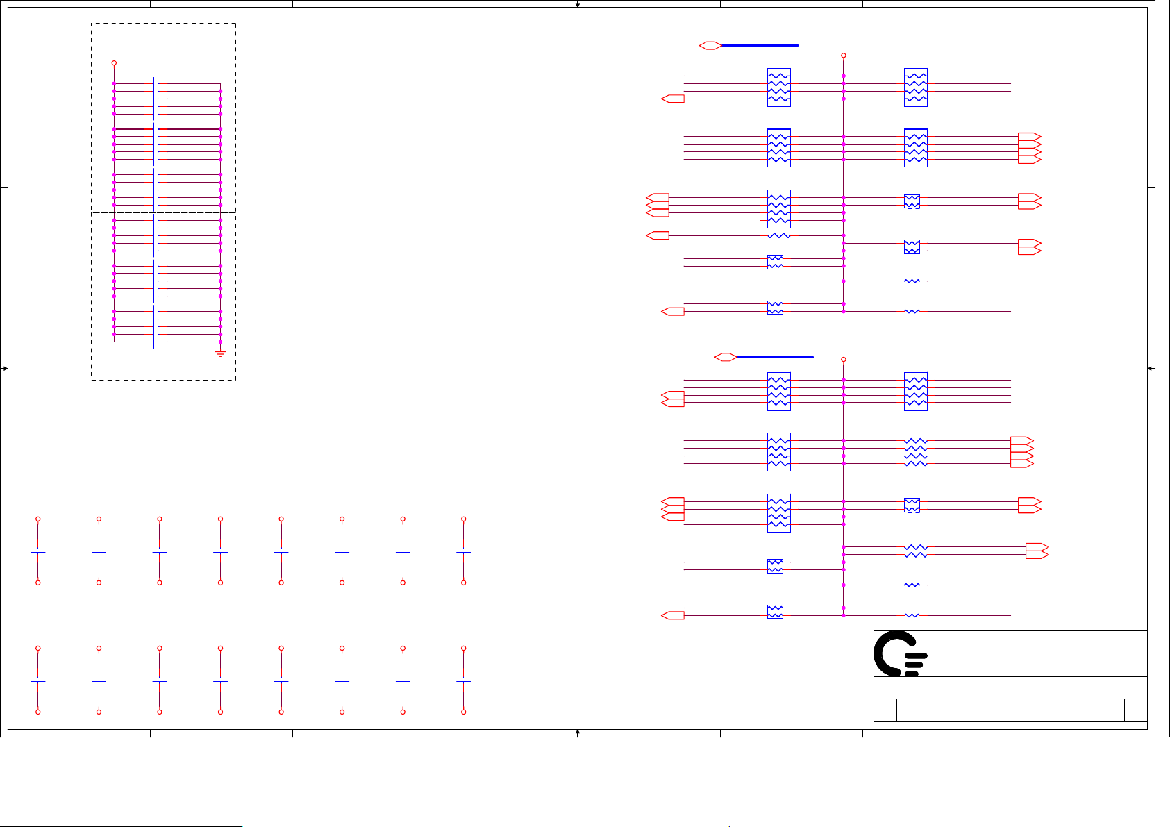
1
Note:
please close to DIMMA
+0.9V_DDR_VTT
C253 0.1U_10VC253 0.1U_10V
1 2
C256 0.1U_10VC256 0.1U_10V
1 2
C260 0.1U_10VC260 0.1U_10V
A A
B B
Note:
please close to DIMMB
Layout Note:
Place one cap close to every 2 pullup
resistors terminated to +0.9V_DDR_VTT
C C
1 2
C366 0.1U_10VC366 0.1U_10V
1 2
C645 0.1U_10VC645 0.1U_10V
1 2
C255 0.1U_10VC255 0.1U_10V
1 2
C257 0.1U_10VC257 0.1U_10V
1 2
C261 0.1U_10VC261 0.1U_10V
1 2
C614 0.1U_10VC614 0.1U_10V
1 2
C359 0.1U_10VC359 0.1U_10V
1 2
C652 0.1U_10VC652 0.1U_10V
1 2
C365 0.1U_10VC365 0.1U_10V
1 2
C357 0.1U_10VC357 0.1U_10V
1 2
C354 0.1U_10VC354 0.1U_10V
1 2
C362 0.1U_10VC362 0.1U_10V
1 2
C363 0.1U_10VC363 0.1U_10V
1 2
C367 0.1U_10VC367 0.1U_10V
1 2
C651 0.1U_10VC651 0.1U_10V
1 2
C646 0.1U_10VC646 0.1U_10V
1 2
C650 0.1U_10VC650 0.1U_10V
1 2
C616 0.1U_10VC616 0.1U_10V
1 2
C648 0.1U_10VC648 0.1U_10V
1 2
C620 0.1U_10VC620 0.1U_10V
1 2
C618 0.1U_10VC618 0.1U_10V
1 2
C346 0.1U_10VC346 0.1U_10V
1 2
C617 0.1U_10VC617 0.1U_10V
1 2
C642 0.1U_10VC642 0.1U_10V
1 2
C612 0.1U_10VC612 0.1U_10V
1 2
C621 0.1U_10VC621 0.1U_10V
1 2
C258 0.1U_10VC258 0.1U_10V
1 2
Note: Reserve stitching function for JDIM1.
+1.8V_SUS
12
+0.9V_DDR_VTT
C252
C252
0.1U
0.1U
16V
16V
+1.8V_SUS
12
C636
C636
0.1U
0.1U
16V
16V
+0.9V_DDR_VTT
+1.8V_SUS
12
C254
C254
0.1U_NC
0.1U_NC
16V
16V
+0.9V_DDR_VTT
Note: Reserve stitching function for JDIM2.
D D
+1.8V_SUS
12
+0.9V_DDR_VTT
C647
C647
0.1U
0.1U
16V
16V
+1.8V_SUS
12
C368
C368
0.1U_NC
0.1U_NC
16V
16V
+0.9V_DDR_VTT
1
+1.8V_SUS
12
C259
C259
0.1U
0.1U
16V
16V
+0.9V_DDR_VTT
2
+1.8V_SUS
12
C364
C364
0.1U_NC
0.1U_NC
16V
16V
+0.9V_DDR_VTT
+1.8V_SUS
12
C637
C637
0.1U_NC
0.1U_NC
16V
16V
+0.9V_DDR_VTT
2
+1.8V_SUS
12
C345
C345
0.1U
0.1U
16V
16V
+0.9V_DDR_VTT
+1.8V_SUS
12
C619
C619
0.1U_NC
0.1U_NC
16V
16V
+0.9V_DDR_VTT
3
+1.8V_SUS
12
C615
C615
0.1U_NC
0.1U_NC
16V
16V
+0.9V_DDR_VTT
+1.8V_SUS
12
C360
C360
0.1U_NC
0.1U_NC
16V
16V
+0.9V_DDR_VTT
3
+1.8V_SUS
12
C613
C613
0.1U_NC
0.1U_NC
16V
16V
+0.9V_DDR_VTT
+1.8V_SUS
12
C649
C649
0.1U
0.1U
16V
16V
+0.9V_DDR_VTT
+1.8V_SUS
12
C262
C262
0.1U
0.1U
16V
16V
+0.9V_DDR_VTT
+1.8V_SUS
12
C622
C622
0.1U
0.1U
16V
16V
+0.9V_DDR_VTT
4
DDR_CKE0_DIMMA9,17
DDR_CS2_DIMMA#9,17 DDR_A_RAS# 9,17
DDR_A_BS29,17
DDR_CKE1_DIMMA9,17
DDR_CKE2_DIMMB9,17
DDR_CS2_DIMMB#9,17
4
5
DDR_A_MA[0..15]9,17
DDR_A_BS09,17
DDR_A_BS19,17
DDR_B_MA[0..15]9,17
DDR_B_BS09,17
DDR_B_WE#9,17
DDR_B_BS29,17
DDR_B_BS19,17
5
DDR_A_MA[0..15]
DDR_A_MA3
DDR_A_MA1
DDR_A_MA10
DDR_A_MA12
DDR_A_MA9
DDR_A_MA8
DDR_A_MA5
R564 47R564 47
DDR_A_MA4
DDR_A_MA2
DDR_A_MA0
DDR_B_MA1
DDR_B_MA10
DDR_B_MA9
DDR_B_MA8
DDR_B_MA5
DDR_B_MA3
DDR_CS2_DIMMB#
DDR_B_MA12
DDR_B_MA4
DDR_B_MA2
DDR_B_MA0
47_1206_8P4R
47_1206_8P4R
47_1206_8P4R
47_1206_8P4R
47_1206_8P4R
47_1206_8P4R
DDR_B_MA[0..15]
47_1206_8P4R
47_1206_8P4R
47_1206_8P4R
47_1206_8P4R
47_1206_8P4R
47_1206_8P4R
RP22
RP22
2
4
6
8
RP23
RP23
2
4
6
8
RP24
RP24
2
4
6
8
1 2
RP19
RP19
1 2
3 4
RP18
RP18
1 2
3 4
RP1
RP1
2
4
6
8
RP2
RP2
2
4
6
8
RP3
RP3
2
4
6
8
RP7
RP7
1 2
3 4
RP6
RP6
1 2
3 4
6
1
3
5
7
1
3
5
7
1
3
5
7
4P2R-47
4P2R-47
4P2R-47
4P2R-47
1
3
5
7
1
3
5
7
1
3
5
7
4P2R-47
4P2R-47
4P2R-47
4P2R-47
6
+0.9V_DDR_VTT
+0.9V_DDR_VTT
7
RP20
RP20
47_1206_8P4R
47_1206_8P4R
1
3
5
7
RP21
RP21
47_1206_8P4R
47_1206_8P4R
1
3
5
7
RP17
RP17
1 2
4P2R-47
4P2R-47
3 4
RP16
RP16
1 2
4P2R-47
4P2R-47
3 4
1 2
R563 47R563 47
1 2
R565 47R565 47
RP4
RP4
47_1206_8P4R
47_1206_8P4R
1
3
5
7
1 2
R270 47R270 47
1 2
R269 47R269 47
1 2
R321 47R321 47
1 2
R323 47R323 47
RP5
RP5
1 2
4P2R-47
4P2R-47
3 4
1 2
R319 47R319 47
1 2
R268 47R268 47
1 2
R322 47R322 47
1 2
R320 47R320 47
Title
Title
Title
DDRII TERMINATION
DDRII TERMINATION
DDRII TERMINATION
Size Document Number Rev
Size Document Number Rev
Size Document Number Rev
MGD 2A
MGD 2A
MGD 2A
Date: Sheet
Date: Sheet
Date: Sheet
DDR_A_MA6
2
DDR_A_MA7
4
DDR_A_MA11
6
DDR_A_MA14
8
2
4
6
8
DDR_CS0_DIMMA#
DDR_A_RAS#
DDR_CS3_DIMMA#
M_ODT0
DDR_A_MA15
DDR_A_MA13
DDR_B_MA6
2
DDR_B_MA7
4
DDR_B_MA11
6
DDR_B_MA14
8
DDR_CS0_DIMMB#
DDR_B_RAS#
DDR_CS3_DIMMB#
M_ODT3
DDR_B_MA15
DDR_B_MA13
QUANTA
QUANTA
QUANTA
COMPUTER
COMPUTER
COMPUTER
7
8
DDR_A_WE# 9,17
DDR_A_CAS# 9,17
DDR_CS1_DIMMA# 9,17
M_ODT1 9,17
DDR_CS0_DIMMA# 9,17
DDR_CS3_DIMMA# 9,17
M_ODT0 9,17
DDR_B_CAS# 9,17
DDR_CS1_DIMMB# 9,17
M_ODT2 9,17
DDR_CKE3_DIMMB 9,17
DDR_CS0_DIMMB# 9,17
DDR_B_RAS# 9,17
DDR_CS3_DIMMB# 9,17
M_ODT3 9,17
18 89Thursday, March 01, 2007
18 89Thursday, March 01, 2007
18 89Thursday, March 01, 2007
of
of
of
8
Page 19
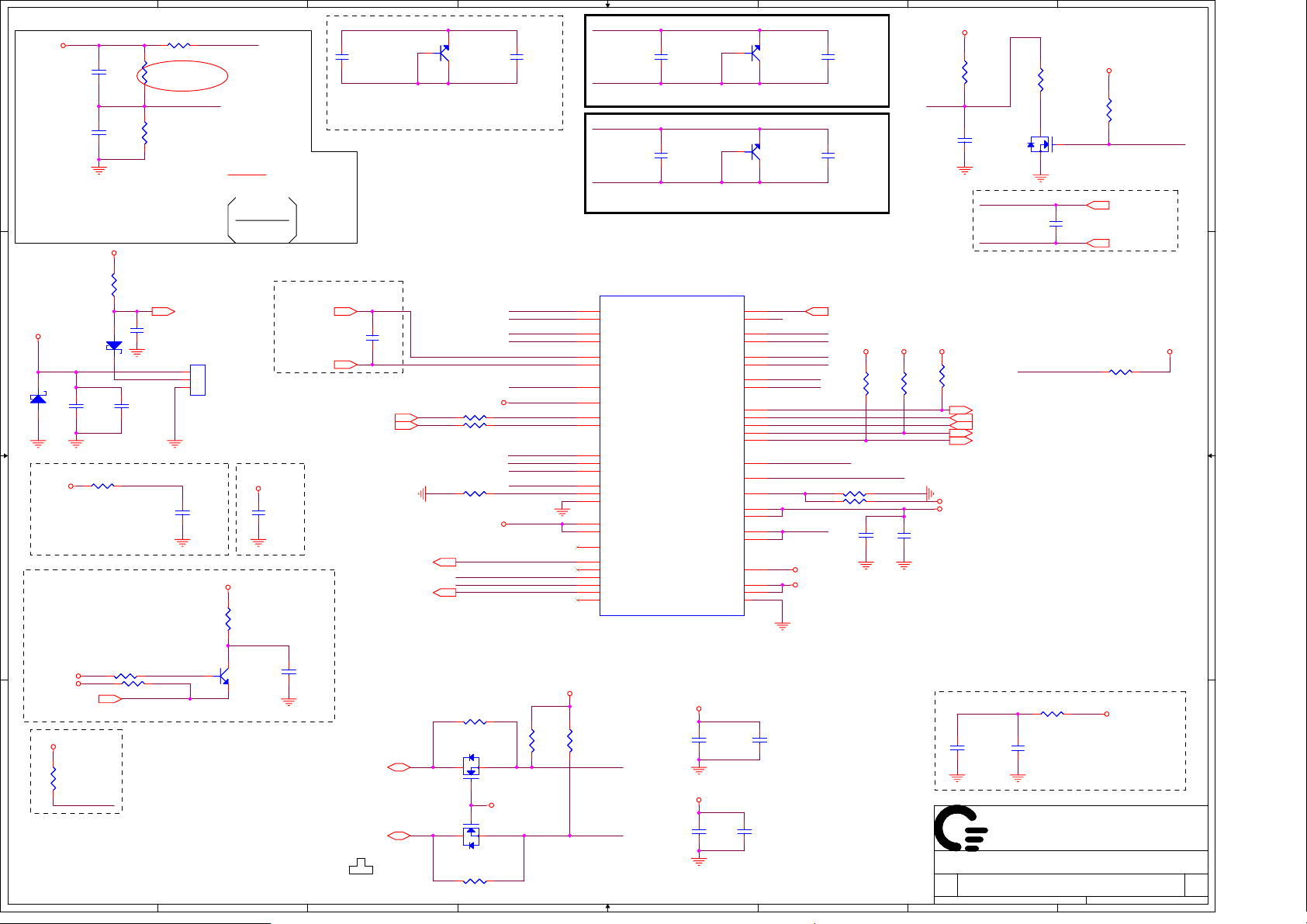
1
R167 8.2KR167 8.2K
R521
R521
10K
10K
1 2
12
+FAN1_VOUT
FAN1_TACH_FB
12
C135
C135
22U_6.3V_NC
22U_6.3V_NC
0805
0805
+3VSUS_THRM
1 2
1 2
R172
R172
71.5K
71.5K
1%
1%
Rc
THERM_VSET
R165
R165
40.2K
40.2K
1%
1%
Rd
VSET =
FAN1_TACH 39
C590
C590
100P_50V_NC
100P_50V_NC
THERM_B1
VSET=
12
+3.3V_SUS
A A
Note:
VSET = (Tp-70)/21, where
Tp = 70 to 101 degrees C.
Tp set at 95 degrees C.
Guardian temp tolerance =
+-3 degrees C.
+FAN1_VOUT
B B
SDMK0340L-7-F_NC
SDMK0340L-7-F_NC
+3.3V_SUS
C C
+1.8V_SUS
+1.8V_SUS
H_THERMTRIP#10
+3.3V_SUS
D D
12
C193
C193
0.1U_16V
0.1U_16V
12
C605
C605
0.1U_16V
0.1U_16V
+3.3V_RUN
D26
D26
SDMK0340L-7-F
SDMK0340L-7-F
D11
D11
12
C134
C134
22U_6.3V
22U_6.3V
0805
0805
R131
R131
1 2
49.9_F_0603
49.9_F_0603
C190 needs to be placed
near Guardian IC.
R182 2.2KR182 2.2K
1 2
R183 300R183 300
12
R174
R174
8.2K
8.2K
THERMATRIP2#
1
THERMATRIP3#
A00-09
Rc+Rd
J6
J6
1
2
3
MLX_53398-0371
MLX_53398-0371
C167
C167
0.1U_16V
0.1U_16V
+3.3V_SUS
12
2
1 3
2
Rd
Tp-70
21
+RTC_CELL
12
C176
C176
0.1U
0.1U
0603
0603
16
16
X7R
X7R
R168
R168
8.2K
8.2K
THERMATRIP1#
Q20
Q20
MMST3904
MMST3904
2
x 3.3V
H_THERMDA10
H_THERMDC10
12
C190
C190
0.1U_16V
0.1U_16V
3
REM_DIODE2_N
C175
C175
220P
220P
50
50
REM_DIODE2_P
Put C175 close to Guardian.
Put C541 close to Diode
13
2
Place under CPU
C188
C188
220P
220P
50
50
SUSPWROK39,43
SB_PWRGD#43
THRM_SMBDAT39,46
THRM_SMBCLK39,46
GDS
2N7002W-7-F
MDC_RST_DIS#34
AUDIO_AVDD_ON28
3
1
2
3
R140 1KR140 1K
R177 1KR177 1K
R133 1KR133 1K
+FAN1_VOUT
R558 0_NCR558 0_NC
R556 0_NCR556 0_NC
Q62
Q62
MMST3904
MMST3904
+RTC_CELL
1 2
1 2
1 2
Q67
Q67
2N7002W-7-F
2N7002W-7-F
3 1
2
2
3 1
2N7002W-7-F
2N7002W-7-F
Q66
Q66
C541
C541
220P
220P
50
50
EMC_SMBDAT
EMC_SMBCLK
REM_DIODE2_P
REM_DIODE2_N
H_THERMDA
H_THERMDC
+3VSUS_THRM
THERMATRIP1#
THERMATRIP2#
THERMATRIP3#
THERM_VSET
+FAN1_VOUT
5V_CAL_SIO1#
5V_CAL_SIO2#
12
+3.3V_SUS
12
4
1 2
4
R559
R559
2.2K
2.2K
+3.3V_SUS
R557
R557
1 2
REM_DIODE3_N
REM_DIODE3_P
REM_DIODE4_N
REM_DIODE4_P
U8
U8
11
SMDATA
12
SMBCLK
38
DP1
37
DN1
41
DP2
40
DN2
35
3V_SUS
21
RTC_PWR3V
23
VSUS_PWRGD
16
3V_PWROK#
17
THERMTRIP1#
18
THERMTRIP2#
19
THERMTRIP3#
42
VSET
26
XEN
34
VSS
7
FAN_OUT_1
8
FAN_OUT_2
39
FAN_DAC1
10
GPIO1
13
GPIO2
14
GPIO3
15
GPIO4
22
GPIO5
36
GPIO6/FAN_DAC2
EMC4001
EMC4001
2.2K
2.2K
EMC_SMBDAT
EMC_SMBCLK
5
Place Q68 and C609 near the Bottom SODIMM
13
Q68
VCP1
VCP2
DP3
DN3
DP4
DN4
DP5
DN5
2
2
12
Q68
MMST3904
MMST3904
13
Q63
Q63
MMST3904
MMST3904
43
VCP2
46
REM_DIODE3_P
45
REM_DIODE3_N
44
REM_DIODE4_P
48
REM_DIODE4_N
47
NB_THERMDA
2
NB_THERMDC
1
20
3
4
25
24
2.5V_RUN_ON
27
NC_2.5V_RUN_PWRGD
33
LDO_SET
28
32
31
30
29
9
5
6
49
12
C213
C213
10U_10V_0805
10U_10V_0805
R538 1KR538 1K
R124 31.6K_NC
R124 31.6K_NC
+3V_LDOIN
+3.3V_RUN
+5V_RUN
Layout Note:
Place those capacitors
close to EMC4001.
C214
C214
10U_10V_0805
10U_10V_0805
C610
C610
220P
220P
50
50
Place C610, C609 < 100mils
from the Guardian pins
C196
C196
220P
220P
50
50
Place Q63 and C579 in between the
CPU, North Bridge and South Bridge
EMC 4001
EMC 4001
QFN PIN48
QFN PIN48
ATF_INT#
POWER_SW#
ACAVAIL_CLR
THERMTRIP_SIO
SYS_SHDN#
LDO_SHDN#/ADDR
LDO_POK
LDO_SET
LDO_OUT2
LDO_OUT1
LDO_IN2
LDO_IN1
VDD_3V
VDD_5V_1
VDD_5V_2
GNDPAD
+3.3V_RUN
12
C204
C204
0.1U_16V
0.1U_16V
+5V_RUN
12
C203
C203
0.1U_16V
0.1U_16V
5
6
C609
C609
220P_NC
220P_NC
50
50
C579
C579
220P_NC
220P_NC
50
50
PWR_MON 50
1 2
1 2
6
12
R138
R138
47K_NC
47K_NC
1%
1%
C164
C164
0.1U
0.1U
16V
16V
X5R
X5R
7
+5V_SUS
R256
R256
2.21K
2.21K
1%
1%
0603
0603
VCP2
12
C265
C265
2200P_50V
2200P_50V
NB_THERMDA
NB_THERMDC
+3.3V_SUS+RTC_CELL +3.3V_ALW
R150
R150
R134
R134
10K
10K
10K
10K
1 2
1 2
12
C131
C131
10U
10U
X5R
X5R
6.3
6.3
0603
0603
ATF_INT# 38
POWER_SW# 40
ACAV_IN 39,46,51
THERMTRIP_SIO
THERM_STP# 47
+2.5V_RUN
+2.5V_RUN
+3V_LDOIN
12
C165
C165
0.1U_16V
0.1U_16V
QUANTA
QUANTA
QUANTA
COMPUTER
COMPUTER
Title
Title
Title
Size Document Number Rev
Size Document Number Rev
Size Document Number Rev
Date: Sheet
Date: Sheet
Date: Sheet
COMPUTER
FAN & THERMAL
FAN & THERMAL
FAN & THERMAL
MGD 3A
MGD 3A
MGD 3A
7
This unused thermistor circuit is
located under the top
memory module
+3.3V_SUS
R260
R260
NTC_10K
NTC_10K
0603
0603
31
2N7002W-7-F
2N7002W-7-F
2.5V_RUN_ON
R123 0.27_1210R123 0.27_1210
1 2
C604
C604
10U
10U
10
10
0805
0805
Q25
Q25
2
C202
C202
220P
220P
50
50
R243
R243
10K
10K
1 2
NB_THERMDA 14
NB_THERMDC 14
R132 7.5KR132 7.5K
+3.3V_RUN
8
5V_CAL_SIO1#
of
of
of
19 89Thursday, March 01, 2007
19 89Thursday, March 01, 2007
19 89Thursday, March 01, 2007
8
+3.3V_SUS
Page 20
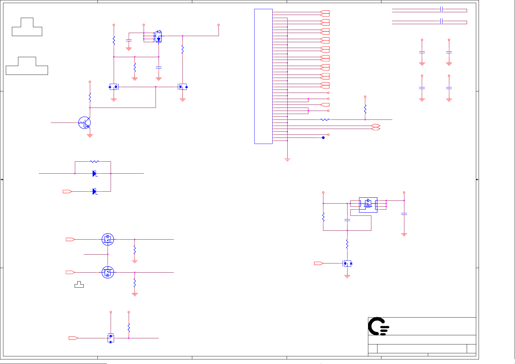
5
Symbol:
2N7002W-7-F
D(3)
G(2)
S(1)
Symbol:
D D
DTC124EUA
+15V_ALW +LCDVDD+3.3V_RUN
R464
R464
100K
100K
1 2
LCDVCC_ON
OUT(3)
IN(2)
C C
B B
GND(1)
+15V_ALW
R463
R463
100K
100K
1 2
EN_LCDVDD_2
EN_LCDVDD_1 EN_LCDVDD_2
LCDVCC_TST_EN39
EN_LCDVDD14
BIA_PWM14
2
Q52
Q52
DTC124EUAT-106
DTC124EUAT-106
1 3
R466 0_NCR466 0_NC
D25
D25
SDMK0340L-7-F
SDMK0340L-7-F
D24
D24
SDMK0340L-7-F
SDMK0340L-7-F
3
NB_PWRGD_5V
3
D
GS
231
BSS138_NL
WI102034
31
Q59
Q59
BSS138_NL
BSS138_NL
2
2
Q60
Q60
BSS138_NL_NC
BSS138_NL_NC
Q55
Q55
2N7002W-7-F
2N7002W-7-F
1
1
2
12
C489
C489
0.1U_16V
0.1U_16V
R447
R447
100K_NC
100K_NC
1 2
R4702KR470
2K
1 2
R462
R462
2K_NC
2K_NC
1 2
4
6
5
2
1
EN_LCDVDD_1
BACKLITEON
Q57
Q57
SI3456DV-T1-E3
SI3456DV-T1-E3
4
3
C480
C480
0.1U_50V_0603
0.1U_50V_0603
1 2
2
R440
R440
470
470
1 2
31
Q54
Q54
2N7002W-7-F
2N7002W-7-F
3
J4
J4
44
44
43
43
42
42
41
41
40
40
39
39
38
38
37
37
36
36
35
35
34
34
33
33
32
32
31
31
30
30
29
29
28
28
27
27
26
26
25
25
24
24
23
23
22
22
21
21
20
20
19
19
18
18
17
17
16
16
15
15
14
14
13
13
12
12
11
11
10
10
9
9
8
8
7
7
6
6
5
5
4
4
3
3
2
2
1
1
JAE_FI-TD44SB-E-R750
JAE_FI-TD44SB-E-R750
LCD_BCLKLCD_BCLK+
LCD_B2LCD_B2+
LCD_B1LCD_B1+
LCD_B0LCD_B0+
LCD_ACLKLCD_ACLK+
LCD_A2LCD_A2+
LCD_A1LCD_A1+
LCD_A0LCD_A0+
LCD_DDCCLK
LCD_DDCDAT
BACKLITEON_R
LAMP_D_STAT#
RUN_ON33,39,42,43
2
LCD_BCLK- 14
LCD_BCLK+ 14
LCD_B2- 14
LCD_B2+ 14
LCD_B1- 14
LCD_B1+ 14
LCD_B0- 14
LCD_B0+ 14
LCD_ACLK- 14
LCD_ACLK+ 14
LCD_A2- 14
LCD_A2+ 14
LCD_A1- 14
LCD_A1+ 14
LCD_A0- 14
LCD_A0+ 14
LCD_DDCCLK 14
LCD_DDCDAT 14
R468
R468
1 2
T21
T21
+3.3V_RUN
+LCDVDD
LCD_TST 38
+INV_PWR_SRC
0_NC
0_NC
+5V_ALW
PAD
PAD
+3.3V_RUN
Design current: 560mA
Max current: 800mA
+PWR_SRC
40mil
R448
R448
200K
200K
2
C475
C475
1000P_50V
1000P_50V
1 2
R439
R439
100K
100K
1 2
31
Q53
Q53
2N7002W-7-F
2N7002W-7-F
FDS4435BZ
FDS4435BZ
Q56
Q56
1
2
3
R467
R467
10K_NC
10K_NC
1 2
BACKLITEON
LCD_SMBCLK 39
LCD_SMBDAT 39
+INV_PWR_SRC
40mil
8
7
6
54
1
LCD_BCLK-
C484 3.3P_NC
C484 3.3P_NC
LCD_BCLK+
LCD_ACLK-
C476 3.3P_NC
C476 3.3P_NC
LCD_ACLK+
+LCDVDD
12
C77
C77
0.1U_16V
0.1U_16V
+5V_ALW
12
C79
C79
0.1U_16V
0.1U_16V
Adress : A9H --Contrast
AAH --Backlight
12
C474
C474
0.1U_50V_0603
0.1U_50V_0603
1 2
1 2
+3.3V_RUN
+INV_PWR_SRC
50 COG
50 COG
50 COG
50 COG
12
C76
C76
0.1U_16V
0.1U_16V
12
C78
C78
0.1U_50V_0603
0.1U_50V_0603
+5V_RUN
A A
NB_PWRGD14,39
5
+3.3V_SUS
2
31
2N7002W-7-F
2N7002W-7-F
Q58
Q58
R469
R469
10K
10K
1 2
NB_PWRGD_5V
4
QUANTA
QUANTA
QUANTA
COMPUTER
COMPUTER
Title
Title
Title
Size Document Number Rev
Size Document Number Rev
Size Document Number Rev
Date: Sheet
Date: Sheet
3
2
Date: Sheet
COMPUTER
LCD CONN & CK-SSCD
LCD CONN & CK-SSCD
LCD CONN & CK-SSCD
MGD 2A
MGD 2A
MGD 2A
1
of
of
of
20 89Thursday, March 01, 2007
20 89Thursday, March 01, 2007
20 89Thursday, March 01, 2007
Page 21
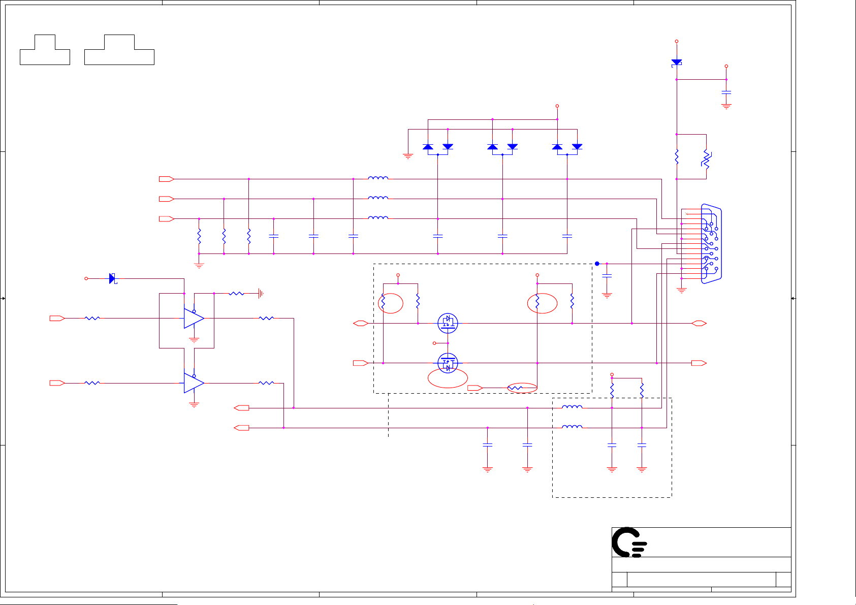
Symbol:
BSS138_NL
D(3)
G(2)
S(1)
A
N(1)
Symbol:
DA204U
P(3)N
P(2)
B
C
D
+5V_RUN
21
D21
D21
SDM10U45-7
SDM10U45-7
E
+CRT_VCC
4 4
+3.3V_RUN
2
1
D20
D20
DA204U_NC
DA204U_NC
R15
R15
4.7K
4.7K
1 2
+3.3V_RUN
1
1
3
12
C6
C6
10P_50V_NC
10P_50V_NC
Q4
Q4
BSS138_NL
BSS138_NL
2
2
Q2
Q2
BSS138_NL
BSS138_NL
DVI_SCLK14,36
3
3
A00-10
L1
VGA_RED14,36
VGA_GRN14,36
3 3
D22 SDM10U45-7D22 SDM10U45-7
+5V_RUN
CRT_HSYNC14
2 2
CRT_VSYNC14
R382 39R382 39
R392 39R392 39
2 1
1 2
1 2
VGA_BLU14,36
CRT_HSYNC_R
CRT_VSYNC_R
+5V_RUN_SYNC
1 2
15
U26
U26
2 4
3
74AHCT1G125GW
74AHCT1G125GW
15
U27
U27
2 4
3
74AHCT1G125GW
74AHCT1G125GW
R7
150_FR7150_F
1 2
R383 1KR383 1K
VGAHSYNC
VGAVSYNC
HSYNC36
VSYNC36
R6
150_FR6150_F
R10
R10
150_F
150_F
1 2
12
R380 0R380 0
1 2
R388 0R388 0
1 2
12
C7
C7
22P_50V_NC
22P_50V_NC
12
C5
C5
22P_50V_NC
22P_50V_NC
G_CLK_DDC214 DOCK_CLK_DDC2 36
L1
BLM18BB600SN1D 0603
BLM18BB600SN1D 0603
L2
L2
BLM18BB600SN1D 0603
BLM18BB600SN1D 0603
L3
L3
BLM18BB600SN1D 0603
BLM18BB600SN1D 0603
12
C9
C9
22P_50V_NC
22P_50V_NC
+3.3V_RUN
R11
R11
4.7K
4.7K
1 2
A00-10 A00-10
RS690 Revision A11 bring-up and qualification has
identified an issue with the DAC_SCL pin
2
1
D18
D18
DA204U_NC
DA204U_NC
3
12
C4
C4
10P_50V_NC
10P_50V_NC
A00-10
R13 0_NCR13 0_NC
12
C424
C424
10P_50V
10P_50V
+5V_RUN_SYNC
R8
6.8KR86.8K
1 2
12
C418
C418
10P_50V
10P_50V
2
1
D19
D19
DA204U_NC
DA204U_NC
3
12
C10
C10
10P_50V_NC
10P_50V_NC
T74T74
R14
R14
6.8K
6.8K
1 2
L43
L43
1 2
BLM18AG121SN1D_0603
BLM18AG121SN1D_0603
L44
L44
1 2
BLM18AG121SN1D_0603
BLM18AG121SN1D_0603
RED
GREEN
BLUE
M_ID2#
12
C8
C8
0.1U_16V_0402
0.1U_16V_0402
+5V_RUN_SYNC
12
R384
R384
1K_NC
1K_NC
HSYNC_L
VSYNC_L
C410
C410
10P_NC
10P_NC
50
50
12
R386
R386
1K_NC
1K_NC
C411
C411
10P_NC
10P_NC
50
50
12
R391
R391
0_1206
0_1206
+CRT_VCC_R
6
11
1
7
12
2
8
13
3
9
14
4
10
15
5
FOX_DS01A91-MD221-7F
FOX_DS01A91-MD221-7F
12
JVGA1
JVGA1
DOCK_DAT_DDC2 36G_DAT_DDC214
C422
C422
0.01U_16V
0.01U_16V
1 2
48
48
0.12
0.12
FUSE 0.12A_NC
FUSE 0.12A_NC
FS1
FS1
For A11:Pop R13 and Nonpop Q2,R11,R8
For A12:Pop Q2,R11,R8 and Nonpop R13
Place near JVGA1 connector <
200 mil
1 1
QUANTA
QUANTA
QUANTA
COMPUTER
COMPUTER
Title
Title
Title
Size Document Number Rev
Size Document Number Rev
Size Document Number Rev
Date: Sheet
Date: Sheet
A
B
C
D
Date: Sheet
COMPUTER
CRT CONN
CRT CONN
CRT CONN
MGD 3A
MGD 3A
MGD 3A
E
of
of
of
21 89Thursday, March 01, 2007
21 89Thursday, March 01, 2007
21 89Thursday, March 01, 2007
Page 22
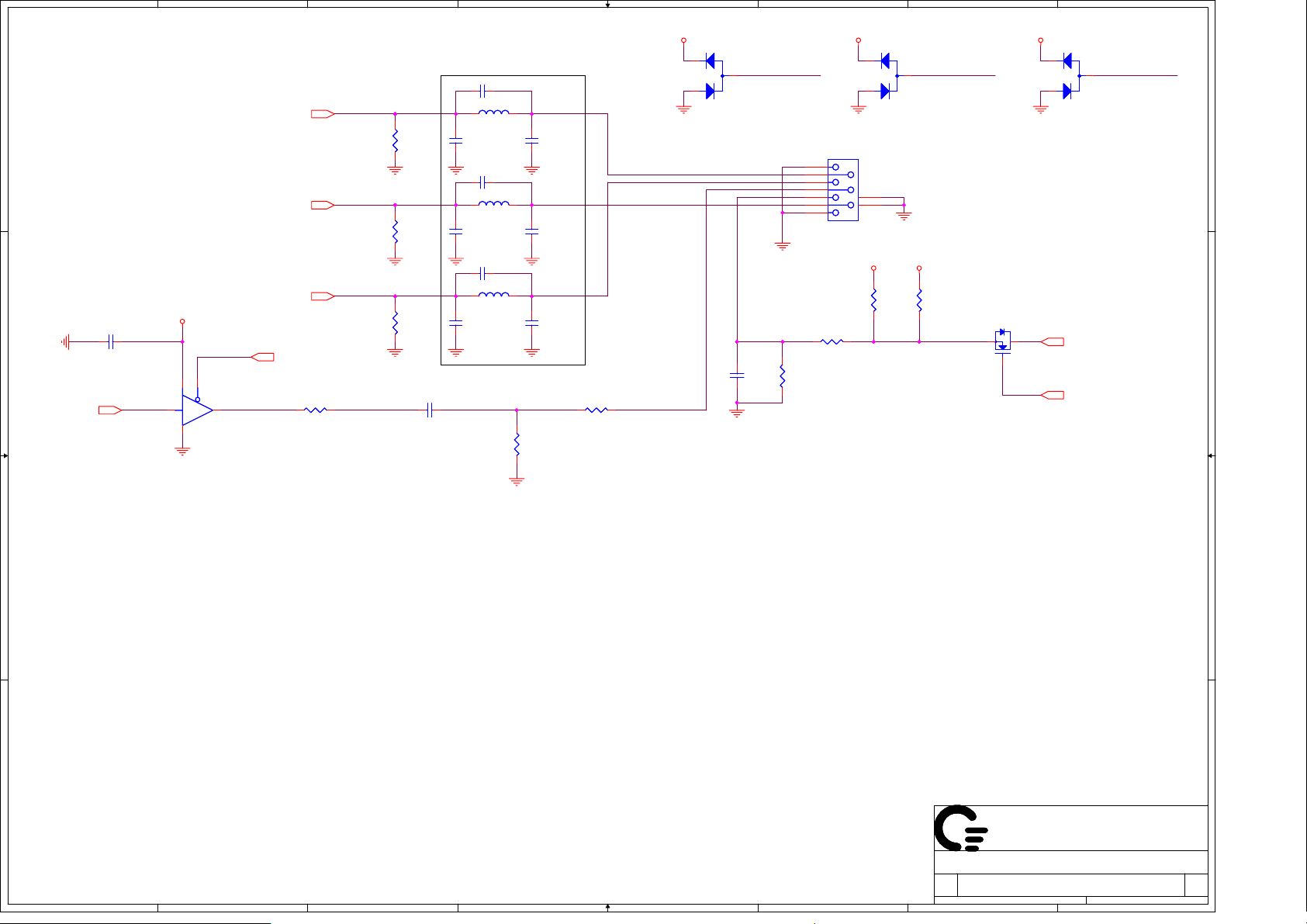
1
2
3
4
5
6
7
8
+3.3V_RUN
Place All of those
Inductors Caps close
to JTV1 <200 mils
C414 22P_50V_NCC414 22P_50V_NC
L47 0.47uH 0603
L47 0.47uH 0603
1 2
%
%
±20
±20
12
C425
C425
47P
47P
50
50
NPO
NPO
C417 22P_50V_NCC417 22P_50V_NC
L45 0.47uH 0603
L45 0.47uH 0603
1 2
%
%
±20
±20
12
C428
C428
47P
47P
50
50
NPO
NPO
C419 22P_50V_NCC419 22P_50V_NC
L46 0.47uH 0603
L46 0.47uH 0603
1 2
%
%
±20
±20
12
C429
C429
47P
47P
50
50
NPO
NPO
12
35m
35m
35m
35m
35m
35m
A
A
A
12
12
C415
C415
47P
47P
50
50
NPO
NPO
12
C413
C413
47P
47P
50
50
NPO
NPO
12
C420
C420
47P
47P
50
50
NPO
NPO
R387
R387
110_0603_NC
110_0603_NC
Add R387 pre
ref schematic.
SVIDEO_C
SVIDEO_CVBS
SVIDEO_Y
1 2
R381 0_0805_NCR381 0_0805_NC
1 2
TV_C
TV_Y
TV_CVBS
12
R395
R395
150
150
1%
1%
12
R393
R393
150
150
1%
1%
0402
0402
12
R394
R394
150
150
1%
1%
C409 0.01U_25V_NCC409 0.01U_25V_NC
A A
+5V_RUN
12
C402 0.1U_NC
B B
AUD_SPDIF_OUT28,36
C402 0.1U_NC
10 0402
10 0402
1
53
2 4
U24
U24
74AHCT1G125GW_NC
74AHCT1G125GW_NC
TV_C14,36
TV_Y14,36
TV_CVBS14,36
AUD_SPDIF_SHDN 28,38
SP_DIF SP_DIFB SP_DIFC SP_DIF_D
R377 220_0603_NCR377 220_0603_NC
1
2
D3
D3
DA204U_NC
DA204U_NC
SVIDEO_C SVIDEO_Y SVIDEO_CVBS
3
SP_DIF_E
12
C433
C433
300P_NC
300P_NC
Populate R390 & De-populate R389
when component VIDEO is enable.
R390 0_0805R390 0_0805
R389
R389
0_0805_NC
0_0805_NC
1 2
1 2
1
2
JTV1
JTV1
3
6
7
5
2
8
4
9
1
MH1177L-BG5N-7F
MH1177L-BG5N-7F
+3.3V_RUN +1.8V_RUN
D1
D1
DA204U_NC
DA204U_NC
12
R396
R396
47K_NC
47K_NC
0603
0603
3
12
R416
R416
10K
10K
+3.3V_RUN+3.3V_RUN
Q51
Q51
2N7002W-7-F_NC
2N7002W-7-F_NC
31
Vgs = 20
Vgs = 20
Vds = 60
Vds = 60
2
Current = 115m
Current = 115m
Type = Single N
Type = Single N
1
3
2
D2
D2
DA204U_NC
DA204U_NC
DFT_GPIO5 14
PLTRST_SYS# 14,30,35,43,49
C C
D D
QUANTA
QUANTA
QUANTA
COMPUTER
COMPUTER
Title
Title
Title
Size Document Number Rev
Size Document Number Rev
Size Document Number Rev
Date: Sheet
Date: Sheet
1
2
3
4
5
6
Date: Sheet
COMPUTER
S-Video
MGD 3A
MGD 3A
MGD 3A
7
of
of
of
22 89Thursday, March 01, 2007
22 89Thursday, March 01, 2007
22 89Thursday, March 01, 2007
8
Page 23
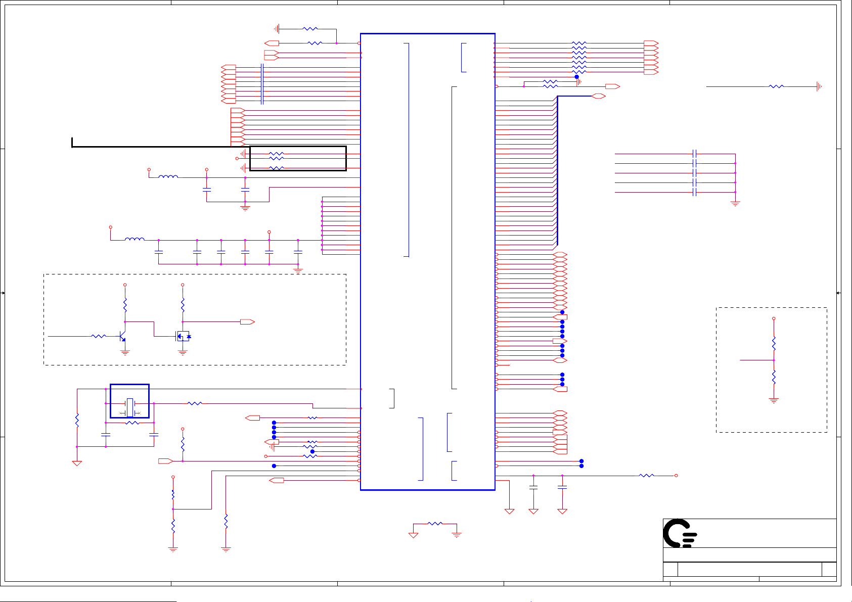
5
4
3
2
1
R631 8.2KR631 8.2K
PLTRST#27,38,39,43
CLK_PCIE_SB7
CLK_PCIE_SB#7
ALINK_NBRX_SBTX_P013
ALINK_NBRX_SBTX_N013
D D
Place R346,R348,R344
< 100mils from pins E27,E28,E29
C C
CPU_PWRGD
B B
A A
+1.2V_RUN
L73
L73
BLM21PG221SN1D_0805
BLM21PG221SN1D_0805
+5V_ALW +3.3V_ALW
R370
R370
10K
10K
R369 1KR369 1K
ATi Recommend
Vendor: NSK
Part Number: NXG 32.768KAE12FUD 16 PPM.
R345
R345
20M
20M
RTC_GNDRTC_GNDRTC_GND
H_DPSLP# should be put down ,
reserve R592 for verifing
5
Q43
Q43
2
MMBT3904
MMBT3904
1 3
Y2
Y2
32.768KHZ
32.768KHZ
R342 20MR342 20M
C376
C376
18P_50V
18P_50V
ALLOW_LDTSTOP14
14
23
ALINK_NBRX_SBTX_P113
ALINK_NBRX_SBTX_N113
ALINK_NBRX_SBTX_P213
ALINK_NBRX_SBTX_N213
ALINK_NBRX_SBTX_P313
ALINK_NBRX_SBTX_N313
ALINK_NBTX_C_SBRX_P013
ALINK_NBTX_C_SBRX_N013
ALINK_NBTX_C_SBRX_P113
ALINK_NBTX_C_SBRX_N113
ALINK_NBTX_C_SBRX_P213
ALINK_NBTX_C_SBRX_N213
ALINK_NBTX_C_SBRX_P313
ALINK_NBTX_C_SBRX_N313
+1.2V_RUN
L74
L74
BLM21PG221SN1D_0805
BLM21PG221SN1D_0805
PCIE Power
C684
C684
22U
22U
6.3
6.3
0805
0805
X5R
X5R
2
R341 0R341 0
+1.8V_RUN
C375
C375
18P_50V
18P_50V
+3.3V_RUN
+1.2V_PCIE_VDDR
+1.2V_PCIE_PVDD
12
C699
C699
10U
10U
4
4
±20
±20
0603
0603
X5R
X5R
50mil Width
C686
C686
1U
1U
6.3
6.3
%
%
±10
±10
X5R
X5R
R367
R367
10K
10K
CPU_PWRGD_Q
31
Q44
Q44
2N7002W-7-F
2N7002W-7-F
Place the translation circuit for CPU_PWRGD close to the
SB600 to minimize stubbs when the circuit is No Stuff.
CPU_PWRGD10
R6251KR625
1K
R591
R591
10K
10K
H_DPSLP#
R592
R592
100K_NC
100K_NC
C391 0.1UC391 0.1U
C389 0.1UC389 0.1U
C387 0.1UC387 0.1U
C385 0.1UC385 0.1U
C380 0.1UC380 0.1U
C383 0.1UC383 0.1U
C379 0.1UC379 0.1U
C377 0.1UC377 0.1U
R346 562 1%R346 562 1%
R348 2.05K 1%R348 2.05K 1%
R344 0R344 0
C697
C697
1U
1U
6.3
C683
C683
1U
1U
6.3
6.3
±10
±10
X5R
X5R
R617
R617
100K_NC
100K_NC
%
%
LDT_STOP#10,14
+1.8V_RUN
6.3
X5R
X5R
%
%
±10
±10
+1.2V_PCIE_VDDR
C690
C690
1U
1U
6.3
6.3
%
%
±10
±10
X5R
X5R
CPU_PWRGD_Q 39
T157T157
T170T170
T158T158
T165T165
LDT_RST#10
4
%
%
R371 33R371 33
ALINK_NBRX_C_SBTX_P0
ALINK_NBRX_C_SBTX_N0
ALINK_NBRX_C_SBTX_P1
ALINK_NBRX_C_SBTX_N1
ALINK_NBRX_C_SBTX_P2
ALINK_NBRX_C_SBTX_N2
ALINK_NBRX_C_SBTX_P3
ALINK_NBRX_C_SBTX_N3
20mil Width
C680
C680
0.1U_10V
0.1U_10V
CPU_PWRGD
R361 0R361 0
R623 300R623 300
R358 10K_NCR358 10K_NC
PCIE_CALRP
PCIE_CALRN
PCIE_CALI
C694
C694
0.1U_10V
0.1U_10V
R364 0R364 0
T162T162
32K_X1
32K_X2
U23A
U23A
AG10
A_RST#
J24
PCIE_RCLKP
J25
PCIE_RCLKN
P29
PCIE_TX0P
P28
PCIE_TX0N
M29
PCIE_TX1P
M28
PCIE_TX1N
K29
PCIE_TX2P
K28
PCIE_TX2N
H29
PCIE_TX3P
H28
PCIE_TX3N
T25
PCIE_RX0P
T26
PCIE_RX0N
T22
PCIE_RX1P
T23
PCIE_RX1N
M25
PCIE_RX2P
M26
PCIE_RX2N
M22
PCIE_RX3P
M23
PCIE_RX3N
E29
PCIE_CALRP
E28
PCIE_CALRN
E27
PCIE_CALI
U29
PCIE_PVDD
U28
PCIE_PVSS
F27
PCIE_VDDR_1
F28
PCIE_VDDR_2
F29
PCIE_VDDR_3
G26
PCIE_VDDR_4
G27
PCIE_VDDR_5
G28
PCIE_VDDR_6
G29
PCIE_VDDR_7
J27
PCIE_VDDR_8
J29
PCIE_VDDR_9
L25
PCIE_VDDR_10
L26
PCIE_VDDR_11
L29
PCIE_VDDR_12
N29
PCIE_VDDR_13
D2
X1
C1
X2
AC26
CPU_PG/LDT_PG
W26
INTR/LINT0
W24
NMI/LINT1
W25
INIT#
AA24
SMI#
AA23
SLP#/LDT_STP#
AA22
IGNNE#/SIC
AA26
A20M#/SID
Y27
FERR#
AA25
STPCLK#/ALLOW_LDTSTP
AH9
CPU_STP#/DPSLP_3V#
B24
DPSLP_OD#/GPIO37
W23
DPRSLPVR
AC25
LDT_RST#/DPRSTP#/PROCHOT#
SB600 A13
SB600 A13
SB600 SB 27x27mm
SB600 SB 27x27mm
Part 1 of 4
Part 1 of 4
SPDIF_OUT/PCICLK7/GPIO41
AD0/ROMA18
AD1/ROMA17
PCI CLKS
PCI CLKS
AD2/ROMA16
AD3/ROMA15
AD4/ROMA14
AD5/ROMA13
AD6/ROMA12
AD7/ROMA11
AD10/ROMA7
AD11/ROMA6
AD12/ROMA5
AD13/ROMA4
AD14/ROMA3
AD15/ROMA2
AD16/ROMD0
AD17/ROMD1
AD18/ROMD2
AD19/ROMD3
AD20/ROMD4
AD21/ROMD5
AD22/ROMD6
AD23/ROMD7
CBE0#/ROMA10
CBE1#/ROMA1
CBE2#/ROMWE#
PCI INTERFACE
PCI INTERFACE
DEVSEL#/ROMA0
TRDY#/ROMOE#
PCI EXPRESS INTERFACE
PCI EXPRESS INTERFACE
XTAL
XTAL
CPU
CPU
R343 0R343 0
RTC_GND
3
PAR/ROMA19
REQ3#/GPIO70
REQ4#/GPIO71
GNT3#/GPIO72
GNT4#/GPIO73
INTE#/GPIO33
INTF#/GPIO34
INTG#/GPIO35
INTH#/GPIO36
LPC
LPC
LDRQ1#/GNT5#/GPIO68
BMREQ#/REQ5#/GPIO65
RTC_IRQ#/GPIO69
RTC
RTC
PCICLK0
PCICLK1
PCICLK2
PCICLK3
PCICLK4
PCICLK5
PCICLK6
PCIRST#
AD8/ROMA9
AD9/ROMA8
AD24
AD25
AD26
AD27
AD28
AD29
AD30
AD31
CBE3#
FRAME#
IRDY#
STOP#
PERR#
SERR#
REQ0#
REQ1#
REQ2#
GNT0#
GNT1#
GNT2#
CLKRUN#
LOCK#
LAD0
LAD1
LAD2
LAD3
LFRAME#
LDRQ0#
SERIRQ
RTCCLK
VBAT
RTC_GND
Rev.A21
U2
T2
U1
V2
W3
U3
V1
T1
AJ9
W7
Y1
W8
W5
AA5
Y3
AA6
AC5
AA7
AC3
AC7
AJ7
AD4
AB11
AE6
AC9
AA3
AJ4
AB1
AH4
AB2
AJ3
AB3
AH3
AC1
AH2
AC2
AH1
AD2
AG2
AD1
AG1
AB9
AF9
AJ5
AG3
AA2
AH6
AG5
AA1
AF7
Y2
AG8
AC11
AJ8
AE2
AG9
AH8
AH5
AD11
AF2
AH7
AB12
AG4
AG7
AF6
AD3
AF1
AF4
AF3
AG24
AG25
AH24
AH25
AF24
AJ24
AH26
W22
AF23
D3
F5
E1
D1
RTC_GND
PCI_CLK0_R
PCI_CLK1_R
PCI_CLK2_R
PCI_CLK3_R
PCI_CLK4_R
PCI_CLK5_R
PCI_CLK6_R
SB_SPDIF_OUT_R
R372 8.2KR372 8.2K
R373 33R373 33
PCI_AD0
PCI_AD1
PCI_AD2
PCI_AD3
PCI_AD4
PCI_AD5
PCI_AD6
PCI_AD7
PCI_AD8
PCI_AD9
PCI_AD10
PCI_AD11
PCI_AD12
PCI_AD13
PCI_AD14
PCI_AD15
PCI_AD16
PCI_AD17
PCI_AD18
PCI_AD19
PCI_AD20
PCI_AD21
PCI_AD22
PCI_AD23
PCI_AD24
PCI_AD25
PCI_AD26
PCI_AD27
PCI_AD28
PCI_AD29
PCI_AD30
PCI_AD31
PCI_FRAME#
PCI_DEVSEL#
PCI_IRDY#
PCI_TRDY#
PCI_PAR
PCI_STOP#
PCI_PERR#
PCI_SERR#
PCI_REQ0#
PCI_REQ1#
PCI_REQ2#
PCI_REQ3#
PCI_REQ4#
PCI_GNT0#
PCI_GNT1#
PCI_GNT2#
PCI_GNT3#
PCI_GNT4#
CLKRUN#
PCI_PIRQA#
PCI_PIRQB#
PCI_PIRQC#
PCI_PIRQD#
LPC_LAD0
LPC_LAD1
LPC_LAD2
LPC_LAD3
LPC_LFRAME#
LPC_LDRQ0#
LPC_LDRQ1#
BMREQ#
IRQ_SERIRQ
+VBAT_IN
C378
C378
1U
1U
10
10
0603
0603
X6S
X6S
%
%
±10
±10
RTC_GND
R359 22R359 22
R354 22R354 22
R357 22R357 22
R362 22R362 22
R365 22R365 22
R356 22R356 22
R360 22R360 22
PCI_AD[0..31]
PCI_C_BE0# 32
PCI_C_BE1# 32
PCI_C_BE2# 32
PCI_C_BE3# 32
PCI_FRAME# 32
PCI_DEVSEL# 32
PCI_IRDY# 32
PCI_TRDY# 32
PCI_PAR 32
PCI_STOP# 32
PCI_PERR# 32
PCI_SERR# 32
T67T67
PCI_REQ1# 32
T174T174
T72T72
T65T65
T164T164
PCI_GNT1# 32
T173T173
T159T159
T66T66
CLKRUN# 32,38,39
T163T163
T59T59
T171T171
PCI_PIRQD# 32
LPC_LAD0 30,35,38,39
LPC_LAD1 30,35,38,39
LPC_LAD2 30,35,38,39
LPC_LAD3 30,35,38,39
LPC_LFRAME# 30,35,38,39
LPC_LDRQ0# 38
LPC_LDRQ1# 38
BMREQ# 14
IRQ_SERIRQ 30,32,38,39
12
C381
C381
0.1U_16V
0.1U_16V
RTC_GND
2
PCI_CLK0
PCI_CLK1
CLK_PCI_5025
CLK_PCI_5018
CLK_PCI_DOCK
CLK_PCI_TPM
CLK_PCI_PCCARD
T58T58
PCI_AD[0..31] 26,32
T51T51
T143T143T61T61
PCI_RST# 32
CLK_PCI_5025
CLK_PCI_5018
CLK_PCI_DOCK
CLK_PCI_PCCARD
CLK_PCI_TPM
R353 100R353 100
1 2
PCI_CLK0 25
PCI_CLK1 25
CLK_PCI_5025 39
CLK_PCI_5018 38
CLK_PCI_DOCK 25,36
CLK_PCI_TPM 30
CLK_PCI_PCCARD 25,32
SB_SPDIF_OUT_R
C234 10P_NC 50C234 10P_NC 50
C200 10P_NC 50C200 10P_NC 50
C393 10P_NC 50C393 10P_NC 50
C392 10P_NC 50C392 10P_NC 50
C390 10P_NC 50C390 10P_NC 50
+RTC_CELL
QUANTA
QUANTA
QUANTA
COMPUTER
COMPUTER
Title
Title
Title
Size Document Number Rev
Size Document Number Rev
Size Document Number Rev
Date: Sheet
Date: Sheet
Date: Sheet
COMPUTER
SB600M-PCIE/PCI/LPC
SB600M-PCIE/PCI/LPC
SB600M-PCIE/PCI/LPC
MGD 3A
MGD 3A
MGD 3A
R355 10K_NCR355 10K_NC
+3.3V_RUN
R234
R234
8.2K
CLKRUN#
Option to "Disable" clkrun.
Pulling it down will
keep the clocks running.
8.2K
R233
R233
8.2K_NC
8.2K_NC
of
of
of
23 89Thursday, March 01, 2007
23 89Thursday, March 01, 2007
1
23 89Thursday, March 01, 2007
Page 24

5
+3.3V_ALW
R207 10KR207 10K
+3.3V_SUS
D D
+3.3V_SUS
C C
+3.3V_RUN
AC Term at load on CLK_SB_14M &
B B
CLK_SB_48M_R. Place AC term close to
load (~50 mils from clock pin).
A A
R335 10K_NCR335 10K_NC
R578 10K_NCR578 10K_NC
R577 10K_NCR577 10K_NC
R340 10K_NCR340 10K_NC
R336 10K_NCR336 10K_NC
R331 10K_NCR331 10K_NC
R580 10K_NCR580 10K_NC
R330 10K_NCR330 10K_NC
R334 10KR334 10K
R337 2.2K_NCR337 2.2K_NC
R582 2.2K_NCR582 2.2K_NC
R581 2.2K_NCR581 2.2K_NC
R333 2.2KR333 2.2K
R332 2.2KR332 2.2K
R579 10K_NCR579 10K_NC
R678 2.2KR678 2.2K
R679 2.2KR679 2.2K
R593 10K_NCR593 10K_NC
R599 10K_NCR599 10K_NC
R600 10K_NCR600 10K_NC
For SB600 A12 , depopulate R600
For SB600 A13 , populate R600
R338
R588
R588
10_NC
10_NC
C659
C659
4.7P_NC
4.7P_NC
50
50
SB_AZ_CODEC_SDOUT28
SB_AZ_CODEC_SYNC28
SB_AZ_CODEC_RST#28
SB_AZ_CODEC_BITCLK28
R338
10_NC
10_NC
C371
C371
4.7P_NC
4.7P_NC
50
50
Close to U23
HDT_RESET#
USB_OC0_1#
USB_OC2_3#
HDT_RESET#38
SB_PCIE_WAKE#38
SATA_DET#
SIO_EXT_SMI#
SIO_EXT_SCI#
SB_PME#
SB_PCIE_WAKE#
SIO_EXT_WAKE#
SYS_RESET#
SB_TEST2
SB_TEST1
SB_TEST0
SB_SMBCLK
SB_SMBDATA
SMB_ALERT#
SB_SMBCLK0
SB_SMBDATA0
SHUTDOWN#/GPIO5
IDE_RST_MOD
SB_AZ_RST#
SB_AZ_MDC_BITCLK34
SB_AZ_MDC_SDOUT34
SB_AZ_MDC_SYNC34
SB_AZ_MDC_RST#34
CLK_SB_48M_R
CLK_SB_14M
SB_AZ_MDC_SDOUT
SB_AZ_MDC_SYNC
C698
C698
27P_NC
27P_NC
50
50
SB_AZ_CODEC_SDOUT
SB_AZ_CODEC_SYNC
SB_AZ_CODEC_RST#
SB_AZ_CODEC_BITCLK
5
C384
C384
27P_NC
27P_NC
50
50
SIO_EXT_WAKE#38
SIO_EXT_SCI#39
SB_PCIE_WAKE#
SIO_EXT_SMI#39
Delay 20ms after S5 powerOK
SB_RSMRST#39
CLK_SB_14M7
SATA_DET#27
SB_AZ_MDC_BITCLK
SB_AZ_MDC_SDOUT SB_AZ_SDOUT
SB_AZ_MDC_SYNC SB_AZ_SYNC
SB_AZ_MDC_RST#
AC_SDATA_OUT25
SB_AZ_CODEC_SDIN028
SB_AZ_MDC_SDIN134
C386 27P_NC 50C386 27P_NC 50
C388 27P_NC 50C388 27P_NC 50
R611 33R611 33
R608 33R608 33
R596 33R596 33
R622 33R622 33
C704 27P_NC 50C704 27P_NC 50
C679 27P_NC 50C679 27P_NC 50
SB_PME#38
SIO_SLP_S3#39
SIO_SLP_S5#39
SIO_PWRBTN#39
SB_PWRGD43
SUS_STAT#14
SIO_A20GATE39
SIO_RCIN#39
D29
D29
SPKR28
USB_OC2_3#33
USB_OC0_1#33
C703 27P_50V_NCC703 27P_50V_NC
1 2
USB_IDE#27
IDE_RST_MOD27
SB_AZ_SDOUT
SB_AZ_SYNC
SB_AZ_RST#
SB_AZ_BITCLK
4
T136T136
T138T138
SOD-323
SOD-323
SDMK0340L-7-F_NC
SDMK0340L-7-F_NC
T53T53
T45T45
T50T50
T47T47
T40T40
SB_SMBCLK30
SB_SMBDATA30
T52T52
T137T137
T42T42
T36T36
T135T135
T39T39
T38T38
T43T43
T41T41
R619 33R619 33
R616 33R616 33
T55T55
R606 33R606 33
R603 33R603 33
T57T57
T56T56
T139T139
T167T167
T168T168
T166T166
T161T161
T154T154
T140T140
T160T160
4
SB_PME#
SIO_EXT_WAKE#
SIO_SLP_S3#
SIO_SLP_S5#
SIO_PWRBTN#
SUS_STAT#
SB_TEST2
SB_TEST1
SB_TEST0
SIO_A20GATE
SIO_EXT_SCI#
SYS_RESET#HDT_RESET#
SIO_EXT_SMI#
SMB_ALERT#
SB_RSMRST#
CLK_SB_14M
SHUTDOWN#/GPIO5
SPKR
SB_SMBCLK0
SB_SMBDATA0
SB_SMBCLK
SB_SMBDATA
USB_OC0_1#
SB_AZ_BITCLK
AC_SDIN3
SB_AZ_RST#
AC_BITCLK
AC_SDATA_OUT
SB_AZ_CODEC_SDIN0
SB_AZ_MDC_SDIN1
USB_IDE#
AC_SYNC
IDE_RST_MOD
U23D
U23D
A3
PCI_PME#/GEVENT4#
B2
RI#/EXTEVNT0#
F7
SLP_S3#
A5
SLP_S5#
E3
PWR_BTN#
B5
PWR_GOOD
B3
SUS_STAT#
F9
TEST2
E9
TEST1
G9
TEST0
AF26
GA20IN
AG26
KBRST#
D7
LPC_PME#/GEVENT3#
C25
LPC_SMI#/EXTEVNT1#
D9
S3_STATE/GEVENT5#
F4
SYS_RESET#/GPM7#
E7
WAKE#/GEVENT8#
C2
BLINK/GPM6#
G7
SMBALERT#/THRMTRIP#/GEVENT2#
E2
RSMRST#
B23
14M_OSC
C28
SATA_IS0#/GPIO10
A26
ROM_CS#/GPIO1
B29
GHI#/SATA_IS1#/GPIO6
A23
WD_PWRGD/GPIO7
B27
SMARTVOLT/SATA_IS2#/GPIO4
D23
SHUTDOWN#/GPIO5
B26
SPKR/GPIO2
C27
SCL0/GPOC0#
B28
SDA0/GPOC1#
C3
SCL1/GPOC2#
F3
SDA1/GPOC3#
D26
DDC1_SCL/GPIO9
C26
DDC1_SDA/GPIO8
A27
SSMUXSEL/SATA_IS3#/GPIO0
A4
LLB#/GPIO66
C6
USB_OC9#/SLP_S2/GPM9#
C5
USB_OC8#/AZ_DOCK_RST#/GPM8#
C4
USB_OC7#/GEVENT7#
B4
USB_OC6#/GEVENT6#
B6
USB_OC5#/DDR3_RST#/GPM5#
A6
USB_OC4#/GPM4#
C8
USB_OC3#/GPM3#
C7
USB_OC2#/GPM2#
B8
USB_OC1#/GPM1#
A8
USB_OC0#/GPM0#
N2
AZ_BITCLK
M2
AZ_SDOUT
K2
AZ_SDIN3/GPIO46
L3
AZ_SYNC
K3
AZ_RST#
L1
AC_BITCLK/GPIO38
L2
AC_SDOUT/GPIO39
L4
ACZ_SDIN0/GPIO42
J2
ACZ_SDIN1/GPIO43
J4
ACZ_SDIN2/GPIO44
M3
AC_SYNC/GPIO40
L5
AC_RST#/GPIO45
E23
NC1
AC21
NC2
AD7
NC3
AE7
NC4
AA4
NC5
T4
NC6
D4
NC7
AB19
NC8
SB600 A13
SB600 A13
3
SB600 SB 27x27mm
SB600 SB 27x27mm
Part 4 of 4
Part 4 of 4
ACPI / WAKE UP
EVENTS
ACPI / WAKE UP
EVENTS
OSC / RST
OSC / RST
GPIO
GPIO
USB OC
USB OC
AC97 AZALIA
AC97 AZALIA
3
USB INTERFACE
USB INTERFACE
USB PWR
USB PWR
USBCLK
USB_RCOMP
USB_ATEST1
USB_ATEST0
USB_HSDP9+
USB_HSDM9-
USB_HSDP8+
USB_HSDM8-
USB_HSDP7+
USB_HSDM7-
USB_HSDP6+
USB_HSDM6-
USB_HSDP5+
USB_HSDM5-
USB_HSDP4+
USB_HSDM4-
USB_HSDP3+
USB_HSDM3-
USB_HSDP2+
USB_HSDM2-
USB_HSDP1+
USB_HSDM1-
USB_HSDP0+
USB_HSDM0-
AVDDTX_0
AVDDTX_1
AVDDTX_2
AVDDTX_3
AVDDTX_4
AVDDRX_0
AVDDRX_1
AVDDRX_2
AVDDRX_3
AVDDRX_4
AVDDC
AVSSC
AVSS_USB_1
AVSS_USB_2
AVSS_USB_3
AVSS_USB_4
AVSS_USB_5
AVSS_USB_6
AVSS_USB_7
AVSS_USB_8
AVSS_USB_9
AVSS_USB_10
AVSS_USB_11
AVSS_USB_12
AVSS_USB_13
AVSS_USB_14
AVSS_USB_15
AVSS_USB_16
AVSS_USB_17
AVSS_USB_18
AVSS_USB_19
AVSS_USB_20
AVSS_USB_21
AVSS_USB_22
AVSS_USB_23
AVSS_USB_24
AVSS_USB_25
AVSS_USB_26
AVSS_USB_27
AVSS_USB_28
AVSS_USB_29
AVSS_USB_30
AVSS_USB_31
AVSS_USB_32
AVSS_USB_33
Rev.A21
A17
A14
A11
A10
H12
G12
E12
D12
E14
D14
G14
H14
D16
E16
D18
E18
G16
H16
G18
H18
D19
E19
G19
H19
B9
B11
B13
B16
B18
A9
B10
B12
B14
B17
A12
A13
A16
C9
C10
C11
C12
C13
C14
C16
C17
C18
C19
C20
D11
D21
E11
E21
F11
F12
F14
F16
F18
F19
F21
G11
G21
H11
H21
J11
J12
J14
J16
J18
J19
CLK_SB_48M_R
USB_RCOMP
USB_ATEST1
USB_ATEST0
USBP9+
USBP9-
USBP5+
USBP5-
2
R589 0R589 0
1 2
R587 11.8K
R587 11.8K
T44T44
T37T37
T145T145
T141T141
USBP8+ 36
USBP8- 36
USBP7+ 41
USBP7- 41
USBP6+ 32
USBP6- 32
T144T144
T146T146
USBP4+ 27
USBP4- 27
USBP3+ 33
USBP3- 33
USBP2+ 33
USBP2- 33
USBP1+ 33
USBP1- 33
USBP0+ 33
USBP0- 33
1 2
SB_SMBDATA
SB_SMBDATA0
SB_SMBCLK
SB_SMBCLK0
1%
1%
C672
C672
C677
C677
0.1U
0.1U
0.1U
0.1U
10
10
10
10
12
C361
C361
2.2U
2.2U
10%
10%
X7R
X7R
10
10
EP
EP
0603
0603
R674 0_NCR674 0_NC
R675 0R675 0
R676 0_NCR676 0_NC
R677 0R677 0
Symbol:
2N7002W-7-F
D(3)
G(2)
2
CLK_SB_48M 7
Place R587 near pin A14. Route it with 10mils
Trace width and 25mils spacing to any
signals in X, Y, Z directions.
----->Dock
----->Blue Tooth
----->Card Bus
----->Floppy D module
----->Rear Bottom
----->Rear Top
----->Side Bottom
----->Side Top
USB power
C667
C667
1U
C670
C670
0.1U
0.1U
10
10
C666
C666
0.1U_10V
0.1U_10V
PLACE C361, C666
CLOSE TO U23
S(1)
1U
C663
C663
6.3
6.3
0.1U_NC
0.1U_NC
10
10
+3.3V_RUN
2
Q41
Q41
3 1
2N7002W-7-F
2N7002W-7-F
+3.3V_RUN
2
Q42
Q42
3 1
2N7002W-7-F
2N7002W-7-F
Title
Title
Title
SB600M ACPI/USB/AC97
SB600M ACPI/USB/AC97
SB600M ACPI/USB/AC97
Size Document Number Rev
Size Document Number Rev
Size Document Number Rev
MGD 3A
MGD 3A
MGD 3A
Date: Sheet
Date: Sheet
Date: Sheet
1
Use Plane Shape for +3.3V_AVDD_USB
and +3.3V_AVDDC
+3.3V_AVDD_USB
L69
L69
BLM21PG221SN1D_0805
BLM21PG221SN1D_0805
C358
C358
22U
22U
C671
C671
C668
C668
1U
1U
6.3
6.3
1U
1U
6.3
6.3
+3.3V_AVDDC
50mil Width
6.3
6.3
0805
0805
X6S
X6S
L40
L40
BLM15AG221SN1D
BLM15AG221SN1D
20mil Width
R317
R317
R325
R325
2.2K
2.2K
2.2K
2.2K
MEM_SDATA
MEM_SCLK
QUANTA
QUANTA
QUANTA
COMPUTER
COMPUTER
COMPUTER
24 89Thursday, March 01, 2007
24 89Thursday, March 01, 2007
24 89Thursday, March 01, 2007
1
+3.3V_SUS
MEM_SDATA 17
MEM_SCLK 17
of
of
of
Page 25
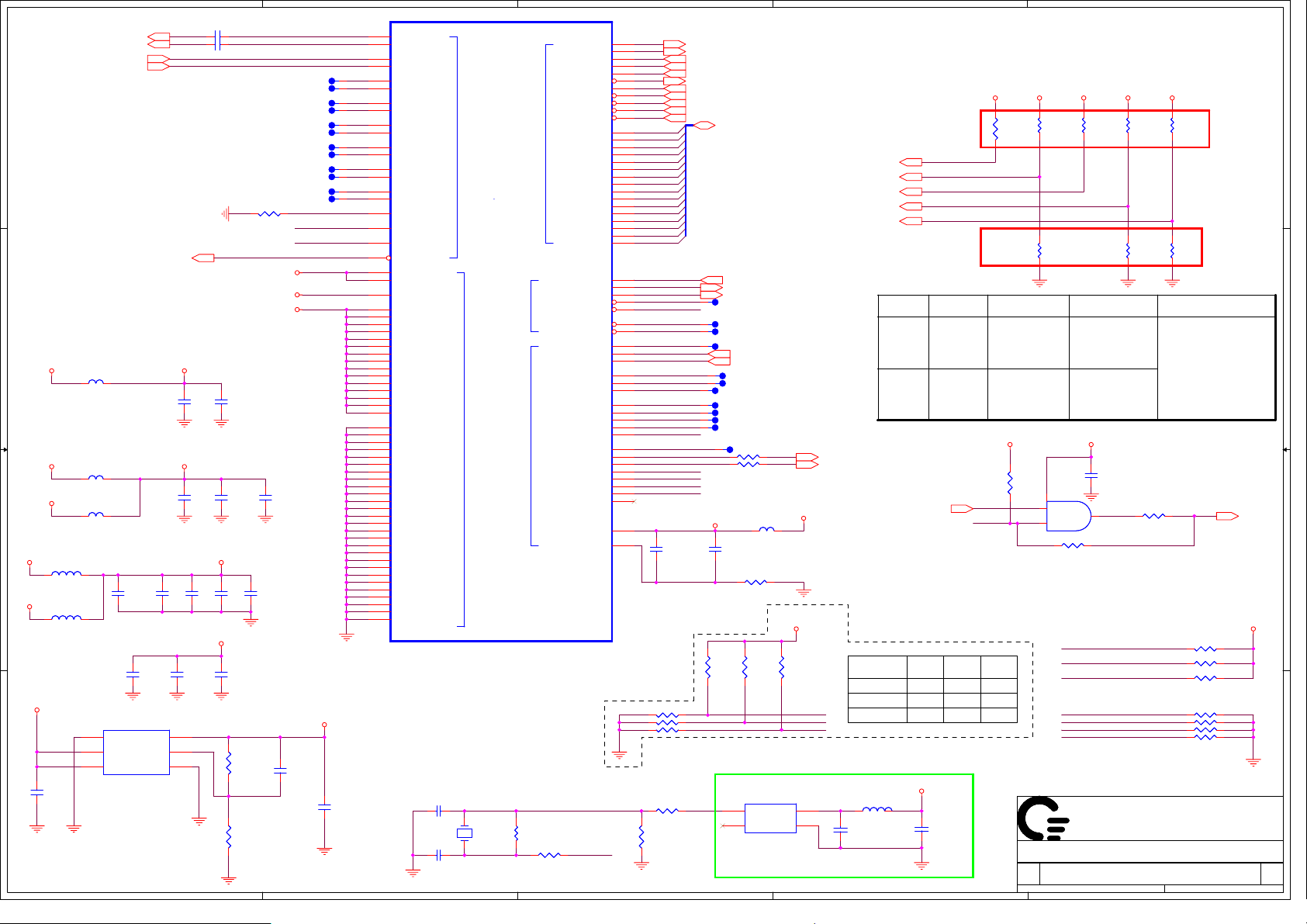
5
C712
C712
0.1U
0.1U
10
10
C722
C722
22U
22U
0805
0805
1
2
SATA_SBTX_DRX_P0
SATA_SBTX_DRX_N0
SATA_SBRX_DTX_N0
SATA_SBRX_DTX_P0
T60T60
T73T73
T68T68
T64T64
T172T172
T175T175
T169T169
T71T71
T62T62
T69T69
T70T70
T63T63
SATA_CAL
1%
1%
SATA_X1
SATA_X2
X5R6.3
X5R6.3
+1.25V_SATA_VCC
C733
C733
2200P_NC
2200P_NC
50 X7R
50 X7R
12
C731
C731
1U_NC
1U_NC
6.3 X5R
6.3 X5R
SATA_SBTX_C_DRX_P027
SATA_SBTX_C_DRX_N027
SATA_SBRX_DTX_N027
SATA_SBRX_DTX_P027
D D
C C
SATA Power
+3.3V_RUN
L75 BLM15AG221SN1DL75 BLM15AG221SN1D
CAP CLOSE TO THE
BALL OF SB600
+1.2V_RUN
L76
L76
BLM15AG221SN1D
BLM15AG221SN1D
+1.25V_SATA_VCC
L77
L77
BLM15AG221SN1D_NC
BLM15AG221SN1D_NC
+1.2V_RUN
B B
L79
L79
0805
0805
BLM21PG221SN1D
BLM21PG221SN1D
+1.25V_SATA_VCC
L78
L78
0805
0805
BLM21PG221SN1D_NC
BLM21PG221SN1D_NC
+3.3V_RUN
12
A A
C730
C730
2.2U_NC
2.2U_NC
10 X5R
10 X5R
0603
0603
3
2
1
U34
U34
GND1
IN
EN
12
C726
C726
22U
22U
6.3
6.3
X5R
X5R
0805
0805
RESET#/FB
TPS72501_NC
TPS72501_NC
C397 0.01U_16VC397 0.01U_16V
C396 0.01U_16VC396 0.01U_16V
SATA_ACT#40
+3.3V_XTLVDD_SATA
+1.2V_PLLVDD_SATA
C718
C718
1U
1U
6.3
6.3
C717
C717
0.1U_NC
0.1U_NC
10
10
4
OUT
5
6
GND2
5
C707
C707
1U
1U
10
10
0603
0603
X6S
X6S
C716
C716
1U
1U
6.3
6.3
+1.2V_AVDD_SATA
C715
C715
1U
1U
6.3
6.3
+1.2V_AVDD_SATA
C723
C723
0.1U_NC
0.1U_NC
10
10
R627 1K
R627 1K
+1.2V_PLLVDD_SATA
+3.3V_XTLVDD_SATA
+1.2V_AVDD_SATA
C708
C708
0.1U_NC
0.1U_NC
10
10
C710
C710
0.1U_NC
0.1U_NC
10
10
C714
C714
0.1U
0.1U
10
10
C711
C711
0.1U_NC
0.1U_NC
10
10
12
R645
R645
1.37K_NC
1.37K_NC
1%
1%
12
R646
R646
66.5K_NC
66.5K_NC
1%
1%
AH21
AJ21
AH20
AJ20
AH18
AJ18
AH17
AJ17
AH13
AH14
AH16
AJ16
AJ11
AH11
AH12
AJ13
AF12
AD16
AD18
AC12
AD14
AJ10
AC16
AE14
AE16
AE18
AE19
AF19
AF21
AG22
AG23
AH22
AH23
AJ12
AJ14
AJ19
AJ22
AJ23
AB14
AB16
AB18
AC14
AC18
AC19
AD12
AD19
AD21
AE12
AE21
AF11
AF14
AF16
AF18
AG11
AG12
AG13
AG14
AG16
AG17
AG18
AG19
AG20
AG21
AH10
AH19
4
U23B
U23B
SB600 A13
SB600 A13
4
SB600 SB 27x27mm
SATA_TX0+
SATA_TX0-
SATA_RX0SATA_RX0+
SATA_TX1+
SATA_TX1-
SATA_RX1SATA_RX1+
SATA_TX2+
SATA_TX2-
SATA_RX2SATA_RX2+
SATA_TX3+
SATA_TX3-
SATA_RX3SATA_RX3+
SATA_CAL
SATA_X1
SATA_X2
SATA_ACT#/GPIO67
PLLVDD_SATA_1
PLLVDD_SATA_2
XTLVDD_SATA
AVDD_SATA_1
AVDD_SATA_2
AVDD_SATA_3
AVDD_SATA_4
AVDD_SATA_5
AVDD_SATA_6
AVDD_SATA_7
AVDD_SATA_8
AVDD_SATA_9
AVDD_SATA_10
AVDD_SATA_11
AVDD_SATA_12
AVDD_SATA_13
AVDD_SATA_14
AVDD_SATA_15
AVSS_SATA_1
AVSS_SATA_2
AVSS_SATA_3
AVSS_SATA_4
AVSS_SATA_5
AVSS_SATA_6
AVSS_SATA_7
AVSS_SATA_8
AVSS_SATA_9
AVSS_SATA_10
AVSS_SATA_11
AVSS_SATA_12
AVSS_SATA_13
AVSS_SATA_14
AVSS_SATA_15
AVSS_SATA_16
AVSS_SATA_17
AVSS_SATA_18
AVSS_SATA_19
AVSS_SATA_20
AVSS_SATA_21
AVSS_SATA_22
AVSS_SATA_23
AVSS_SATA_24
AVSS_SATA_25
AVSS_SATA_26
AVSS_SATA_27
SB600 SB 27x27mm
Part 2 of 4
Part 2 of 4
SERIAL ATA
SERIAL ATA
SERIAL ATA POWER
SERIAL ATA POWER
SATA clock Option
C725 27P_50VC725 27P_50V
C724 27P_50VC724 27P_50V
21
Y6
Y6
25MHZ
25MHZ
20ppm
20ppm
EP 20pF
EP 20pF
SATA_X2_R
3
AB29
IDE_IORDY
AA28
IDE_IRQ
AA29
IDE_A0
AB27
IDE_A1
Y28
IDE_A2
AB28
IDE_DACK#
AC27
IDE_DRQ
AC29
IDE_IOR#
AC28
IDE_IOW#
W28
IDE_CS1#
W27
IDE_CS3#
IDE_D0/GPIO15
IDE_D1/GPIO16
IDE_D2/GPIO17
IDE_D3/GPIO18
IDE_D4/GPIO19
IDE_D5/GPIO20
IDE_D6/GPIO21
ATA 66/100
ATA 66/100
IDE_D7/GPIO22
IDE_D8/GPIO23
IDE_D9/GPIO24
IDE_D10/GPIO25
IDE_D11/GPIO26
IDE_D12/GPIO27
IDE_D13/GPIO28
IDE_D14/GPIO29
IDE_D15/GPIO30
SPI_DI/GPIO12
SPI_DO/GPIO11
SPI_CLK/GPIO47
SPI_HOLD#/GPIO31
SPI_CS#/GPIO32
LAN_RST#/GPIO13
ROM_RST#/GPIO14
SPI ROMHW MONITOR
SPI ROMHW MONITOR
FANOUT0/GPIO3
FANOUT1/GPIO48
FANOUT2/GPIO49
FANIN0/GPIO50
FANIN1/GPIO51
FANIN2/GPIO52
TEMP_COMM
TEMPIN0/GPIO61
TEMPIN1/GPIO62
TEMPIN2/GPIO63
TEMPIN3/TALERT#/GPIO64
VIN0/GPIO53
VIN1/GPIO54
VIN2/GPIO55
VIN3/GPIO56
VIN4/GPIO57
VIN5/GPIO58
VIN6/GPIO59
VIN7/GPIO60
AVDD
AVSS
Rev.A21
SATA_X1 VCC_Y6
R641
R641
10M
10M
R635 0R635 0
SATA_X2
IDE_DD0
AD28
IDE_DD1
AD26
IDE_DD2
AE29
IDE_DD3
AF27
IDE_DD4
AG29
IDE_DD5
AH28
IDE_DD6
AJ28
IDE_DD7
AJ27
IDE_DD8
AH27
IDE_DD9
AG27
IDE_DD10
AG28
IDE_DD11
AF28
IDE_DD12
AF29
IDE_DD13
AE28
IDE_DD14
AD25
IDE_DD15
AD29
SB_EC_SPI_DIN
J3
SB_EC_SPI_DO
J6
SB_EC_SPI_CLK
G3
G2
SPI_CS#
G6
C23
G5
M4
PCIE_MCARD1_DET#
T3
V4
PCIE_WWAN_DET#
N3
USB_WWAN_DET#
P2
W4
P5
P7
P8
T8
TALERT#
T7
WWAN_PCIE_RST#WWAN_PCIE_RST#WWAN_PCIE_RST#WWAN_PCIE_RST#WWAN_PCIE_RST#WWAN_PCIE_RST#
V5
WLAN_PCIE_RST#WLAN_PCIE_RST#WLAN_PCIE_RST#WLAN_PCIE_RST#WLAN_PCIE_RST#WLAN_PCIE_RST#
L7
LOM_PCIE_RST#
M8
NC_GPIO56
V6
LBF_ID0
M6
LBF_ID1
P4
LBF_ID2
M7
V7
N1
20mil Width
M1
HWM_AGND TRACE AT
LEAST 10MIL WIDE
R601 10KR601 10K
R597 10KR597 10K
R595 10KR595 10K
R634 33_F_NCR634 33_F_NC
3
C693
C693
2.2U
2.2U
10
10
0603
0603
HWM_AGND
R640
R640
49.9_F_NC
49.9_F_NC
IDE_DIORDY 27
IDE_IRQ 27
IDE_DA0 27
IDE_DA1 27
IDE_DA2 27
IDE_DDACK# 27
IDE_DDREQ 27
IDE_DIOR# 27
IDE_DIOW# 27
IDE_DCS1# 27
IDE_DCS3# 27
IDE_DD[0..15] 27
SB_EC_SPI_DIN 39
SB_EC_SPI_DO 39
SB_EC_SPI_CLK 39
T54T54
T46T46
T142T142
T148T148
PCIE_MCARD1_DET# 35
USB_MCARD1_DET# 35
T152T152
T147T147
T156T156
T150T150
T149T149
T151T151
T153T153
R349 0_NCR349 0_NC
R351 0_NCR351 0_NC
+3.3V_AVDD_HWM
C691
C691
0.1U_10V
0.1U_10V
R609 0R609 0
Close to SB600
R605
R605
10K_NC
10K_NC
For First build ,If next build no
use remove from BOM.
R_3COM_25ML
BIOS should not enable the
internal GPIO pull up resistor
T155T155
+3.3V_RUN
L72 BLM15AG221SN1DL72 BLM15AG221SN1D
+3.3V_RUN
R602
R602
R594
R594
10K_NC
10K_NC
10K_NC
10K_NC
LBF_ID0
LBF_ID1
LBF_ID2
Y3
Y3
3
VCC
OUT
1
VSS
OE
25MHZ_OSC_NC
25MHZ_OSC_NC
AC_SDATA_OUT24
CLK_PCI_DOCK23,36
CLK_PCI_PCCARD23,32
SB_WLAN_PCIE_RST# 35
SB_LOM_PCIE_RST# 30
BLM18AG121SN1D_0603_NC
4
2
BLM18AG121SN1D_0603_NC
2
15K internal PU for RTC_CLK
,External PU/PD is not required.
SB600 has 15K internal PD for AC_SDOUT
PCI_CLK023
PCI_CLK123
Net Name
PULL
HIGH
PULL
LOW
SIO_SPI_CS#39
Memory Vendor LBF_ID1 LBF_ID0LBF_ID2
Hynix
Qimonda
Samsung
C395
C395
0.1U_NC
0.1U_NC
L42
L42
00
0
0
+3.3V_RUN
2
+3.3V_RUN +3.3V_RUN +3.3V_RUN +3.3V_RUN +3.3V_RUN
R607
R607
2.2K_NC
2.2K_NC
AC_SDOUT
USE
DEBUG
STRAPS
IGNORE
DEBUG
STRAPS
Default
C394
C394
0.1U_NC
0.1U_NC
CLK_PCI_DOCK CLK_PCI_PCCARD
USE INT.
PLL48
USE EXT.
48MHZ
Default
+3.3V_SUS
R347
R347
1K_NC
1K_NC
1 2
SPI_CS#
0
1
2
1
R350 0R350 0
0
1
0
Title
Title
Title
Size Document Number Rev
Size Document Number Rev
Size Document Number Rev
Date: Sheet
Date: Sheet
Date: Sheet
1
REQUIRED
STRAPS
R366
R366
R363
R363
R621
R621
R610
10K_NC
10K_NC
10K
10K
R368
R368
10K
10K
CPU IF=K8
Default
CPU IF=P4
+3.3V_ALW
C382
C382
0.1U_NC
0.1U_NC
16
5
U22
U22
74AHC1G08GW_NC
74AHC1G08GW_NC
SB600M HDD/POWER
SB600M HDD/POWER
SB600M HDD/POWER
MGD 3A
MGD 3A
MGD 3A
16
R352 15_NCR352 15_NC
4
TALERT#
PCIE_MCARD1_DET#
USB_MCARD1_DET#
NC_GPIO56
WWAN_PCIE_RST#
WLAN_PCIE_RST#
LOM_PCIE_RST#
QUANTA
QUANTA
QUANTA
COMPUTER
COMPUTER
COMPUTER
10K
10K
R620
R620
10K_NC
10K_NC
PCI_CLK0 PCI_CLK1
H, H = PCI ROM
H, L = SPI ROM
L, H = LPC ROM
L, L = FWH ROM
R614 10KR614 10K
R615 100KR615 100K
R618 100KR618 100K
R628 20KR628 20K
R613 20KR613 20K
R598 20KR598 20K
R604 20KR604 20K
1
R610
10K_NC
10K_NC
R612
R612
10K
10K
1 2
1 2
Default
SPI_CS0# 37
+3.3V_RUN
of
of
of
25 89Thursday, March 01, 2007
25 89Thursday, March 01, 2007
25 89Thursday, March 01, 2007
Page 26
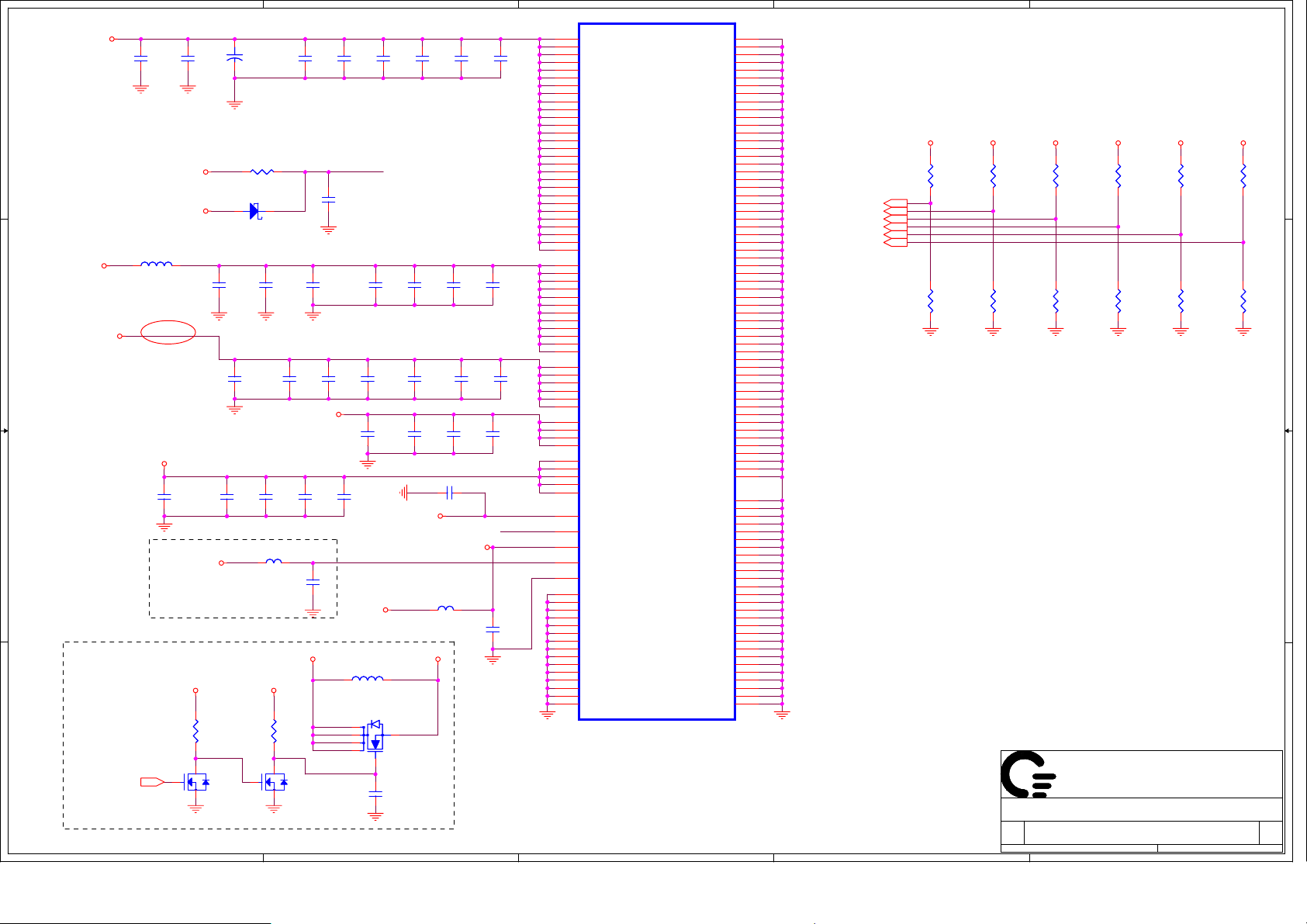
5
+3.3V_RUN
D D
+1.2V_RUN
C C
B B
A A
+3.3V_SUS
1.2V_SUS_ON39
12
12
C705
C705
0.1U_NC
0.1U_NC
10
10
±10
±10
X7R
X7R
L80
L80
1 2
FBMJ4516HS111-T
FBMJ4516HS111-T
Note: FBMJ4516HS111-T
was 110 ohm@100MHz
4A DC 0.014ohm
%
%
+5V_RUN
+3.3V_RUN
A00-01
C700
C700
0.1U_NC
0.1U_NC
10
10
±10
±10
X7R
X7R
Put very close
+1.2V_SUS
C655
C655
22U
22U
6.3
6.3
0805
0805
X5R
X5R
SB600 ONLY
+1.2V_RUN
20mil Width
+3.3V_ALW2
1 2
31
2
5
+
+
C398
C398
220U_6.3V_7343
220U_6.3V_7343
%
%
R644 1KR644 1K
D30
D30
SDMK0340L-7-F
SDMK0340L-7-F
12
C696
C696
0.1U_NC
0.1U_NC
10
10
±10
%
±10
%
X7R
X7R
C353
C353
22U
22U
6.3
6.3
0805
0805
X6S
X6S
20%
20%
20mil Width
C665
C665
0.1U_10V
0.1U_10V
BLM15AG221SN1D
BLM15AG221SN1D
R314
R314
100K
100K
1.2V_SUS_ON#
Q40
Q40
2N7002W-7-F
2N7002W-7-F
C676
C676
1U
1U
6.3
6.3
+V5_VREF1
C727
C727
1U
1U
6.3
6.3
+1.2V_RUN_VDD
C695
12
C692
C692
0.1U_NC
0.1U_NC
10
10
±10
±10
X7R
X7R
C695
22U
22U
6.3
6.3
0805
0805
%
%
X6S
X6S
20%
20%
50mil Width
C675
C675
C687
C687
1U
1U
1U
1U
6.3
6.3
6.3
6.3
+1.2V_ALW_SUS
20mil Width
C673
C673
C664
C664
0.1U_10V
0.1U_10V
0.1U_10V
0.1U_10V
L70
L70
C660
C660
2.2U
2.2U
10
10
0603
0603
+1.2V_ALW_SUS +1.2V_SUS
+15V_ALW
2
R590
R590
100K
100K
1 2
31
BLM21PG221SN1D_NC 0805
BLM21PG221SN1D_NC 0805
Q69
Q69
2N7002W-7-F
2N7002W-7-F
C709
C709
1U
1U
6.3
6.3
12
C669
C669
0.1U_10V
0.1U_10V
+1.2V_AVDDCK
+3.3V_RUN
L68
L68
6
5
2
1
4
C720
C720
1U
1U
6.3
6.3
C688
C688
1U
1U
10
10
0603
0603
X6S
X6S
±10
%
±10
%
C658
C658
0.1U
0.1U
10
10
±10
%
±10
%
X7R
X7R
C681
C681
0.1U_10V
0.1U_10V
+1.8V_RUN
Q70
Q70
4
SI3456DV-T1-E3
SI3456DV-T1-E3
3
C662
C662
4700P
4700P
25
25
4
20mil Width
C719
C719
C721
C721
1U
1U
1U
1U
6.3
6.3
6.3
6.3
C701
C701
C689
C689
1U
1U
1U
1U
10
10
10
10
0603
0603
0603
0603
X6S
X6S
X6S
X6S
±10
%
±10
±10
±10
12
C373
C373
0.1U
0.1U
10
10
±10
±10
X7R
X7R
C685
C685
0.1U_10V
0.1U_10V
C706 0.1U_10VC706 0.1U_10V
+3.3V_AVDDCK
BLM15AG221SN1D
BLM15AG221SN1D
%
%
%
12
C640
C640
0.1U
0.1U
10
10
%
%
±10
%
±10
%
X7R
X7R
C678
C678
0.1U_10V
0.1U_10V
L71
L71
C713
C713
1U
1U
6.3
6.3
C702
C702
1U
1U
10
10
0603
0603
X6S
X6S
±10
%
±10
%
12
C682
C682
0.1U
0.1U
10
10
±10
±10
X7R
X7R
C674
C674
0.1U_10V
0.1U_10V
+V5_VREF1
C661
C661
2.2U
2.2U
10
10
0603
0603
3
U23C
U23C
A25
SB600 SB 27x27mm
SB600 SB 27x27mm
VDDQ_1
A28
VDDQ_2
C29
VDDQ_3
D24
VDDQ_4
L9
VDDQ_5
L21
VDDQ_6
M5
VDDQ_7
P3
VDDQ_8
P9
VDDQ_9
T5
VDDQ_10
V9
VDDQ_11
W2
VDDQ_12
W6
VDDQ_13
W21
VDDQ_14
W29
VDDQ_15
AA12
VDDQ_16
AA16
VDDQ_17
AA19
VDDQ_18
AC4
VDDQ_19
AC23
VDDQ_20
AD27
VDDQ_21
AE1
VDDQ_22
AE9
VDDQ_23
AE23
VDDQ_24
AH29
VDDQ_25
AJ2
VDDQ_26
AJ6
VDDQ_27
AJ26
VDDQ_28
M13
VDD_1
M17
VDD_2
N12
VDD_3
N15
VDD_4
N18
VDD_5
R13
VDD_6
R17
VDD_7
U12
VDD_8
U15
VDD_9
U18
VDD_10
V13
VDD_11
V17
VDD_12
A2
S5_3.3V_1
A7
S5_3.3V_2
F1
S5_3.3V_3
J5
A18
A19
B19
B20
B21
AA27
AE11
A24
A22
B22
V29
V28
V27
V26
V25
V24
V23
V22
U27
T29
T28
T27
T24
T21
P27
J7
K1
G4
H1
H2
H3
S5_3.3V_4
S5_3.3V_5
S5_3.3V_6
S5_1.2V_1
S5_1.2V_2
S5_1.2V_3
S5_1.2V_4
USB_PHY_1.2V_1
USB_PHY_1.2V_2
USB_PHY_1.2V_3
USB_PHY_1.2V_4
USB_PHY_1.2V_5
CPU_PWR
V5_VREF
AVDDCK_3.3V
AVDDCK_1.2V
AVSSCK
PCIE_VSS_42
PCIE_VSS_41
PCIE_VSS_40
PCIE_VSS_39
PCIE_VSS_38
PCIE_VSS_37
PCIE_VSS_36
PCIE_VSS_35
PCIE_VSS_34
PCIE_VSS_33
PCIE_VSS_32
PCIE_VSS_31
PCIE_VSS_30
PCIE_VSS_29
PCIE_VSS_28
SB600 A13
SB600 A13
%
%
Part 3 of 4
Part 3 of 4
POWER
POWER
3
PCIE_VSS_1
PCIE_VSS_2
PCIE_VSS_3
PCIE_VSS_4
PCIE_VSS_5
PCIE_VSS_6
PCIE_VSS_7
PCIE_VSS_8
PCIE_VSS_9
PCIE_VSS_10
PCIE_VSS_11
PCIE_VSS_12
PCIE_VSS_13
PCIE_VSS_14
PCIE_VSS_15
PCIE_VSS_16
PCIE_VSS_17
PCIE_VSS_18
PCIE_VSS_19
PCIE_VSS_20
PCIE_VSS_21
PCIE_VSS_22
PCIE_VSS_23
PCIE_VSS_24
PCIE_VSS_25
PCIE_VSS_26
PCIE_VSS_27
VSS_1
VSS_2
VSS_3
VSS_4
VSS_5
VSS_6
VSS_7
VSS_8
VSS_9
VSS_10
VSS_11
VSS_12
VSS_13
VSS_14
VSS_15
VSS_16
VSS_17
VSS_18
VSS_19
VSS_20
VSS_21
VSS_22
VSS_23
VSS_24
VSS_25
VSS_26
VSS_27
VSS_28
VSS_29
VSS_30
VSS_31
VSS_32
VSS_33
VSS_34
VSS_35
VSS_36
VSS_37
VSS_38
VSS_39
VSS_40
VSS_41
VSS_42
VSS_43
VSS_44
VSS_45
VSS_46
VSS_47
VSS_48
VSS_49
VSS_50
VSS_51
VSS_52
VSS_53
VSS_54
VSS_55
VSS_56
VSS_57
Rev.A21
A1
A20
A21
A29
B1
B7
B25
C21
C22
C24
D6
E24
F2
F23
G1
J1
J8
L6
L8
M9
M12
M15
M18
N13
N17
P1
P6
P21
R12
R15
R18
T6
T9
U13
U17
V3
V8
V12
V15
V18
V21
W1
W9
Y29
AA11
AA14
AA18
AC6
AC24
AD9
AD23
AE3
AE27
AG6
AJ1
AJ25
AJ29
D27
D28
D29
F26
G23
G24
G25
H27
J23
J26
J28
K27
L22
L23
L24
L27
L28
M21
M24
M27
N27
N28
P22
P23
P24
P25
P26
PCI_AD2823,32
PCI_AD2723,32
PCI_AD2623,32
PCI_AD2523,32
PCI_AD2423,32
PCI_AD2323,32
2
+3.3V_RUN +3.3V_RUN +3.3V_RUN +3.3V_RUN +3.3V_RUN +3.3V_RUN
12
R630
R630
10K_NC
10K_NC
12
R633
R633
2.2K_NC
2.2K_NC
2
12
R636
R636
10K_NC
10K_NC
12
R637
R637
2.2K_NC
2.2K_NC
Title
Title
Title
Size Document Number Rev
Size Document Number Rev
Size Document Number Rev
Date: Sheet
Date: Sheet
Date: Sheet
12
R624
R624
10K_NC
10K_NC
12
R626
R626
2.2K_NC
2.2K_NC
QUANTA
QUANTA
QUANTA
COMPUTER
COMPUTER
COMPUTER
SB600M Power & STRAPS
SB600M Power & STRAPS
SB600M Power & STRAPS
MGD 3A
MGD 3A
MGD 3A
12
R639
R639
10K_NC
10K_NC
12
R638
R638
2.2K_NC
2.2K_NC
1
12
R629
R629
10K_NC
10K_NC
12
R632
R632
2.2K_NC
2.2K_NC
26 89Thursday, March 01, 2007
26 89Thursday, March 01, 2007
26 89Thursday, March 01, 2007
of
of
1
of
12
12
R643
R643
10K_NC
10K_NC
R642
R642
2.2K_NC
2.2K_NC
Page 27
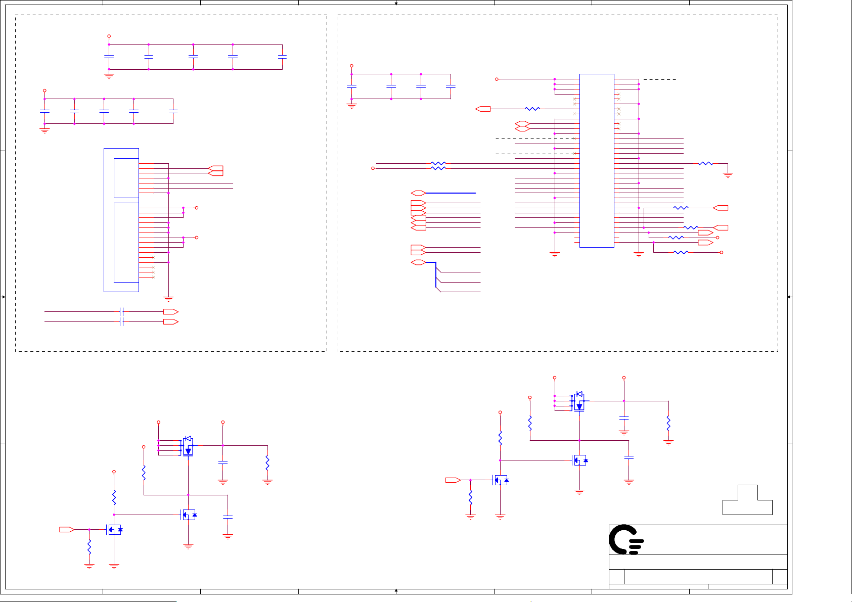
1
2
3
4
5
6
7
8
SATA Connector.
A A
B B
Place caps close to
+5V_HDD
connector.
12
C738
C738
0.1U_16V
0.1U_16V
SATA_SBRX_C_DTX_N0
SATA_SBRX_C_DTX_P0
12
C740
C740
1000P_50V
1000P_50V
+3.3V_RUN
12
C735
C735
0.1U_16V_NC
0.1U_16V_NC
12
C739
C739
0.1U_16V
0.1U_16V
CON6
CON6
MLX_67492-1821
MLX_67492-1821
1 2
1 2
GND1
RXP
RXN
GND2
TXN
TXP
GND3
3.3V_0
3.3V_1
3.3V_2
GND4
GND5
GND6
5V_0
5V_1
5V_2
GND7
RSVD
GND8
12V_0
12V_1
12V_2
12
12
C741
C741
10U_10V_0805
10U_10V_0805
1
2
3
4
5
6
7
8
9
10
11
12
13
14
15
16
17
18
19
20
21
22
C728
C728
0.01U16X7R
0.01U16X7R
C729
C729
0.01U16X7R
0.01U16X7R
C732
C732
1000P_50V_NC
1000P_50V_NC
12
C734
C734
0.1U_16V_NC
0.1U_16V_NC
Place caps close to
connector.
12
C742
C742
1U_10V_0603
1U_10V_0603
SATA_SBRX_C_DTX_N0
SATA_SBRX_C_DTX_P0
+3.3V_RUN
+5V_HDD
SATA_SBRX_DTX_N0 25
SATA_SBRX_DTX_P0 25
NOTE:
C728,C729 Close to CON6
12
C737
C737
10U_10V_0805_NC
10U_10V_0805_NC
SATA_SBTX_C_DRX_P0 25
SATA_SBTX_C_DRX_N0 25
12
C736
C736
1U_10V_0603_NC
1U_10V_0603_NC
ODD Connector.
+5V_MOD
12
C113
C113
10U_10V_0805
10U_10V_0805
+3.3V_RUN
12
Place caps close to
connector.
IDE_DDACK#
IDE_DD[0..15]25
IDE_DDREQ25
IDE_DIOW#25
IDE_DIOR#25
IDE_DIORDY25
IDE_DDACK#25
IDE_IRQ25
IDE_DCS1#25
IDE_DCS3#25
IDE_DA[0..2]25
12
C109
C109
C97
C97
0.1U_16V
0.1U_16V
0.1U_16V
0.1U_16V
R103 0R103 0
R106 4.7KR106 4.7K
12
C110
C110
0.1U_16V
0.1U_16V
SATA_DET#24
12
12
IDE_DD[0..15]
IDE_DDREQ
IDE_DIOW#
IDE_DIOR#
IDE_DIORDY
IDE_DDACK#
IDE_IRQ
IDE_DCS1#
IDE_DCS3#
IDE_DA0
IDE_DA1
IDE_DA2
+5V_MOD
DASP#
PDIAG#
R97 0_NCR97 0_NC
USBP4+24
USBP4-24
IDE_DCS1#
IDE_IRQ
IDE_DDACK_R#
IDE_DDREQ
IDE_DD0
IDE_DD14
IDE_DD13
IDE_DD3
IDE_DD4
IDE_DD10
IDE_DD9
IDE_DD7
JMOD1
JMOD1
1
1
3
3
5
5
7
7
9
9
11
11
13
12
13
15
15
17
17
19
19
21
21
23
23
25
25
27
27
29
29
31
31
33
33
35
35
37
37
39
39
41
41
43
43
45
45
47
47
49
49
51
51
53
53
55
55
57
57
59
59
61
61
63
63
65
65
67
67
JAE_WM1F068NSD-R500
JAE_WM1F068NSD-R500
2
2
4
4
6
6
8
8
10
10
12
12
14
14
16
16
18
18
20
20
22
22
24
24
26
26
28
28
30
30
32
32
34
34
36
36
38
38
40
40
42
42
44
44
46
46
48
48
50
50
52
52
54
54
56
56
58
58
60
60
62
64
66
68
MOD_RST
MOD_RST
62
64
66
68
INT_MOD_IN1#
IDE_DCS3#
IDE_DA2
IDE_DA0
IDE_DA1
R105 470R105 470
CSEL2
IDE_DIOR#IDE_DIORDY
IDE_DIOW#
IDE_DD15
IDE_DD1
IDE_DD2
IDE_DD12
IDE_DD11
R119 0_NCR119 0_NC
IDE_DD5
IDE_DD6
IDE_DD8
R121 100KR121 100K
R122 100KR122 100K
1 2
12
R118 56R118 56
PLTRST# 23,38,39,43
IDE_RST_MOD 24
USB_IDE# 24
+3.3V_RUN
MODPRES# 38
+3.3V_ALW
C C
Q14
Q14
FDC655BN
R93
R93
100K
100K
FDC655BN
6
5
2
1
3
31
2
6
+15V_ALW
12
R104
R104
100K
100K
+3.3V_ALW2
12
31
2
R102
R102
100K
100K
Q17
Q17
2N7002W-7-F
2N7002W-7-F
Vgs = 20
Vgs = 20
Vds = 60
Vds = 60
Current = 115m
Current = 115m
Type = Single N
Type = Single N
1 2
4
3
HDD_EN_5V
31
Q72
Q72
2N7002W-7-F
2N7002W-7-F
Vgs = 20
Vgs = 20
Vds = 60
Vds = 60
Current = 115m
Current = 115m
Type = Single N
Type = Single N
+5V_HDD+5V_ALW
Q45
Q45
FDC655BN
FDC655BN
+15V_ALW
+3.3V_ALW2
12
R648
R648
100K
100K
D D
HDDC_EN38
1
31
Q71
Q71
2
12
2N7002W-7-F
2N7002W-7-F
R647
R647
Vgs = 20
Vgs = 20
100K
100K
Vds = 60
Vds = 60
Current = 115m
Current = 115m
Type = Single N
Type = Single N
6
5
2
1
R374
R374
100K
100K
1 2
2
2
Design current: 700mA
Max current: 1000mA
12
C399
C399
4.7U_6.3V_0603
4.7U_6.3V_0603
12
C400
C400
0.1U_50V_0603
0.1U_50V_0603
12
R375
R375
100K
100K
3
MODC_EN38
4
5
+5V_MOD+5V_ALW
Design current: 1050mA
Max current: 1500mA
4
12
C106
C106
10U_10V_0805
10U_10V_0805
MOD_EN
Q15
Q15
2N7002W-7-F
2N7002W-7-F
Vgs = 20
Vgs = 20
Vds = 60
Vds = 60
Current = 115m
Current = 115m
Type = Single N
Type = Single N
12
C114
C114
0.1U_50V_0603
0.1U_50V_0603
Title
Title
Title
SATA (HDD&CD_ROM)
SATA (HDD&CD_ROM)
SATA (HDD&CD_ROM)
Size Document Number Rev
Size Document Number Rev
Size Document Number Rev
MGD 2A
MGD 2A
MGD 2A
Date: Sheet
Date: Sheet
Date: Sheet
12
R79
R79
100K
100K
QUANTA
QUANTA
QUANTA
COMPUTER
COMPUTER
COMPUTER
7
Symbol:
2N7002W-7-F
D(3)
G(2)
of
of
of
27 89Thursday, March 01, 2007
27 89Thursday, March 01, 2007
27 89Thursday, March 01, 2007
8
S(1)
Page 28

1
2
3
4
5
6
7
8
GDS
231
2N7002W-7-F
A A
AUDIO_AVDD_ON AUD_AMP_MUTE#
B B
C C
D D
AUD_SPK_ENABLE#
AUD_EAPD
NB_MUTE#
+VDDA
+3.3V_RUN
+3.3V_RUN
R654
R654
SB_AZ_CODEC_BITCLK
R293
R293
47_NC
47_NC
1 2
C299
C299
0.1U_10V_NC
0.1U_10V_NC
1 2
SB_AZ_CODEC_SDOUT
R289
R289
47_NC
47_NC
1 2
C294
C294
0.1U_NC
0.1U_NC
10
10
1 2
%
%
±10
±10
X7R
X7R
0402
0402
Package 1206 for THD+N
performance for Vista Logo
requirements.
AUD_HP_OUT_L
AUD_HP_OUT_R
+5V_SPK_AMP
R576
R576
0_NC
0_NC
1 2
+5V_SPK_AMP
2
Q37
Q37
2N7002W-7-F
2N7002W-7-F
2
Q36
Q36
2N7002W-7-F
2N7002W-7-F
R290 10KR290 10K
1 2
R294 10KR294 10K
1 2
R274 10K_NCR274 10K_NC
1 2
R671 10KR671 10K
100K
100K
1 2
DVDD_CORE_40
12
Close to
U16 pin 6.
Close to
U16 pin 5.
1
C756
C756
1000P_50V
1000P_50V
C654 0.033U 1206200 X7RC654 0.033U 1206200 X7R
C653 0.033U 1206200 X7RC653 0.033U 1206200 X7R
C342 1U 120616C342 1U 120616
C335 1U 120616C335 1U 120616
12
R570
R570
100K
100K
+5V_SPK_AMP
R312
R312
100K
100K
1 2
DOCK_HP_MUTE#
AUD_SPDIF_SHDN
AUD_EAPD
SB_AZ_CODEC_BITCLK24
SB_AZ_CODEC_SDIN024
SB_AZ_CODEC_SDOUT24
SB_AZ_CODEC_SYNC24
SB_AZ_CODEC_RST#24
AUD_SPDIF_OUT22,36
12
C314
C314
10U_10V_0805_NC
10U_10V_0805_NC
+VDDA
12
C273
C273
0.1U_10V
0.1U_10V
1 2
31
31
R313
R313
100K
100K
+3.3V_RUN
12
C336
C336
47P_50V_NC
47P_50V_NC
R573
R573
100K_NC
100K_NC
R568
R568
100K
100K
12
C313
C313
0.1U_10V
0.1U_10V
C309
C309
1U
1U
10
10
0603
0603
2
12
AUD_EAPD
12
C755
C755
100P_NC
100P_NC
C343
C343
47P_50V_NC
47P_50V_NC
+5V_SPK_AMP
R328
R328
100K
100K
AUD_AMP_GAIN1
AUD_AMP_GAIN2
R339Title
R339Title
100K_NC
100K_NC
R295 33R295 33
R651 0R651 0
1 2
R652 0R652 0
1 2
12
C754
C754
100P_NC
100P_NC
C271
C271
1U
1U
10
10
0603
0603
12
C315
C315
10U_10V_0805_NC
10U_10V_0805_NC
12
C369
C369
47P_50V_NC
47P_50V_NC
12
C334
C334
10U_10V_0805
10U_10V_0805
12
C372
C372
47P_50V_NC
47P_50V_NC
12
C351
C351
1U_10V_0603
1U_10V_0603
GAIN1 GAIN2 GAIN
1
0
11
SDIN
AUD_EAPD_SP
SPDIF_OUT
DVDD_CORE_40
6dB
10dB
15.6dB
21.6dB
6
8
5
10
11
46
2
4
47
48
43
44
45
1
9
40
3
25
38
7
26
42
49
00
0
1
12
+3.3V_RUN
12
C287
C287
0.1U_10V
0.1U_10V
3
LIN-AUD_LINE_OUT_L
RIN-AUD_LINE_OUT_R
HP_OUT_L
HP_OUT_R
C333 1U
C333 1U
10 0603
10 0603
1 2
AUD_SPK_ENABLE#
AUD_HP_EN
AUD_AMP_MUTE#
AUD_AMP_GAIN1
AUD_AMP_GAIN2
C344 1U
C344 1U
1 2
R6701MR670
1M
Default
AZALIA (HD) CODEC
U16
U16
HDA_BITCLK
HDA_SDI_CODEC
HDA_SDO
HDA_SYNC
HDA_RST#
DMIC_CLK
DMIC0/VOL_UP/GPIO1
DMIC1/VOL_DN/GPIO2
SPDIF_IN/EAPD/GPIO0
SPDIF_OUT
NC_43
NC_44
NC_45
DVDD_CORE_1
DVDD_CORE_9
DVDD_CORE_40
DVDD_IO
AVDD_25
AVDD_38
DVSS
AVSS_26
AVSS_42
GNDPAD
STAC9205 Rev.B2
STAC9205 Rev.B2
INTERNAL SPEAKER AMP
U20
U20
3
SPKR_INL
2
SPKR_INR
27
HP_INL
MAX9789A
MAX9789A
26
HP_INR
TQFN 32PIN
TQFN 32PIN
24
BIAS
23
SPKR_EN
22
HP_EN
25
MUTE
31
GAIN1
32
GAIN2
17
HPVDD
9
CPVDD
C1P
10
C1P
12
100603
100603
12
C341
C341
1U
1U
10
10
0603
0603
STAC9205
STAC9205
LQFP 48PIN
LQFP 48PIN
4
C1N
11
CPGND
14
PVSS
13
CPVSS
AUDIO_AVDD_ON
12
R5860R586
0
REGEN
12
C656
C656
0.47U_NC
0.47U_NC
16
16
Y5V
Y5V
0603
0603
For TPA6040A,pop
C374,depop R329
SENSE_A
SENSE_B
PORT_A_L
PORT_A_R
VREFOUT_A
PORT_B_L
PORT_B_R
VREFOUT_B
PORT_C_L
PORT_C_R
VREFOUT_C
PORT_D_L
PORT_D_R
PORT_E_L
PORT_E_R
GPIO4/VREFOUT_E
PORT_F_L
PORT_F_R
GPIO3/VREFOUT_F
CD_L
CD_GND
CD_R
PC_BEEP
MONO_OUT
VREFFILT
CAP2
For TPA6040A,pop
C656,depop R586
AUD_SENSE_A
13
AUD_SENSE_B
34
AUD_HP_OUT_L
39
AUD_HP_OUT_R
41
37
21
22
28
23
24
29
AUD_LINE_OUT_L
35
AUD_LINE_OUT_R
36
14
15
DOCK_HP_MUTE#
31
16
17
AUD_SPDIF_SHDN
30
18
19
20
AUD_PC_BEEP
12
32
VREFFILT
27
CAP2
33
5
OUTL+
OUTL-
OUTR+
OUTR-
HPL
HPR
REGEN
SET
VOUT
VDD
PVDD_8
PVDD_18
GND_28
PGND_5
PGND_21
MAX9789A
MAX9789A
AUDIO_AVDD_ON 19
SET
C374
C374
0.033U_16V_NC
0.033U_16V_NC
1 2
12
C316
C316
10U_10V_0805
10U_10V_0805
INT_SPK_L1
6
INT_SPK_L2
7
INT_SPK_R1
20
INT_SPK_R2
19
16
15
REGEN
4
SET
1
29
30
8
18
28
5
21
R3290R329
0
1 2
+VDDA
R287
R287
100K
100K
AUD_EXT_MIC_L 29
AUD_EXT_MIC_R 29
AUD_VREFOUT_B 29
AUD_INT_MIC_IN 29
DOCK_HP_MUTE# 38
AUD_SPDIF_SHDN 22,38
12
C321
C321
10U_10V_0805
10U_10V_0805
AUD_HP_JACK_L 29
AUD_HP_JACK_R 29
+VDDA
+5V_SPK_AMP
+5V_SPK_AMP
+5V_SPK_AMP
+5V_SPK_AMP
12
C348
C348
1U_10V_0603
1U_10V_0603
NB_MUTE#38
AUD_HP_NB_SENSE29,38
6
INT_SPK_R1
INT_SPK_R2
INT_SPK_L1
INT_SPK_L2
12
C350
C350
1U_10V_0603
1U_10V_0603
L41
L41
BLM21PG600SN1D_0805
BLM21PG600SN1D_0805
12
C370
C370
10U_10V_0805
10U_10V_0805
FB_60ohm+-25%_100MHz
_3A_0.05ohm DC
Layout Note:
Close to U16 Pin 13.
TRACE>15 mil
15 mils trace
C288
C288
12
100P
100P
%
%
±5
±5
50
50
EP
EP
X7R
X7R
+5V_SPK_AMP
12
C325
C325
1U_10V_0603
1U_10V_0603
+5V_RUN
12
Layout Note:
Place close to
pin 8.
AUD_HP_NB_SENSE
NB_MUTE#
AUD_HP_NB_SENSE
C306
C306
0.1U_16V
0.1U_16V
12
Title
Title
Title
Size Document Number Rev
Size Document Number Rev
Size Document Number Rev
Date: Sheet
Date: Sheet
Date: Sheet
C289
C289
12
100P
100P
%
%
±5
±5
50
50
EP
EP
X7R
X7R
12
C327
C327
0.1U_10V
0.1U_10V
Layout Note:
Place close
U20.
+5V_SPK_AMP
+5V_SPK_AMP
53
1
4
2
U19 74AHC1G08GWU19 74AHC1G08GW
R308
R308
39.2K_F
39.2K_F
2
Q38
Q38
2N7002W-7-F
2N7002W-7-F
R291
R291
20K
20K
BEEP2AUD_PC_BEEP BEEP1
1 2
12
R301
R301
10K_NC
10K_NC
QUANTA
QUANTA
QUANTA
COMPUTER
COMPUTER
COMPUTER
Azelia CODEC
Azelia CODEC
Azelia CODEC
MGD 3A
MGD 3A
MGD 3A
7
12
C326
C326
1U_10V_0603
1U_10V_0603
C329
C329
X7R
X7R
%
%
AUD_HP_EN
AUD_SENSE_A
12
31
C290
C290
12
100P
100P
%
%
±5
±5
50
50
EP
EP
X7R
X7R
0.1U
0.1U
12
10±10
10±10
12
R309
R309
20K_F
20K_F
31
Q39
Q39
2N7002W-7-F
2N7002W-7-F
4
+VDDA
0402
0402
2
+VDDA
JSPK1
JSPK1
1
1
2
2
3
3
4
4
MLX_53398-0471
MLX_53398-0471
C291
C291
12
100P
100P
%
%
±5
±5
50
50
EP
EP
X7R
X7R
12
Layout Note:
Place close U20.
12
C324
C324
10U_10V_0805
10U_10V_0805
12
12
C347
C347
1U_10V_0603
1U_10V_0603
Layout Note:
Place close to
pin 18.
C323
C323
1000P_50V
1000P_50V
C352
C352
1U_10V_0603
1U_10V_0603
12
R3105.11K
R3105.11K
1% 0402
1% 0402
AUD_MIC_SWITCH 29
Close to U16
C292
C292
0.1U_16V
0.1U_16V
12
53
1
SPKR 24
2
BEEP 39
U17
U17
74AHCT1G86GW
74AHCT1G86GW
of
of
of
28 89Thursday, March 01, 2007
28 89Thursday, March 01, 2007
28 89Thursday, March 01, 2007
8
+VDDA
Page 29
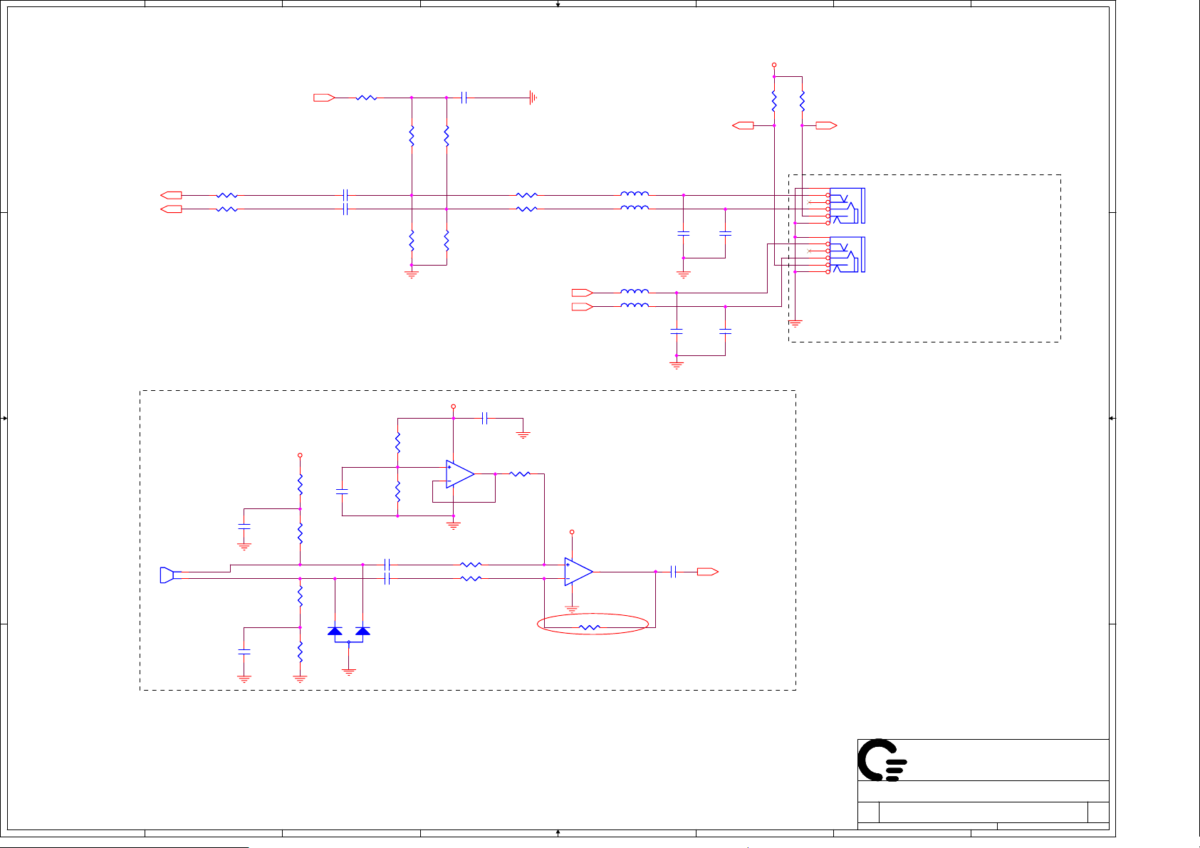
1
A A
AUD_EXT_MIC_L28
AUD_EXT_MIC_R28
B B
C C
M1
M1
A-OF6027ZGF-P3R6
A-OF6027ZGF-P3R6
2
AUD_VREFOUT_B28
R136 5.11 1%R136 5.11 1%
1 2
R139 5.11 1%R139 5.11 1%
1 2
INT_MIC_C_L+
12
C638
C638
2.2U_10V_0603
2.2U_10V_0603
1
2
INT_MIC_L-
INT_MIC_C_L-
12
C641
C641
2.2U_10V_0603
2.2U_10V_0603
MIC_L1
MIC_R1
+VDDA
12
R5741KR574
1K
12
R5831KR583
1K
12
R5711KR571
1K
12
R5721KR572
1K
3
R149 0R149 0
1 2
C168 1U 060310 X5RC168 1U 060310 X5R
MIC_L2
1 2
MIC_R2
1 2
C171 1U 060310 X5RC171 1U 060310 X5R
1 2
12
C355
C355
2.2U_10V_0603
2.2U_10V_0603
2
3
0.1U 10
0.1U 10
0.1U 10
0.1U 10
1
C657
C657
C643
C643
D17
D17
SM05_NC
SM05_NC
1 2
4
C173 10U 06036.3C173 10U 06036.3
12
12
R171
R171
R148
R148
4.7K
4.7K
4.7K
4.7K
R125 0R125 0
R130 0R130 0
R135
R135
R170
R170
20K_NC
20K_NC
20K_NC
20K_NC
1%
1%
1%
1%
AUD_HP_JACK_L28
AUD_HP_JACK_R28
+VDDA
C349 0.1U 16V
C349 0.1U 16V
Y5V
R326
R326
100K
100K
3
2
R327
R327
100K
100K
INT_MIC_L1+
INT_MIC_L1- INT_MIC_L2-
U21A
U21A
8
LM358ADR2G
LM358ADR2G
1
4
R584
R584
10K
10K
1 2
1 2
R569
R569
10K
10K
Y5V
R5850R585
0
INT_MIC_L2+INT_MIC_L+
5
L29
L29
BLM18BD601SN1D_0603
BLM18BD601SN1D_0603
1 2
L30
L30
1 2
BLM18BD601SN1D_0603
BLM18BD601SN1D_0603
L32,L33,L29,L30
FB_600ohm+-25%_100MHz
_200mA_0.65 ohm DC
L33
0603L33
0603
BLM18BD601SN1D
BLM18BD601SN1D
1 2
L32
0603L32
0603
1 2
BLM18BD601SN1D
BLM18BD601SN1D
+VDDA
U21B
U21B
8
LM358ADR2G
LM358ADR2G
5
6
R575 100K 1%R575 100K 1%
4
A00-08
INT_MIC_IN_OP
7
AUD_HP_NB_SENSE28,38
MIC_L3
MIC_R3
12
C136
C136
100P_50V
100P_50V
HP_SPK_L2
HP_SPK_R2
12
C201
C201
100P_50V
100P_50V
C639
C639
0.1U 10
0.1U 10
Only Single INT MIC
6
+3.3V_RUN
12
12
C132
C132
100P_50V
100P_50V
12
C194
C194
100P_50V
100P_50V
AUD_INT_MIC_IN 28
7
12
R188
R188
R120
R120
100K
100K
100K
100K
AUD_MIC_SWITCH 28
CON3
CON3
1
2
6
3
4
5
1
2
6
3
4
5
TYC_1775162-1
TYC_1775162-1
CON4
CON4
TYC_1775162-1
TYC_1775162-1
STEREO MIC
LINE IN
HEADPHONE
LINE OUT
110606GC: Swap locations for these
components on PWB. CON3 and CON4
(Just layout modify only) by Dell
request.
8
Place close to CODEC.
D D
QUANTA
QUANTA
QUANTA
COMPUTER
COMPUTER
Title
Title
Title
Size Document Number Rev
Size Document Number Rev
Size Document Number Rev
Date: Sheet
Date: Sheet
1
2
3
4
5
6
Date: Sheet
COMPUTER
AUDIO CONN
AUDIO CONN
AUDIO CONN
MGD 2A
MGD 2A
MGD 2A
7
of
of
of
29 89Thursday, March 01, 2007
29 89Thursday, March 01, 2007
29 89Thursday, March 01, 2007
8
Page 30

5
+1.2V_LOM +1.2V_LOM +1.2V_LOM
12
L12
L12
BLM18AG601SN1D
BLM18AG601SN1D
12
12
C43
C43
C33
D D
1 2
+1.2V_LOM
C C
note:please
closely pin J8
B B
+1.2V_LOM
A A
Place high-frequency decoupling caps close to the power pins. Minimize the loop path
from pin to cap to power feed via. The length of the path from the ground side of the cap to
the ground via should also be minimized.
C33
4.7U
4.7U
0.1U_16V
0.1U_16V
6.3
6.3
10
10
%
%
%
±20
±20
0603
0603
Y5V
Y5V
12
CLK_PCI_TPM
12
R649
R649
33_NC
33_NC
5%
5%
0402
0402
EP
EP
12
C753
C753
22P_NC
22P_NC
EP
EP
0402
0402
±5
±5
50
50
12
C470
C470
27P_50V
27P_50V
25MHz +-25 ppm 50uW Crystal.
12
%
±10
±10
0402
0402
X7R
X7R
R63
R63
0
0
0603
0603
+1.2V_PCIE_SDSVDD PCIE__NBRX_C_LOMTX_N2
C60
C60
0.1U_16V_NC
0.1U_16V_NC
%
%
R437 200_FR437 200_F
1 2
C35
C35
0.1U_16V
0.1U_16V
Y4
Y4
1 2
25MHZ
25MHZ
30ppm
30ppm
18pF
18pF
EP
EP
12
C36
C36
0.1U_16V
0.1U_16V
C61
C61
4.7U_NC
4.7U_NC
6.3
6.3
X5R
X5R
0603
0603
LOM_XTALO
LOM_XTALI
12
C469
C469
27P_50V
27P_50V
12
C45
C45
0.1U_NC
0.1U_NC
10
10
%
%
±10
±10
0402
0402
X7R
X7R
C51
C51
0.1U_16V
0.1U_16V
5
12
L56
L56
BLM18AG601SN1D
BLM18AG601SN1D
+1.2V_GPHY_PLLVDD+1.2V_AVDDL
12
C462
C462
C48
C48
4.7U
4.7U
0.1U_16V
0.1U_16V
6.3
6.3
1 2
%
%
±20
±20
0603
0603
Y5V
Y5V
PCIE_NBRX_LOMTX_P213
PCIE_NBRX_LOMTX_N213
PCIE_NBTX_C_LOMRX_P213
PCIE_NBTX_C_LOMRX_N213
PCIE_WAKE#
35,38
PLTRST_SYS#14,22,35,43,49
CLK_PCIE_LOM7
CLK_PCIE_LOM#7
SB_LOM_PCIE_RST#25
LOM_CLKREQ#7
+3.3V_LAN
+3.3V_RUN
LOM_LOW_PWR38
R34 1.15K_FR34 1.15K_F
RDAC resistor R34 1.15K 1% for
Docking solutions with analog s/w
R34 1.24K for Non-Docking solutions
Place as close to the ASIC as possible
12
C49
C49
0.1U_16V
0.1U_16V
12
12
C67
C67
C44
C44
0.1U_16V
0.1U_16V
0.1U_16V
0.1U_16V
+1.2V_LOM
12
C34
C34
0.1U_16V
0.1U_16V
12
12
L24
L24
BLM18AG601SN1D
BLM18AG601SN1D
+1.2V_PCIE_PLLVDD
C70
C70
4.7U_6.3V_0603
4.7U_6.3V_0603
1 2
C473 0.1U_16VC473 0.1U_16V
1 2
1 2
C472 0.1U_16VC472 0.1U_16V
R42 0R42 0
LPC_LAD323,35,38,39
LPC_LAD223,35,38,39
LPC_LAD123,35,38,39
LPC_LAD023,35,38,39
LPC_LFRAME#23,35,38,39
PLTRST_SYS#14,22,35,43,49
CLK_PCI_TPM23
IRQ_SERIRQ23,32,38,39
LOM_TPM_EN#38
LOM_LOW_PWR
SB_SMBCLK24
SB_SMBDATA24
LOM_RDAC
12
12
C65
C65
C59
C59
0.1U_16V
0.1U_16V
4.7U_6.3V_0603_NC
4.7U_6.3V_0603_NC
+2.5V_LOM
12
C30
C30
0.1U_16V
0.1U_16V
1 2
12
C47
C47
0.1U_16V
0.1U_16V
4
Place filters(L12,L56,L24,L8,L21,L13) close to the power pins - 0.1uF
should be closest to thepower pin. Minimize the loop path from pin to
cap to power feed via. The length of the path from the ground side of
the cap to the ground via should also be minimized.
+1.2V_LOM
12
C69
C69
0.1U_16V
0.1U_16V
+1.2V_AVDDL
+1.2V_GPHY_PLLVDD
+1.2V_PCIE_PLLVDD
+1.2V_PCIE_SDSVDD
PCIE__NBRX_C_LOMTX_P2
SB_LOM_PCIE_RST#
R39 4.7K_NCR39 4.7K_NC
R56 0R56 0
R44 10K_NCR44 10K_NC
R55 10K_NCR55 10K_NC
R48 10K_NCR48 10K_NC
R38 1KR38 1K
R52 1KR52 1K
R54 0_NCR54 0_NC
12
1 2
CLK_PCI_TPM
R438 4.7K_NCR438 4.7K_NC
12
R445 0R445 0
LOM_XTALO
LOM_XTALI
T81 PADT81 PAD
T75 PADT75 PAD
T79 PADT79 PAD
T76 PADT76 PAD
T82 PADT82 PAD
T11 PADT11 PAD
T9 PADT9 PAD
T84 PADT84 PAD
T10 PADT10 PAD
T14 PADT14 PAD
T86 PADT86 PAD
T89 PADT89 PAD
T19 PADT19 PAD
T94 PADT94 PAD
T16 PADT16 PAD
4
12
12
12
12
12
12
G12
M10
G11
H8
J4
H6
H5
D8
D7
D6
D5
F11
F10
K6
K4
L3
M3
M7
L7
A4
B1
M5
L5
B3
F2
K9
J5
L10
J7
J9
J8
H7
J6
H3
J3
G4
B6
H4
C8
C7
M9
L9
A8
A1
A6
A7
B7
C1
C3
D1
D2
D3
E1
G2
H2
K1
K2
K3
B2
B10
E4
E5
E6
E7
E8
E9
F4
F5
F6
F7
F8
F9
G5
G6
G7
G8
L2
L6
M6
U29
U29
VDDC
VDDC
VDDC
VDDC
VDDC
BCM5755M
BCM5755M
VDDC
VDDC
VDDC
AVDDL
AVDDL
GPHY_PLLVDD
PCIE_PLLVDD
PCIE_SDSVDD
PCIE_TXDP
PCIE_TXDN
PCIE_RXDP
PCIE_RXDN
WAKE#
PERST#
REFCLK+
REFCLK-
REFCLK_SEL
CLKREQ#
LAD3
LAD2
LAD1
LAD0
LFRAME#
LRESET#
LCLK
SERIRQ
TPM_EN#
TPM_GPIO2
TPM_GPIO1
TPM_GPIO0
VAUXPRSNT
VMAINPRSNT
LOW_PWR
SMB_CLK
SMB_DATA
XTALO
XTALI
RDAC
DC_A1
DC_A6
DC_A7
DC_B7
DC_C1
DC_C3
DC_D1
DC_D2
DC_D3
DC_E1
DC_G2
DC_H2
DC_K1
DC_K2
DC_K3
VSS
VSS
VSS
VSS
VSS
VSS
VSS
VSS
VSS
VSS
VSS
VSS
VSS
VSS
VSS
VSS
VSS
VSS
VSS
VSS
VSS
10mm x 10mm
10mm x 10mm
BGA144
BGA144
SERIAL_DO/TPM_STATUS
3
VDDIO
VDDIO
VDDIO
VDDIO
VDDIO
VDDIO
VDDIO
VDDIO
VDDP
VDDP
VDDP
BIASVDD
XTALVDD
AVDD
AVDD
TRD3-
TRD3+
TRD2-
TRD2+
TRD1-
TRD1+
TRD0-
TRD0+
GPHY_TVCOI
LINKLED#
SPD100LED#
SPD1000LED#
TRAFFICLED#
SERIAL_DI
SCLK
GPIO0
GPIO1
GPIO2
ENERGY_DET
REGCTL25
REGSEN25
REGSUP12
REGCTL12
REGSEN12
TRST#
TDO
TMS
NV_STRAP1
NV_STRAP0
NC_K11
NC_K10
NC_J10
NC_H10
NC_H1
NC_G09
NC_G1
NC_E2
NC_A2
DC_M8
DC_L8
DC_L4
DC_K8
DC_K7
SUPER IDDQ
3
CS#
TCK
SI
SO
TDI
+3.3V_LAN
A3
C2
D10
F1
G10
J2
L1
L12
+2.5V_LOM
A5
G3
L11
+2.5V_BIASVDD
A12
+2.5V_XTALVDD
H12
+2.5V_AVDD
A11
F12
LOM_TRD3-
B12
LOM_TRD3+
B11
LOM_TRD2-
C12
LOM_TRD2+
C11
LOM_TRD1-
D12
LOM_TRD1+
D11
LOM_TRD0-
E12
LOM_TRD0+
E11
LOM_GPHY_TVCOI
C6
Monitor GPHY PLL Clk
A9
B9
A10
B8
J1
M4
LOM_SCLK
C9
LOM_SI
E10
LOM_SO
D9
LOM_CS#
C10
LOM_SMB_ALERT#
H9
LOM_SERIAL_DI
H11
LOM_SERIAL_DO
C5
C4
LOM_REGCTL25_PNP
M11
M12
K12
LOM_REGCTL12_PNP
J11
J12
LOM_TRST#
D4
B5
F3
B4
E3
M1
LOM_NV_STRAP0
M2
K11
K10
J10
H10
H1
G9
G1
E2
ATTN_BTTN
A2
Reserved for BCM5752 as back-up solution
M8
L8
L4
K8
K7
K5
R68
R68
39K
39K
1%
1%
Place R863 as close as
possible to the ASIC. Pad is
needed to measure 125Mhz
clock for debugging.
LOM_TRD3- 31
LOM_TRD3+ 31
LOM_TRD2- 31
LOM_TRD2+ 31
LOM_TRD1- 31
LOM_TRD1+ 31
LOM_TRD0- 31
LOM_TRD0+ 31
R40 0_NCR40 0_NC
T77PAD T77PAD
T90PAD T90PAD
R442 4.7K_NCR442 4.7K_NC
R428 4.7KR428 4.7K
R436 4.7KR436 4.7K
R29 1KR29 1K
R33 0R33 0
R43 4.7K_NCR43 4.7K_NC
T78PAD T78PAD
T13PAD T13PAD
T80PAD T80PAD
T12PAD T12PAD
T91PAD T91PAD
R443 4.7K_NCR443 4.7K_NC
R35 4.7K_NCR35 4.7K_NC
T95PAD T95PAD
T96PAD T96PAD
T93PAD T93PAD
T92PAD T92PAD
T20PAD T20PAD
R65 20KR65 20K
12
Logic High Voltage must be
0.7V to 2.75V
12
LOM_SPD10LED_GRN# 31
LOM_SPD100LED_ORG# 31
LOM_ACTLED_YEL# 31
12
12
+2.5V_LOM
+3.3V_LAN
+1.2V_LOM
12
12
12
LOM_SUPER_IDDQ 38
2
+3.3V_LAN
LOM_SMB_ALERT# 39
12
LOM_LOW_PWR 38
LOM_CABLE_DETECT 38
LOM_LOW_PWR
+3.3V_LAN
T88PAD T88PAD
T18PAD T18PAD
T17PAD T17PAD
T15PAD T15PAD
T85PAD T85PAD
T8PAD T8PAD
T87PAD T87PAD
T83PAD T83PAD
+3.3V_LAN
2
Auto-Sense Mode
ST M45PE20
Atmel AT45BCM021B
LOM_SCLK
LOM_SI
LOM_SO
LOM_CS#
+3.3V_LAN
R30
R30
4.7K
4.7K
1
+2.5V_LOM+2.5V_LOM+2.5V_LOM
12
L8
L8
BK1608LM182-T
BK1608LM182-T
12
C31
C31
0.1U_16V
0.1U_16V
NV_STRAP1 NV_STRAP0
R430
R430
4.7K_NC
4.7K_NC
1 2
LOM_REGCTL25_PNP
LOM_REGCTL12_PNP
Title
Title
Title
LAN Broadcom 5755
LAN Broadcom 5755
LAN Broadcom 5755
Size Document Number Rev
Size Document Number Rev
Size Document Number Rev
MGD 3A
MGD 3A
MGD 3A
Date: Sheet
Date: Sheet
Date: Sheet
12
L21
L21
BK1608LM182-T
BK1608LM182-T
+2.5V_AVDD+2.5V_XTALVDD+2.5V_BIASVDD
12
C50
C50
0.1U_16V
0.1U_16V
0
0
0
R61
R61
4.7K_NC
4.7K_NC
1 2
C445
C445
0.047U_NC
0.047U_NC
16
16
X7R
X7R
C454
C454
0.047U_NC
0.047U_NC
16
16
X7R
X7R
0
11
0
+3.3V_LAN
R62
R62
4.7K_NC
4.7K_NC
1 2
2
8
1
4
2
8
1
4
41
3
R414 1R_F_1W_2512R414 1R_F_1W_2512
1
2 3
QUANTA
QUANTA
QUANTA
COMPUTER
COMPUTER
COMPUTER
1 2
12
L13
L13
BK1608LM182-T
BK1608LM182-T
12
12
00
C29
C29
0.1U_16V
0.1U_16V
SIS0
C27
C27
0.1U_NC
0.1U_NC
10
10
±10
±10
0402
0402
X7R
X7R
CS#
000
0
0
111
U30
U30
SCK
VCC
WP#
SO
SI
RESET#
CS#
GND
M45PE20-VMN6TP
M45PE20-VMN6TP
SO-8
SO-8
U31
U31
SCK
VCC
WP#
SO
SI
RESET#
CS#
GND
AT45BCM021B-SU_NC
AT45BCM021B-SU_NC
SOIC8
SOIC8
12
Q48
Q48
MBT35200MT1G_TSOP6~D
MBT35200MT1G_TSOP6~D
256
12
Q50
Q50
PBSS5540Z
PBSS5540Z
4
1
6
5
3
7
6
5
3
7
C438
C438
0.1U_16V
0.1U_16V
C444
C444
0.1U_16V
0.1U_16V
12
C460
C460
0.1U_16V
0.1U_16V
12
C449
C449
0.1U_16V
0.1U_16V
+3.3V_LAN
+3.3V_LAN
1 2
+2.5V_LOM
12
+3.3V_LAN
+1.2V_LOM
30 89Thursday, March 01, 2007
30 89Thursday, March 01, 2007
30 89Thursday, March 01, 2007
C437
C437
4.7U_6.3V_0603
4.7U_6.3V_0603
C442
C442
10U_10V_0805
10U_10V_0805
1 2
12
of
of
of
%
%
SCLK
12
C62
C62
0.1U_16V
0.1U_16V
C459
C459
4.7U_6.3V_0603
4.7U_6.3V_0603
C450
C450
10U_10V_0805
10U_10V_0805
1
Page 31

A
B
C
D
E
TRANSFORM+RJ45
+2.5V_LOM
For Broadcom
(5755)
Layout Notice : Place bead as
4 4
3 3
2 2
close PI3L500 as possible
LOM_ACTLED_YEL#30
LOM_SPD10LED_GRN#30
LOM_SPD100LED_ORG#30
R407
R407
10K_NC
10K_NC
LOM_TRD3LOM_TRD3+
LOM_TRD2LOM_TRD2+
LOM_TRD0LOM_TRD0+
LOM_TRD1LOM_TRD1+
LOM_TRD2LOM_TRD2+
LOM_TRD3LOM_TRD3+
+3.3V_LAN
LOM_TRD0-30
LOM_TRD0+30
LOM_TRD1-30
LOM_TRD1+30
LOM_TRD2-30
LOM_TRD2+30
LOM_TRD3-30
LOM_TRD3+30
Reserve pull up.
R406
R406
10K_NC
10K_NC
Place caps and
resistors near LOM
and must be rated
as latest 1/16W.
Reserved for BCM5752 as back-up solution
Reserved as optional EMI filtering for BCM5755M
L23 0.036uH 0603L23 0.036uH 0603
1 2
L17 0.036uH 0603L17 0.036uH 0603
1 2
L15 0.036uH 0603L15 0.036uH 0603
1 2
L14 0.036uH 0603L14 0.036uH 0603
1 2
L11 0.036uH 0603L11 0.036uH 0603
1 2
L10 0.036uH 0603L10 0.036uH 0603
1 2
L9 0.036uH 0603L9 0.036uH 0603
1 2
L7 0.036uH 0603L7 0.036uH 0603
1 2
DOCKED36,38
R408
R408
10K_NC
10K_NC
LOM_ACTLED_YEL#
LOM_SPD10LED_GRN#
LOM_SPD100LED_ORG#
R412
R412
R413
R413
2K
2K
2K
2K
1%
1%
1%
1%
12
C447
C447
0.1U_16V
0.1U_16V
LOM_ACTLED_YEL#
LOM_SPD10LED_GRN#
LOM_SPD100LED_ORG#
R409
R409
2K
2K
1%
1%
+3.3V_LAN
12
C446
C446
0.1U_16V
0.1U_16V
LOM_TRD0_RLOM_TRD0_R+
LOM_TRD1_RLOM_TRD1_R+
LOM_TRD2_RLOM_TRD2_R+
LOM_TRD3_RLOM_TRD3_R+
LOM_TRD1LOM_TRD1+
LOM_TRD0LOM_TRD0+
R410
R410
2K
2K
1%
1%
R419
R419
2K
2K
1%
1%
2
3
7
8
11
12
14
15
19
20
54
17
5
4
10
18
27
38
50
56
1
6
9
13
16
21
24
28
12
C455
C455
0.1U_16V
0.1U_16V
U4
U4
A0
A1
A2
A3
A4
A5
A6
A7
LED0
LED1
LED2
SEL
NC
VDD_1
VDD_2
VDD_3
VDD_4
VDD_5
VDD_6
VDD_7
GND_1
GND_2
GND_3
GND_4
GND_5
GND_6
GND_7
GND_8
R426
R426
2K
2K
1%
1%
PI3L500-A
PI3L500-A
R417
R417
2K
2K
1%
1%
12
C448
C448
0.1U_16V
0.1U_16V
0LED1
1LED1
2LED1
0LED2
1LED2
2LED2
GND_9
GND_10
GND_11
GND_12
GND_13
GND_14
GNDPAD
PI3L500-A
PI3L500-A
R418
R418
2K
2K
1%
1%
0B1
1B1
2B1
3B1
4B1
5B1
6B1
7B1
0B2
1B2
2B2
3B2
4B2
5B2
6B2
7B2
NB_LOM_TRD0+
47
NB_LOM_TRD1-
43
NB_LOM_TRD1+
42
NB_LOM_TRD2-
37
NB_LOM_TRD2+
36
NB_LOM_TRD3-
32
NB_LOM_TRD3+
31
NB_LOM_ACTLED_YEL#
22
NB_LOM_SPD10LED_GRN#
23
NB_LOM_SPD100LED_ORG#
52
46
45
41
40
35
34
30
29
25
26
51
33
39
44
49
53
55
57
DOCK_LOM_TRD0- 36
DOCK_LOM_TRD0+ 36
DOCK_LOM_TRD1- 36
DOCK_LOM_TRD1+ 36
DOCK_LOM_TRD2- 36
DOCK_LOM_TRD2+ 36
DOCK_LOM_TRD3- 36
DOCK_LOM_TRD3+ 36
DOCK_LOM_ACTLED_YEL# 36
DOCK_LOM_SPD10LED_GRN# 36
DOCK_LOM_SPD100LED_ORG# 36
AUX_ON39
2
+3.3V_ALW2
R415
R415
100K
100K
AUX_ON#
61
PQ47B
PQ47B
2N7002DW
2N7002DW
+15V_ALW
5
NB_LOM_TRD0-
48
12
L51
L51
BLM18AG601SN1D
R403
R403
0_0603_NC
0_0603_NC
1 2
NB_LOM_ACTLED_YEL#
NB_LOM_SPD100LED_ORG#
NB_LOM_SPD10LED_GRN#
BLM18AG601SN1D
0603
0603
NB_LOM_TRCT1
NB_LOM_TRCT2
NB_LOM_TRCT3
NB_LOM_TRCT4
R378 200R378 200
R376 110 1%R376 110 1%
12
C436
C436
0.1U_16V
0.1U_16V
R1150 R1150
NB_LOM_TRD0+
NB_LOM_TRCT1
NB_LOM_TRD0-
NB_LOM_TRD1+
NB_LOM_TRCT2
NB_LOM_TRD1-
NB_LOM_TRD2+
NB_LOM_TRCT3
NB_LOM_TRD2-
NB_LOM_TRD3+
NB_LOM_TRCT4
NB_LOM_TRD3-
Design Current: 640.15 mA,
Max Current: 914.5 mA.
+3.3V_ALW
R411
R411
100K
100K
ENAB_3VLAN
34
PQ47A
PQ47A
2N7002DW
2N7002DW
Q49
Q49
SI3456DV-T1-E3
SI3456DV-T1-E3
6
5
2
1
3
PR133
PR133
470K
470K
+3.3V_LAN
4
12
PC126
PC126
4700P_50V_0603_NC
4700P_50V_0603_NC
C28
C28
4.7U_6.3V_0603
4.7U_6.3V_0603
1 2
+3.3V_LAN
12
C439
C439
0.1U_16V
0.1U_16V
LED_Y_C
LED_O_C
LED_G_C
12
C63
C63
0.1U_16V
0.1U_16V
10
10
±10
±10
X7R
X7R
0402
0402
12
C430
C430
0.1U_16V
0.1U_16V
CON2
CON2
13
LED_Y_C
14
LED_Y_A
11
TRD1+
12
TRCT1
10
TRD1-
4
TRD2+
6
TRCT2
5
TRD2-
3
TRD3+
1
TRCT3
2
TRD3-
8
TRD4+
7
TRCT4
9
TRD4-
15
LED_O_C
17
LED_G_C
16
LED_O/G_A
18
SHIELD1
19
SHIELD2
12
C58
C58
0.1U_16V
0.1U_16V
10
10
%
%
±10
±10
X7R
X7R
0402
0402
%
%
NB_LOM_TRCT1
NB_LOM_TRCT2
NB_LOM_TRCT3
NB_LOM_TRCT4
12
C431
C431
0.1U_16V
0.1U_16V
Reserved for EMI.
RJ45 Connector
RJ45 Connector
TYCO 1368398-2
TYCO 1368398-2
Layout Notice : Place as close
chip as possible.
12
12
C37
C37
C32
C32
0.1U_16V
0.1U_16V
0.1U_16V
0.1U_16V
10
10
10
10
%
%
%
±10
±10
X7R
X7R
0402
0402
%
±10
±10
X7R
X7R
0402
0402
1 1
A
B
C
Symbol:
2N7002DW
D2(6) G1(5) S1(4)
S2(1) G2(2) D1(3)
D
QUANTA
QUANTA
QUANTA
COMPUTER
COMPUTER
Title
Title
Title
Size Document Number Rev
Size Document Number Rev
Size Document Number Rev
Date: Sheet
Date: Sheet
Date: Sheet
COMPUTER
LAN SWITCH
LAN SWITCH
LAN SWITCH
MGD 3A
MGD 3A
MGD 3A
E
of
of
of
31 89Thursday, March 01, 2007
31 89Thursday, March 01, 2007
31 89Thursday, March 01, 2007
Page 32

5
4
3
2
1
IEEE1394_OZTPA+
IEEE1394_OZTPA-
U12
U12
OZ711EZ1
PCI_AD[0..31]23,26
D D
R307 100R307 100
1 2
C C
B B
Reserved for EMI.
Placce the parts
near pin 45.
CLK_PCI_PCCARD
12
R278
R278
10_NC
10_NC
12
C272
C272
4.7P_50V_NC
4.7P_50V_NC
PCI_C_BE3#23
PCI_C_BE2#23
PCI_C_BE1#23
PCI_C_BE0#23
PCI_DEVSEL#23
PCI_FRAME#23
PCI_IRDY#23
PCI_PAR23
CLK_PCI_PCCARD23,25
PCI_GNT1#23
PCI_REQ1#23
PCI_STOP#23
PCI_TRDY#23
PCI_RST#23
IRQ_SERIRQ23,30,38,39
SYS_PME#38
PCI_AD17IDSEL
+3.3V_RUN
+3.3V_CB_VCCA
+1.8V_OZ
+3.3V_RUN
PCI_AD31
PCI_AD30
PCI_AD29
PCI_AD28
PCI_AD27
PCI_AD26
PCI_AD25
PCI_AD24
PCI_AD23
PCI_AD22
PCI_AD21
PCI_AD20
PCI_AD19
PCI_AD18
PCI_AD17
PCI_AD16
PCI_AD15
PCI_AD14
PCI_AD13
PCI_AD12
PCI_AD11
PCI_AD10
PCI_AD9
PCI_AD8
PCI_AD7
PCI_AD6
PCI_AD5
PCI_AD4
PCI_AD3
PCI_AD2
PCI_AD1
PCI_AD0
IDSEL
CLK_PCI_PCCARD
EPSI
19
20
21
22
23
24
25
27
29
30
31
32
34
35
36
37
47
48
49
50
51
52
53
54
57
58
59
60
61
62
63
64
28
38
46
55
42
39
40
44
45
18
17
43
41
11
97
65
68
73
16
82
26
56
33
108
130
9
5
8
6
7
AD31
AD30
AD29
AD28
AD27
AD26
AD25
AD24
AD23
AD22
AD21
AD20
AD19
AD18
AD17
AD16
AD15
AD14
AD13
AD12
AD11
AD10
AD9
AD8
AD7
AD6
AD5
AD4
AD3
AD2
AD1
AD0
C/BE3#
C/BE2#
C/BE1#
C/BE0#
DEVSEL#
FRAME#
IDSEL
IRDY#
PAR
PCI_CLK
PCI_GNT#
PCI_REQ#
STOP#
TRDY#
PCI_RST#
EPSI
IRQSER
PME#
3.3VCC_0
3.3VCC_1
3.3VCCA_0
3.3VCCA_1
3.3VCCA_2
1.8VCC_0
1.8VCC_1
PCI_VCC_0
PCI_VCC_1
GND_0
GND_1
GNDPAD
OZ711EZ1
128 PIN LQFP
128 PIN LQFP
IEEE 1394
IEEE 1394
(8)
(8)
PC CARD
PC CARD
SOCKET
PCI HOST BUS
PCI HOST BUS
(46)
(46)
MISCELLANEOUS
MISCELLANEOUS
(4)
(4)
POWER PLANE
POWER PLANE
(11)
(11)
lqfp128-16x16-4-129p-jm7
lqfp128-16x16-4-129p-jm7
Source Package = OZ711EZ1_E_LQFP
Source Package = OZ711EZ1_E_LQFP
OZ711EZ1TN
OZ711EZ1TN
Ground pin130 exposed die pad,
dimension 5.72mm x 5.72mm, should
connect to PCB solder pad of same
dimension.
SOCKET
(32)
(32)
PC CARD
PC CARD
INTERFACE
INTERFACE
(27)
(27)
CCLKRUN#
CDEVSEL#
CFRAME#
CSTSCHG
TPBIAS
CAD31
CAD30
CAD29
CAD28
CAD27
CAD26
CAD25
CAD24
CAD23
CAD22
CAD21
CAD20
CAD19
CAD18
CAD17
CAD16
CAD15
CAD14
CAD13
CAD12
CAD11
CAD10
CBLOCK#
CC/BE0#
CC/BE1#
CC/BE2#
CC/BE3#
CGNT#
CINT#
CIRDY#
CPERR#
CREQ#
CRST#
CSERR#
CSTOP#
CTRDY#
RFU_A18
RFU_D2
RFU_D14
Rev.D
TPAP
TPAN
TPBP
TPBN
CAD9
CAD8
CAD7
CAD6
CAD5
CAD4
CAD3
CAD2
CAD1
CAD0
CCLK
CPAR
CD1#
CD2#
VS1
VS2
72
R1
70
69
67
66
71
74
XI
75
XO
3
1
128
127
126
125
124
122
120
118
116
115
114
113
112
96
94
93
92
91
90
89
88
87
84
83
81
80
79
78
77
76
101
86
95
111
123
106
4
105
110
102
104
109
98
100
121
117
119
103
107
99
2
85
13
10
14
12
15
Place R220
near pin 72.
R220 5.9K
R220 5.9K
1 2
1% 0402
1% 0402
TPBIAS
PCCARD_XI
PCCARD_XO
CBS_CAD31
CBS_CAD30
CBS_CAD29
CBS_CAD28
CBS_CAD27
CBS_CAD26
CBS_CAD25
CBS_CAD24
CBS_CAD23
CBS_CAD22
CBS_CAD21
CBS_CAD20
CBS_CAD19
CBS_CAD18
CBS_CAD17
CBS_CAD16
CBS_CAD15
CBS_CAD14
CBS_CAD13
CBS_CAD12
CBS_CAD11
CBS_CAD10
CBS_CAD9
CBS_CAD8
CBS_CAD7
CBS_CAD6
CBS_CAD5
CBS_CAD4
CBS_CAD3
CBS_CAD2
CBS_CAD1
CBS_CAD0
CBS_CBLOCK#
CBS_CC/BE0#
CBS_CC/BE1#
CBS_CC/BE2#
CBS_CC/BE3#
CBS_CCLKRUN#
CBS_CDEVSEL#
CBS_CFRAME#
CBS_CGNT#
CBS_CINT#
CBS_CIRDY#
CBS_CPAR
CBS_CPERR#
CBS_CREQ#
CBS_CRST#
CBS_CSERR#
CBS_CSTOP#
CBS_CTRDY#
CBS_R2_A18
CBS_R2_D2
CBS_R2_D14
CBS_CSTSCHNG
CBS_CCD1#
CBS_CCD2#
CBS_CVS1
CBS_CVS2
Place these caps
near connector.
+CBS_VCC
C606
C606
0.1U_16V
0.1U_16V
12
12
R262 0R262 0
1 2
C607
C607
0.1U_16V
0.1U_16V
IEEE1394_OZTPB+
IEEE1394_OZTPB-
IEEE1394_OZTPA+
IEEE1394_OZTPAIEEE1394_OZTPB+
IEEE1394_OZTPB-
Close to OZ711EZ1.
these 1394 signals are high speed
differential pairs and must be kept
equal length with a differential
impedance(Zo) of 110 ohms.
IEEE1394_OZTPA+
IEEE1394_OZTPA-
CBS_CCLK
+5V_RUN
+3.3V_RUN
+1.8V_OZ
+CBS_VCC
R110 0R110 0
1 2
R109 0R109 0
1 2
R107 0R107 0
1 2
R108 0R108 0
1 2
DLW21SN121SQ2L_4P~D_NC
DLW21SN121SQ2L_4P~D_NC
L26
L26
4
4
1
1
1
1
4
4
L25
L25
DLW21SN121SQ2L_4P~D_NC
DLW21SN121SQ2L_4P~D_NC
R225
R225
56.2_F
56.2_F
1 2
TPBIAS
PCCARD_XI PCCARD_XO
C220
C220
15P
15P
NPO
NPO
50
50
U18
U18
20 PIN SSOP
20 PIN SSOP
15
5V_0
16
5V_1
17
3.3V_0
18
3.3V_1
19
1.8VOUT
4
VCC/VPP_0
5
VCC/VPP_1
20
GND
Rev.C
12
Y1
Y1
2 1
24.576MHZ
24.576MHZ
16p
16p
30PPM
30PPM
1 2
C216
C216
1U
1U
0603
0603
%
%
±10
±10
10
10
PCI_CLK
INTA#
CLKRUN#
PERR#
SERR#
SKT_LED
RESET#
USB_A0
USB_B0
USB_A1
USB_B1
OZ2532L
OZ2532L
3
3
2
2
2
2
3
3
IEEE1394_OZTPB+
IEEE1394_OZTPB-
R224
R224
56.2_F
56.2_F
R219 0R219 0
1 2
C219
C219
15P
15P
NPO
NPO
50
50
1
EPSI
2
3
6
7
8
9
10
14
13
12
11
OLTPA+
OLTPAOLTPB+
OLTPB-
OLTPA+
OLTPAOLTPB+
OLTPB-
Please these parts
near OZ711EZ1.
R306 33R306 33
1 2
CLK_PCI_PCCARD
CBS_CAD15
CBS_CAD13
1 2
1 2
R228
R228
56.2_F
56.2_F
R226
R226
5.11K
5.11K
J5
J5
4
A1+
3
A1-
2
B1+
1
B1-
TYC_1-1734607-1
TYC_1-1734607-1
1394A PORT
R227
R227
56.2_F
56.2_F
1 2
12
C217
C217
270P
270P
50
50
±10
±10
X7R
X7R
LF (Lead Free)
LF (Lead Free)
EPSI
PCI_PIRQD# 23
CLKRUN# 23,38,39
PCI_PERR# 23
PCI_SERR# 23
PCI_RST#
USBP6- 24
USBP6+ 24
+CBS_VCC
CON5
CON5
1
CBS_CAD0
CBS_CAD1
CBS_CAD3
CBS_CAD5
CBS_CAD7
CBS_CC/BE0#
CBS_CAD9
CBS_CAD11
CBS_CAD12
CBS_CAD14
CBS_CC/BE1#
CBS_CPAR
CBS_CPERR#
CBS_CGNT#
CBS_CINT#
CBS_CCLK
CBS_CIRDY#
CBS_CC/BE2#
CBS_CAD18
CBS_CAD20
CBS_CAD21
CBS_CAD22
CBS_CAD23
CBS_CAD24
CBS_CAD25
CBS_CAD26
CBS_CAD27
%
%
23
CBS_CAD29
CBS_R2_D2
CBS_CCLKRUN#
CBS_CCD1#
CBS_CAD2
CBS_CAD4
CBS_CAD6
CBS_R2_D14
CBS_CAD8
CBS_CAD10
CBS_CVS1
CBS_CAD13
CBS_CAD15
CBS_CAD16
CBS_R2_A18
CBS_CBLOCK#
CBS_CSTOP#
CBS_CDEVSEL#
CBS_CTRDY#
CBS_CFRAME#
CBS_CAD17
CBS_CAD19
CBS_CVS2
CBS_CRST#
CBS_CSERR#
CBS_CREQ#
CBS_CC/BE3#
CBS_CSTSCHNG
CBS_CAD28
CBS_CAD30
CBS_CAD31
CBS_CCD2#
GND
2
D3-CAD0
3
D4-CAD1
4
D5-CAD3
5
D6-CAD5
6
D7-CAD7
7
CE1#-CC/BE0#
8
A10-CAD9
9
OE#-CAD11
10
A11-CAD12
11
A9-CAD14
12
A8-CC/BE1#
13
A13-CPAR
14
A14-CPERR#
15
WE/PGM-CGNT#
16
RDY/BSY-IRQ/CIN
17
VCC
18
VPP1
19
A16-CCLK
20
A15-CIRDY#
21
A12-CC/BE2#
22
A7-CAD18
23
A6-CAD20
24
A5-CAD21
25
A4-CAD22
26
A3-CAD23
27
A2-CAD24
28
A1-CAD25
29
A0-CAD26
30
D0-CAD27
31
D1-CAD29
32
D2-RFU
33
WP/IOIS16-CCLKR
34
GND
35
GND
36
CD1#-CCD1#
37
D11-CAD2
38
D12-CAD4
39
D13-CAD6
40
D14-RFU
41
D15-CAD8
42
CE2#-CAD10
43
VS1#/RFSH-CVS1
44
RSVD-CAD13
45
RSVD-CAD15
46
A17-CAD16
47
A18-RFU
48
A19-CBLOCK#
49
A20-CSTOP#
50
A21-CDEVSEL#
51
VCC
52
VPP2/VPP2
53
A22-CTRDY#
54
A23-CFRAME#
55
A24-CAD17
56
A25-CAD19
57
VS2#/RSVD-CVS2
58
RESET-CRST
59
WAIT#-CSERR#
60
RSVD-CREQ#
61
REG#-CC/BE3#
62
BVD2/SP-CAUDIO#
63
BVD1-STSCHG
64
D8-CAD28
65
D9-CAD30
66
D10-CAD31
67
CD2#-CCD2#
68
GND
PCI-1CA41501-T1-TH
PCI-1CA41501-T1-TH
PCI-1CA4C511-JM-4F-68P-JX6
PCI-1CA4C511-JM-4F-68P-JX6
GNDPAD10
GNDPAD11
GNDPAD12
GNDPAD13
GNDPAD14
GNDPAD15
GNDPAD16
MH1
MH2
MH3
MH4
GNDPAD1
GNDPAD2
GNDPAD3
GNDPAD4
GNDPAD5
GNDPAD6
GNDPAD7
GNDPAD8
GNDPAD9
85
86
87
88
89
H1
90
H2
69
70
71
72
73
74
75
76
77
78
79
80
81
82
83
84
+3.3V_RUN
A A
12
12
C276
C276
4.7U_6.3V
4.7U_6.3V
1 2
C245
C245
0.1U_16V
0.1U_16V
C263
C263
0.1U_16V
0.1U_16V
12
C310
C310
0.1U_16V
0.1U_16V
L39
L39
1 2
BLM18PG181SN1D
BLM18PG181SN1D
12
C312
C312
0.1U_16V
0.1U_16V
C241
C241
4.7U_6.3V
4.7U_6.3V
1 2
12
C240
C240
0.1U_16V
0.1U_16V
+3.3V_CB_VCCA
12
Place these caps near OZ711EZ1.
5
4
C230
C230
0.1U_16V
0.1U_16V
+1.8V_OZ
12
C225
C225
0.1U_16V
0.1U_16V
C308
C308
4.7U_6.3V
4.7U_6.3V
1 2
+5V_RUN +3.3V_RUN
12
C298
C298
0.1U_16V
0.1U_16V
3
1 2
C293
C293
4.7U
4.7U
6.3
6.3
±20
±20
0603
0603
12
C297
C297
0.1U_16V
0.1U_16V
%
%
C296
C296
4.7U
4.7U
6.3
6.3
1 2
%
%
±20
±20
0603
0603
Place these caps
near OZ2532.
QUANTA
QUANTA
QUANTA
COMPUTER
COMPUTER
Title
Title
Title
Size Document Number Rev
Size Document Number Rev
Size Document Number Rev
Date: Sheet
Date: Sheet
2
Date: Sheet
COMPUTER
PCCARD
PCCARD
PCCARD
MGD 3A
MGD 3A
MGD 3A
1
of
of
of
32 89Thursday, March 01, 2007
32 89Thursday, March 01, 2007
32 89Thursday, March 01, 2007
Page 33

1
External USB PORT hookup reference. Your design may
need more or less external ports and may be mapped
differently
USBP0-24
USBP0+24
A A
USBP1-24
USBP1+24
USBP2-24
USBP2+24
B B
USBP3-24
USBP3+24
Platforms should put in PADS for the USB chokes if they
have the room. Chokes should be NOPOP.
USBP0_D-
USBP0_D+
C C
USBP3_D-
USBP3_D+
1 2
DLW21SN900SQ2B_NC
DLW21SN900SQ2B_NC
R20 0R20 0
1 2
R18 0R18 0
1 2
1 2
DLW21SN900SQ2B_NC
DLW21SN900SQ2B_NC
R19 0R19 0
1 2
R17 0R17 0
1 2
1 2
DLW21SN900SQ2B_NC
DLW21SN900SQ2B_NC
R399 0R399 0
1 2
R397 0R397 0
1 2
1 2
DLW21SN900SQ2B_NC
DLW21SN900SQ2B_NC
R400 0R400 0
1 2
R398 0R398 0
1 2
ESD1
ESD1
1
1
2
2
3
3
IP4220CZ6_NC
IP4220CZ6_NC
ESD2
ESD2
1
1
2
2
3
3
IP4220CZ6_NC
IP4220CZ6_NC
L6
L6
L5
L5
L49
L49
L50
L50
6
5
4
6
5
4
34
34
34
34
6
5
4
6
5
4
2
USBP0_DUSBP0_D+
USBP1_DUSBP1_D+
USBP2_DUSBP2_D+
USBP3_DUSBP3_D+
USBP1_D+USB_SIDE_PWR
USBP1_D+
USBP2_D+USB_BACK_PWR
USBP2_D+
A00-07
+5V_ALW
A00-07
+5V_ALW
3
C412 0.1U
C412 0.1U
1 2
50 ±10
50 ±10
25 ±10
25 ±10
%
%
+3.3V_SUS
X7R
X7R
C405 0.47U
C405 0.47U
0805
0805
TXD038
RTS0#38
DTR0#38
RUN_ON20,39,42,43
A00-14
USB_SIDE_EN#38
C434
C434
12
0.1U
0.1U
10
10
0402
0402
X7R
X7R
A00-14
USB_BACK_EN#38
12
C1
0.1U_10VC10.1U_10V
3243C1+
3243C1-
3243C2+
%
%
3243C2-
DCD0
RI0
RXD0#
CTS0
DSR0
12
C443
C443
10U_10V_0805
10U_10V_0805
12
C26
C26
10U_10V_0805
10U_10V_0805
4
U25
U25
28
C1+
24
C1-
1
C2+
2
C2-
14
T1IN
13
T2IN
12
T3IN
4
R1IN
5
R2IN
6
R3IN
7
R4IN
8
R5IN
22
FORCEOFF
23
FORCEON
MAX3243CPWR
MAX3243CPWR
U28
U28
2
IN
3
EN1#
4
EN2#
TPS2062
TPS2062
U1
2
IN
3
EN1#
4
EN2#
TPS2062U1TPS2062
Each channel is 1A
26
VCC
27
V+
3
V-
9
T1OUT
10
T2OUT
11
T3OUT
20
R2OUTB
19
R1OUT
18
R2OUT
17
R3OUT
16
R4OUT
15
R5OUT
21
INVILID
25
GND
Place one 150uF cap by each
USB connector.
1
GND
+USB_SIDE_PWR
7
OUT1
8
OC1#
OUT2
OC2#
GND
OUT1
OC1#
OUT2
OC2#
6
5
1
7
8
6
5
+USB_SIDE_PWR
+USB_BACK_PWR
+USB_BACK_PWR
5
3243V+
3243V-
TXD0#
RTS0
DTR0
12
+
+
C24
C24
150U_6.3V
150U_6.3V
6.3
6.3
±20
±20
7343
7343
Polymer
Polymer
12
+
+
C432
C432
150U_6.3V
150U_6.3V
6.3
6.3
±20
±20
7343
7343
Polymer
Polymer
C416
C416
1 2
C406
C406
1 2
%
%
%
%
0.47U_16V
0.47U_16V
0.47U_16V
0.47U_16V
DCD0# 38
RI0# 38
RXD0 38
CTS0# 38
DSR0# 38
USB_OC0_1# 24
USB_OC2_3# 24
6
+3.3V_SUS
12
C427
C427
0.1U_16V
0.1U_16V
C12 270P 50±10
C12 270P 50±10
1 2
C13 270P 50±10
C13 270P 50±10
1 2
C14 270P 50±10
C14 270P 50±10
1 2
C15 270P 50±10
C15 270P 50±10
1 2
C16 270P 50±10
C16 270P 50±10
1 2
C17 270P 50±10
C17 270P 50±10
1 2
C18 270P 50±10
C18 270P 50±10
1 2
C19 270P 50±10
C19 270P 50±10
1 2
7
RI0
%
%
DTR0
%
%
CTS0
%
%
TXD0#
%
%
RTS0
%
%
RXD0#
%
%
DSR0
%
%
DCD0
%
%
RI0
DTR0
CTS0
TXD0#
RTS0
RXD0#
DSR0
DCD0
Place these beads close to JCOM1 as soon as possible
If MAX3243 pin 22 tied to RUN_ON,then it can not support Ring Out
Side External USBX2
+USB_SIDE_PWR
+USB_SIDE_PWR
USBP1_D-
USBP0_D-
USBP1_D+
USBP0_D+
12
C25
C25
0.1U_10V
0.1U_10V
Rear External USBX2
+USB_BACK_PWR+USB_BACK_PWR+USB_BACK_PWR+USB_BACK_PWR
+USB_BACK_PWR
USBP3_D-
USBP2_D-
USBP3_D+
USBP2_D+
12
C20
C20
0.1U_10V
0.1U_10V
12
C21
C21
0.1U_10V
0.1U_10V
12
C23
C23
0.1U_10V
0.1U_10V
JUSB2
JUSB2
FOX_UB1112C-TB210-7F
FOX_UB1112C-TB210-7F
1
V1+
5
V2+
2
DATA1_L
6
DATA2_L
3
DATA1_H
7
DATA2_H
4
GND1
8
GND2
JUSB1
JUSB1
FOX_UB1112C-TB210-7F
FOX_UB1112C-TB210-7F
1
V1+
5
V2+
2
DATA1_L
6
DATA2_L
3
DATA1_H
7
DATA2_H
4
GND1
8
GND2
8
JCOM1
JCOM1
5
9
4
8
3
7
2
6
1
FOX_DS00191-MT221-7F
FOX_DS00191-MT221-7F
SHEIL3
SHEIL19SHEIL4
SHEIL2
11
12
10
SHEIL3
SHEIL19SHEIL4
SHEIL2
11
10
12
D D
QUANTA
QUANTA
QUANTA
COMPUTER
COMPUTER
Title
Title
Title
Size Document Number Rev
Size Document Number Rev
Size Document Number Rev
Date: Sheet
Date: Sheet
1
2
3
4
5
6
Date: Sheet
COMPUTER
SERIAL PORT & USB
SERIAL PORT & USB
SERIAL PORT & USB
MGD 2A
MGD 2A
MGD 2A
7
of
of
of
33 89Thursday, March 01, 2007
33 89Thursday, March 01, 2007
33 89Thursday, March 01, 2007
8
Page 34

1
2
3
4
5
6
7
8
A A
L48
J1
J1
2
1
MLX_53398-0271
MLX_53398-0271
RJ_TIP
RJ_RING
RJ_TIP36
RJ_RING36
RJ_TIP
RJ_RING
L48
1 2
SBK160808T-301Y-N
SBK160808T-301Y-N
L4
L4
1 2
SBK160808T-301Y-N
SBK160808T-301Y-N
RJ_TIP_R
RJ_RING_R
12
C408
C408
300P_3KV_NC
300P_3KV_NC
12
C407
C407
300P_3KV_NC
300P_3KV_NC
CON1
CON1
1
2
6
5
FOX_JM34613-L002-7F
FOX_JM34613-L002-7F
Symbol:
BSS138_NL
D(3)
G(2)
S(1)
B B
R404 0_NCR404 0_NC
+5V_SUS
1 2
R401
R401
10K
10K
1 2
Q47
Q47
BSS138_NL
BSS138_NL
3
1
2
SB_AZ_MDC_RST1#
R405
R405
10K
10K
MDC_NUT1
MDC_NUT1
MDC_NUT
MDC_NUT
FOX QT8A0121-6011-8F
FOX QT8A0121-6011-8F
J3
J3
MDC
SB_AZ_MDC_SDOUT24
SB_AZ_MDC_SYNC24
SB_AZ_MDC_SDIN124
C C
SB_AZ_MDC_SDOUT
SB_AZ_MDC_SYNC
MDC_SDIN
SB_AZ_MDC_RST1#
R28 33R28 33
1 2
MDC_SDIN
1
3
5
7
9
11
MDC
GND_1
IAC_SDATA_OUT
GND_2
IAC_SYNC
IAC_SDATA_IN
IAC_RESET#
M113M214M315M416M517M618H119H2
RES0
RES1
3.3V
GND_3
GND_4
IAC_BITCLK
20
2
4
6
8
10
12
W=20 mil
SB_AZ_MDC_BITCLK
+3.3V_SUS
SB_AZ_MDC_BITCLK 24
SB_AZ_MDC_RST#24
MDC_RST_DIS#19
NOTE : MDC DISABLE
If platform requires MDC disable,populate this circuit.
If MDC disable isn't required, connect SB_AZ_MDC_RST# directly to
MDC connector.
SB_AZ_MDC_SDOUT
D D
1
2
12
R21
R21
10_NC
10_NC
C22
C22
10P_50V_NC
10P_50V_NC
1 2
SB_AZ_MDC_BITCLK
3
12
R402
R402
10_NC
10_NC
C440
C440
10P_50V_NC
10P_50V_NC
1 2
+3.3V_SUS
12
4
C435
C435
C441
C441
4.7U
4.7U
0.1U_16V
0.1U_16V
1 2
0603
0603
6.3
6.3
Place these caps
near MDC module.
QUANTA
QUANTA
QUANTA
COMPUTER
COMPUTER
Title
Title
Title
Size Document Number Rev
Size Document Number Rev
Size Document Number Rev
Date: Sheet
Date: Sheet
5
6
Date: Sheet
COMPUTER
MDC CONN.
MDC CONN.
MDC CONN.
MGD 3A
MGD 3A
MGD 3A
7
of
of
of
34 89Thursday, March 01, 2007
34 89Thursday, March 01, 2007
34 89Thursday, March 01, 2007
8
Page 35

1
PCIE_WAKE#30,38
COEX2_WLAN_ACTIVE41
COEX1_BT_ACTIVE41
A A
PCIE_NBTX_C_WLANRX_N113
PCIE_NBTX_C_WLANRX_P113
B B
CLK_PCIE_MINI2#7
CLK_PCIE_MINI27
PCIE_NBRX_WLANTX_N113
PCIE_NBRX_WLANTX_P113
MINI2CLK_REQ#7
HOST_DEBUG_RX39
PCIE_MCARD1_DET#25
R283 0R283 0
1 2
R284 0R284 0
1 2
8051_TX39
2
MiniCard WLAN connector
COEX2_WLAN_ACTIVE_R
COEX1_BT_ACTIVE_R
J9
J9
1
WAKE#
3
RESERVED_1
5
RESERVED_2
7
CLKREQ#
9
GND1
11
REFCLK-
13
REFCLK+
15
GND2
17
UIM_C8
19
UIM_C4
21
GND4
23
PERn0
25
PERp0
27
GND6
29
GND7
31
PETn0
33
PETp0
35
GND9
37
RESERVED_3
39
RESERVED_4
41
RESERVED_5
43
RESERVED_6
45
RESERVED_7
47
RESERVED_8
49
RESERVED_9
51
RESERVED_10
55
H1
56
H2
TYC_1775838-1
TYC_1775838-1
3
3.3V_1
GND0
1.5V_1
UIM_PWR
UIM_DATA
UIM_CLK
UIM_RESET
UIM_VPP
GND3
W_DISABLE#
PERST#
3.3VAUX1
GND5
1.5V_2
SMB_CLK
SMB_DATA
GND8
USB_D-
USB_D+
GND10
LED_WWAN#
LED_WLAN#
LED_WPAN#
1.5V_3
GND11
3.3V_2
M1
M2
4
J7
J7
+1.5V_RUN
+3.3V_WLAN+3.3V_WLAN
2
4
6
8
10
12
14
16
18
20
22
24
26
28
30
32
34
36
38
40
42
44
46
48
50
52
53
54
Debug_Port80_4
Debug_Port80_3
Debug_Port80_2
Debug_Port80_1
Debug_Port80_0
R288 0R288 0
1 2
WLAN_RADIO_OFF#
R296 0R296 0
USB_MCARD1_DET#
R299 0_NCR299 0_NC
1 2
12
C307
C307
0.1U_16V
0.1U_16V
16V
16V
X5R, 10%
X5R, 10%
close to J9
for decoupling
1 2
5
TYC_JXJM6001
TYC_JXJM6001
HOST_DEBUG_TX 39
PLTRST_SYS# 14,22,30,43,49
SB_WLAN_PCIE_RST# 25
USB_MCARD1_DET# 25
8051_RX 39
LED_WLAN_OUT# 40
BT_ACTIVE 40,41
6
Reserve for Port 80 Debug I/F
Debug_Port80_4
Debug_Port80_3
Debug_Port80_2
Debug_Port80_1
Debug_Port80_0
R302 0_NCR302 0_NC
1 2
R303 0_NCR303 0_NC
1 2
R304 0_NCR304 0_NC
1 2
R305 0_NCR305 0_NC
1 2
R292 0_NCR292 0_NC
1 2
please as close as possible to
the WLAN connector (J9.3 & J9.5)
COEX2_WLAN_ACTIVE_R
COEX1_BT_ACTIVE_R
Suport for WoW
WLAN_RADIO_OFF#
7
LPC_LFRAME# 23,30,38,39
LPC_LAD3 23,30,38,39
LPC_LAD2 23,30,38,39
LPC_LAD1 23,30,38,39
LPC_LAD0 23,30,38,39
EMI solution
C749 0.1U
C749 0.1U
C751 0.1U
C751 0.1U
D16
D16
SDMK0340L-7-F
SDMK0340L-7-F
R300 0_NCR300 0_NC
12
12
X7R10
X7R10
12
X7R10
X7R10
WLAN_RADIO_DIS# 38
Prevent backdrive when
WoW is enabled.
8
C C
Q32
Q32
FDC655BN
FDC655BN
SSOT-6
+15V_ALW
+3.3V_ALW2
R267
R267
100K
100K
R266
R266
100K
100K
1 2
31
Q28
D D
WLAN_3V_ENABLE39
R201
R201
100K
100K
0402
0402
5%
5%
1
Q28
2
2N7002W-7-F
2N7002W-7-F
2
1 2
31
Q33
Q33
2
2N7002W-7-F
2N7002W-7-F
SSOT-6
6
5
4
2
1
3
C274
C274
R277
R277
4700P
4700P
470K
470K
25
25
1 2
3
±10
±10
0402
0402
%
%
+3.3V_WLAN+3.3V_ALW
12
C304
C304
0.1U_16V
0.1U_16V
C303
C303
0.047U
0.047U
16
16
X7R
X7R
Symbol:
2N7002W-7-F
D(3)
G(2)
4
Place caps close to
connector.
12
C311
C311
0.1U_16V
0.1U_16V
S(1)
C300
C300
0.047U
0.047U
16
16
X7R
X7R
+1.5V_RUN
12
+
+
C644
C644
C295
C295
330U_NC
330U_NC
4.7U
4.7U
7343
0603
0603
6.3
6.3
7343
6.3
6.3
+/-20%
+/-20%
POSCAP
POSCAP
1 2
5
12
C301
C301
0.1U_16V
0.1U_16V
C305
C305
0.047U
0.047U
16
16
X7R
X7R
QUANTA
QUANTA
QUANTA
COMPUTER
COMPUTER
Title
Title
Title
Size Document Number Rev
Size Document Number Rev
Size Document Number Rev
Date: Sheet
Date: Sheet
6
Date: Sheet
COMPUTER
MINI-PCI
MINI-PCI
MINI-PCI
MGD 3A
MGD 3A
MGD 3A
7
35 89Thursday, March 01, 2007
35 89Thursday, March 01, 2007
35 89Thursday, March 01, 2007
C302
C302
0.047U
0.047U
16
16
X7R
X7R
8
of
of
of
Page 36

1
2
3
4
5
6
7
8
P5
P6
P7
P8
S69
S70
S71
S72
S73
S74
S75
S76
S77
S78
S79
S80
S81
S82
S83
S84
S85
S86
S87
S88
S89
S90
S91
S92
S93
S94
S95
S96
S97
S98
S99
S100
S101
S102
S103
S104
S105
S106
S107
S108
S109
S110
S111
S112
S113
S114
S115
S116
S117
S118
S119
S120
S121
S122
S125
S126
S127
S128
M136
12
C403
C403
0.47U
0.47U
0805
0805
25V
25V
+3.3V_SUS
5
U2
U2
2
1
74AHC1G08GW
74AHC1G08GW
+DC_IN
R379
R379
200K
200K
5%
5%
0402
0402
C11 0.1U_16VC11 0.1U_16V
1 2
4
R3 0_NCR3 0_NC
1 2
VGA_RED 14,21
D_SERIRQ 38
D_DLDRQ1# 38
D_LFRAME# 38
DVI_SCLK 14,21
DVI_SDAT 14
DVI_DETECT 14
USBP8- 24
USBP8+ 24
DOCK_SMB_PME 38
CLK_KBD 39
DAT_KBD 39
For Broadcom
+2.5V_LOM
Refer to LAYOUT NOTE1.
(5755M)
C41 0.01U_16VC41 0.01U_16V
12
C42 0.01U_16VC42 0.01U_16V
12
DOCK_LOM_TRD3- 31
DOCK_LOM_TRD3+ 31
DOCK_LOM_TRD2- 31
DOCK_LOM_TRD2+ 31
RJ_RING 34
LAN
MODEM MODEM
Q46
-8.8AQ46
-8.8A
FDS4435BZ
FDS4435BZ
1
2
3
8
7
6
54
R12 100KR12 100K
1 2
R2
100KR2100K
1 2
4
2
+DOCK_PWR_SRC
31
Q1
Q1
2N7002W-7-F
2N7002W-7-F
231
2N7002W-7-F
VGA_GRN14,21
VGA_BLU14,21
D_LAD138
D_LAD238
D_LAD338
TV_C14,22
AUD_SPDIF_OUT22,28
DOCK_LOM_SPD10LED_GRN#31
DOCK_LOM_SPD100LED_ORG#31
For Broadcom
(5755M)
Refer to LAYOUT NOTE1.
DOCK_DET#
LAN
+5V_ALW
5
C40 0.01U_16VC40 0.01U_16V
C39 0.01U_16VC39 0.01U_16V
DOCK_LOM_TRD1-31
DOCK_LOM_TRD1+31
DOCK_LOM_TRD0-31
DOCK_LOM_TRD0+31
RJ_TIP34
12
R16
R16
100K
100K
2
1 2
1 2
+3.3V_ALW
12
1 3
+2.5V_LOM
R9
100KR9100K
DOCKED
Q3
Q3
DTC144EUA
DTC144EUA
TV_C
DOCKED 31,38
2
3
SM05TCT_NC
SM05TCT_NC
1
6
J11B
J11B
S137
S137
S138
S138
S139
S139
S140
S140
S141
S141
S142
S142
S143
S143
S144
S144
S145
S145
S146
S146
S147
S147
S148
S148
S149
S149
S150
S150
S151
S151
S152
S152
S153
S153
S154
S154
S155
S155
S156
S156
S157
S157
S158
S158
S159
S159
S160
S160
S161
S161
S162
S162
S163
S163
S164
S164
S165
S165
S166
S166
S167
S167
S168
S168
S169
S169
S170
S170
S171
S171
S172
S172
S173
S173
S174
S174
S175
S175
S176
S176
S177
S177
S178
S178
S179
S179
S180
S180
S181
S181
S182
S182
S183
S183
S184
S184
S185
S185
S186
S186
S187
S187
S188
S188
S189
S189
S190
S190
S193
S193
S194
S194
S195
S195
S196
S196
M204
M204
FOX_QL00703-C4B4-FH
FOX_QL00703-C4B4-FH
D4
D4
S205
S205
S206
S206
S207
S207
S208
S208
S209
S209
S210
S210
S211
S211
S212
S212
S213
S213
S214
S214
S215
S215
S216
S216
S217
S217
S218
S218
S220
S220
S222
S222
S223
S223
S224
S224
S225
S225
S226
S226
S227
S227
S228
S228
S229
S229
S230
S230
S231
S231
S232
S232
S233
S233
S234
S234
S235
S235
S236
S236
S237
S237
S238
S238
S239
S239
S240
S240
S241
S241
S242
S242
S243
S243
S244
S244
S245
S245
S246
S246
S247
S247
S248
S248
S250
S250
S252
S252
S253
S253
S254
S254
S255
S255
S256
S256
S257
S257
S258
S258
S259
S259
Title
Title
Title
Size Document Number Rev
Size Document Number Rev
Size Document Number Rev
Date: Sheet
Date: Sheet
Date: Sheet
DOCK_DET#DOCK_DET#
DOCK_DAT_DDC2 21
DOCK_CLK_DDC2 21
HSYNC 21
VSYNC 21
D_CLKRUN# 38
D_LAD0 38
DOCK_SMB_ALERT# 39
VGA
S-VIDEO
TV_CVBS
TV_Y
LAYOUT NOTES:
Follow the Intel Platform Design
Guideline routing recommendations
for the following buses: PCI, DVI ,
LPC & USB.
LAYOUT NOTES1:
Terminators should be as close as
possible to dock connector pins.
Keep traces as short as possible.
QUANTA
QUANTA
QUANTA
COMPUTER
COMPUTER
COMPUTER
Docking Station CONN.
Docking Station CONN.
Docking Station CONN.
MGD 3A
MGD 3A
MGD 3A
7
TV_CVBS 14,22
TV_Y 14,22
DOCK_LOM_ACTLED_YEL# 31
R_PIDEACT 40
of
of
of
36 89Thursday, March 01, 2007
36 89Thursday, March 01, 2007
36 89Thursday, March 01, 2007
8
+DOCK_PWR_SRC
A A
B B
CLK_PCI_DOCK23,25
C38
C38
18P_50V_NC
18P_50V_NC
SMBUS ADDRESS :
DOCK/APR Microprocessor -- 74H
DOCK USB/IDE Interface(FX2) -- 72H
DOCK SMbus Battery 16H
Charger 12H
IDE I/F 70H
D-BAY 72H
C C
SIO 48H
+DC_IN
D D
C421
C421
0.1U_50V_0603
0.1U_50V_0603
1 2
1
R41
R41
22_NC
22_NC
C423
C423
1N_50V
1N_50V
1 2
12
12
+DOCK_PWR_SRC
C401
C401
0.1U_50V_0603
0.1U_50V_0603
1 2
DVI_CLK-13
DVI_CLK+13
DVI_TX4-
T3T3
DVI_TX4+
T4T4
DVI_TX3+
T2T2
DVI_TX3-
T5T5
DOCK_PSID45
DVI_TX5+
T6T6
DVI_TX5-
T7T7
DVI_TX2+13
DVI_TX2-13
DVI_TX1+13
DVI_TX1-13
DVI_TX0+13
DVI_TX0-13
DOCK_SMB_CLK39
DOCK_SMB_DAT39
CLK_DOCK39
DAT_DOCK39
1 2
C404
C404
1N_50V
1N_50V
DOCK_PWR_EN38
2
J11A
J11A
P1
V1+
P2
V2+
P3
V3+
P4
V4+
S1
S1
S2
S2
S3
S3
S4
S4
S5
S5
S6
S6
S7
S7
S8
S8
S9
S9
S10
S10
S11
S11
S12
S12
S13
S13
S15
S15
S17
S17
S18
S18
S19
S19
S20
S20
S21
S21
S22
S22
S23
S23
S24
S24
S25
S25
S26
S26
S27
S27
S28
S28
S29
S29
S30
S30
S31
S31
S32
S32
S33
S33
S34
S34
S35
S35
S36
S36
S37
S37
S38
S38
S39
S39
S40
S40
S41
S41
S42
S42
S43
S43
S45
S45
S47
S47
S48
S48
S49
S49
S50
S50
S51
S51
S52
S52
S53
S53
S54
S54
S55
S55
FOX_QL00703-C4B4-FH
FOX_QL00703-C4B4-FH
DOCKED
3
V5+
V6+
V7+
V8+
S69
S70
S71
S72
S73
S74
S75
S76
S77
S78
S79
S80
S81
S82
S83
S84
S85
S86
S87
S88
S89
S90
S91
S92
S93
S94
S95
S96
S97
S98
S99
S100
S101
S102
S103
S104
S105
S106
S107
S108
S109
S110
S111
S112
S113
S114
S115
S116
S117
S118
S119
S120
S121
S122
S125
S126
S127
S128
M136
+PWR_SRC
Page 37

A
B
C
D
E
RTC BATTERY
+RTC_CELL
4 4
+3.3V_SUS
12
R255
R255
10K
SPI Flash
3 3
SPI_CS0#25
EC_FLASH_SPI_DO39
EC_FLASH_SPI_CLK39
+3.3V_SUS
R241 10KR241 10K
1 2
10K
SPI_W#
SPI_HOLD#
A00-15
U10
U10
1
CE#
VCC
3
WP#
7
5
6
SO
HOLD#
SI
SCK
GND
SST25VF080B-50-4C-S2AF
SST25VF080B-50-4C-S2AF
TEMP
+3.3V_SUS
C210 0.1U
C210 0.1U
8
2
4
1 2
SPI_Q
16V
16V
R221 47R221 47
12
EC_FLASH_SPI_DIN 39
C608
C608
1U
1U
+/-10%
+/-10%
25
25
0603
0603
X5R
X5R
D28
D28
SDMK0340L-7-F
SDMK0340L-7-F
D27
D27
SDMK0340L-7-F
SDMK0340L-7-F
+3.3V_RTC_LDO
C611
C611
4.7U_NC
4.7U_NC
0603
0603
6.3
6.3
+/-20%
+/-20%
X5R
X5R
+RTC_1 +RTC
R562 390R562 390
+RTC
J8
J8
1
2
MLX_53261-0271_NC
MLX_53261-0271_NC
refer to JM7
BT1
BT1
1
2
BB10201-C1401-7F
BB10201-C1401-7F
refer to DM5
RTC-BATTERY(DM5)RTC-BATTERY(DM5)
Keyboard Scan Extension
+3.3V_ALW
C195
C195
0.1U_16V
0.1U_16V
12
C180
C180
0.1U_16V
0.1U_16V
+3.3V_ALW
R191
R191
100K_NC
100K_NC
R192 1K
R192 1K
5% 0402
5% 0402
12
2 2
BC_A_DAT39
BC_A_CLK39
BC_A_INT#39
1 1
30
10
39
37
38
34
35
36
40
41
42
43
44
45
U9
U9
VCC1
VCC1
NC3
NC1
NC2
BC_DATA
BC_CLK
BC_INT#
TEST_PIN
GNDPAD
GNDVIA1
GNDVIA2
GNDVIA3
GNDVIA4
ECE1077
ECE1077
090506
090506
ECE1077
ECE1077
40 PIN
40 PIN
QFN
QFN
KSO16/GPIO_0
KSO17/GPIO_1
KSO18/GPIO_2
KSO19/GPIO_3
KSO20/GPIO_4
KSO21/GPIO_5
KSO22/GPIO_6
KSO0
KSO1
KSO2
KSO3
KSO4
KSO5
KSO6
KSO7
KSO8
KSO9
KSO10
KSO11
KSO12
KSO13
KSO14
KSO15
KSI0
KSI1
KSI2
KSI3
KSI4
KSI5
KSI6
KSI7
KSO0
9
KSO1
11
KSO2
12
KSO3
13
KSO4
14
KSO5
15
KSO6
16
KSO7
17
KSO8
18
KSO9
19
KSO10
20
KSO11
21
KSO12
22
KSO13
23
KSO14
24
KSO15
25
KSO16
26
KSO17
27
28
29
KYBRD_CONN_DETECT#
31
32
33
KSI0
1
KSI1
2
KSI2
3
KSI3
4
KSI4
5
KSI5
6
KSI6
7
KSI7
8
KSO[0..17]
+3.3V_ALW
KSI[0..7]
KSO[0..17] 40
R190
R190
100K
100K
5%
5%
0402
0402
KYBRD_CONN_DETECT# 40
KSI[0..7] 40
QUANTA
QUANTA
QUANTA
COMPUTER
COMPUTER
Title
Title
Title
Size Document Number Rev
Size Document Number Rev
Size Document Number Rev
Date: Sheet
Date: Sheet
A
B
C
D
Date: Sheet
COMPUTER
FLASH, RTC & KC
FLASH, RTC & KC
FLASH, RTC & KC
MGD 3A
MGD 3A
MGD 3A
E
of
of
of
37 89Friday, March 02, 2007
37 89Friday, March 02, 2007
37 89Friday, March 02, 2007
Page 38

5
4
3
2
1
CHIPSET_ID1
CHIPSET
(GPIOF[4] of
ECE5028)
ATI-RR
+3.3V_ALW
D D
Discrete
R147 100KR147 100K
R176 100KR176 100K
R166 10KR166 10K
R173 10KR173 10K
+3.3V_ALW
12
12
12
12
Board ID Straps
USB_SIDE_EN#
USB_BACK_EN#
SYS_PME#
PCIE_WAKE#
TBD
Parker
(Intel/ATI)
Intel-SR
PBAT_PRES#45
SBAT_PRES#45,51
CHG_PBATT51
CHG_SBATT51
PBAT_DSCHG51
SYS_PME#32
PCIE_WAKE#30,35
USB_BACK_EN#33
Reserved for Broadcom LOM solution
A00-12
R204
R197
R197
10K_NC
10K_NC
1 2
C C
R196
R196
10K
10K
1 2
UMA
BID2 BID1 BID0
0
0
0
10
101
B B
A A
+3.3V_ALW
Use BLM18PG if
SIO USB Hub is
utilized.
12
C178
C178
0.1U_16V
0.1U_16V
R144 100KR144 100K
R184 100KR184 100K
R180 100KR180 100K
R146 100K_NCR146 100K_NC
L36
L36
1 2
BLM18PG181SN1
BLM18PG181SN1
R204
R198
R198
10K_NC
10K_NC
10K_NC
10K_NC
1 2
1 2
R199
R199
10K
10K
1 2
0 0
0
1
10
0
011
12
C199
C199
0.1U_16V
0.1U_16V
1 2
R205
R205
10K
10K
1 2
1 2
MGD
A00
1
A01
0
1
12
12
12
12
C242
C242
0.1U_16V
0.1U_16V
12
C215
C215
0.1U_NC
0.1U_NC
16V
16V
R212
R212
10K_NC
10K_NC
BID0
BID1
CHIPSET_ID1
VGA_IDENTIFY
R213
R213
10K
10K
VGA_IDENTIFY
1 = Discrete Gfx.
0 = UMA.
1.2V_RUN_ON
NB_VCORE_RUN_ON
LCD_TST
DOCK_PWR_EN
+3.3V_SIO_VDDA
12
C243
C243
0.1U_NC
0.1U_NC
16V
16V
12
C226
C226
0.1U_16V
0.1U_16V
12
C244
C244
0.1U_NC
0.1U_NC
16V
16V
12
C198
C198
0.1U_16V
0.1U_16V
LOM_SUPER_IDDQ30
LOM_TPM_EN#30
LOM_LOW_PWR30
SIO_EXT_WAKE#24
SB_PME#24
SB_PCIE_WAKE#24
WLAN_RADIO_DIS#35
CPU_VR_PROCHOT#50
5V_3V_1.8V_1.2V_RUN_PWRGD43
LCD_TST20
+3.3V_ALW
MODPRES#27
HDDC_EN27
MODC_EN27
+3.3V_SIO_VDDA
12
C239
C239
4.7U_6.3V_0603
4.7U_6.3V_0603
C221
C221
4.7U_NC
4.7U_NC
1 2
6.3
6.3
±20
±20
0603
0603
X5R
X5R
EP
EP
Place these caps near ECE5028.
5
CHIPSET_ID0
(GPIO5) of
MEC5025
00
0
1
11
+3.3V_ALW
%
%
1
0
R238 10K_NC 1%R238 10K_NC 1%
R232
R232
R229 0_NCR229 0_NC
+3.3V_ALW
12
C231
C231
4.7U_6.3V_0603
4.7U_6.3V_0603
12
C222
C222
0.1U
0.1U
16
16
%
%
±10
±10
0402
0402
X5R
X5R
4
SYS_PME#
PCIE_WAKE#
USB_BACK_EN#
CHIPSET_ID1
VGA_IDENTIFY
R141 0R141 0
CPU_VR_PROCHOT#
LCD_TST
R657 0_NCR657 0_NC
R658 0_NCR658 0_NC
R659 0R659 0
R660 0_NCR660 0_NC
R661 0_NCR661 0_NC
R662 0_NCR662 0_NC
R663 0_NCR663 0_NC
R664 0_NCR664 0_NC
R665 0_NCR665 0_NC
1 2
1 2
12
10K_NC
10K_NC
C177
C177
4.7U
4.7U
6.3
6.3
%
%
±20
±20
0603
0603
X5R
X5R
EP
EP
RBIAS
REG_EN
1 2
C232
C232
4.7U_NC
4.7U_NC
6.3
6.3
±20
±20
0603
0603
X5R
X5R
EP
EP
USIO1
USIO1
97
GPIOA[0]
98
GPIOA[1]
99
GPIOA[2]
100
GPIOA[3]
101
GPIOA[4]
102
GPIOA[5]
103
GPIOA[6]
104
GPIOA[7]
112
GPIOF[4]
111
GPIOF[5]
110
GPIOF[6]
109
GPIOF[7]
88
GPIOG[0]
89
GPIOG[1]
90
GPIOG[2]
91
GPIOG[3]
92
GPIOG[4]
93
GPIOG[5]
94
GPIOG[6]
95
GPIOG[7]
26
GPIOH[4]
27
GPIOH[5]
32
GPIOH[6]
33
GPIOH[7]
105
OUT65
127
GPIOJ[0]
126
GPIOI[7]
122
GPIOI[3]
123
GPIOI[4]
9
GPIOJ[2]
10
GPIOJ[3]
13
GPIOJ[6]
12
GPIOJ[5]
15
GPIOK[0]
16
GPIOK[1]
19
GPIOK[3]
18
GPIOK[2]
21
GPIOK[5]
22
GPIOK[6]
63
GPIOD[3]/VBUS_DET
28
GPIOD[4]/OCS1_N
29
GPIOD[5]/OCS2_N
30
GPIOD[6]/OCS3_N
31
GPIOD[7]/OCS4_N
125
GPIOI[6]
8
VCC1_4
14
GPIOJ[7]
20
GPIOK[4]
11
GPIOJ[4]
17
VSS_1
23
GPIOK[7]
36
VSS_3
51
VSS_4
72
VSS_5
87
VSS_6
96
VSS_7
121
VSS_8
128
GPIOJ[1]
34
VCC1_0
57
VCC1_1
85
VCC1_2
108
VCC1_3
119
GPIOI[1]
120
GPIOI[2]
86
CAP_LDO
124
GPIOI[5]
%
%
ECE5028 Midway
ECE5028 Midway
128 PIN VTQFP
128 PIN VTQFP
GPIO
GPIO
(25)
(25)
USB
USB
(19)
(19)
POWER PLANES
POWER PLANES
(21)
(21)
3
PCI POWER
PCI POWER
SIRQ (3)
SIRQ (3)
LPC BUS
LPC BUS
(8)
(8)
DOCKING LPC
DOCKING LPC
(8)
(8)
PARALLEL
PARALLEL
PORT (17)
PORT (17)
UART
UART
(8)
(8)
IRCC
IRCC
(8)
(8)
GPIOF[0]/IRMODE/IRRX3A
GPIOF[3]/IRMODE/IRRX3B
SIO
SIO
RESET
RESET
(4)
(4)
MISCELLANEOUS
MISCELLANEOUS
(4)
(4)
BC
BC
GPIOB[0]/INIT#
GPIOB[1]/SLCTIN#
GPIOB[2]/PD0
GPIOB[3]/PD1
GPIOB[4]/PD2
GPIOB[5]/PD3
GPIOB[6]/PD4
GPIOB[7]/PD5
GPIOC[0]/PD6
GPIOC[1]/PD7
GPIOC[2]/SLCT
GPIOC[4]/BUSY
GPIOC[5]/ACK#
GPIOC[6]/ERROR#
GPIOC[7]/ALF#
GPIOD[0]/STROBE#
GPIOE[0]/RxD
GPIOE[1]/TxD
GPIOE[2]/RTS#
GPIOE[3]/DSR#
GPIOE[4]/CTS#
GPIOE[5]/DTR#
GPIOE[7]/DCD#
GPIOD[1]/CIRTX
GPIOD[2]/CIRRX
GPIOF[1]/IRRX2
GPIOF[2]/IRTX2
SYSOPT1/GPIOH[2]
SYSOPT0/GPIOH[3]
DLFRAME#
DCLK_RUN#
DSER_IRQ
GPIOC[3]/PE
GPIOE[6]/RI#
14 MHz_IN
CLKRUN#
PCI_CLK
SER_IRQ
LAD0
LAD1
LAD2
LAD3
LFRAME#
LRESET#
LDRQ0#
LDRQ1#
DLAD0
DLAD1
DLAD2
DLAD3
DLDRQ1#
BC_CLK
BC_DAT
BC_INT#
IRTX
IRRX
GPIOH[0]
GPIOH[1]
TEST_PIN
PWRGD
ECE5028
ECE5028
37
CLK_PCI_5018
56
39
54
52
49
47
42
41
46
44
55
53
50
48
43
D_CLKRUN#
38
D_DLDRQ1#
45
D_SERIRQ
40
60
59
58
USB_SIDE_EN#
65
66
82
81
DOCK_HP_MUTE#
80
79
1.2V_RUN_ON
78
77
DOCK_SMB_PME
76
75
67
DOCK_PWR_EN
68
69
70
71
73
74
1
2
3
4
5
84
RI0#
83
6
113
114
LID_CL_SIO#
61
62
118
117
BID0
116
BID1
115
24
25
106
R186 0R186 0
107
1 2
CLK_SIO_14M
64
35
7
CLKRUN# 23,32,39
CLK_PCI_5018 23
IRQ_SERIRQ 23,30,32,39
LPC_LAD0 23,30,35,39
LPC_LAD1 23,30,35,39
LPC_LAD2 23,30,35,39
LPC_LAD3 23,30,35,39
LPC_LFRAME# 23,30,35,39
PLTRST# 23,27,39,43
LPC_LDRQ0# 23
LPC_LDRQ1# 23
D_LAD0 36
D_LAD1 36
D_LAD2 36
D_LAD3 36
D_LFRAME# 36
D_CLKRUN# 36
D_DLDRQ1# 36
D_SERIRQ 36
BC_CLK 39
BC_DAT 39
BC_INT# 39
USB_SIDE_EN# 33
AUD_HP_NB_SENSE 28,29
DOCK_HP_MUTE# 28
AUD_SPDIF_SHDN 22,28
1.2V_RUN_ON 42
NB_MUTE# 28
DOCK_SMB_PME 36
DOCKED 31,36
DOCK_PWR_EN 36
ADAPT_OC 46
ADAPT_TRIP_SEL 46
PS_ID_DISABLE# 45
PANEL_BKEN 14
RXD0 33
TXD0 33
RTS0# 33
DSR0# 33
CTS0# 33
DTR0# 33
RI0# 33
DCD0# 33
R200 10K 04025% R200 10K 04025%
2
12
LID_CL_SIO# 40
NB_VCORE_RUN_ON 49
ATF_INT# 19
BT_RADIO_DIS# 41
LOM_CABLE_DETECT 30
CLK_SIO_14M 7
RUNPWROK 39,43,50
Title
Title
Title
Ultra I/O Controller EEC5018
Ultra I/O Controller EEC5018
Ultra I/O Controller EEC5018
Size Document Number Rev
Size Document Number Rev
Size Document Number Rev
MGD 3A
MGD 3A
MGD 3A
Date: Sheet
Date: Sheet
Date: Sheet
Place closely pin 56.
CLK_PCI_5018
D_CLKRUN#
D_SERIRQ
D_DLDRQ1#
CPU_VR_PROCHOT#
DOCK_HP_MUTE#
DOCK_SMB_PME
Place on the Top Side for Accesibility to
add Switch during Debug
HDT_RESET#
12
C223
C223
0.1U
0.1U
CC0402
CC0402
X5R, 10%
X5R, 10%
16V
16V
R222 100KR222 100K
R216 100KR216 100K
R206 100KR206 100K
R239 100KR239 100K
R143 100K_NCR143 100K_NC
C218
C218
1U
1U
10
10
0603
0603
Y5V
Y5V
RI0#
R217
R217
100K_NC
100K_NC
+3.3V_SUS
1 2
12
R194
R194
22_NC
22_NC
12
C207
C207
22P_50V_NC
22P_50V_NC
12
12
12
12
12
12
R142
R142
10K
10K
0402
0402
5%
5%
Place closely pin 64.
CLK_SIO_14M
QUANTA
QUANTA
QUANTA
COMPUTER
COMPUTER
COMPUTER
12
R178
R178
10_NC
10_NC
5%
5%
0402
0402
DNI
DNI
12
C191
C191
4.7P_NC
4.7P_NC
50
50
0402
0402
NPO
NPO
+-0.1P
+-0.1P
38 89Thursday, March 01, 2007
38 89Thursday, March 01, 2007
38 89Thursday, March 01, 2007
1
+3.3V_RUN
+5V_ALW
R14510K R14510K
HDT_RESET# 24
of
of
of
Page 39
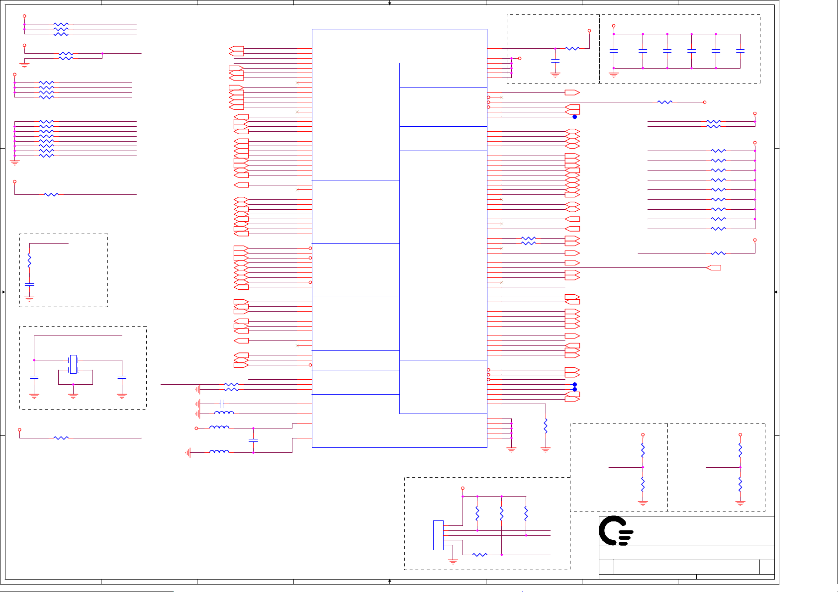
+3.3V_ALW
+3.3V_ALW
+5V_RUN
A A
R189 2.7K 0402R189 2.7K 0402
R187 2.7K 0402R187 2.7K 0402
R181 2.7K 0402R181 2.7K 0402
+3.3V_RUN
B B
1
R151 10K_NCR151 10K_NC
R161 10KR161 10K
R162 10KR162 10K
R169 10KR169 10K
R673 10K_NCR673 10K_NC
R247 4.7KR247 4.7K
R248 4.7KR248 4.7K
R249 4.7KR249 4.7K
R250 4.7KR250 4.7K
R153 100KR153 100K
R154 100KR154 100K
1 2
1 2
1 2
R254 100KR254 100K
R152 100KR152 100K
R672 1K_NCR672 1K_NC
1%
1%
0402
0402
12
CLK_PCI_5025
Place close
R230
R230
to pin 58.
22_NC
22_NC
C228
C228
22P_50V_NC
22P_50V_NC
12
12
12
R385
R385
100K_NC
100K_NC
AC_OFF
SIO_SPI_CS#
DOCK_SMB_ALERT#
CHIPSET_ID0
CLK_KBD
DAT_KBD
CLK_DOCK
DAT_DOCK
DDR_ON
1.2V_ALW_SUS_ON
RUN_ON
SUS_ON
AUX_ON
1.8V_RUN_ON
3.3V_RUN_ON
GPIO4
NB_VCORE_PWRGD
MEC5025_XTAL2
32KHz Clock.
W1
W1
MEC5025_XTAL1
14
10PPM
32.768KHZ
32.768KHZ
23
12.5pF
12.5pF
10PPM
BC_DAT
C C
D D
12
C192
C192
22P_50V
22P_50V
+3.3V_ALW
R253 100KR253 100K
R253 To support SIO BC Bus Speed Lower Speed.
Less than 12MHz
1
12
C206
C206
22P_50V
22P_50V
2
2
CKG_SMBDAT7
CKG_SMBCLK7
1.8V_SUS_PWRGD48
EC_CPU_PROCHOT#10
NB_PWRGD14,20
SUSPWROK19,43
SB_RSMRST#24
CLOCK_ENABLE#7
1.2V_ALW_SUS_ON49
DDR_ON48
ALW_PWRGD_3V_5V47
SIO_SLP_S3#24
SIO_SLP_S5#24
3.3V_RUN_ON42
AUX_ON31
SUS_ON42,43
RUN_ON20,33,42,43
AC_OFF45
NB_VCORE_PWRGD43,49
BC_A_INT#37
BC_A_DAT37
BC_A_CLK37
SIO_A20GATE24
CLK_TP_SIO41
DAT_TP_SIO41
CLK_KBD36
DAT_KBD36
CLK_DOCK36
DAT_DOCK36
8051_RX35
8051_TX35
PLTRST#23,27,38,43
CLK_PCI_502523
LPC_LFRAME#23,30,35,38
LPC_LAD023,30,35,38
LPC_LAD123,30,35,38
LPC_LAD223,30,35,38
LPC_LAD323,30,35,38
CLKRUN#23,32,38
IRQ_SERIRQ23,30,32,38
SB_EC_SPI_CLK25
SB_EC_SPI_DIN25
SB_EC_SPI_DO25
EC_FLASH_SPI_CLK37
EC_FLASH_SPI_DIN37
EC_FLASH_SPI_DO37
SIO_PWRBTN#24
BC_CLK38
38
BC_DAT
BC_INT#38
MEC5025_XTAL2
+3.3V_ALW
R179 0R179 0
R185 10KR185 10K
1 2
4.7U_6.3V_0603
4.7U_6.3V_0603
12
C182
C182
L31
0603 120 200mL31
0603 120 200m
BLM18AG121SN1D
BLM18AG121SN1D
L34
0603 120 200mL34
0603 120 200m
BLM18AG121SN1D
BLM18AG121SN1D
L35
0603 120 200mL35
0603 120 200m
BLM18AG121SN1D
BLM18AG121SN1D
3
CKG_SMBDAT
CKG_SMBCLK
CHIPSET_ID0
GPIO4
1.8V_SUS_PWRGD
EC_CPU_PROCHOT#
NB_PWRGD
SUSPWROK
SB_RSMRST#
CLOCK_ENABLE#
1.2V_ALW_SUS_ON
DDR_ON
ALW_PWRGD_3V_5V
SIO_SLP_S3#
SIO_SLP_S5#
3.3V_RUN_ON
AUX_ON
SUS_ONSUS_ONSUS_ON
RUN_ONRUN_ONRUN_ON
AC_OFF
NB_VCORE_PWRGD
BC_A_INT#
BC_A_DAT
BC_A_CLK
SIO_A20GATE
CLK_TP_SIO
DAT_TP_SIO
CLK_KBD
DAT_KBD
CLK_DOCK
DAT_DOCK
8051_RX
8051_TX
PLTRST#
CLK_PCI_5025
LPC_LFRAME#
LPC_LAD0
LPC_LAD1
LPC_LAD2
LPC_LAD3
CLKRUN#
IRQ_SERIRQ
SB_EC_SPI_CLK
SB_EC_SPI_DIN
SB_EC_SPI_DO
EC_FLASH_SPI_CLK
EC_FLASH_SPI_DIN
EC_FLASH_SPI_DO
SIO_PWRBTN#
BC_CLK
BC_DAT
BC_INT#
MEC5025_XTAL1
5025_XTAL2
12
MEC5025_XOSEL
12
C229
C229
0.1U_16V
0.1U_16V
3
USIO2
USIO2
12
KSO17/GPIOA1/AB1H_DATA
13
KSO16/GPIOA0/AB1H_CLK
14
GPIO5/KSO15
15
GPIO4/KSO14
16
KSO13/GPIO18
17
KSO12/OUT8
18
KSO11/GPIOC7
19
KSO10/GPIOC6
20
KSO9/GPIOC5
23
KSO8/GPIOC4
24
KSO7/GPIO3
25
KSO6/GPIO2
27
KSO5/GPIO1
28
KSO4/GPIO0
29
KSO3/GPIOC3
30
KSO2/GPIOC2
31
KSO1/GPIOC1
32
KSO0/GPIOC0
33
KSI7/GPIO19
34
KSI6/GPIO17
35
KSI5/GPIO10
36
KSI4/GPIO9
37
KSI3/GPIO8
38
KSI2/GPIO7/BC_A_INT#
39
KSI1/GPIO6/BC_A_DAT
40
KSI0/SGPIO30/BC_A_CLK
92
SGPIO34/A20M
50
OUT5/KBRST
75
GPIO94/IMCLK
76
GPIO95/IMDAT
77
KCLK
78
KDAT
79
GPIOA6/EMCLK
80
GPIOA7/EMDAT
81
GPIO20/PS2CLK/8051RX
82
GPIO21/PS2DAT/8051TX
57
LRESET#
58
PCICLK
59
LFRAME#
60
LAD0
PCI POWER/LPC BUS
61
62
63
64
56
102
105
107
103
106
108
109
110
87
86
85
122
124
123
22
125
104
101
PCI POWER/LPC BUS
LAD1
(9)
(9)
LAD2
LAD3
CLKRUN#
SER_IRQ
HSTCLK
HSTDATAIN
HSTDATAOUT
FLCLK
FLDATAIN
FLDATAOUT
GPIO80
GPIO81
BC_CLK
BC_DAT
BC_INT#
XTAL1
XTAL2
XOSEL
VR_CAP
AGND
VCC_PLL
VSS_PLL
MEC5025
MEC5025
LQFP128-16X16-4-JM6
LQFP128-16X16-4-JM6
Rev 080806
Rev 080806
4
MEC5025 EC-08
MEC5025 EC-08
128 PIN VTQFP
128 PIN VTQFP
KEYBOARD/MOUSE
KEYBOARD/MOUSE
(26)
(26)
(10)
(10)
HOST/8051 SPI
HOST/8051 SPI
(8)
(8)
BC
BC
(3)
(3)
CLOCK
CLOCK
(3)
(3)
4
POWER PLANES
POWER PLANES
(6)
(6)
POWER SWITCH
POWER SWITCH
(6)
(6)
ACCESS BUS
ACCESS BUS
(4)
(4)
MISCELLANEOUS
MISCELLANEOUS
(8)
(8)
POWER PLANES
POWER PLANES
(9)
(9)
MLX_53398-0571_NC
MLX_53398-0571_NC
5
POWER_ SW_IN2#/GPIO23
POWER_ SW_IN1#/GPIO22
POWER_ SW_IN0#
BGPO0/GPIOA5
AB1B_CLK/GPIOA4
AB1B_DATA/GPIOA2
GPIO11/AB2_DATA
GPIO12/AB2_CLK
GPIO13/AB1G_DATA
GPIO14/AB1G_CLK
GPIO87/AB1C_DATA
GPIO86/AB1C_CLK
GPIO85/AB1D_DATA
GPIO84/AB1D_CLK
GPIO93/AB1F_DATA
GPIO92/AB1F_CLK
GPIO91/AB1E_DATA
GPIO90/AB1E_CLK
GPIO82/FAN_TACH3
GPIO16/FAN_TACH2
GPIO15/FAN_TACH1
GPIO
GPIO
(36)
(36)
SGPIO45/MSDATA/SPDOUT2
SYSOPT0/SGPIO32/LPC_TX
SYSOPT1/SGPIO33/LPC_RX
OUT11/PWM1
OUT10/PWM0
nEC_SCI/SPDIN2
SGPIO44/MSCLK/SPCLK2
SGPIO46/SPDIN1
SGPIO47/SPDOUT1
SGPIO31/TIN1/SPCLK1
SGPIO36 (SFPI_EN)
GPIO96/TOUT1
GPIOA3/WINDMON
GPIO83/32KHZ_OUT
nRESET_OUT/OUT6
+3.3V_ALW
JDEBUG1
JDEBUG1
5
4
3
2
1
5
Place cap
close to pin
121.
+RTC_CELL_R
121
VCC0
21
VCC1
44
VCC1
65
VCC1
83
VCC1
116
VCC1
ALW_ON
120
ALWON
119
INSTANT_ON_SW#
126
MAIN_PWR_SW#
127
ACAV_IN
128
ACAV_IN
AB1A_CLK
AB1A_DATA
OUT2/PWM3
OUT9/PWM2
SGPIO40
SGPIO41
SGPIO42
SGPIO43
SGPIO35
SGPIO37
OUT7/nSMI
nPWR_LED
nBAT_LED
nFWP
PWRGD
TEST_PIN
VSS
VSS
VSS
VSS
VSS
1 2
R99 0R99 0
1 2
Not Stuff 0 ohm when doing
Flash recovery.
SNIFFER_RTC_GPO
118
LCD_SMBCLK
8
LCD_SMBDAT
7
DOCK_SMB_CLK
6
DOCK_SMB_DAT
5
1.8V_RUN_ON
93
LCDVCC_TST_EN
94
1.2V_SUS_ON
95
CPU_PWRGD_Q
96
PBAT_SMBDAT
111
PBAT_SMBCLK
112
SBAT_DH_SMBDAT
9
SBAT_DH_SMBCLK
10
1.5V_RUN_ON
97
98
THRM_SMBDAT
99
THRM_SMBCLK
100
CPU_VCORE_PWRGD
43
42
FAN1_TACH
41
R208 0R208 0
48
1 2
R202 0R202 0
1 2
47
46
BREATH_LED#
45
SIO_EXT_SCI#
66
PS_ID
55
SIO_RCIN#
54
69
68
DEBUG_ENABLE#
67
HOST_DEBUG_TX
70
HOST_DEBUG_RX
71
CAP_LED#
91
SCRL_LED#
90
NUM_LED#
89
SIO_SPI_CS#
4
LOM_SMB_ALERT#
1
SFPI_EN
2
DOCK_SMB_ALERT#
3
0.9V_DDR_VTT_ON
52
SIO_EXT_SMI#
11
BAT2_LED#
115
BAT1_LED#
114
FWP#
84
GPIOA3_MED5025
73
EC_32KHZ
117
RUNPWROK
49
RESET_OUT#
53
MEC_TEST_PIN
72
113
88
74
51
26
Debug Serial Port
Flash Recovery Port.
R96
R96
R891MR89
10K
10K
1M
1 2
DEBUG_ENABLE#
6
+3.3V_ALW
R94
R94
10K
10K
1 2
8051_RX
8051_TX
6
+RTC_CELL
R193 0R193 0
12
C197
C197
0.1U
0.1U
X5R
X5R
10
10
%
%
±10
±10
0402
0402
R246
R246
1K
1K
5%
5%
0402
0402
1 = Enabled.
0 = Disabled
Flash Recovery.
7
+3.3V_ALW
12
12
12
C251
12
ALW_ON 47
MAIN_PWR_SW#
ACAV_IN 19,46,51
T34
T34
PAD
PAD
LCD_SMBCLK 20
LCD_SMBDAT 20
DOCK_SMB_CLK 36
DOCK_SMB_DAT 36
1.8V_RUN_ON 42
LCDVCC_TST_EN20
1.2V_SUS_ON 26
CPU_PWRGD_Q 23
PBAT_SMBDAT 45
PBAT_SMBCLK 45
SBAT_DH_SMBDAT 45
SBAT_DH_SMBCLK 45
1.5V_RUN_ON 49
THRM_SMBDAT
THRM_SMBCLK 19,46
CPU_VCORE_PWRGD 43,50
FAN1_TACH 19
CPU_VCORE_ENABLE 50
WLAN_3V_ENABLE 35
BREATH_LED# 40
SIO_EXT_SCI# 24
SIO_RCIN# 24
BEEP 28
HOST_DEBUG_TX 35
HOST_DEBUG_RX 35
CAP_LED# 40
SCRL_LED# 40
NUM_LED#
SIO_SPI_CS# 25
LOM_SMB_ALERT# 30
DOCK_SMB_ALERT# 36
0.9V_DDR_VTT_ON 48
SIO_EXT_SMI# 24
BAT2_LED#
BAT1_LED# 40
T35
T35
T33
T33
RUNPWROK 38,43,50
RESET_OUT# 43
C251
10U
10U
10
10
%
%
±20
±20
0805
0805
X5R
X5R
Place these caps close to MEC5025.
R175 100KR175 100K
40
19,46
CPU_VCORE_PWRGD
40
40
PAD
PAD
PAD
PAD
QUANTA
QUANTA
QUANTA
COMPUTER
COMPUTER
Title
Title
Title
Size Document Number Rev
Size Document Number Rev
Size Document Number Rev
Date: Sheet
Date: Sheet
Date: Sheet
COMPUTER
Ultra I/O Controller MEC5025
Ultra I/O Controller MEC5025
Ultra I/O Controller MEC5025
MGD 3A
MGD 3A
MGD 3A
7
C183
C183
0.1U
0.1U
X5R
X5R
10
10
%
%
±10
±10
0402
0402
1 2
DOCK_SMB_CLK
DOCK_SMB_DAT
LCD_SMBCLK
LCD_SMBDAT
PBAT_SMBDAT
PBAT_SMBCLK
SBAT_DH_SMBDAT
SBAT_DH_SMBCLK
THRM_SMBCLK
THRM_SMBDAT
HOST_DEBUG_RX
R163
R163
10K_NC
10K_NC
1 2
R164
R164
10K
10K
1 2
C205
C205
0.1U
0.1U
X5R
X5R
10
10
%
%
±10
±10
0402
0402
Low =
Write Protected.
Flash Write
Protect bottom
4K of internal
bootblock flash.
12
12
C248
C248
0.1U
0.1U
X5R
X5R
10
10
%
%
±10
±10
0402
0402
+RTC_CELL
1 2
1 2
1 2
R195 2.2K
R195 2.2K
FWP#SFPI_EN
8
C250
C250
0.1U
0.1U
X5R
X5R
10
10
%
%
±10
±10
0402
0402
R1598.2K R1598.2K
12
R1608.2K R1608.2K
12
R1578.2K R1578.2K
12
R1588.2K R1588.2K
12
R2142.2K R2142.2K
12
R2032.2K R2032.2K
12
R1562.2K R1562.2K
12
R1552.2K R1552.2K
12
R2374.7K R2374.7K
R2364.7K R2364.7K
R2571M R2571M
12
5%
5%
PS_ID 45
+3.3V_ALW+3.3V_ALW
of
of
of
39 89Thursday, March 01, 2007
39 89Thursday, March 01, 2007
39 89Thursday, March 01, 2007
8
12
C208
C208
0.1U
0.1U
X5R
X5R
10
10
%
%
±10
±10
0402
0402
+5V_ALW
+3.3V_ALW
+3.3V_RUN
12
R252
R252
100K
100K
12
R251
R251
100K_NC
100K_NC
Page 40

A
2
470
470
2
+3.3V_RUN
13
47K
47K
10K
10K
D9
D9
2 1
LTST-C191TBKT
LTST-C191TBKT
+3.3V_SUS
5
U3
U3
NC7SZ04P5X_NL
NC7SZ04P5X_NL
3
SSOP-5
SSOP-5
Q5
Q5
DDTA114YUA-7-F
DDTA114YUA-7-F
3
2
1
4
BREATH_PWRLED
HDD activity LED.
12
R32
R32
10K_NC
10K_NC
5%
5%
0402
+5V_RUN
0402
R26
R26
1 2
R31 10KR31 10K
1 2
4 4
SATA_ACT#25
Blue tooth LED.
BT_ACTIVE35,41
Power & Suspend.
3 3
BREATH_LED#39
2 2
NOTE:LED layout location
Please refer to this location to layout
WI/FI
D6 D5D8 D7 D9
LED_WLAN_OUT#_R
BREATH_PWRLED
R_PIDEACT
1 1
BAT2_LED
BAT1_LED
A
R27 100R27 100
1 2
R22 100R22 100
1 2
R25 100R25 100
1 2
R23 220R23 220
1 2
R24 220R24 220
1 2
RBREATH_PWR_LED
RHDD_LED
RBAT2_LED
RBAT1_LED
2 1
2 1
2 1
3 1
4 2
19-22SURSYGC/S530-A2/TR8
19-22SURSYGC/S530-A2/TR8
B
Symbol:
DDTA114YUA-7-F
OUT(3)
IN(2)
R_PIDEACT 36
Q9
Q9
BSS138_NL
BSS138_NL
GND(1)
Symbol:
BSS138_NL
D(3)
G(2)
D5
D5
LTST-C190GKT-DE
LTST-C190GKT-DE
Green
Green
D6
D6
LTST-C190GKT-DE
LTST-C190GKT-DE
Green
Green
D8
D8
LTST-C190GKT-DE
LTST-C190GKT-DE
Green
Green
D7
D7
B
S(1)
Keyboard Connector
KSO[0..17]37
KSI[0..7]37
POWER_SW#19
NUM_LED#39
CAP_LED#39
SCRL_LED#39
C155 100P_50V_NCC155 100P_50V_NC
1 2
C157 100P_50V_NCC157 100P_50V_NC
1 2
C159 100P_50V_NCC159 100P_50V_NC
1 2
C156 100P_50V_NCC156 100P_50V_NC
1 2
C160 100P_50V_NCC160 100P_50V_NC
1 2
C158 100P_50V_NCC158 100P_50V_NC
1 2
C161 100P_50V_NCC161 100P_50V_NC
1 2
C162 100P_50V_NCC162 100P_50V_NC
1 2
C146 100P_50V_NCC146 100P_50V_NC
1 2
C148 100P_50V_NCC148 100P_50V_NC
1 2
C147 100P_50V_NCC147 100P_50V_NC
1 2
C149 100P_50V_NCC149 100P_50V_NC
1 2
C153 100P_50V_NCC153 100P_50V_NC
1 2
CHECK
MAIN_PWR_SW#39
Battery status.
C
KYBRD_CONN_DETECT#37
KSO[0..17]
KSI[0..7]
POWER_SW#
R127 330R127 330
R128 330R128 330
R129 330R129 330
2
12
12
12
+3.3V_ALW
KSI0 KSO5
KSI1
KSI2
KSI3
KSI4
KSI5
KSI6
KSI7
KSO1
KSO2
KSO3
KSO4
+RTC_CELL
12
R137
R137
100K
100K
R126 10KR126 10K
12
C181
C181
1U
1U
10
10
%
%
±10
±10
0603
0603
X5R
X5R
Q6
Q6
13
DDTA114YUA-7-F
DDTA114YUA-7-F
47K
47K
10K
10K
C
JKB1
JKB1
1
KSO10
KSO11
KSO9
KSO14
KSO13
KSO15
KSO16
KSO12
KSO0
KSO2
KSO1
KSO3
KSO8
KSO6
KSO7
KSO4
KSO5
KSI0
KSI3
KSI1
KSI5
KSI2
KSI4
KSI6
KSI7
R_NUM_LED#
R_CAP_LED#
R_SCRL_LED#
KSO17
C154 100P_50V_NCC154 100P_50V_NC
1 2
C151 100P_50V_NCC151 100P_50V_NC
1 2
C152 100P_50V_NCC152 100P_50V_NC
1 2
C150 100P_50V_NCC150 100P_50V_NC
1 2
C140 100P_50V_NCC140 100P_50V_NC
1 2
C138 100P_50V_NCC138 100P_50V_NC
1 2
C139 100P_50V_NCC139 100P_50V_NC
1 2
C145 100P_50V_NCC145 100P_50V_NC
1 2
C142 100P_50V_NCC142 100P_50V_NC
1 2
C141 100P_50V_NCC141 100P_50V_NC
1 2
C143 100P_50V_NCC143 100P_50V_NC
1 2
C144 100P_50V_NCC144 100P_50V_NC
1 2
C163 100P_50V_NCC163 100P_50V_NC
1 2
Layout Note: C189.1 pad is used
as a Provision For External
Power Cycling, Must place C189
on top to be accessed when
Keyboard is removed.
POWER_SW#
12
12
C189
C189
1U_NC
1U_NC
0603
0603
10 Y5V
10 Y5V
BAT1_LED#39BAT2_LED#39
MH1
2
3
4
5
6
7
8
9
10
11
12
13
14
15
16
17
18
19
20
21
22
23
24
25
26
27
28
29
30
31
32
33
34
MH2
fh28d-34sb-1sh80-34p-l
fh28d-34sb-1sh80-34p-l
12
C170
C170
100P_NC
100P_NC
50
50
%
%
±5
±5
0402
0402
+3.3V_ALW+3.3V_ALW
13
47K
47K
2
10K
10K
KSO6
KSO7
KSO8
KSO9
KSO10
KSO11
KSO12
KSO13KSO0
KSO14
KSO15
KSO16
KSO17
Q7
Q7
DDTA114YUA-7-F
DDTA114YUA-7-F
BAT1_LEDBAT2_LED
D
E
Hall Switch
+3.3V_ALW
Fix Travis issue for
touch pad board
R2101MR210
1M
LID_CL_SIO# LID_CL#
WLAN
LED_WLAN_OUT#35
Title
Title
Title
SWITCH, KEYBOARD & LED
SWITCH, KEYBOARD & LED
SWITCH, KEYBOARD & LED
Size Document Number Rev
Size Document Number Rev
Size Document Number Rev
MGD 2A
MGD 2A
MGD 2A
Date: Sheet
Date: Sheet
D
Date: Sheet
R209 10
R209 10
C212
C212
0.047U
0.047U
25
25
%
%
±10
±10
0402
0402
+3.3V_WLAN
R656
R656
10K
10K
QUANTA
QUANTA
QUANTA
COMPUTER
COMPUTER
COMPUTER
R655
R655
47K
47K
5%0402
5%0402
+3.3V_RUN
2
E
Q8
Q8
MMBT3906
MMBT3906
3 1
LID_CL# 41LID_CL_SIO#38
LED_WLAN_OUT#_R
of
of
of
40 89Thursday, March 01, 2007
40 89Thursday, March 01, 2007
40 89Thursday, March 01, 2007
Page 41

1
A A
B B
2
Lid Switch(Hall)
+3.3V_ALW
+3.3V_RUN
12
C211
C211
0.1U_16V
0.1U_16V
3
LID_CL#40 DAT_TP_SIO 39
+3.3V_ALW
4
Touch Pad
JP1
JP1
1
2
3
4
5
6
7
8
9
10
HT1305F-P2
HT1305F-P2
5
L38 BLM18AG601SN1D
BT_ACTIVE
L38 BLM18AG601SN1D
L37
BLM18AG601SN1D
BLM18AG601SN1D
C237
C237
10P_50V
10P_50V
1 2
BT_ACTIVE 35,40
TP_CLK
TP_DATA
TP_VCC
This circuit is only needed if
the platform has the SNIFFER.
0603
0603
0603L37
0603
+5V_RUN
C236
C236
10P_50V
10P_50V
1 2
6
R560
R560
R561
R561
4.7K
4.7K
4.7K
4.7K
1 2
1 2
C235
C235
10P_50V
10P_50V
1 2
Bluetooth
CLK_TP_SIO 39
C249
C249
10P_50V
10P_50V
1 2
TP_VCC
12
C233
C233
0.1U_16V
0.1U_16V
7
+5V_RUN
R218 0_0805R218 0_0805
1 2
C227
C227
0.047U
0.047U
16
16
X7R
X7R
8
J2
J2
1
GND
3
BT_RADIO_DIS#38 COEX1_BT_ACTIVE 35
PADT1PAD
T1
USBP7+24
C C
BT_RADIO_DIS#
T1
12
C3
0.1U_10VC30.1U_10V
12
C426
C426
100P_50V
100P_50V
3.3V(Logic)
5
Radio Enable/Disable#
7
RSVD
9
USB+
TYC_1566995-1
TYC_1566995-1
Activity LED
COEX2
COEX1
USB-
GND
2
4
6
8
10
R5
10KR510K
1 2
1 2
R4
10KR410K
COEX2_WLAN_ACTIVE
COEX1_BT_ACTIVE
12
C2
33P_50VC233P_50V
COEX2_WLAN_ACTIVE 35
USBP7- 24
EMI solution
please as close as possible to
the connector (J2.1-J2.7) on these traces
+3.3V_RUN
BT_ACTIVE
D D
1
2
COEX2_WLAN_ACTIVE
BT_RADIO_DIS#
COEX1_BT_ACTIVE
T1
3
C743 0.1U
C743 0.1U
12
C744 0.1U
C744 0.1U
12
C745 0.1U
C745 0.1U
12
C746 0.1U
C746 0.1U
12
C747 0.1U
C747 0.1U
12
C748 0.1U
C748 0.1U
12
4
X7R10
X7R10
X7R10
X7R10
X7R10
X7R10
QUANTA
QUANTA
X7R10
X7R10
X7R10
X7R10
X7R10
X7R10
5
6
Title
Title
Title
Size Document Number Rev
Size Document Number Rev
Size Document Number Rev
Date: Sheet
Date: Sheet
Date: Sheet
QUANTA
COMPUTER
COMPUTER
COMPUTER
TOUCH PAD, BULE TOOTH & FIR
TOUCH PAD, BULE TOOTH & FIR
TOUCH PAD, BULE TOOTH & FIR
MGD 2A
MGD 2A
MGD 2A
7
of
of
of
41 89Thursday, March 01, 2007
41 89Thursday, March 01, 2007
41 89Thursday, March 01, 2007
8
Page 42

1
12
PR162
PR162
100K
A A
SUS_ON39,43
SUS_ON
100K
SUS_ON_5V#
34
5
PQ58A
PQ58A
2N7002DW
2N7002DW
12
PR160
PR160
100K
100K
61
2
PQ58B
PQ58B
2N7002DW
2N7002DW
SUS_ENABLE
12
PC155
PC155
4700P_25V
4700P_25V
2
+3.3V_ALW +3.3V_SUS+15V_ALW+3.3V_ALW2
PQ27
PQ27
FDC655BN
FDC655BN
6
5
2
1
3
+5V_ALW +5V_SUS
6
5
2
1
PQ21
PQ21
FDC655BN
FDC655BN
Design current : 338.9mA
Max current : 484.2mA
4
PC71
PC71
12
10U
10U
10
10
%
%
±10
±10
0805
0805
X7R
X7R
EP
EP
4
3
12
Design current : 108mA
Max current : 155mA
PC68
PC68
10U_10V_0805
10U_10V_0805
1 2
PR102
PR102
20K
20K
1 2
3
PR99
PR99
20K
20K
4
+5V_ALW +5V_RUN+15V_ALW+3.3V_ALW2
12
PR161
PR161
100K
100K
RUN_ON_5V#
34
RUN_ON20,33,39,43
5
PQ59A
PQ59A
2N7002DW
2N7002DW
12
PR127
PR127
100K
100K
61
2
PQ59B
PQ59B
12
PC118
2N7002DW
2N7002DW
PC118
4700P_25V
4700P_25V
RUN_ENABLERUN_ENABLE
RUN_ENABLE
PQ16
PQ16
SI4800BDY-T1-E3
SI4800BDY-T1-E3
8
7
6
5
5
Design current : 1888mA
Max current : 2697mA
3
2
1
12
PC62
PC62
10U_10V_0805
4
10U_10V_0805
PR72
PR72
20K
20K
1 2
3
2N7002W-7-F
12
B B
12
PR57
PR57
100K
100K
61
1.8V_RUN_ON39
C C
3.3V_RUN_ON39
D D
1.2V_RUN_ON38
2
PQ13B
PQ13B
2N7002DW
2N7002DW
12
PR86
PR86
100K
100K
61
2
PQ19B
PQ19B
2N7002DW
2N7002DW
12
PR49
PR49
100K
100K
61
2
PQ9B
PQ9B
2N7002DW
2N7002DW
1
+15V_ALW+3.3V_ALW2
12
34
5
+15V_ALW+3.3V_ALW2
3.3V_RUN_ENABLE
34
5
12
1.2V_RUN_ENABLE
34
5
PR56
PR56
100K
100K
1.8V_RUN_ENABLE
PQ13A
PQ13A
2N7002DW
2N7002DW
PR97
PR97
390K
390K
PQ19A
PQ19A
2N7002DW
2N7002DW
PR50
PR50
100K
100K
PQ9A
PQ9A
2N7002DW
2N7002DW
1.8V_RUN_ENABLE 16
+3.3V_ALW +3.3V_RUN
+1.2V_ALW_SUS +1.2V_RUN+15V_ALW+3.3V_ALW2
2
SI4336DY-T1-E3
SI4336DY-T1-E3
8
7
5
6
5
2
1
8
7
6
5
Current = 17
Current = 17
4
12
PC45
PC45
4700P_25V
4700P_25V
PQ14
PQ14
FDC655BN
FDC655BN
4
3
12
PC48
PC48
4700P_25V
4700P_25V
PQ17
PQ17
SI4336DY-T1-E3
SI4336DY-T1-E3
3
2
1
4
PC67
PC67
6800P
6800P
25
25
PQ10
PQ10
1
2
36
+1.8V_RUN+1.8V_SUS
Design current : 308.4mA
Max current : 440.5mA
12
PC49
PC49
10U_10V_0805
10U_10V_0805
Design current : 3201mA
Max current : 4574mA
12
PC52
PC52
10U_10V_0805
10U_10V_0805
12
PC46
PC46
10U_10V_0805
10U_10V_0805
Design current : 2037mA
Max current : 2910mA
PR59
PR59
20K
20K
1 2
PR69
PR69
20K
20K
1 2
RUN_ON_5V#
PR54
PR54
20K
20K
1 2
SUS_ON_5V#
+1.8V_SUS
2
12
PR81
PR81
30_F_NC
30_F_NC
31
PQ20
PQ20
2N7002W-7-F_NC
2N7002W-7-F_NC
+0.9V_DDR_VTT
12
31
2
PR80
PR80
1K_NC
1K_NC
PQ25
PQ25
2N7002W-7-F_NC
2N7002W-7-F_NC
Reserve discharge path
+1.5V_RUN+2.5V_RUN+3.3V_RUN+5V_RUN +1.8V_RUN
2
12
PR83
PR83
1K_NC
1K_NC
31
PQ22
PQ22
2N7002W-7-F_NC
2N7002W-7-F_NC
2
12
PR94
PR94
1K_NC
1K_NC
31
PQ23
PQ23
2N7002W-7-F_NC
2N7002W-7-F_NC
2
12
PR84
PR84
1K_NC
1K_NC
31
PQ24
PQ24
2N7002W-7-F_NC
2N7002W-7-F_NC
2
12
PR92
PR92
1K_NC
1K_NC
31
PQ26
PQ26
2N7002W-7-F_NC
2N7002W-7-F_NC
2
12
PR77
PR77
1K_NC
1K_NC
31
PQ18
PQ18
2N7002W-7-F_NC
2N7002W-7-F_NC
Reserve discharge path
QUANTA
QUANTA
QUANTA
COMPUTER
COMPUTER
Title
Title
Title
Size Document Number Rev
Size Document Number Rev
Size Document Number Rev
Date: Sheet
Date: Sheet
3
4
Date: Sheet
COMPUTER
RUN POWER SW
RUN POWER SW
RUN POWER SW
MGD 2A
MGD 2A
MGD 2A
5
of
of
of
42 89Thursday, March 01, 2007
42 89Thursday, March 01, 2007
42 89Thursday, March 01, 2007
Page 43

1
A A
+5V_RUN +5V_ALW
D14
D14
12
C267
C267
0.1U_16V
0.1U_16V
SDMK0340L-7-F
SDMK0340L-7-F
12
R240
R240
200K
200K
1 2
12
C247
C247
2200P_50V
2200P_50V
1.5V_RUN_PWRGD49
NB_VCORE_PWRGD39,49
R261 10KR261 10K
2
R279 0_NCR279 0_NC
R272 0R272 0
13
Q27
Q27
2
MMBT3906_NL
MMBT3906_NL
1 2
R2422KR242
2K
+1.8V_SUS+1.8V_RUN
1 2
1 2
2
1 3
3
Q24
Q24
MMST3904
MMST3904
4
CPU_VCORE_PWRGD39,50
RESET_OUT#39
12
13
5
+3.3V_ALW
U13D
U13D
11
74VHC08MTCX
74VHC08MTCX
1 2
R276 0R276 0
6
+3.3V_SUS
2
12
R263
R263
100K
100K
31
Q29
Q29
2N7002W-7-F
2N7002W-7-F
SB_PWRGD# 19
SB_PWRGD 24
7
8
Symbol:
2N7002W-7-F
D(3)
G(2)
S(1)
2
2
13
Q31
Q31
MMBT3906_NL
MMBT3906_NL
1 2
13
Q19
Q19
MMBT3906_NL
MMBT3906_NL
1 2
13
Q22
Q22
MMBT3906_NL
MMBT3906_NL
1 2
R244 0R244 0
2
R264
R264
1.2K
1.2K
R112
R112
470
470
R211
R211
1.2K
1.2K
1 2
Q30
Q30
MMST3904
MMST3904
1 3
Keep Away from high speed buses
+3.3V_SUS +3.3V_ALW+3.3V_ALW +3.3V_ALW
R2800R280
1 2
+3.3V_ALW
12
R259
R259
20K
20K
12
C264
C264
0.01U
0.01U
25V
25V
+3.3V_RUN
12
0
R281
R281
20K_NC
20K_NC
12
R282
R282
20K
20K
12
C285
C285
0.01U_16V
0.01U_16V
+3.3V_ALW
5
1 6
C268 0.1U_16VC268 0.1U_16V
1 2
5
U14A
U14A
1 6
74LVC3G14DC
74LVC3G14DC
5V_3V_1.8V_1.2V_RUN_PWRGD38
U11A
U11A
74LVC3G14DC
74LVC3G14DC
5
U14B
U14B
3 4
74LVC3G14DC
74LVC3G14DC
+3.3V_ALW
5
U11B
U11B
3 4
74LVC3G14DC
74LVC3G14DC
C266 0.1U_16VC266 0.1U_16V
1 2
14
U13A
U13A
1
RUN_ON20,33,39,42
SUS_ON39,42
PLTRST#23,27,38,39
2
74VHC08MTCX
74VHC08MTCX
U13C
U13C
10
9
PLTRST#
+3.3V_ALW
3
4
5
8
74VHC08MTCX
74VHC08MTCX
+3.3V_SUS
C286 0.1U_16VC286 0.1U_16V
1 2
5
U15
U15
2
1
+3.3V_ALW
U13B
U13B
4
74AHC1G08GW
74AHC1G08GW
6
74VHC08MTCX
74VHC08MTCX
PLTRST_SYS# 14,22,30,35,49
RUNPWROK 38,39,50
SUSPWROK 19,39
Q18
Q18
MMST3904
MMST3904
2
1 3
Q21
Q21
MMST3904
MMST3904
2
1 3
R245 0R245 0
12
R111
R111
200K
200K
R215
R215
200K
200K
1.2V_ALW_SUS_PWRGD49
R273 10KR273 10K
1 2
12
C269
C269
2200P_50V
2200P_50V
1 2
12
C124
C124
2200P_50V
2200P_50V
1 2
12
C224
C224
2200P_50V
2200P_50V
R115 10KR115 10K
R223 10KR223 10K
+3.3V_ALW
2
D10
D10
D12
D12
12
12
12
R265
R265
200K
200K
SDMK0340L-7-F
SDMK0340L-7-F
12
C126
C126
0.1U_16V
0.1U_16V
+3.3V_RUN +3.3V_ALW
B B
SDMK0340L-7-F
SDMK0340L-7-F
12
C209
C209
0.1U_16V
0.1U_16V
+3.3V_SUS
C C
SDMK0340L-7-F
SDMK0340L-7-F
12
C270
C270
0.1U_16V
0.1U_16V
D15
D15
+5V_SUS +5V_ALW
2
13
Q23
Q23
MMBT3906_NL
MMBT3906_NL
1 2
2
R2582KR258
Q26
Q26
MMST3904
MMST3904
2
2K
1 3
Title
Title
Title
Size Document Number Rev
Size Document Number Rev
Size Document Number Rev
Date: Sheet
Date: Sheet
3
4
5
6
Date: Sheet
QUANTA
QUANTA
QUANTA
COMPUTER
COMPUTER
COMPUTER
System Reset Circuit
System Reset Circuit
System Reset Circuit
MGD 2A
MGD 2A
MGD 2A
7
of
of
of
43 89Thursday, March 01, 2007
43 89Thursday, March 01, 2007
43 89Thursday, March 01, 2007
8
D13
D13
SDMK0340L-7-F
SDMK0340L-7-F
12
C246
D D
C246
0.1U_16V
0.1U_16V
1
R231 10KR231 10K
1 2
12
12
R235
R235
C238
C238
200K
200K
2200P_50V
2200P_50V
Page 44

1
2
3
4
5
6
7
8
Reserved for EMI.MDC
PV7
PV3
PV1
H5
H5
ME_e1
ME_e1
h-c197d63p2
h-c197d63p2
1
A A
H4
4 2
4 2
4 2
ME_d9
ME_d9
ME_a1
ME_a1
ME_a5
ME_a5
H4
35
H7
H7
35
H6
H6
35
1
H-TC276C216D114P2-4
H-TC276C216D114P2-4
1
H-TC276C216D102P2-4
H-TC276C216D102P2-4
1
H10
H10
ME_d1
1
1
B B
1
ME_d1
4 2
H-TC276C216D114P2-4
H-TC276C216D114P2-4
H1
H1
ME_d12
ME_d12
4 2
H-TC276C216D114P2-4
H-TC276C216D114P2-4
ME_a4
ME_a4
4 2
H11
H11
35
35
35
1
H-TC276C216D114P2-4
H-TC276C216D114P2-4
1
H-TC276C216D102P2-4
H-TC276C216D102P2-4
1
4 2
4 2
4 2
ME_d10
ME_d10
ME_a2
ME_a2
ME_d6
ME_d6
H2
H2
H8
H8
H15
H15
H3
H3
ME_d11
1
35
1
35
3
ME_d11
4 2
H-TC276C216D114P2-4
H-TC276C216D114P2-4
ME_a3
ME_a3
4 2
H-TC276C216D102P2-4
H-TC276C216D102P2-4
ME_d7
1
ME_d7
4 2
H12
H12
35
35
H13
H13
3
PV1
PAD195X130_NC
PAD195X130_NC
GND
1
PV8
PV8
PAD195X130_NC
PAD195X130_NC
GND
1
PV15
PV15
PAD195X130_NC
PAD195X130_NC
GND
1
PV2
PV2
PAD195X130_NC
PAD195X130_NC
GND
1
PV9
PV9
PAD195X130_NC
PAD195X130_NC
GND
1
PV16
PV16
PAD195X130_NC
PAD195X130_NC
GND
1
PV3
PAD195X130_NC
PAD195X130_NC
GND
1
PV10
PV10
PAD195X130_NC
PAD195X130_NC
GND
1
HNPTH1
HNPTH1
ME_b1
ME_b1
h-c374d374n
h-c374d374n
PV4
PV4
PAD195X130_NC
PAD195X130_NC
PV11
PV11
PAD195X130_NC
PAD195X130_NC
1
GND
1
GND
1
PV5
PV5
PAD195X130_NC
PAD195X130_NC
GND
1
PV12
PV12
PAD195X130_NC
PAD195X130_NC
GND
1
PV6
PV6
PAD138x98_NC
PAD138x98_NC
GND
1
PV14
PV14
PAD195X130_NC
PAD195X130_NC
GND
1
PV7
PAD138x98_NC
PAD138x98_NC
GND
1
PV13
PV13
PAD195X130_NC
PAD195X130_NC
GND
1
H-TC276C216D114P2-3
H-TC276C216D102P2-4
H-TC276C216D102P2-4
H-TC276C216D102P2-4
H9
4 2
ME_d8
ME_d8
H9
3
C C
D D
1
H-TC276C216D114P2-3
H-TC276C216D114P2-3
1
H-TC276C216D102P2-4
2
H-TC276C216D114P2-3
H-TC276C216D114P2-3
ME_d4
1
ME_d4
4 2
H-C276B372X323D114P2-3
H-C276B372X323D114P2-3
3
H14
H14
3
H-TC276C216D114P2-3
ME_d5
H-C216D114P2-4
H-C216D114P2-4
4
ME_d5
4 2
1
H16
H16
35
QUANTA
QUANTA
QUANTA
COMPUTER
COMPUTER
Title
Title
Title
Size Document Number Rev
Size Document Number Rev
Size Document Number Rev
Date: Sheet
Date: Sheet
5
6
Date: Sheet
COMPUTER
SCREW PAD
SCREW PAD
SCREW PAD
MGD 1A
MGD 1A
MGD 1A
7
of
of
of
44 89Thursday, March 01, 2007
44 89Thursday, March 01, 2007
44 89Thursday, March 01, 2007
8
Page 45
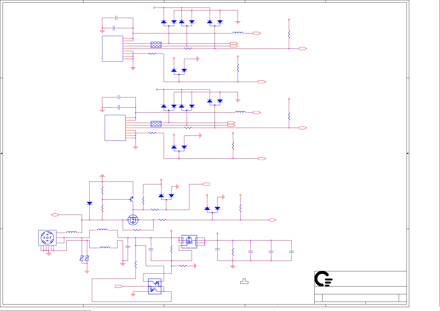
1
JBAT1
JBAT1
A A
Secondary Battery
Connector
BATT_PRES#
BATT_VOLT
TYCO-1566657-1
TYCO-1566657-1
2
PC146 2200P_50VPC146 2200P_50V
12
PC147
PC147
1 2
0.1U_25V_0603
0.1U_25V_0603
1
BATT1+
2
BATT2+
3
SMB_CLK
4
SMB_DAT
5
6
SYSPRES#
7
8
BATT1-
9
BATT2-
+3.3V_ALW
PR148
PR148
4P2R-S-100
4P2R-S-100
2
4
1
1
3
PD7
PD7
DA204U_NC
DA204U_NC
Z4301
Z4302
Z4303
PR51 100_NCPR51 100_NC
1 2
2
1
2
3
+3.3V_ALW
3
PR147 100PR147 100
1 2
2
1
PD4
PD4
DA204U_NC
DA204U_NC
3
PD6
PD6
DA204U_NC
DA204U_NC
3
2
1
PD5
PD5
DA204U_NC
3
DA204U_NC
1 2
FL3
FL3
FBMA-L11-453215-900LMAT_1812
FBMA-L11-453215-900LMAT_1812
SBAT_DH_SMBCLK 39
SBAT_DH_SMBDAT 39
+3.3V_ALW
12
PR53
PR53
10K_NC
10K_NC
SBATT+ 51
NC_SBAT_ALARM#
4
+3.3V_ALW
12
PR52
PR52
10K
10K
5
SBAT_PRES# 38,51
Z4304
Z4305
Z4306
PR182 100_NCPR182 100_NC
13
PQ43
PQ43
2
FDV301N
FDV301N
12
0.1U_25V_NC
0.1U_25V_NC
PR24
PR24
240K_NC
240K_NC
+3.3V_ALW
PD24
PD24
DA204U
DA204U
PR191
PR191
4P2R-S-100
4P2R-S-100
2
4
1 2
12
PR9
PR9
10K
10K
1 2
PR12 100_NCPR12 100_NC
PR17 33PR17 33
1
1 2
1
1
3
+5V_ALW
1
3
1 2
+DC_IN
PC15
PC15
0.47U_25V_0805
0.47U_25V_0805
2
3
PR190 100PR190 100
+3.3V_ALW
1
2
PD1
PD1
DA204U_NC
DA204U_NC
12
PR23
PR23
240K
240K
PR22 47KPR22 47K
1 2
1
1 2
2
3
PQ4
PQ4
1
2
3
Q49_G
2
3
PD20
PD20
DA204U_NC
DA204U_NC
1
PD23
PD23
DA204U
DA204U
PS_ID_DISABLE# 38
+5V_ALW +3.3V_ALW
1
3
FDS6679AZ
FDS6679AZ
8
7
6
54
2
PD22
PD22
DA204U
DA204U
FL4
FL4
FBMA-L11-453215-900LMAT_1812
FBMA-L11-453215-900LMAT_1812
3
+DC_IN_SS
2
PD2
PD2
BAV99W
BAV99W
75
75
SOT-323
SOT-323
EU
EU
130m
130m
PC23
PC23
12
0.01U_25V
0.01U_25V
1 2
+3.3V_ALW
12
12
PBAT_SMBCLK 39
PBAT_SMBDAT 39
PR184
PR184
10K_NC
10K_NC
12
PR18
PR18
2.2K
2.2K
12
PR21
PR21
10K_0603
10K_0603
+3.3V_ALW
PS_ID 39
PC16
PC16
0.1U_25V_0603
0.1U_25V_0603
12
PR187
PR187
10K
10K
12
PBATT+ 51
NC_PBAT_ALARM#
PSID--To Power Management Controller
or EC(ex: Macallan3)
PC18
PC18
0.1U_25V_0603
0.1U_25V_0603
12
PC17
PC17
10U_25V_1206
10U_25V_1206
PBAT_PRES# 38
PC100 2200P_50VPC100 2200P_50V
12
PC99
PC99
1 2
0.1U_25V_0603
0.1U_25V_0603
JBAT2
B B
Primary Battery
Connector
PQ43--Three transistor can be used for
PQ43(pin compatible):FDV301N has low
Vgs_on w/buit-in ESD
protection.MMST3904 BJT works in
reverse conduction mode.
PD14--This diode is no-stuff
populate if PQ22 gets damageed
by ESD.
C C
DOCK_PSID--To Docking
connector(PSID from the dock)
DOCK_PSID36
JDCIN1
JDCIN1
TYC-1770730-1
TYC-1770730-1
98765
D D
DOCK_PSID
PL9
PL9
BLM11B102SPT
BLM11B102SPT
1
1 2
+DCIN_JACK
2
-DCIN_JACK
3
4
RV2
RV2
VZ0603M260AGT_NC
VZ0603M260AGT_NC
SSM24_NC
SSM24_NC
FBMA-L11-453215-900LMAT_1812
FBMA-L11-453215-900LMAT_1812
12
12
JBAT2
BATT1+
BATT2+
SMB_CLK
SMB_DAT
BATT_PRES#
SYSPRES#
BATT_VOLT
BATT1BATT2-
SUYIN_200185MR009S509ZL
SUYIN_200185MR009S509ZL
12
PR131
PR131
15K_F
15K_F
PQ42
PR130
PR130
100K
100K
PQ42
MMST3904
MMST3904
PD14
PD14
12
FL1
FL1
1 2
1 2
FL2
FL2
FBMA-L11-453215-900LMAT_1812
FBMA-L11-453215-900LMAT_1812
RV1
RV1
VZ0603M260AGT_NC
VZ0603M260AGT_NC
1
2
3
4
5
6
7
8
9
2
3
PR132 0_NCPR132 0_NC
1 2
PC21
PC21
12
QUANTA
QUANTA
PQ3
PQ3
34
IMD2A_NC
IMD2A_NC
AC_OFF39
1
2
5
6
2
1
3
3
12
2N7002W-7-F
Title
Title
Title
Size Document Number Rev
Size Document Number Rev
Size Document Number Rev
Date: Sheet
Date: Sheet
4
Date: Sheet
QUANTA
COMPUTER
COMPUTER
COMPUTER
DCIN,BATT CONN.
DCIN,BATT CONN.
DCIN,BATT CONN.
MGD 2A
MGD 2A
MGD 2A
5
of
of
of
45 89Thursday, March 01, 2007
45 89Thursday, March 01, 2007
45 89Thursday, March 01, 2007
Page 46

1
+DC_IN_SS
A A
MAX8731_LDO
12
ACAV_IN19,39,51
B B
C C
D D
ADAPT_TRIP_SEL38
MAX8731_IINP
12
PR106
PR106
8.45K_F
8.45K_F
PR115
PR115
10K_F
10K_F
PR1090PR109
0
PR116
PR116
15.8K_F
15.8K_F
MAX8731_IINP
12
MAX8731_REF
1
GNDA_CHG
THRM_SMBCLK19,39
THRM_SMBDAT19,39
12
PC79
PC79
0.1U_10V
0.1U_10V
PR158
PR158
0_0402
0_0402
12
PC20
PC20
10U_25V_1206
10U_25V_1206
Vin Dectector
High 17.9 V
Low 17.24 V
PR173
PR173
49.9K_F
49.9K_F
PC165 0.01U_25VPC165 0.01U_25V
+5V_ALW
GNDA_CHG
PR166
PR166
10K
10K
0402
0402
EP
EP
1 2
5%
5%
12
PC158
PC158
0.01U_25V
0.01U_25V
PR98
PR98
33.2K_F_NC
33.2K_F_NC
12
12
PR89
PR89
13K_F
13K_F
12
12
PC160 0.1U_10VPC160 0.1U_10V
PC162
PC162
1 2
PR75
PR75
57.6K_F
57.6K_F
1 2
12
1 2
PR76
PR76
105
105
1%
1%
12
1 2
0.01U_25V
0.01U_25V
PC63
PC63
0.01U_25V
0.01U_25V
12
PC50
PC50
0.01U_25V
0.01U_25V
PR177
PR177
365K_F
365K_F
12
12
1U_25V_0805
1U_25V_0805
PC163
PC163
0.01U_25V
0.01U_25V
PC91
PC91
MAX8731_REF
12
PC89
PC89
PR67
PR67
1M_F
1M_F
1 2
12
PC152
PC152
100P_50V
100P_50V
2
GNDA_CHG
22
DCIN
2
ACIN
13
ACOK
11
VDD
10
SCL
9
SDA
14
BATSEL
8
IINP
6
CCV
5
CCI
4
CCS
3
REF
1U_10V_0603
1U_10V_0603
PC149
PC149
100P_50V
100P_50V
1 2
2
PR114
PR114
0.01
0.01
1 2
3
PC166
PC166
0.22U_6.3V_NC
0.22U_6.3V_NC
1
28
GND
CSSP
Adress :
12H
PGND
GNDPAD
DAC
7
12
PC80
PC80
0.1U_10V
0.1U_10V
GNDA_CHG
+5V_ALW
84
3
+
+
2
-
-
2% 1W 3720
2% 1W 3720
4
PR1800PR180
0
27
CSSN
25
BST
MAX8731_LDO
21
LDO
26
VCC
24
DHI
23
LX
20
DLO
19
18
CSIP
17
CSIN
15
FBSA
16
FBSB
29
GND
MAX8731
MAX8731
12
PU7
PU7
12
PC56
PC56
100P_50V
100P_50V
PU4A
PU4A
1
LM393DR2G
LM393DR2G
MAX8731_DHO
MAX8731_DLO
PR112 100PR112 100
12
PC51
PC51
10P_50V_NC
10P_50V_NC
PR120 0_0603PR120 0_0603
1 2
PC90 1U_10V_0603PC90 1U_10V_0603
12
PR175
PR175
33_F_0603
33_F_0603
1 2
1U_10V_0603
1U_10V_0603
PR119 1 0603PR119 1 0603
12
PC57
PC57
100P_50V
100P_50V
12
+SDC_IN
MAX8731_LDO
12
PC164
PC164
12
PC92 220P_50VPC92 220P_50V
+VCHGR
PR71
PR71
100K
100K
1 2
3
21
PD19
PD19
BAT165
BAT165
DSMV
DSMV
EP
EP
0.75
0.75
40
40
PC96
PC96
0.1U_25V_0603
0.1U_25V_0603
12
GNDA_CHG
4
4
PQ36
PQ36
876
SI4800BDY-T1-E3
SI4800BDY-T1-E3
2
351
876
PQ38
PQ38
SI4810BDY-T1-E3
SI4810BDY-T1-E3
2
351
12
PC170
PC170
3.3nF_50V
3.3nF_50V
+VCHGR_B
876
4
2
351
5.6uH_HMU1356-5R6_8.8A
5.6uH_HMU1356-5R6_8.8A
C757
C757
470P_NC
470P_NC
12
PQ34
PQ34
SI4800BDY-T1-E3
SI4800BDY-T1-E3
3
PL6
PL6
4
PC103
PC103
2200P_50V
2200P_50V
12
A00-02
8731AGND
GNDA_CHG
Adapter Trip current PR67 PR72 PR73 PR71
65W 3.17A 57.6K 13K 105 N/A
+3.3V_ALW+5V_ALW
PR70
PR70
100K
100K
1 2
31
PQ57
PQ57
2
2N7002W-7-F
2N7002W-7-F
1 2
3
R311
R311
1K_NC
1K_NC
ADAPT_OC 38
4
+CHGR_L
5
6
12
PC102
PC102
0.1U_25V_0603
0.1U_25V_0603
PR125
PR125
0.01
0.01
1 2
3
PR1240PR124
0
1 2
1 2
±10
±10
X5R
X5R
+
+
-
-
12
PC107
PC107
10U_25V_1206
10U_25V_1206
+VCHGR
PC110
PC110
10U
10U
X5R
X5R
1206
1206
25
25
5
A00-02
5
PC112
PC112
10U
10U
X5R
X5R
1206
1206
25
25
+SDC_IN
+5V_ALW
46 89Thursday, March 01, 2007
46 89Thursday, March 01, 2007
46 89Thursday, March 01, 2007
PD13
PD13
1SS355
1SS355
PR126
PR126
1K
1K
1%
1%
0603
0603
PC176
PC176
10U
10U
X5R
X5R
1206
1206
25
25
TABLE 3, PIN NAME DIFFERENCES
PIN MAXIM INTRSIL
1 GND NC
3 REF VREF
4 CCS ICOMP
5 CCI NC
6 CCV VCOMP
7 DAC NC
8 IINP ICM
11 VDD VDDSMB
14 BATSEL NC
15 FBSA VFB
16 FBSB NC
17 CSIN CSON
18 CSIP CSOP
20 DLO LGATE
21 LDO VDDP
23 LX PHASE
24 DHI UGATE
25 BST BOOT
12
12
12
PC105
PC105
2200P_50V_NC
2200P_50V_NC
2% 1W 3720
2% 1W 3720
4
PC84
PC84
%
%
0.22U_NC
0.22U_NC
6.3
6.3
PU4B
PU4B
7
LM393DR2G
LM393DR2G
Title
Title
Title
Size Document Number Rev
Size Document Number Rev
Size Document Number Rev
Date: Sheet
Date: Sheet
Date: Sheet
PC171
PC171
PC104
PC104
Battery Charger
Battery Charger
Battery Charger
MGD 3A
MGD 3A
MGD 3A
10U_25V_1206
10U_25V_1206
0.1U_25V_0603_NC
0.1U_25V_0603_NC
12
PC111
PC111
PC108
PC108
10U
10U
0.1U_25V_0603
0.1U_25V_0603
X5R
X5R
1206
1206
25
25
Ref DES MAXIM INTRSIL
PR66 8.45K_F 16K_F
PC52 0.01uf No STUFF
PC43 0.1U_10V No STUFF
PC47 1U_10V_0603 No STUFF
PR53 365K_F 215K_F
PR63 0 10
PR52 0 10
PC42 No STUFF 0.22uf
PC24 No STUFF 0.22uf
PC45 0.01uf No STUFF
PC48 0.1uf_10V No STUFF
PC38 220pf_50V No STUFF
PD15 CH501H-40PT No STUFF
PC36 3.3nf_50V No STUFF
PR61 1_0603 0_0603
PR65 100 0
PR64 4.7K 4.7K
PC44 0.01uf 0.01uf
PC46 0.01uf 0.01uf
QUANTA
QUANTA
QUANTA
COMPUTER
COMPUTER
COMPUTER
A00-11
PR168
PR168
2.37K
2.37K
1206
1206
1%
1%
of
of
of
Page 47
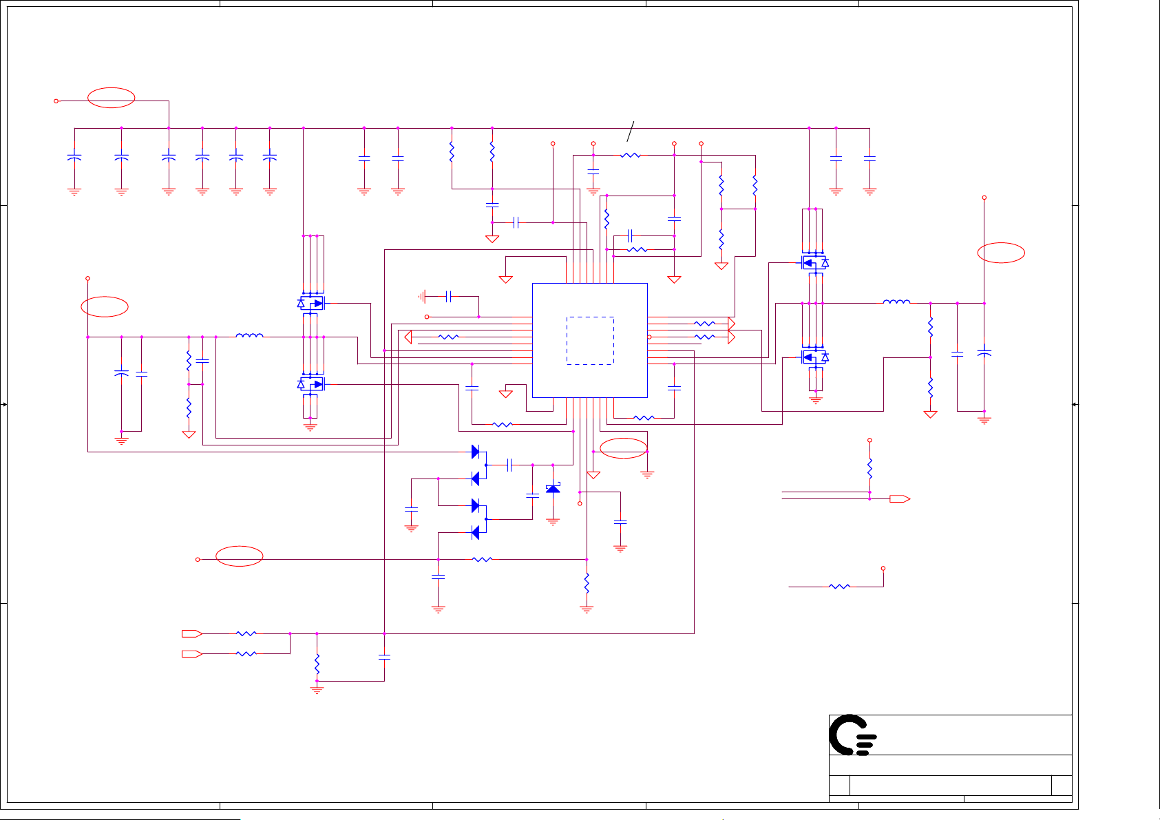
5
4
3
2
1
DC/DC +3V_ALW/+5V_ALW/+5V_ALW2 /+15V_ALW
+PWR_SRC
D D
5 Volt +/- 5%
TDC=6A
max current=8.55A
OCP point is 10.5A
C C
B B
A00-02
12
+
+
PC178
PC178
100U_25V
100U_25V
+5V_ALW
A00-02
PC172
PC172
330U_6.3V_ESR25
330U_6.3V_ESR25
12
+
+
PC179
PC179
100U_25V
100U_25V
+
+
PC116
PC116
0.1U_10V
0.1U_10V
1 2
+15V_ALW
PC101
PC101
12
12
+
+
10U_25V_1206
10U_25V_1206
2.2UH +-20%13A(SIQH125A-2R2-R)
2.2UH +-20%13A(SIQH125A-2R2-R)
PR171
PR171
0_0603_NC
0_0603_NC
PR176
PR176
0_0603
0_0603
GNDA_3V5V
1 2
1 2
1 2
PC106
PC106
+
+
10U_25V_1206
10U_25V_1206
1 2
PC87
PC87
1000P_50V_0402_NC
1000P_50V_0402_NC
A00-02
PC117
PC117
12
+
+
10U_25V_1206
10U_25V_1206
PL7
PL7
PC173
PC173
12
+
+
10U_25V_1206
10U_25V_1206
PQ37
PQ37
FDS8880
FDS8880
PQ39
PQ39
FDS6676AS
FDS6676AS
876
351
876
351
2
2
Place these CAPs
close to FETs
1 2
+5V_ALW_UGATE
4
+5V_ALW_PHASE
+5V_ALW_LGATE
4
PC109
PC109
0.1U_50V_0603
0.1U_50V_0603
+5V_ALW
GNDA_3V5V
0.1U_25V_0603
0.1U_25V_0603
No Install for ISL6236
Install 10 ohm for MAX8778
+5V_ALW2
PC82
PC82
0.1U_25V_0603
0.1U_25V_0603
C758 0.1UC758 0.1U
GNDA_3V5V
9
10
11
12
13
14
15
16
PR183
PR183
0_0603
0_0603
PC169
PC169
0.1U_25V_0603
0.1U_25V_0603
12
PC95
PC95
1 2
0.1U_25V_0603
0.1U_25V_0603
+3.3V_ALW2
BYP
OUT1
FB1
ILIM1
POK1
EN1
UGATE1
PHASE1
GNDPAD
33
BAT165
BAT165
2 1
6
8
7
5
VIN
LDO
VREF3
LDOREFIN
PU9
PU9
ISL6236
ISL6236
QFN32-5x5-5-33P
QFN32-5x5-5-33P
BOOT117LGATE118PVCC19SECFB20GND21PGND22LGATE223BOOT2
GNDA_3V5V
PD21
PD21
DSMV
DSMV
EP
EP
0.75
0.75
40
40
+5V_ALW2
12
PC159
PC159
4.7U
4.7U
10
10
0805
0805
3
4
EN_LDO
PR188
PR188
39K_F
39K_F
10_0603_NC
10_0603_NC
PR165
PR165
0_0402_NC
0_0402_NC
1 2
1
REF
TON2VCC
24
A00-02
PC115
PC115
12
PR107
PR107
PR108
PR108
0_0805
0_0805
0_0805
0_0805
1 2
GNDA_3V5V
0402
0402
10
10
X7R
X7R
%
%
±10
±10
1 2
PD12
PD12
1
2
BAT54SLT1G
BAT54SLT1G
PD11
PD11
1
2
BAT54SLT1G
BAT54SLT1G
1 2
1 2
12
GNDA_3V5V
1 2
3
3
2200P_50V
2200P_50V
PC85
PC85
0.1U_NC
0.1U_NC
PR179 143K 1%PR179 143K 1%
POK1 POK2
PC167
PC167
0.1U_25V_0603
0.1U_25V_0603
PC93
PC93
0.1U_25V_0603
0.1U_25V_0603
1 2
PR189 200K_FPR189 200K_F
PC98
PC98
1 2
+VCC_+3P3V_+5V
PR163
PR163
PC88
PC88
0.1U_10V_0402
0.1U_10V_0402
1 2
PR164
PR164
REFIN2
ILIM2
OUT2
SKIP#
POK2
EN2
UGATE2
PHASE2
PR185
PR185
0_0603
0_0603
1 2
12
PC94
PC94
1U_10V_0603
1U_10V_0603
12
PC161
PC161
12
12
0_NC
0_NC
GNDA_3V5V
32
PR172 100K 1%PR172 100K 1%
31
30
SKIP#
29
28
27
26
25
PC168
PC168
0.1U_25V_0603
0.1U_25V_0603
1 2
+3.3V_ALW_LGATE
5V_3V_REF
0_0402_NC
0_0402_NC
1U_10V_0603
1U_10V_0603
0_0402_NC
0_0402_NC
PR192 0PR192 0
+3.3V_ALW_UGATE
PR169
PR169
1 2
PR167
PR167
1 2
GNDA_3V5V
GNDA_3V5V
GNDA_3V5V
PR170
PR170
0_0402
0_0402
1 2
Place these CAPs
close to FETs
PC113
PC113
12
PC114
PC114
2200P_50V
2200P_50V
1 2
0.1U_50V_0603
0.1U_50V_0603
876
PQ41
PQ41
FDS8880
4
4
POK2
POK1
FDS8880
2
351
+3.3V_ALW_PHASE
876
PQ40
PQ40
FDS6676AS
FDS6676AS
2
351
Ton:OUT1/OUT2 Switching Frequency
GND: 400kHz/500kHz
4.7uH(HMP1340-4R7)
4.7uH(HMP1340-4R7)
+3.3V_ALW
12
PR117
PR117
200K_F
200K_F
PL8
PL8
GNDA_3V5V
LDO = 5V (LDOREFIN = GND)
REFIN2 = VCC: 3.3V Fixed
+VCC_+3P3V_+5V
PR193
PR193
SKIP#
0_NC
0_NC
3.3 Volt +/- 5%
TDC=4.2A
max current=5.95A
OCP point is 11.47A
+3.3V_ALW
A00-02
PR178
PR178
PC175
PC175
0
0
0603
0603
PR174
PR174
0_NC
0_NC
0603
0603
ALW_PWRGD_3V_5V 39
1 2
0.1U_10V
0.1U_10V
+
+
PC174
PC174
330U_6.3V_ESR25
330U_6.3V_ESR25
ALW_ON39
THERM_STP#19
A A
5
PR110 1K_FPR110 1K_F
PR111 0PR111 0
12
12
12
PR113
PR113
200K
200K
4
PC83
PC83
0.1U_NC
0.1U_NC
0402
0402
10
10
X7R
X7R
%
%
±10
±10
QUANTA
QUANTA
QUANTA
COMPUTER
COMPUTER
Title
Title
Title
Size Document Number Rev
Size Document Number Rev
Size Document Number Rev
Date: Sheet
Date: Sheet
3
2
Date: Sheet
COMPUTER
3VALW,5V,3V, Power On
3VALW,5V,3V, Power On
3VALW,5V,3V, Power On
MGD 3A
MGD 3A
MGD 3A
1
of
of
of
47 89Thursday, March 01, 2007
47 89Thursday, March 01, 2007
47 89Thursday, March 01, 2007
Page 48

A
+PWR_SRC
A00-04
1 1
12
PC76
PC76
10U
10U
25
PC157
PC157
+
+
330U_2.5V_ESR15
330U_2.5V_ESR15
88550 AVDD
25
1206
1206
X6S
X6S
±10
±10
design current=9.24A for+1.8V_SUS
max current=13.2A for+1.8V_SUS
OCP point :16.56A
+1.8V_SUS
2 2
A00-04
12
PC78
PC78
0.1U_10V
0.1U_10V
12
PC77
PC77
10U
10U
25
25
1206
1206
X6S
X6S
±10
%
%
PR159 0PR159 0
±10
PC156
PC156
+
+
330U_2.5V_ESR15
330U_2.5V_ESR15
27.4K_F_0603_NC
27.4K_F_0603_NC
1 2
B
12
PC75
PC75
2200P
2200P
50
50
±10
±10
%
%
0402
0402
X7R
X7R
%
%
PL5
12
12
PR82
PR82
17.4K_F_0603_NC
17.4K_F_0603_NC
GND_DDR
PL5
PC66
PC66
1000P_50V_NC
1000P_50V_NC
1 2
1.5UH20%17A(SIQH126-1R5PF)LF
1.5UH20%17A(SIQH126-1R5PF)LF
PR90
PR90
PC74
PC74
0.1U_25V_0603
0.1U_25V_0603
1 2
12
9
9
C759
C759
0.01U
0.01U
GND_DDR
876
351
876
351
2
2
PQ29
PQ29
FDS6298
FDS6298
PC70 0.22U_10V_0603PC70 0.22U_10V_0603
4
PQ28
PQ28
FDS6299S
FDS6299S
4
Freq=300K
0.22U_6.3V
0.22U_6.3V
21
PD9
PD9
BAT165
BAT165
DSMV
DSMV
EP
EP
0.75
0.75
+5V_SUS
PC72
PC72
4.7U_10V_0805
4.7U_10V_0805
PR103 0_0603PR103 0_0603
88550_DH
+1.8VSUSP_L
88550_DL
PR101 0_NCPR101 0_NC
12
12
PC69
PC69
C
1 2
20
18
19
21
23
16
15
12
PR95
PR95
100K_F
100K_F
1
3
PR96
PR96
63.4K
63.4K
1%
1%
BST
DH
LX
DL
PGND1
OUT
FB
TON
REF
PR105 10_F_0603PR105 10_F_0603
PR1000PR100
0
1 2
22
2
VDD
OVP/UVP
PU6
PU6
MAX8632ETI+
MAX8632ETI+
QFN28-5x5-5-29P
QFN28-5x5-5-29P
TP0
SKIP
ILIM
4
25
28
12
PR104
PR104
0_NC
0_NC
1 2
26
AVDD
POK1
POK2
SHDN
STBY
VTTI
REFIN
PGND2
GNDPAD
VTTS
VTTR
GND
24
88550 AVDD
VIN
VTT
SS
8
12
17
5
6
27
7
13
14
11
29
12
9
10
+3.3V_SUS
PC73
PC73
1 2
1U_10V_0603
1U_10V_0603
GND_DDR
+PWR_SRC
A00-17
0.9V_DDR_VTT_PWRGD
PR73 0PR73 0
1 2
PR74 20_F_0603PR74 20_F_0603
1 2
12
PC64
PC64
0.1U_10V
0.1U_10V
GND_DDR
PC60
PC60
1 2
1U_10V_0603
1U_10V_0603
GND_DDR
PC65
PC65
1000P_50V
1000P_50V
A00-04
12
PR93
PR93
100K
100K
PR79 0_NCPR79 0_NC
1 2
+1.8V_SUS
+V_DDR_VREF
12
PR88
PR88
100K_NC
100K_NC
12
PC150
PC150
0.1U_10V
0.1U_10V
D
1.8V_SUS_PWRGD 39
12
PC59
PC59
10U_6.3V_0805
10U_6.3V_0805
12
PC151
PC151
10U_6.3V_0805
10U_6.3V_0805
0.9V_DDR_VTT_ON 39
+1.8V_SUS
Design current 1.925A for+0.9V_DDR_VTTP
12
PC153
PC153
10U_6.3V_0805
10U_6.3V_0805
E
DDR_ON 39
Max current 2.75A for +0.9V_DDR_VTTP
A00-04
12
PC154
PC154
10U_6.3V_0805_NC
10U_6.3V_0805_NC
+0.9V_DDR_VTT
GND_DDRGND_DDR
3 3
4 4
A
B
C
GND_DDR
QUANTA
QUANTA
QUANTA
COMPUTER
COMPUTER
Title
Title
Title
Size Document Number Rev
Size Document Number Rev
Size Document Number Rev
Date: Sheet
Date: Sheet
D
Date: Sheet
COMPUTER
1.8V_SUS,0.9V_VTT
1.8V_SUS,0.9V_VTT
1.8V_SUS,0.9V_VTT
MGD 2A
MGD 2A
MGD 2A
2005/4/21
E
of
of
of
48 89
48 89
48 89
Page 49

5
4
3
2
1
+PWR_SRC
D D
1.2 Volt +/- 5%
design current=2.3A
max current 3.3A
OCP point: 3.75A
+1.2V_ALW_SUS
A00-05
C C
B B
5V_3V_REF
12
PR85
PR85
49.9K_F
49.9K_F
12
PR78
PR78
150K_F
150K_F
A A
+1.8V_SUS
1.5V_RUN_PWRGD43
A00-05
PC125
PC125
220U_2.5V_ESR15
220U_2.5V_ESR15
+
+
1.5V_RUN_ON39
12
PC13
PC13
10U_25V_1206
10U_25V_1206
+
+
add a note to PC3:
populate PC3 with
0.01U_16V with
ISL6236; populate
PC3 with 1uF_16V
with Max8778
SI4800BDY-T1-E3
SI4800BDY-T1-E3
PL2
PL2
4.7uH (MPL73_4R7)
4.7uH (MPL73_4R7)
PC22
PC22
0.1U_10V
0.1U_10V
1 2
PR68 0_0603PR68 0_0603
1 2
12
5
SI4810BDY-T1-E3
SI4810BDY-T1-E3
PR4
PR4
17.8K
17.8K
1%
1%
0603
0603
PR10
PR10
24.9K
24.9K
1%
1%
0603
0603
GNDA_1P25V_GPU_CORE
PC58
PC58
1U_10V_0603_NC
1U_10V_0603_NC
PC6
PC6
1000P_50V_NC
1000P_50V_NC
1 2
DC_1+1.5V_RUN_PWR_SRC
+3.3V_ALW
PR91
PR91
100K_NC
100K_NC
12
PC14
PC14
10U_25V_1206
10U_25V_1206
+
+
1.2V_ALW_SUS_ON39
12
12
PC54
PC54
1U_0603_10V
1U_0603_10V
PC123
PC123
1 2
PQ46
PQ46
PQ45
PQ45
10
2
5
7
4
PC124
PC124
0.1U_25V_0603
0.1U_25V_0603
12
2200P_50V
2200P_50V
876
2
351
876
2
351
PU5
PU5
IN
VCC
MAX8794
MAX8794
PGOOD
SHDN
REFIN
12
PR129
PR129
0_0805
0_0805
12
PC2
PC2
0.1U_0603_25V
0.1U_0603_25V
PC120
PC120
1000P_50V_0402_NC
1000P_50V_0402_NC
GNDA_1P25V_GPU_CORE
PR13 143K 1%PR13 143K 1%
1.2V_UGATE1
4
1.2V_PHASE1
1.2V_LGATE1
4
9
OUT
6
OUTS
8
PGND
3
AGND
1
REFOUT
BP
11
GND_8794
12
PC53
PC53
1U_0603_10V
1U_0603_10V
12
PR128
PR128
0_0805
0_0805
+3.3V_RTC_LDO
12
GNDA_1P25V_GPU_CORE
PC3
PC3
0.01U_16V
0.01U_16V
1 2
GNDA_1P25V_GPU_CORE
8
9
BYP
10
OUT1
11
FB1
12
ILIM1
QFN32-5x5-5-33P
PR14 0PR14 0
1 2
PC8
PC8
0.1U_25V_0603
0.1U_25V_0603
1 2
1 2
+5V_ALW
12
PC12
PC12
1U_10V_0603
1U_10V_0603
PR16
PR16
0_0603
0_0603
13
14
15
16
GNDA_1P25V_GPU_CORE
PR19
PR19
10_0603_NC
10_0603_NC
QFN32-5x5-5-33P
POK1
EN1
UGATE1
PHASE1
GNDPAD
33
+5V_VCC4
12
12
PC119
PC119
1U_10V_0603
1U_10V_0603
GNDA_1P25V_GPU_CORE
A00-05
GNDA_1P25V_GPU_CORE
PGND and GND should be
tied together at one point near the GND Pin
1.5V_RUN +/- 5%
Design current 262.5 mA
Peak Current 375 mA
12
4
PC61
PC61
10U_4V_0805
10U_4V_0805
12
PC55
PC55
10U_4V_0805
10U_4V_0805
+5V_VCC4
12
PR30PR3
0
1 2
PR2
PR2
0_NC
0_NC
6
1
7
3
5
4
VIN
LDO
TON2VCC
VREF3
EN_LDO
LDOREFIN
PU1
PU1
ISL6236
ISL6236
BOOT117LGATE118PVCC19SECFB20GND21PGND22LGATE223BOOT2
24
PR20 0_0603PR20 0_0603
GNDA_1P25V_GPU_CORE
1.5V_OUT
PC4
PC4
0.1U
0.1U
PR1
PR1
25
1 2
32
REFIN2
31
ILIM2
30
OUT2
29
SKIP#
28
POK2
27
EN2
26
25
PC9
PC9
0.1U_25V_0603
0.1U_25V_0603
N_Vcore_LGATE2
PR87 0_0603PR87 0_0603
25
12
3
0_NC
0_NC
GNDA_1P25V_GPU_CORE
REF
UGATE2
PHASE2
1 2
1 2
GNDA_1P25V_GPU_CORE
PR11 158K 1%PR11 158K 1%
PR15 0PR15 0
1 2
Power Sequencing, Vcore Regulator
+1.5V_RUN
PC7
PR5
PR5
80.6K
80.6K
1%
1%
PR6
PR6
121K
121K
1%
1%
PC7
1000P_50V
1000P_50V
1 2
GNDA_1P25V_GPU_CORE
NB_VCORE_RUN_ON 38
Power Sequencing
NB_VCORE_PWRGD 39,43
1.2V_ALW_SUS_PWRGD 43
N_Vcore_UGATE2
N_Vcore_PHASE2
N_Vcore_REFIN2
4
4
PR7 243K
PR7 243K
PQ1A
PQ1A
2N7002DW
2N7002DW
2
1%
1%
12
PC10
PC10
+
+
10U_25V_1206
10U_25V_1206
PQ44
PQ44
876
SI4800BDY-T1-E3
SI4800BDY-T1-E3
2
351
PL1
PL1
3.3U_MPL73-3R3 6A_20%
3.3U_MPL73-3R3 6A_20%
876
PQ2
PQ2
SI4810BDY-T1-E3
SI4810BDY-T1-E3
2
351
34
5
12
PC5
PC5
0.01U_25V_NC
0.01U_25V_NC
GNDA_1P25V_GPU_CORE
Title
Title
Title
Size Document Number Rev
Size Document Number Rev
Size Document Number Rev
Date: Sheet
Date: Sheet
Date: Sheet
12
PC122
PC122
PC121
0.1U_25V_0603
0.1U_25V_0603
1 2
PC121
12
2200P_50V
2200P_50V
PC11
PC11
+
+
10U_25V_1206
10U_25V_1206
Layout Same Location
L81
L81
FBM-11-201209-221-A30T
FBM-11-201209-221-A30T
+1.2V/1.0V_VCCP
+1.2V/1.0V_VCCP
1 2
PC27
PC27
0.1U_10V
0.1U_10V
A00-13
L82
L82
FBM-11-201209-221-A30T
FBM-11-201209-221-A30T
PC24
PC24
PC19
PC19
220U_2.5V_ESR15
220U_2.5V_ESR15
220U_2.5V_ESR15_NC
220U_2.5V_ESR15_NC
+
+
+
+
+NB_VCORE
GPU_CORE +/- 5%
Design current: 2.5A
Maximum Current:3.5A
OCP point: 4.2A
PR8 10K_FPR8 10K_F
12
PLTRST_SYS# 14,22,30,35,43
61
2
PQ1B
PQ1B
2N7002DW
2N7002DW
QUANTA
QUANTA
QUANTA
COMPUTER
COMPUTER
COMPUTER
1.2VCPP,VCC_NB,1.5V_RUN,1,2V_ALW
1.2VCPP,VCC_NB,1.5V_RUN,1,2V_ALW
1.2VCPP,VCC_NB,1.5V_RUN,1,2V_ALW
MGD 3A
MGD 3A
MGD 3A
NB_VCORE_CNTRL 14
49 89Thursday, March 01, 2007
49 89Thursday, March 01, 2007
49 89Thursday, March 01, 2007
1
of
of
of
Page 50

A
+5V_RUN
1 1
CPU_VCORE_PWRGD39,43
VID010
VID110
VID210
VID310
VID410
VID510
PR28 100K_NCPR28 100K_NC
3
1
PR141
PR141
100K
100K
8774VCC
+VCC_CORE
GND_VHCORE
PQ50
PQ50
AP2N7002K
AP2N7002K
12
2
PR27 0_NCPR27 0_NC
1 2
1 2
PR136
PR136
100K
100K
+5V_RUN
CPU_VR_PROCHOT#38
+5V_RUN
PR140
PR140
100K
100K
2
PQ49
PQ49
2
UMT3904
UMT3904
1 3
PR55 100K_NCPR55 100K_NC
12
PWR_MON19
RUNPWROK38,39,43
CPU_VCORE_ENABLE39
2 2
PR138 is reserved for AMD
Earthshine load tool during
vaildation and testing
3 3
4 4
+1.8V_SUS
PR138
PR138
10K_NC
10K_NC
CPU_PSI#10
PR137 2.2KPR137 2.2K
B
PR145
PR145
100K
100K
GND_VHCORE
PR135 0PR135 0
1 2
PR134 0_NCPR134 0_NC
1 2
PR39 20KPR39 20K
1 2
PR139 71.5K_FPR139 71.5K_F
PC132 470P_50VPC132 470P_50V
1 2
1 2
PC133
PC133
0.1U_25V_0603
0.1U_25V_0603
PR143
PR143
169K_F
169K_F
31
PQ52
PQ52
2N7002W-7-F
2N7002W-7-F
GND_VHCORE
PR30 10KPR30 10K
PC131
PC131
0.1U
0.1U
%
%
±10
±10
PR32 13K_FPR32 13K_F
16
16
8774VCC
8774VCC
PC137
PC137
2.2U
2.2U
10
10
X7R
X7R
0603
0603
GND_VHCORE
1 2
PC36 470P_50VPC36 470P_50V
8774REF
A00-16
PR142
PR142
26.1K
26.1K
1%
1%
8774OFS
8774OFS8774OFS
12
PC130
PC130
470P_50V_0603_NC
470P_50V_0603_NC
GND_VHCORE
12
12
GND_VHCORE
19
VCC
37
TWO-PH
17
PHASEG
1
PWRGD
31
D0
32
D1
33
D2
34
D3
35
D4
36
D5
40
IC
38
SHDN
39
SKIP
9
CCI
6
TIME
8
CCV
10
REF
2
OFS
4
VRHOT
3
POUT
5
THRM
MAX8774
MAX8774
PU8
PU8
QFN40-6x6-5-41P
QFN40-6x6-5-41P
PR26
PR26
NTC 10K_6-B4.25K
NTC 10K_6-B4.25K
PR40 10_FPR40 10_F
12
BST1
PGND1
CSP1
CSN1
GNDS
BST2
CSP2
CSN2
PGND2
GNDPAD
25
TON
DH1
LX1
DL1
GND
FB
DH2
LX2
DL2
VDD
PR31 200K_FPR31 200K_F
7
8774DH1
29
PR29 2.4
PR29 2.4
30
8774LX1
28
8774DL1
26
27
18
8774CSP1
16
8774CSN1
15
11
12
8774DH2
21
PR36 2.4
PR36 2.4
20
8774LX2
22
24
8774CSP2
13
8774CSN2
14
23
41
CH501H-40PT_NC
CH501H-40PT_NC
1 2
PGND1
A00-06
GND_VHCORE
12
PC136
PC136
1000P_50V
1000P_50V
GND_VHCORE
CH501H-40PT_NC
CH501H-40PT_NC
8774DL2
GND_VHCORE
PD15
PD15
PR38 10PR38 10
PD3
PD3
+5V_ALW
1 2
21
0805
0805
1 2
PR144 1.5K_F_0603_NCPR144 1.5K_F_0603_NC
12
+5V_RUN
21
0805
0805
1 2
C
+5V_RUN
PR41
PR41
0_0603_NC
0_0603_NC
1 2
PC31
PC31
4.7U
4.7U
25
25
X6S
X6S
0805
0805
4
PQ48
PQ48
SI4386DY-T1-E3
SI4386DY-T1-E3
PC30
PC30
0.22U_16V_0603
0.22U_16V_0603
4
PQ5
PQ5
FDS7088SN3
FDS7088SN3
PR37 2.49K_F_0603PR37 2.49K_F_0603
12
PR4310PR43
10
4
PQ54
PQ54
SI4386DY-T1-E3
SI4386DY-T1-E3
PC34
PC34
0.22U_16V_0603
0.22U_16V_0603
4
PQ7
PQ7
FDS7088SN3
FDS7088SN3
RDS(ON)=4.9m ohm
PR42
PR42
0_0603
0_0603
876
9
876
9
4
PQ51
PQ51
SI4386DY-T1-E3
SI4386DY-T1-E3
2
351
2
351
876
9
876
9
4
2
351
2
351
PQ6
PQ6
FDS7088SN3
FDS7088SN3
RDS(ON)=4.9m ohm
PR146 10_FPR146 10_F
PC39
PC39
1000P
1000P
50
50
876
876
2
351
876
9
9
4
PQ53
PQ53
SI4386DY-T1-E3
SI4386DY-T1-E3
2
351
9
876
9
4
2
351
2
351
12
PC25
PC25
1500P_50V_0805_NC
1500P_50V_0805_NC
PC138
PC138
1000P_50V_NC
1000P_50V_NC
1 2
PQ8
PQ8
FDS7088SN3
FDS7088SN3
12
PC43
PC43
1500P_50V_0805_NC
1500P_50V_0805_NC
12
PR25
PR25
2.4_1206_NC
2.4_1206_NC
12
PC28
PC28
1500P_50V_0805_NC
1500P_50V_0805_NC
PR35
PR35
8774CSP1
GND_VHCORE
12
12
12
PC44
PC44
1500P_50V_0805_NC
1500P_50V_0805_NC
8774CSP2
D
PC128
PC128
0.1U
0.1U
50
50
0603
0603
X7R
X7R
PC29, PC41 and PC42 are Sanyo 25CE100LS caps,
and that they should be placed close to the input power of
+VCC_CORE to reduce cap singing
PL3
PL3
0.45U(25A,+-20%,MPC1040LR45)
0.45U(25A,+-20%,MPC1040LR45)
12
3
4
2K
2K
PR34 4.02K 1%PR34 4.02K 1%
1%
1%
12
PC37 0.22U_16V_0603PC37 0.22U_16V_0603
8774CSN1
PC38
PC38
1000P_NC
1000P_NC
±5
±5
%
%
CC0402
CC0402
+VCC_CORE
12
PR44 10PR44 10
CPU_VDD_RUN_FB_L 10
PC142
PC142
0.1U
0.1U
50
PR45
PR45
2.4_1206_NC
2.4_1206_NC
PR46
PR46
2K
2K
1%
1%
PC33
PC33
1000P_NC
1000P_NC
±5
±5
GND_VHCORE
50
0603
0603
X7R
X7R
PL4
PL4
0.45U(25A,+-20%,MPC1040LR45)
0.45U(25A,+-20%,MPC1040LR45)
12
3
4
PR47 4.02K 1%PR47 4.02K 1%
12
PC35 0.22U_16V_0603PC35 0.22U_16V_0603
8774CSN2
%
%
GND_VHCORE
D4
D1
D2
D3
D5
0
00
0
0
0
0 1.5250V
0
0
0
1
0
0
0
0
0
0
1
0
0
1
0
0
0
0
0
0
0
1
0
0
1
0
1
0
0
1
0
1
0
10
0
0
0
01
0
1
0
1
0
0
0
1
0
1
0
1
0
0
0
1
1
101
1
0
0
1
1
0
1
0
0
0
1
1
1
0
0
0
1
0
0
0
0
1
0
0
1
0
1
0
0
0
1
1
0
0
0
1
1
1
1
0
0
0
1
1 1.0000V
1
0
0
0
1
1
0
1
000
1
0
1
1
0
0
0
1
1
0
1
0
1
1
1
0
1
0
1
1
1
0
0
1
0
1
1
0
1
1
1
1 0.8000V
0
1
1
1
1
PC26
PC26
12
PC127
PC127
10U
10U
25
25
2200P_50V
2200P_50V
1206
1206
X6S
X6S
10K_0603_ERTJ1VR103J
10K_0603_ERTJ1VR103J
PR33
PR33
PC40
PC40
1000P_NC
1000P_NC
%
%
±5
±5
CC0402
CC0402
GND_VHCORE
12
PC141
PC141
2200P_50V
2200P_50V
PC32
PC32
1000P_NC
1000P_NC
%
%
±5
±5
Output
D0
1.5500V
0
1
0
1.5000V
1
1.4750V
0
1.4500V
1.4250V
1
1.4000V
0
1.3750V
1
1.3500V
0
1.3250V
1.3000V
0
1.2750V
100
0
1.2500V
1.2250V
1.2000V
0
1
1.1750V
00
1.1500V
1
1.1250V
0
1.1000V
1.0750V
1
1.0500V
0
1.0250V
1
0
0.9750V
1
0
0.9500V
1
0.9250V
0
0.9000V
0.8750V
1
0
0.8500V
0.8250V
1
0
1
0.7750V
12
+
+
PC135
PC135
330U_2V_ESR6
330U_2V_ESR6
CPU_VDD_RUN_FB_H 10
PC140
PC140
10U
10U
25
25
1206
1206
X6S
X6S
PR48
PR48
10K_0603_ERTJ1VR103J
10K_0603_ERTJ1VR103J
D3
D4
D5
0
1
0
0
1
0
0
0
1
0
0
1
0
01
0
1
0
0
0
1
1
0
0
1
1
1
1
0
1
1
0
1
1
0
1
1
0
1
1
0
1
0
1
0
1
1
10
1
0
1
1
0
0
1
1
1
0
1
0
1
1
0
1
1
0
1
1
1
0
1
1
1
1
1
1
1
1
1
1
1
1
1
1
1
1
1
1
1
1
1
1
1
1
PC129
PC129
10U
10U
25
25
1206
1206
X6S
X6S
D2
0
0
0
0
1
1
1
0
0
0
0
1
1
1
1
0
0
0
1
1
1
1
0
0
0
0
1
1
1
1
+PWR_SRC
12
+
+
PC29
PC29
100U_25V
100U_25V
PC134
PC134
12
330U_2V_ESR6
330U_2V_ESR6
+
+
PC139
PC139
10U
10U
25
25
1206
1206
X6S
X6S
12
PC143
PC143
+
+
330U_2V_ESR6
330U_2V_ESR6
D0
Output
D1
0
0
0.7625V
0
1
0.7500V
1
0.7375V
0
11
1
0.7250V
0
0
0.7125V
0.7000V
1
0
1
0
0.6875V
1
1
0.6750V
0.6625V
00
0
0.6500V
1
0
0.6375V
0
1
1
0.6250V
1
0
0
0.6125V
0
1
0.6000V
0.5875V
1
0
1
0.5750V
1
0
0
0.5625V
0
0.5500V
1
1
0.5375V
0
1
1
0.5250V
0
0.5125V
0
0
1
0.5000V
0
0.4875V
1
0.4750V
1
1
0
0
0.4625V
0.4500V
0
1
0.4375V
0
1
1
0.4250V
1
0
010.4125V
1
0.4000V
0
0.3875V
1
0
1
0.3750V
1
12
+
+
PC41
PC41
100U_25V_NC
100U_25V_NC
12
PC144
PC144
+
+
330U_2V_ESR6
330U_2V_ESR6
+PWR_SRC
12
+
+
PC42
PC42
100U_25V
100U_25V
E
A00-06
+VCC_CORE
Peak current maximum
is on 35A
+VCC_CORE
QUANTA
QUANTA
QUANTA
COMPUTER
COMPUTER
COMPUTER
Title
Title
Title
VHCORE (MAX8774)
VHCORE (MAX8774)
VHCORE (MAX8774)
Size Document Number Rev
Size Document Number Rev
Size Document Number Rev
MGD 3A
MGD 3A
MGD 3A
Date: Sheet
Date: Sheet
A
B
C
D
Date: Sheet
E
50 89Thursday, March 01, 2007
50 89Thursday, March 01, 2007
50 89Thursday, March 01, 2007
of
of
of
Page 51

Symbol:
2N7002W-7-F
1
2
3
4
5
D(3)
G(2)
A A
B B
C C
D D
S(1)
PQ31
PQ31
SI4835BDY
SI4835BDY
8
7
1
6
+SDC_IN
PR186
PR186
10K
10K
PR121
31
PQ61
PQ61
1 2
PR65
PR65
47K_F
47K_F
2N7002W-7-F
2N7002W-7-F
PR58
PR58
470K
470K
2
2N7002W-7-F
1
2
3
PQ15
PQ15
2
2N7002W-7-F
PQ30
SI4835BDY
SI4835BDY
4
PR66
PR66
10K
10K
31
8
7
6
5
12
PQ11A
PQ11A
FDS4935BZ
FDS4935BZ
CHG_SBAT
+VCHGR
CHG_SBAT_N
31
PQ55
PQ55
PC47
PC47
2N7002W-7-F
2N7002W-7-F
2
4
PQ56
PQ56
2
2N7002W-7-F
2N7002W-7-F
PQ33
PQ33
2
2N7002W-7-F
2N7002W-7-F
3 1
CHG_PBAT_N
+VCHGR
SBATT+
12
31
CHG_SBATT38
CHG_PBATT38
0.1U_25V_0603_NC
0.1U_25V_0603_NC
+3.3V_ALW
5
PU3
PU3
PBAT_DSCHG38
SBAT_PRES#38,45
2
1
1
TC7SET32FU(T5L,F,T)
TC7SET32FU(T5L,F,T)
3
PR154
PR154
42.2K_F_0603
42.2K_F_0603
PR155 10K_FPR155 10K_F
1 2
PR153
PR153
32.4K_F
32.4K_F
1 2
PR150
PR150
10K
10K
PR122
PR122
10K
10K
17
8
2
PR149 100KPR149 100K
12
PC145 0.1U_25V_0603PC145 0.1U_25V_0603
CHG_SBATT_N
CHG_PBATT_N
PC97 0.1U_25V_0603PC97 0.1U_25V_0603
12
PR123 100KPR123 100K PQ30
4
5
3
CHG_PBAT
PQ35
PQ35
SI4835BDY
SI4835BDY
3
2
2
CHG_PBAT
2
1
PBATT+
PR61
PR61
100
100
PBATT+_393VCC
84
PU2A
PU2A
+
+
-
-
LM393DR2G
LM393DR2G
SOIC8-6-1_27
SOIC8-6-1_27
+3.3V_ALW
PR157
PR157
147K_F
147K_F
PC148 0.1U_25V_0603PC148 0.1U_25V_0603
PD18
PD18
3
1
1PS70SB45
1PS70SB45
SOT-323
SOT-323
Lead-Free
Lead-Free
6
7
8
PR156
PR156
100K
100K
12
40
40
FDS4935BZ
FDS4935BZ
3 5
3
2
1
2
1
PQ11B
PQ11B
4
4
PQ32
PQ32
SI4835BDY
SI4835BDY
1 2
PR63
PR63
47K_F
47K_F
6
5
6
7
8
ACAV_IN19,39,46
PR62
PR62
470K
470K
5
+
+
6
-
-
SOIC8-6-1_27
SOIC8-6-1_27
LM393DR2G
LM393DR2G
PR64 100KPR64 100K
3
PBATT+45
PU2B
PU2B
7
+3.3V_ALW
PR181 100K_NCPR181 100K_NC
PR60
PR60
470K
470K
31
PQ62
PQ62
2
2N7002W-7-F
2N7002W-7-F
SBAT_C
SBATT+45
2
1
1PS70SB45
1PS70SB45
PD17
PD17
2
1
1PS70SB45
1PS70SB45
SOT-323
SOT-323
40
40
Lead-Free
Lead-Free
4
PR121
10K
10K
PD16
PD16
SBAT_G
3
SOT-323
SOT-323
40
40
Lead-Free
Lead-Free
PBAT_C
PBAT_G
3
Title
Title
Title
Battery Selector
Battery Selector
Battery Selector
Size Document Number Rev
Size Document Number Rev
Size Document Number Rev
MGD 2A
MGD 2A
MGD 2A
Date: Sheet
Date: Sheet
Date: Sheet
2
5
3
4
PD8
PD8
ES3BB-13-F
ES3BB-13-F
PQ12
PQ12
SI4835BDY
SI4835BDY
8
7
1
6
2
5
3
4
PR151
PR151
33K
33K
PD10
PD10
ES3BB-13-F
ES3BB-13-F
PQ60
PQ60
SI4835BDY
SI4835BDY
8
7
1
6
2
5
3
4
PR152
PR152
33K
33K
QUANTA
QUANTA
QUANTA
COMPUTER
COMPUTER
COMPUTER
12
PR118
PR118
100K
100K
+PWR_SRC
PC86
PC86
2200P_50V
2200P_50V
5
12
PC81
PC81
0.1U_25V_0603
0.1U_25V_0603
+PWR_SRC
of
of
of
51 89Thursday, March 01, 2007
51 89Thursday, March 01, 2007
51 89Thursday, March 01, 2007
Page 52

5
4
3
2
1
Reserved for EMI.
Stitching caps
12
C319
C319
0.1U/10V_NC
0.1U/10V_NC
+1.05V_VCCP
12
C320
C320
0.1U/10V_NC
0.1U/10V_NC
1 2
C322
C322
0.1U
0.1U
X7R
X7R
0402
0402
+/-10%
+/-10%
10
10
+1.05V_VCCP
D D
C C
12
C356
C356
0.1U/25V_NC
0.1U/25V_NC
+1.5V_RUN +1.8V_SUS
12
C317
C317
0.1U/10V_NC
0.1U/10V_NC
+1.05V_VCCP +3.3V_RUN
12
+1.5V_RUN
C318
C318
0.1U/10V_NC
0.1U/10V_NC
+1.5V_RUN+PWR_SRC
12
C328
C328
0.1U/10V_NC
0.1U/10V_NC
+1.8V_SUS+1.5V_RUN +3.3V_RUN
+1.05V_VCCP
B B
A A
QUANTA
QUANTA
QUANTA
COMPUTER
COMPUTER
Title
Title
Title
Size Document Number Rev
Size Document Number Rev
Size Document Number Rev
Date: Sheet
Date: Sheet
5
4
3
2
Date: Sheet
COMPUTER
EMI CAP
EMI CAP
EMI CAP
MGD 1A
MGD 1A
MGD 1A
1
of
of
of
52 89Thursday, March 01, 2007
52 89Thursday, March 01, 2007
52 89Thursday, March 01, 2007
Page 53

5
4
3
2
1
+0.9V_DDR_VTT
+1.2V_ALW_SUS
+0.9V_MEM_VTT
+1.2V_SUS
+1.2V_LOM +1.2V_AVDDL
D D
+1.2V_GPHY_PLLVDD
+1.2V_PCIE_PLLVDD
+1.2V_PCIE_SDSVDD
+1.2V_RUN
+1.2V_VDDA12
+1.2V_PCIE_VDDR
+1.2V_PCIE_PVDD
+1.2V_PLLVDD_SATA
+1.2V_AVDD_SATA
C C
+1.2V_AVDDCK
+1.2V_VDDA12 +1.2V_PLLVDD12
+1.2V_VDDPLL
+1.2V_IOPLLVDD
+1.8V_RUN
+1.8V_AVDDQ
+1.8V_PLLVDD
+3.3V_ALW +3.3V_LAN
+3.3V_WLAN
+3.3V_SIO_VDDA
+3.3V_RUN +3.3V_CLK
+3VS_CLK_VDD48
+3VS_CLK_VDDREF
+3VS_CLK_VDDA
+3.3V_AVDD
+LVDDR33A
+3.3V_VDDR
+3.3V_LDOIN
+LCDVDD
+3.3V_XTLVDD_SATA
+3.3V_AVDD_HWM
+3.3V_AVDDCK
+3.3V_CB_VCCA
+3.3V_SUS +3VSUS_THRM
+1.8V_HTPVDD
+1.8V_RUN_AVDDDI
+LPVDD
B B
+LVDDR18D
+1.8V_VDD
+5V_ALW +5V_ALW_USB
+5V_ALW_USB +USB_SIDE_PWR
+1.8V_VDD_MEM
+1.8V_IOPLLVDD
+5V_RUN +CRT_VCC
+1.8V_MEM_VDDQ
+1.8V_SUS
+0.9V_CPU_M_VREF_SUS
+2.5V_LOM +2.5V_AVDD
+3.3V_ACDD_USB
+3.3V_AVDDC
+3.3V_ALW_R
+USB_BACK_PWR
+5V_RUN_SYNC
+5V_SPK_AMP
TP_VCC
+2.5V_XTALVDD
A A
2.5V_BIASVDD
+2.5V_RUN +2.5V_CPU_VDDA_RUN
QUANTA
QUANTA
QUANTA
COMPUTER
COMPUTER
COMPUTER
Title
Title
Title
Power Rail for system
Power Rail for system
Power Rail for system
Size Document Number Rev
Size Document Number Rev
Size Document Number Rev
MGD 1A
MGD 1A
MGD 1A
Date: Sheet
Date: Sheet
5
4
3
2
Date: Sheet
1
of
of
of
53 89Thursday, March 01, 2007
53 89Thursday, March 01, 2007
53 89Thursday, March 01, 2007
Page 54

5
4
3
2
1
072806 PG.7
Add C722 0.47uF cap close to U1 on +3.3V_CLK_VDDA to GND after the ferrite for decoupling
072806 PG.7
Add C723 0.47uF cap close to U1 on +3VS_CLK_VDD48 to GND after the ferrite for decoupling
D D
072806 PG.7
Add C724 0.47uF cap close to U1 on +3VS_CLK_VDDREF to GND after the ferrite for decoupling
072006 PG.7
Changed MINI2CLK_REQ# to route to CLKREQB# pin 32 of the clock chip, and MINI1CLK_REQ# routed to CLKREQC#.
072006 PG.7
All components of CLK_PCIE_MINI1 can be removed, including the series resistors R14, R15, R21, and R20.
No connect pins 47 and 46 of the clock chip, U1.
072206 PG.7
Remove the series resistor R27 on the CLK_SMCARD_48M, because this signal is not used.
C C
No connect pin 7 of the clock chip, U1.
072206 PG.7
Add a 10pF NC cap to ground on the following clocks for WWAN antennae tuning:
CLK_SB_48M
CLK_SIO_14M
CLK_NB_14M
CLK_SB_14M
CLK_HTREF_66M
072206 PG.9
Because need to avoid DDR2 signals crossing, DIMM should be placed, routed and added notes as below:
B B
DIMMA = Far = Bottom
DIMMB = Near = Top
072206 PG.9
Add note.
072206 PG.10
Change C32 from 470pF to 220pF
(This is the cap that is between H_THERMDC and H_THERMDA)
072206 PG.10
Rmoved C284/100uF form page 19 to close L5 on page 10.
A A
071206 PG.10
Change C28 from 3900pF to 3300pF
(This cap is on +2.5V_CPU_VDDA_RUN)
5
4
Title
Title
Title
Size Document Number Rev
Size Document Number Rev
Size Document Number Rev
Date: Sheet
Date: Sheet
3
2
Date: Sheet
QUANTA
QUANTA
QUANTA
COMPUTER
COMPUTER
COMPUTER
Changed List P01
Changed List P01
Changed List P01
MGD 1A
MGD 1A
MGD 1A
54 89Thursday, March 01, 2007
54 89Thursday, March 01, 2007
54 89Thursday, March 01, 2007
of
of
1
of
Page 55

5
4
3
2
1
072206 PG.10
Populate Q3 and R90
(These parts populate the CPU_EC_PROCHOT# circuit)
072206 PG.10
Change R91 from the +3.3V_RUN rail to the +3.3V_SUS rail
D D
(R91 is a pull-up on CPU_EC_PROCHOT#)
072206 PG.13
Delete R107 and R109.(Include NOTE)
(These pins are NC for RS690T, and are only used on the RS485 that will not be used.)
072806 PG.14
Added R641/33 and C726/22pF for AC term.And add note :RC closely clock
pin for length: 50 mils
072206 PG.14
C C
Delete L11.
(L11 is a pop option to connect +LVDDR18A on the RS485 to +1.8V_RUN, but the RS690T uses +3.3V_RUN)
Change symbol pin name from LVDDR18A_ to LVDDR33A_
Change signal pin name from +LVDDR18A to +LVDDR33A
072206 PG.14,25,30,35
Populate R118
No pop R299-R301
Pop R387 (LOM control)
Pop R466 (WLAN)
(The plan is to use PLTRST_SYS# to reset PCIE devices at first, and not use the GPIOs)
B B
072206 PG.14
Delete R120, and R122.
(These resistors are pull-ups on LCD_DDCCLK and LCD_DDCDAT, which are duplicates of R137, and R142)
072206 PG.14
Change C113 from 470pF to 220pF
(This cap is between NB_THERMDA, and NB_THERMDC)
072206 PG.14
No Connect R140, R139, and C115
A A
(These parts are on the NC RS690T flash)
QUANTA
QUANTA
QUANTA
COMPUTER
COMPUTER
Title
Title
Title
Size Document Number Rev
Size Document Number Rev
Size Document Number Rev
Date: Sheet
Date: Sheet
5
4
3
2
Date: Sheet
COMPUTER
Changed List P02
Changed List P02
Changed List P02
MGD 1A
MGD 1A
MGD 1A
55 89Thursday, March 01, 2007
55 89Thursday, March 01, 2007
55 89Thursday, March 01, 2007
of
of
1
of
Page 56

5
4
3
2
1
072206 PG.14
No Connect R127, and C114.
(These parts are on the BMREQ# circuit.)
072406 PG.16
D D
Added Resister/68ohm/0402/5% between MEM_CLKP and MEM_CLKN, and note place res to colse to U5.
072806 PG.17
Added Note for decoupling (total of 8 caps) for JDIM1, the note is "Place C185~C189 and C195~C198
close to JDIM1". Changed to "no pop" on C244-C251 with same as Beck for reserve stitching function
between +1.8V_SUS and 0.9V_DDR_VTT.And change C185~189 to 0.1uF for memory power decoupling.
072806 PG.17
Added Note for decoupling (total of 8 caps) for JDIM2, the note is "Place C190~C194 and C199~C202
close to JDIM2". Changed to "no pop" on C252-C259 with same as Beck for reserve stitching function
between +1.8V_SUS and 0.9V_DDR_VTT.And change C190~194 to 0.1uF for memory power decoupling.
C C
072406 PG.18
No pop C244…C259.
(The 16 caps from +1.8V_SUS to +0.9V_DDR_VTT are only populated if needed.)
072406 PG.18
Delete C241, C242, C243.
(These are 3 additional +1.8V to +0.9V caps. The 16 caps C244...C259 are enough, and these 3 can be deleted.)
072806 PG.19
Change R166 and R168 to be pulled up by +3.3V_SUS, not +5V_SUS
(R166 and R168 are on the VCP2 circuit)
B B
072806 PG.19
Change the Q13 pin 2 connection from 5V_CAL_SIO2# to 5V_CAL_SIO1# that connects to pin 14 on the ECE4001.
(Q13 is on the VCP2 circuit)
072806 PG.19
Populate the VCP 2 circuit for thermals.
The circuit includes: R166, C266, Q13, and R168.
A A
QUANTA
QUANTA
QUANTA
COMPUTER
COMPUTER
Title
Title
Title
Size Document Number Rev
Size Document Number Rev
Size Document Number Rev
Date: Sheet
Date: Sheet
5
4
3
2
Date: Sheet
COMPUTER
Changed List P03
Changed List P03
Changed List P03
MGD 1A
MGD 1A
MGD 1A
56 89Thursday, March 01, 2007
56 89Thursday, March 01, 2007
56 89Thursday, March 01, 2007
of
of
1
of
Page 57

5
4
3
2
1
072806 PG.19
Change R171 from 10k NC to 47k NC
(R171 is the pull-up on THERM_STP# to +RTC_CELL)
072806 PG.19
Add R634 7.5k resistor to pulled up to +3.3V_SUS on 2.5V_RUN_ON , and not routed to the EC.
D D
072806 PG.19
Change C280 to 10uF caps and add C727 10uF cap.
(These are decoupling caps on +3.3V_RUN, and +2.5V_RUN for the +2.5V_RUN LDO circuit)
072806 PG.19
Add a RB751 diode in series between R170 pin 1, and J1 pin 2 of the fan connector.
072806 PG.19
No Pop C270
(C270 is a 100pF cap on FAN1_TACH)
C C
072806 PG.20
Change R195 from 100k to 200k to match Becks.
072806 PG.20
Add 0.1uF cap to pin 1 of Q17, LCDVDD switch, to match Becks.
072806 PG.20
Add diode or circuit to pin 2 of Q20. For EC control of power to panel, add wire ORed configuration with
GPU and EC OR control of LCDVCC power switch. Add a NoPop 0 ohm bypass resistor for diode in GPU
control path so that this change can be backed out. Connect the EC control for LCDVCC to
MEC5025 - GPIO12/AB2A_CLK. Signal name is LCDVCC_TST_EN
B B
072706 PG.20
Change Q20 form DDTC124EUA-7-F to DTC124EUA_7-F. Because DDTC124EUA-7-F(Q20) is not available in Quanta
warehouse, but we had DTC124EUAT-106(Q20) which feature is same as DDTC124EUA-7-F, and the vendor
is ROHM who is in Dell PSL.
073006 PG.23
Add R637 0ohm series resistor at pin C1, X2 input of SB, of U10.
Series resistor needed for tuning crystal circuit
073006 PG.23
Remove R246. This signal is NoPop so resistor is not needed.
A A
073006 PG.23
Connect PCI_REQ4# and PCI_GNT4# to test point and remove off page arrow symbol.
5
4
3
2
Title
Title
Title
Size Document Number Rev
Size Document Number Rev
Size Document Number Rev
Date: Sheet
Date: Sheet
Date: Sheet
QUANTA
QUANTA
QUANTA
COMPUTER
COMPUTER
COMPUTER
Changed List P04
Changed List P04
Changed List P04
MGD 1A
MGD 1A
MGD 1A
57 89Thursday, March 01, 2007
57 89Thursday, March 01, 2007
57 89Thursday, March 01, 2007
of
of
1
of
Page 58

5
4
3
2
1
073006 PG.24
No AC Term at load on CLK_SB_14M. Add AC term(R633,C710) close to load (~50 mils from clock pin).
073006 PG.24
No AC Term at load on CLK_SB_48M. Add AC term(R632,C709) close to load (~50 mils from clock pin).
D D
073006 PG.24
Add one C439 0.1uF cap from +3.3V_AVDD_USB to GND for USB PWR decoupling. NoPop this capacitor.
073006 PG.24
Add FET isoation circuits on page 35 for SMBUS, signal MEM_SDATA and MEM_SCLK, to WLAN with pull ups
connected to WLAN power plane. Pull up resitor should be connected to +3.3V_WLAN
073006 PG.24
Change pull up resistor to NoPop for R263, R267, R268, R269, R264, R259 and R260 same as Becks
073006 PG.24
C C
Change SHUTDOWN#/GPIO5 pull up power plane, R259, from 3.3V_SUS to 3.3V_RUN, same as Becks
073006 PG.23
Add pad for cap C728 from PCI_CLK1 to GND for AC term. Place AC term close to load (~50 mils from clock pin).
073006 PG.23
Add pad for cap C725 on PCI_CLK0 to GND for AC term. Place AC term close to load (~50 mils from clock pin).
073006 PG.23
Add pad for cap C714 on CLK_PCI_PCCARD to GND for AC term. Place AC term close to load (~50 mils from clock pin).
073006 PG.23
B B
Add pad for cap C713 on CLK_PCI_DOCK to GND for AC term. Place AC term close to load (~50 mils from clock pin).
073006 PG.25
Add three 0.1uF caps(C441,C442,C443) from +1.2V_AVDD_SATA to GND for Serial ATA Power decoupling.
NoPop these capacitors.
073006 PG.25
Add one 0.1uF cap(C586) from +1.2V_PLLVDD_SATA to GND for Serial ATA Power decoupling
NoPop capacitor
073006 PG.26
No EMI decoupling for +1.2V_RUN. Add two 0.1uF(C731,C732) caps from Power nets to GND.
NoPop these capacitors
A A
QUANTA
QUANTA
QUANTA
COMPUTER
COMPUTER
Title
Title
Title
Size Document Number Rev
Size Document Number Rev
Size Document Number Rev
Date: Sheet
Date: Sheet
5
4
3
2
Date: Sheet
COMPUTER
Changed List P05
Changed List P05
Changed List P05
MGD 1A
MGD 1A
MGD 1A
58 89Thursday, March 01, 2007
58 89Thursday, March 01, 2007
58 89Thursday, March 01, 2007
of
of
1
of
Page 59

5
4
3
2
1
073006 PG.26
No EMI decoupling for +3.3V_RUN. Add two 0.1uF(C733,C734) caps from Power nets to GND.
NoPop these capacitors.
073006 PG.26
Add two 0.1uF cap(C735,C736) on +3.3V_AWL_R to GND for decoupling
D D
073006 PG.30
Add one more 0.1uF cap(C737) on +1.2V_AVDDL to GND for decoupling if space allows
NoPop capacitor
073006 PG.30
Add one more 0.1uF(C738) cap on +2.5V_AVDD to GND for decoupling if space allows.
NoPop capacitor.
073006 PG.30
Connect LOM_GPIO0 to USIO2 pin 1 (SGPIO35) -- This LOM_GPIO0 is SMBALERT for SMBUS. Check SGPIOx of EC (USIO2)
connections to be consistent with Dell M08 design.
C C
073006 PG.31
Add another 0.1uF(C721) capacitor in paralled with C510 to match Becks
073006 PG.31
Remove comment regarding "centerTap" voltage. Remove entire comment since only Broadcom LOMs are supported.
073006 PG.33
Delete C566 and C560.
(These caps are the 150uF no connect caps for USB side and back power. Only one 150uF cap is needed for each
rail, and there is not any need to have an option for two per rail.)
B B
073006 PG.33
No pop serial port capacitors same as Becks. C546, C552, C548, C550, C554-C557.
073006 PG.35
Add one 0.1uF cap(C560) on +1.5V_RUN to GND close to J9 for decoupling
NoPop capacitor
073006 PG.35
Populate R466 so that the WLAN is reset w/ PLTRST_SYS#
A A
QUANTA
QUANTA
QUANTA
COMPUTER
COMPUTER
Title
Title
Title
Size Document Number Rev
Size Document Number Rev
Size Document Number Rev
Date: Sheet
Date: Sheet
5
4
3
2
Date: Sheet
COMPUTER
Changed List P06
Changed List P06
Changed List P06
MGD 1A
MGD 1A
MGD 1A
59 89Thursday, March 01, 2007
59 89Thursday, March 01, 2007
59 89Thursday, March 01, 2007
of
of
1
of
Page 60

5
4
3
2
1
073006 PG.37
Pin 31 GPIO_4 on the 1077 should connect to KYBRD_CONN_DETECT# w/ a 100k pull-up to +3.3V_ALW,
and route to pin 1 of the keyboard connector. This signal is currently connected to
the south bridge.That connection at the SB and the pull up resistor should be removed.
Delect signal connection to Soutbridge
Delete R309.
D D
073006 PG.37
Change R489 from 0 Ohms to 1k
(R489 is a pull-down on the test pin on the ECE1077)
073006 PG.14
add a 0 ohm series resistor on LCD_DDCDAT between R142 pin 2 and Q8 pin 1. Pop this resistor
Connect DDC_DATA (U3 pinB3) to Q8 pin 1 through a 0 ohm resistor. Nopop this resistor.
073006 PG.13
Delete R103, R104, R105, R106 and C79, C80, C81, C82.
Add 0.1uF series capacitor to all the DVI_TX+ and DVI_TX- signals.
C C
Name the signal on the output side of the capacitor to DVI_C_TX+ and DVI_C_TX-.
Add 499 ohm resistor from the DVI_C_TX+ and DVI_C_TX- signals to ground at the
Dock side of the series capacitor. These need to be placed at the capacitors to prevent
an additiona via transition.
073006 PG.15
Change C134, C135, C136, C145, C146, C147 C148 to 0.01uF
073006 PG.14
Delete R120 and R122. These are extra. See R137 and R142
B B
073006 PG.37
Add a 4.7k pullup to +3.3V_ALW on BC_A_DAT
073006 PG.40
Change Q50 power plane from +3.3V_RUN to +3.3V_WLAN, same as Becks
073006 PG.38
CPU_VR_PROCHOT signal moved from the 5018 GPIOF0 (pin 118) to the 5018 GPIOH6
5018 GPIOF0 left as NC
A A
QUANTA
QUANTA
QUANTA
COMPUTER
COMPUTER
Title
Title
Title
Size Document Number Rev
Size Document Number Rev
Size Document Number Rev
Date: Sheet
Date: Sheet
5
4
3
2
Date: Sheet
COMPUTER
Changed List P07
Changed List P07
Changed List P07
MGD 1A
MGD 1A
MGD 1A
60 89Thursday, March 01, 2007
60 89Thursday, March 01, 2007
60 89Thursday, March 01, 2007
of
of
1
of
Page 61

5
4
3
2
1
073006 PG.39
5025 GPIO KSI4/GPIO9 connected to AC_OFF.
DDR_ON connected to 5025 GPIO KSO5/GPIO1 per the M'08 GPIO map.
073006 PG.39
D D
1. Change signal name CPU_EC_PROCHOT# to EC_CPU_PROCHOT# to match GPIO map definition.
2. Move EC_CPU_PROCHOT# from 5025 GPIO12 to 5025 OUT8 per the GPIO map
3. Connect signal LCDVCCTST_EN to 5025 GPIO12
4. Delete net 2.5V_RUN_ON signal at 5025 KSO10/GPIOC6 and no connect pin
073006 PG.26
USB_PHY_1.2V inputs of SB connected to 1.2V_SUS.
Add a FET switch circuit for +1.2V_ALW_SUS -> +1.2V_SUS - same as Becks.
073006 PG.23
Add 10pF, NoPop capacitor from signal to GND for each of the following signals (same as Becks):
CLK_PCI_PCCARD
C C
CLK_PCI_DOCK
CLK_PCI_5018
CLK_PCI_5025
073006 PG.24
Add 27pF, NoPop capacitor to following signals (same as Becks):
SB_AZ_MDC_SDOUT
SB_AZ_MDC_SYNC
SB_AZ_CODEC_SDOUT
SB_AZ_CODEC_SYNC
SB_AZ_CODEC_RST#
Set C346 and C347 as NoPop
B B
073006 PG.20
Q25 is installed backwards. Currently, 5V can be driven to NB via body diode. Reverse connection for
pin 3 and pin 1.
073006 PG.20
NoPop R192 and R193. These are for D'05 inverter support and are not required.
073006 PG.15
Change C122 from 1uF to 0.1uF and add another 0.1uF capacitor in parallel.
NoPop C122.
A A
QUANTA
QUANTA
QUANTA
COMPUTER
COMPUTER
Title
Title
Title
Size Document Number Rev
Size Document Number Rev
Size Document Number Rev
Date: Sheet
Date: Sheet
5
4
3
2
Date: Sheet
COMPUTER
Changed List P08
Changed List P08
Changed List P08
MGD 1A
MGD 1A
MGD 1A
61 89Thursday, March 01, 2007
61 89Thursday, March 01, 2007
61 89Thursday, March 01, 2007
of
of
1
of
Page 62

5
4
3
2
1
073006 PG.15
Add another 0.1uF(C740) in parallel to C143
NoPop this capacitor
073006 PG.15
D D
Add another 0.1uF(C739) in parallel to C155
NoPop this capacitor
073006 PG.25
Add another 0.1uF(C730) parallel to C352.
NoPop capacitor.
073006 PG.29
No diode protection on INT_MIC_L+/- & INT_MIC_C_L+/- lines. Add pads for SM05_SOT23 diode package.
073006 PG.21
C C
Change R206 and R207 PU power plane from +CRT_VCC to +5V_RUN_SYNC
073006 PG.22
Change Svideo termination resistors, R214, R215, R217, from 75 ohms to 150ohms.
073006 PG.30
Connect the CLK_PCI_TPM to +3.3V_LAN using 10K Ohm resistor if TPM is not used.
073006 PG.25
add 1K ohm pullup resistor from SPI_CS# at 3V_ALW. Per ATI schematic review.
B B
073006 PG.25
ADD LDO to power SB AVDD_SATA and PLVDD_SATA. Add pop option to remove the LDO for A13 SB silicon.
Per review by ATI.
073106 PG.25
Add 0 ohm series resistor(R313) to signal SATA_X2 to allow tuning of the crystal circuit.
073106 PG.27
Add a 0 ohm(R351), no pop, series resistor at pin 62 of JMOD1 to allow the signal PLTRST# as an option for
driving the IDE_RST_MOD input of the JMOD1 connector.
A A
QUANTA
QUANTA
QUANTA
COMPUTER
COMPUTER
Title
Title
Title
Size Document Number Rev
Size Document Number Rev
Size Document Number Rev
Date: Sheet
Date: Sheet
5
4
3
2
Date: Sheet
COMPUTER
Changed List P09
Changed List P09
Changed List P09
MGD 1A
MGD 1A
MGD 1A
62 89Thursday, March 01, 2007
62 89Thursday, March 01, 2007
62 89Thursday, March 01, 2007
of
of
1
of
Page 63

5
4
3
2
1
073106 PG.28
No stuff C448, C457 . May need to add for audio performance later.
073106 PG.28
R355 This resistor must connect to +3.3V_RUN .
Otherwise, there is a chance of backdriving the 3.3V rail through the codec.
D D
073106 PG.28
R352 This resistor must be populated to pull up DOCK_HP_MUTE# to VDDA. Otherwise, the signal will not work.
073106 PG.28
R353 This resistor must be populated to pull up AUD_SPDIF_SHDN to VDDA. Otherwise, the signal will not work.
073106 PG.28
R345~R348 These should change to 100K per audio reference design to save power.
073106 PG.28
C C
C439, C441, C442, C443, R349, R351 Remove these. These are not necessary for the design
073106 PG.35
Removed C586 and keep C585 same as C751 of Becks(6/22).
073106 PG.36
Change R479 from 100k to 200k same as Becks.
073106 PG.36
Change Q45 from FDS6679 to FDS4435, same as Becks.
073106 PG.38
B B
Change R490 and R491 from 10k to 100k same as Becks.
073106 PG.38
Change R510 from 12k to 10k, same as Becks.
073106 PG.38
USIO1 pin 81 should be connected to AUD_HP_NB_SENSE. Off page marker signal is there but net is not connected.
073106 PG.38
Change R518 from 22ohm to 10ohm and change C607 from 22pF to 4.7pF same as Becks.
073106 PG.39
Change R556 from 0ohm to 1k, same as Becks.
A A
QUANTA
QUANTA
QUANTA
COMPUTER
COMPUTER
Title
Title
Title
Size Document Number Rev
Size Document Number Rev
Size Document Number Rev
Date: Sheet
Date: Sheet
5
4
3
2
Date: Sheet
COMPUTER
Changed List P10
Changed List P10
Changed List P10
MGD 1A
MGD 1A
MGD 1A
63 89Thursday, March 01, 2007
63 89Thursday, March 01, 2007
63 89Thursday, March 01, 2007
of
of
1
of
Page 64

5
4
3
2
1
073106 PG.39
Add 100k(R583) pull down resistor to DDR_ON signal, same as Becks.
073106 PG.39
Set AC_OFF PU, R521 as NoPop, same as Becks.
D D
073106 PG.39
Change LID_CL_SIO# pull up resistor(R571) from 100k to 1M, same as Becks.
073106 PG.25
Delete R298 and the signal connection to pin V5 of the SB since WWAN is not supported
073106 PG.27
Add a 0ohm(R349) series resistor at JMOD1 pin 13
NoPop resistor
C C
073106 PG.37,49
NoPop PC187, PopPC115
Delete D15, C599, U26 and C600. Circuit is not needed because RTC_LDO is generated by PU5.
073106 PG.29
Add a 0.1uF capacitor(C703) at pin 8 of U15A - same as Becks
073106 PG.26
Add debug resistor strap options, pullup and pulldown, for the signals PCI_AD23-PCI_AD28 - same as Becks
080106 PG.43
Contact U36-pin5 and C707-pin1form +3.3V_SUS to +3.3V_ALW.And change D22~D27 form RB751V to RB751S40T
B B
080106 PG.37
Add back in D15 and C599 with the connection to +3.3V_RTC_LDO.
080106 PG.38,39,40
Add sniffer circuit in schematic.
Follow below step
step1. Add SW1 in schematic and contact pin1 to SNIFFER2 and contact pin4 to SNIFFER1 and contact
pin3 to GND.
Step2.Add R659 between "SNIFFER1" and "WIRELESS_ON/OFF#",and add R658 to pull high to +3.3V_RUN,
and add C744 between "WIRELESS_ON/OFF#" and GND
Step2.Add R661 between "SNIFFER2" and "SNIFFER_PWR_SW#",and add R660 to pull high to +RTC_CELL,
A A
and add C745 between "SNIFFER_PWR_SW#" and GND
Step3. Add Q73,Q74,R662,R663 and D32 for sniffer display circuit
Step4.Remove R627 and add module port(SNIFFER_PWR_SW#) for USIO2-pin119
Step5.Change module port and net form "SNIFFER_YELLOW#" to "SNIFFER_YELLOW"
for USIO2-pin 110
Step6.Remove T178 and add module port"WIRELESS_ON/OFF#" for USIO1-pin 24
5
4
3
2
Title
Title
Title
Size Document Number Rev
Size Document Number Rev
Size Document Number Rev
Date: Sheet
Date: Sheet
Date: Sheet
QUANTA
QUANTA
QUANTA
COMPUTER
COMPUTER
COMPUTER
Changed List P11
Changed List P11
Changed List P11
MGD 1A
MGD 1A
MGD 1A
64 89Thursday, March 01, 2007
64 89Thursday, March 01, 2007
64 89Thursday, March 01, 2007
of
of
1
of
Page 65

5
4
3
2
1
080206 PG.35
modify as below
1.Swap pin1 and pin3 for Q49 and Q71
2.Contact Q71-pin2 to +3.3V_WLAN
3.change module port(MEM_SDATA) and net(MEM_SDATA) to
module port(SB_SMBDATA) and net(SB_SMBDATA) in Q49-pin3 in page 35
D D
4.change module port(MEM_SCLK) and net(MEM_SCLK) to
module port(SB_SMBCLK) and net(SB_SMBCLK) in Q71-pin3 in page 35
080206 PG.17,18
Follow layout request to swap for DIMM as below
Pin RP12.6 moved to net DDR_A_MA8. Pin RP26.3 moved to net DDR_B_BS1. Pin JDIM1.135 moved to net DDR_A_D35.
Pin RP11.4 moved to net DDR_A_CAS#. Pin RP21.8 moved to net DDR_CKE3_DIMMB. Pin JDIM2.159 moved to net DDR_B_D48.
Pin RP16.3 moved to net DDR_A_MA2. Pin JDIM1.22 moved to net DDR_A_D8. Pin JDIM1.158 moved to net DDR_A_D48.
Pin RP18.2 moved to net DDR_B_MA1. Pin RP26.1 moved to net DDR_B_MA0. Pin JDIM2.19 moved to net DDR_B_D7.
Pin RP18.8 moved to net DDR_B_WE#. Pin JDIM1.6 moved to net DDR_A_D4. Pin JDIM1.25 moved to net DDR_A_D13.
Pin RP16.1 moved to net DDR_A_MA4. Pin JDIM1.154 moved to net DDR_A_D42. Pin JDIM2.157 moved to net DDR_B_D53.
Pin RP12.8 moved to net DDR_A_MA5. Pin RP12.2 moved to net DDR_A_MA12. Pin JDIM1.123 moved to net DDR_A_D36.
Pin RP13.2 moved to net DDR_CKE0_DIMMA. Pin JDIM2.140 moved to net DDR_B_D45. Pin JDIM2.22 moved to net DDR_B_D9.
C C
Pin RP17.3 moved to net DDR_A_BS1. Pin RP11.2 moved to net DDR_A_WE#. Pin JDIM1.124 moved to net DDR_A_D37.
Pin RP20.6 moved to net DDR_B_MA5. Pin JDIM1.14 moved to net DDR_A_D3. Pin JDIM1.74 moved to net DDR_A_D26.
Pin RP18.6 moved to net DDR_B_BS0. Pin RP21.6 moved to net M_ODT2. Pin JDIM1.73 moved to net DDR_A_D30.
Pin RP13.6 moved to net DDR_A_BS2. Pin JDIM1.151 moved to net DDR_A_D43. Pin JDIM1.23 moved to net DDR_A_D9.
Pin JDIM1.45 moved to net DDR_A_D21. Pin RP20.2 moved to net DDR_B_MA9. Pin JDIM1.142 moved to net DDR_A_D40.
Pin RP9.8 moved to net DDR_A_BS0. Pin RP12.4 moved to net DDR_A_MA9. Pin JDIM2.25 moved to net DDR_B_D8.
Pin JDIM2.45 moved to net DDR_B_D21. Pin RP22.8 moved to net DDR_B_MA12. Pin JDIM1.36 moved to net DDR_A_D10.
Pin RP11.8 moved to net M_ODT1. Pin JDIM1.17 moved to net DDR_A_D6. Pin JDIM1.19 moved to net DDR_A_D2.
Pin RP11.6 moved to net DDR_CS1_DIMMA#. Pin RP21.2 moved to net DDR_B_CAS#. Pin JDIM2.160 moved to net DDR_B_D49.
Pin RP20.8 moved to net DDR_B_MA3. Pin JDIM1.143 moved to net DDR_A_D44. Pin JDIM1.55 moved to net DDR_A_D23.
Pin JDIM1.58 moved to net DDR_A_D19. Pin JDIM2.142 moved to net DDR_B_D44. Pin JDIM2.154 moved to net DDR_B_D43.
Pin JDIM1.181 moved to net DDR_A_D61. Pin JDIM1.141 moved to net DDR_A_D45. Pin JDIM2.46 moved to net DDR_B_D17.
Pin RP17.1 moved to net DDR_A_MA0. Pin JDIM2.137 moved to net DDR_B_D39. Pin JDIM2.125 moved to net DDR_B_D36.
Pin JDIM2.153 moved to net DDR_B_D47. Pin JDIM1.125 moved to net DDR_A_D32. Pin JDIM2.17 moved to net DDR_B_D3.
B B
Pin JDIM1.57 moved to net DDR_A_D18. Pin JDIM1.153 moved to net DDR_A_D47. Pin JDIM1.61 moved to net DDR_A_D29.
Pin RP9.4 moved to net DDR_A_MA1. Pin JDIM1.182 moved to net DDR_A_D57. Pin JDIM2.136 moved to net DDR_B_D35.
Pin JDIM2.36 moved to net DDR_B_D10. Pin JDIM1.35 moved to net DDR_A_D14. Pin JDIM2.124 moved to net DDR_B_D33.
Pin RP9.2 moved to net DDR_A_MA3. Pin JDIM2.14 moved to net DDR_B_D2. Pin JDIM1.157 moved to net DDR_A_D49.
Pin RP22.6 moved to net DDR_B_BS2. Pin JDIM1.159 moved to net DDR_A_D52. Pin JDIM2.134 moved to net DDR_B_D34.
Pin JDIM2.35 moved to net DDR_B_D14. Pin JDIM2.143 moved to net DDR_B_D40. Pin JDIM1.174 moved to net DDR_A_D55.
Pin RP9.6 moved to net DDR_A_MA10. Pin JDIM1.126 moved to net DDR_A_D33. Pin JDIM2.141 moved to net DDR_B_D41.
Pin JDIM1.4 moved to net DDR_A_D5. Pin JDIM2.16 moved to net DDR_B_D6. Pin JDIM2.135 moved to net DDR_B_D38.
Pin JDIM1.140 moved to net DDR_A_D41. Pin JDIM1.137 moved to net DDR_A_D34. Pin JDIM2.61 moved to net DDR_B_D25.
Pin RP22.2 moved to net DDR_CKE2_DIMMB. Pin JDIM1.176 moved to net DDR_A_D54. Pin JDIM1.46 moved to net DDR_A_D17.
Pin JDIM2.23 moved to net DDR_B_D13. Pin JDIM1.64 moved to net DDR_A_D24. Pin JDIM2.63 moved to net DDR_B_D24.
A A
QUANTA
QUANTA
QUANTA
COMPUTER
COMPUTER
Title
Title
Title
Size Document Number Rev
Size Document Number Rev
Size Document Number Rev
Date: Sheet
Date: Sheet
5
4
3
2
Date: Sheet
COMPUTER
Changed List P12
Changed List P12
Changed List P12
MGD 1A
MGD 1A
MGD 1A
65 89Thursday, March 01, 2007
65 89Thursday, March 01, 2007
65 89Thursday, March 01, 2007
of
of
1
of
Page 66
5
4
3
2
1
080206 PG.32
Follow layout request to swap for 1394 as below
Pin 'L65.1' moved to net 'IEEE1394_OZTPA-'.
Pin 'L66.1' moved to net 'IEEE1394_OZTPB+'.
Pin 'L66.4' moved to net 'IEEE1394_OZTPB-'.
Pin 'L65.4' moved to net 'IEEE1394_OZTPA+'.
D D
Pin 'L65.2' moved to net 'OLTPA-'.
Pin 'L66.2' moved to net 'OLTPB+'.
Pin 'L66.3' moved to net 'OLTPB-'.
Pin 'L65.3' moved to net 'OLTPA+'.
080206 PG.33
Follow layout request to swap for USB2 as below
Pin 'L70.4' moved to net 'USBP2-'.
Pin 'L70.1' moved to net 'USBP2+'.
Pin 'L70.3' moved to net 'USBP2_D-'.
Pin 'L70.2' moved to net 'USBP2_D+'.
080206 PG.33
C C
Follow layout request to swap for on board momory as below
Pin 'U5.G2' moved to net 'MEM_DQ3'. Pin 'RP7.3' moved to net 'MEM_A1'.
Pin 'U5.B9' moved to net 'MEM_DQ14'.Pin 'U5.C8' moved to net 'MEM_DQ15'.
Pin 'RP8.3' moved to net 'MEM_BA0'. Pin 'U5.F1' moved to net 'MEM_DQ1'.
Pin 'U5.D3' moved to net 'MEM_DQ12'.Pin 'RP1.3' moved to net 'MEM_A0'.
Pin 'U5.H3' moved to net 'MEM_DQ6'. Pin 'RP2.1' moved to net 'MEM_A6'.
Pin 'RP1.1' moved to net 'MEM_A2'. Pin 'RP5.1' moved to net 'MEM_A3'.
Pin 'U5.H1' moved to net 'MEM_DQ2'. Pin 'U5.D7' moved to net 'MEM_DQ11'.
Pin 'U5.H9' moved to net 'MEM_DQ4'. Pin 'RP6.1' moved to net 'MEM_BA2'.
Pin 'U5.H7' moved to net 'MEM_DQ0'. Pin 'RP3.1' moved to net 'MEM_A8'.
Pin 'RP2.3' moved to net 'MEM_A11'. Pin 'RP6.3' moved to net 'MEM_A10'.
Pin 'U5.B1' moved to net 'MEM_DQ10'.Pin 'U5.D1' moved to net 'MEM_DQ8'.
Pin 'RP4.1' moved to net 'MEM_A5'. Pin 'RP3.3' moved to net 'MEM_A4'.
B B
Pin 'U5.G8' moved to net 'MEM_DQ5'.
080206 PG.19,39
Add module port(2.5V_RUN_ON) for U6-pin27 in page 19
Add module port(2.5V_RUN_ON) for USIO2-pin 15 in page 39
080206 PG.19
change R182 voltage rail to from 3.3V_RUN to 3.3V_SUS
080206 PG.21
nopop R206
A A
080206 PG.24
change pullup of R254, R255, R257, R261, R262 from 3.3V_SUS to 3.3V_ALW_R
QUANTA
QUANTA
QUANTA
COMPUTER
COMPUTER
Title
Title
Title
Size Document Number Rev
Size Document Number Rev
Size Document Number Rev
Date: Sheet
Date: Sheet
5
4
3
2
Date: Sheet
COMPUTER
Changed List P13
Changed List P13
Changed List P13
MGD 1A
MGD 1A
MGD 1A
66 89Thursday, March 01, 2007
66 89Thursday, March 01, 2007
66 89Thursday, March 01, 2007
of
of
1
of
Page 67

5
4
3
2
1
080206 PG.24
change pullup of R271 from 3.3V_RUN to 3.3V_ALW_R
080206 PG.25
add 22uF cap(C746) to 1.2V_PLLVDD_SATA. In parallel to C352
D D
080206 PG.28
change U12 pin 22 from AUD_HP_NB_SENSE to AUD_HP_EN.
Add AND GATE(U38) on +5V_SPK_AMP. Inputs = (pin 1) AUD_HP_NB_SENSE,
(pin 2) AUD_NB_MUTE. Output (pin 4)= AUD_HP_EN
080206 PG.28
delete L44
Change AUD_VDD to +5V_SPK_AMP.
Change U12 pin 30 to +5V_SPK_AMP.
080206 PG.28
Nopop C420 C421, C422, C424
C C
080206 PG.31
Delete PJP3
Add net name AUX_ON# to PQ2A pin 5
Add net name ENAB_3VLAN to signal at PQ2A pin3
080206 PG.31
Move BEEP form USIO1 pin 78 to USIO2 pin 69
Move 1.2V_RUN_ON from USIO2 pin 98 to USIO1 pin78
080206 PG.14
Add a 100K(R674) pulldown to DVI_DETECT at Q7 pin2
B B
080206 PG.14
pop R229, Nopop R246
080206 PG.38
populate R490 and R491
080206 PG.39,47
Rename NC_ALW_PWRGD_3V_5V at PR91 to ALW_PWRGD_3V_5V
Connect ALW_PWRGD_3V_5V to USIO2 pin 29
A A
QUANTA
QUANTA
QUANTA
COMPUTER
COMPUTER
Title
Title
Title
Size Document Number Rev
Size Document Number Rev
Size Document Number Rev
Date: Sheet
Date: Sheet
5
4
3
2
Date: Sheet
COMPUTER
Changed List P14
Changed List P14
Changed List P14
MGD 1A
MGD 1A
MGD 1A
67 89Thursday, March 01, 2007
67 89Thursday, March 01, 2007
67 89Thursday, March 01, 2007
of
of
1
of
Page 68

5
080206
PG.39: Delete R519 and R520
PG.43: Delete D26,Q63,Q66,U35,C689,R616,R613,C693,R618,C691
PG.43: Change 1.8V_SUS_PWRGD at R607 to 1.2V_ALW_SUS_PWRGD, Delete U36 and
C707, Connect U33B pin 4 to U31C pin 9, Delete 0.9V_DDR_VTT_PWRGD from
circuit at U33A pin 1. Delete R609
080206 PG.45
change PC18 to 0.1uF. Populate
D D
080206 PG.21
Add Fuse F2(0.12A_48V_NANOSMDC012F) between 5V_RUN and D3 pin 2
080206 PG.15
Delete L19
080206 PG.35
nopop C585
080206
Page 28: Move C444 to left side of R354 (Ver 0801).
Page 38 & 38: Move R359 to page 38.
Page 39 & 43: Delete 3.3V_LAN_PWRGD signal from USIO2 pin 14, and
delete the entire 3.3V_LAN_PWRGD circuit from page 43. (i.e. D26,
Q63, Q66, U35)
C C
0803 PG.24
Set SMB_ALERT# pull up, R271, as NoPop same as Becks
4
3
0803 PG18
Follow below item to modify
Pin 'RP25.3' moved to net 'DDR_B_MA2'.
Pin 'RP25.1' moved to net 'DDR_B_MA4'.
0803 PG16
Pin 'RP3.1' moved to net 'MEM_A11'.
Pin 'RP3.3' moved to net 'MEM_A8'.
Pin 'RP2.3' moved to net 'MEM_A4'.
0803 PG17
Pin 'JDIM1.124' moved to net 'DDR_A_D32'.
Pin 'JDIM1.125' moved to net 'DDR_A_D33'.
Pin 'JDIM1.126' moved to net 'DDR_A_D37'.
0803 PG43
move R608 between R607pin 2 and R606 pin 2
0803 PG21
Add F1 PCB footprint in F2 for temp solution to layout.
0803 PG51
PQ59 is connected backwards. Pin 1 should connect to ground and
pin 3 should connect to CHG_PBAT_N.
So swap PQ59-pin1 and PQ59-pin3
2
1
0803 PG.24
NoPop R263 and Pop R254,R255,R257 same as Beck(7/28)
0803 PG.28
R355 This resistor must connect to +3.3V_RUN
NoPop for Sigmatel codecs. Otherwise, there is a chance of backdriving
the 3.3V rail through the codec.
So NoPop R355
0803 PG13
Add note "499 ohm resistors are placed at the same via as
the series capacitors"
0803 PG25
B B
Change R248 pullup from +3.3V_ALW to +3.3V_ALW_R.
0803 PG25
Follow below step to modify LDO circuit.
Step.1.Change C275 form 10U_6.3V_0805_X5R_NC to 2.2U_10V_0603_X5R_NC
Step.2.Change U37 form LM1117MPX-ADJ to TPS79601DCQRG4_NC
Step.3.Change R309 form 121_1%_NC to 1.37K_1%_NC
Step.4.Change R311 form )_NC to 66.5K_1%_NC
Step.5.Contact C275-pin1 and U37-pin2,3 to +3.3V_RUN
Step.6.Contact U37-pin3,6 to gnd
Step.7.Contact U37-pin4,R309-pin1,C747-pin1,C748-pin1 to +1.25V_SATA_VCC
Step.8.Contact U37-pin5 to R309-pin2 and R311-pin1 and C747-pin2
Step.9.Add C748 between +1.25V_SATA_VCC and gnd.
0803 PG21
Change pullup rail of R212 and R213 from +CRT_VCC to +5V_RUN_SYNC
A A
0803 PG29
change R375 form 10K to 0 ohm per M08 Reference schematics
0803 PG40
Nopop C661 and C706
modify note :all C252 change to C661
0803 PG30,39
modify net(LOM_SMB_ALERT) and module port(LOM_SMB_ALERT) to
net (LOM_SMB_ALERT#) and module port(LOM_SMB_ALERT#) in pg30 and pg39
Change R402 form pull up to +3.3V_LAN to pull up to +3.3V_ALW
0803 PG26
ADD BLM31PG121SN1L(L83) in schematic to SB VDD_[1:12] pins M13 to V17
0803 PG44
Delete H15,H18,H19,H20
0803 PG21
Change PCB footprint to "RC1206" for F2
0803 PG23
step.1 contact Q28-pin3 to R238 and Q75-pin2
step.2 add R675 between Q28-pin2 and net(CPU_PWRGD)
step.3 change R239 to 10K
step.4 contact Q75-pin3 to R239 and module port(CPU_PWRGD_Q)
0803 PG40
change Q73 and Q74 form MMST3904 to DDTA114EUA
0804 PG14
Modify PCB Footprint to CC0402 for C103
0803 PG32
change PCB footprint form "pci-1ca4c5ad1-jm-4f-68p"
to "PCI-1CA4C5AD1-JM-4F-68P-DX6" for CON5
5
4
QUANTA
QUANTA
QUANTA
COMPUTER
COMPUTER
Title
Title
Title
Size Document Number Rev
Size Document Number Rev
Size Document Number Rev
Date: Sheet
Date: Sheet
3
2
Date: Sheet
COMPUTER
Changed List P15
Changed List P15
Changed List P15
MGD 1A
MGD 1A
MGD 1A
68 89Thursday, March 01, 2007
68 89Thursday, March 01, 2007
68 89Thursday, March 01, 2007
of
of
1
of
Page 69

5
0804 PG15
Modify PCB Footprint to CC0805 for C131
0804 PG31
Change L56 form BLM11A601S_NC to BLM18AG601SN1D_NC
Because BLM11A601S is old P/N of Murata, So Murata request us to use new P/N
D D
0804 PG29
Add R677 between L46-pin1 and C459-pin2
and add R678 between L47-pin1 and C460-pin2 in schematic
4
3
0807 PG.39
Add 100K Pullupto 3.3V_ALW on USIO2 BC_DAT signal Pin 86. Pop resistor.
Add Note Under resistor "To support SIO BC Bus Speed Lower Speed.
Less than 12MHz"
0807 PG.30
Chage R402 from 100K to 4.7K
0807 PG.42
change PR17 from 100K ohms to 390K ohms
2
1
0804 PG29
Add a 0 ohm (R676) popped resistor at pin 3 of Q27 with a signal connection
to DVI_SCLK and add note RS690 Revision A11 bring-up and qualification has
identified an issue with the DAC_SCL pin
For A11:Pop R676 and Nonpop Q27,R204,R206
For A12:Pop Q27,R204,R206 and Nonpop R676
0804 PG.19
Nonpop R166,C266,Q12,R168 and modify note to "This unused thermistor
circuit is located under the top memory module"
0804 PG.30
change R404 form 0ohm to 1K ohm
C C
0804 PG.30
change R402 form contact to +3.3V_ALW to contact to +3.3V_LAN
0804 PG.10
No stuff JHDT1
0804 PG.14
Modify L6,L8,L9 PCB footprint form RC0603 to RC0402.(use cis item)
0807 PG.28
Change P/N form "AL009205B01" to "AL9205X5005" for STAC9205
0807 PG.19,39
Change R182 Input from 3.3V_SUS to 3.3V_RUN
Remove module port form USIO2-pin15 and U6-pin27
B B
0807 PG.23
Add a 10K(R679) pulldown to SB_SPDIF_OUT_R signal. Nopop the resistor.
0807 PG.43
pop R608
0807 PG.43
Pop R590 and R591
0807 PG.38,39
Move 1.2V_RUN_ON pull down R538 to 5018 schematic page,
since the net was moved to 5018.
0807 PG.38
Remove module port "wireless_on/off#" and net "wireless_on/off#"
in USIO1-pin24
0807 PG.38
Remove module port "QBUFEN#" in USIO1-pin67
0807 PG.28,38
Change module port "AUD_NB_MUTE" to "NB_MUTE#" for Q36-pin2 and USIO1-pin77.
change Net "AUD_NB_MUTE" to "NB_MUTE#" in U38-pin2 and Add
module prot "AUD_NB_MUTE" in U38-pin2
0807 PG.23
add option to disable CLKRUN#. Please add a populated 8.2k(R683)
pull up to +3.3V_RUN and a no pop 10 ohm(R684) pull down to CLKRUN#.
Place the components on the SB600 page. Add the comment:
Option to "Disable" clkrun. Pulling it down will keep the clocks running.
0807 PG.17
Change P/N form "DGMK0003501" to "DGMK0005791" for JDIM1
080806
Page 28: Change footprint to QFN48-7X7-5-FM5 form LQFP48-9X9-5 for
U13(STAC9205).
0807 PG.24
Move R272 pulldown from the SB_AZ_MDC_RST# signal to the SB_AZ_RST# signal.
(pin K3)
0807 PG.25
add 20K(R680) Pulldown to WWAN_PCIE_RST# signal at U10B pin V5.
Per Beck's ATI feedback
0807 PG.14,25
Delete R301 and delete signal connection SB_NB_PCIE_RST#
at U10B and U3C pin C10.
A A
Rename signal NB_PCIE_RST# to NC_GPIO56. (U10B pin V6)
Add 20K(R681) pulldown to NC_GPIO56
5
4
0808 PG.15
Change part form 0.01U to 0.1U CAP for C134,C135,C136,C145,146,C147,C148
0808 PG.25
Delete Net NB_PCIE_RST# and R321
0808 PG.25
Change U37 form TPS79601 to TPS72501
0808 PG.41
Remove Q53 and module port(LED_MASK#)
QUANTA
QUANTA
QUANTA
COMPUTER
COMPUTER
Title
Title
Title
Size Document Number Rev
Size Document Number Rev
Size Document Number Rev
Date: Sheet
Date: Sheet
3
2
Date: Sheet
COMPUTER
Changed List P16
Changed List P16
Changed List P16
MGD 1A
MGD 1A
MGD 1A
69 89Thursday, March 01, 2007
69 89Thursday, March 01, 2007
69 89Thursday, March 01, 2007
of
of
1
of
Page 70

5
0808 PG.19
Add P/N:CS+2707J202 in R182
0808 PG.20
Add P/N:BC010U45Z06 in D3,D7
D D
0808 PG.22
Add P/N:CH1300GKI08 in C315
0808 PG.36
Change Q45 form FDS4435_NL to FDS4435BZ.
Because FDS4435_NL will EOL in 2007 Q1.
And PN:change to "BAM44350097"
0808 PG.20
Change Q22 form FDS4435 to FDS4435BZ.
Because FDS4435 will EOL in 2007 Q1.
And PN:change to "BAM44350097"
4
3
081406GC
Page 16 & 42: Changed the gate of Q9 to 1.8V_RUN_ENABLE instead of RUN_ENABLE
on page 16 and add one module port on net of 1.8V_RUN_ENABLE on page 42.
081406 PG 22
Change P/N of L30,L31,L32 form "CV+4701KZ07" to "CV+4701MZ00"
0814 PG 11
Change C50,C51,C52,C53 form "4.7u_10V_0805" to "10u 10V 0805 X7R"
But, it still have not P/N.
0814 PG 11
Change C33,C34,C35,C36,C37,C38,C39,C40,C41,C46,C47 form 22uF X5R to 22uF X6S
But, it still have not P/N.
0814 PG 11
Change C63,C64,C65,C66 FORM 4.7uF X5R TO 4.7uF X7R
But, it still have not P/N.
2
1
0808 PG.30,35,41
Change P/N for C490,C499,C576,C577,C581,C583,C672 to CH3473K1B00.
Because vendor will not provide this materiel.
C C
080806GC
Page 10, Single Net Issue, base on becks(7/28) to delete this
net(N52538896).
Page 32, Single Net Issue, net of CBS_CSTSCHGshould be CBS_CSTSCHNG net
name and changed it.
Page 24 & 39, Single Net Issue, move R524 and net of HDT_RESET# to page 24
and also place them to close D11 (HDT_RESET# net) to fix issue.
0809 PG.14
add a note for resistors R476, R477 and R478 that
resistors should be placed close to NB.
0809 PG.23
Delete module port(PCI_PLOCK#) and net(PCI_PLOCK#).let U10A-pin AF6 NC.
0809 PG.21
B B
Remove note "Setting R,G,B trace
impedance to 60 ohm." Because Impedance is not 60ohms.
0809 PG.30
Change R412 from 39 ohm to 39Kohm.
0809 PG.26
Refer to vendor suggest for 1.5uH 3A ferrite.
Change L83 form BLM31PG121SN1L to FBMJ4516HS111-T.
FBMJ4516HS111-T was 110 ohm@100MHz 4A DC 0.014ohm
081006GC
Page 40, Changed KB connector to ZIF and remove nets of SP_GND, SP_X, SP_Y
and SP_V+ on page 40.
Page 41, For SP’s capacitors, C662, C663 & C664 on page 41, because we don’t
use SP function, removed them together.
A A
081106GC
Page 14:Added AC term at "CLK_HTREF_66M"and put them to close U3C’s pin B23.
And also we will use value is 22_NC/22p_NC for AC term.
081206GC
Page 14: Add note: AC Term closely clock pin for length: 50 mils.
081406GC
Page 20: R193 is populated.
5
4
0814 PG 17
Change C181,C183,C207,C209 FORM 2.2uF X5R TO 2.2uF X7R
0814 PG 08
Change C19,C20 FORM 0.22uF X5R TO 0.22uF X7R
0814 PG 08
Change C16,C17,C18 FORM 4.7uF X5R TO 4.7uF X7R
But, it still have not P/N.
0814 PG 10
Change C26 FORM 4.7uF 6.3V 0603 X5R TO 4.7uF 10V 0805 X7R
But, it still have not P/N.
C27 form 0.22uF X5R to 0.22uF X7R
0814 PG 11
Add P/N "CH6221MEA01" in C33,C34,C35,C36,C37,C38,C39,C40,C41,C46,C47
081606GC
Page 19: Changed net name from THERM_VEST to THERM_VSET.
Page 31, 35 & 42: Changed net linking from 5V_ALW to 5V_ALW2 for PR1, R469,
PR4, PR16, and PR6.
081706GC
Page 17: Changed footprint to CC0603 from CC0805 for C181, C183, C207 & C209.
081806GC
Page 43 & 49: The signal of 1.2V_ALW_SUS_PWRGD is pulled up by R606 with
+3.3V_ALW on page 43, and PR132 is duplication, so we deleted PR132 on page
49.
Page 32: Changed footprint to lqfp128-16x16-4-129p-jm7 from
LQFP128-16X16-4-JM6 for U20(OZ711) on page 32. Changed requested by Dell: we
should try to implement the OZ711 revC stepping Ground pad for the OZ711. It
looks like we will have to switch to it for M08 platforms anyway.
082306GC
Page 11: For CPU power decoupling issue (RR-5-20), added
C292/22uF/0805/X6S/6.3V on +VCC_CORE and added C566/22uF/0805/X6S/6.3V on
+1.8V_SUS, two parts are nopop.
QUANTA
QUANTA
QUANTA
COMPUTER
COMPUTER
Title
Title
Title
Size Document Number Rev
Size Document Number Rev
Size Document Number Rev
Date: Sheet
Date: Sheet
3
2
Date: Sheet
COMPUTER
Changed List P17
Changed List P17
Changed List P17
MGD 1A
MGD 1A
MGD 1A
1
70 89Thursday, March 01, 2007
70 89Thursday, March 01, 2007
70 89Thursday, March 01, 2007
of
of
of
Page 71

5
4
3
2
1
082406GC
Page 37: Delete U27. There is not need for this option since 16Mb and 8Mb
parts are available in the 200 mil SO8 package.
Page 19: Changed R635 to no pop. "LDO_SET connected to GND for 2.5V out, or
connect external divider for variable output voltage".
Page 31: Changed the comment above Q72 to read Design Current: 640.15 mA,
Max Current: 914.5 mA from Design current: 1466mA, Max current: 3664mA.
Page 24: Changed R254, R255, R257 to no pop.
D D
082506GC
Page 49 & 39: Because this pullup resister (PR133) is used for net of
NB_VCORE_PWRGD, it should be closed to I/P pin of MEC5025 (pin37), so I want
to delete PR133 and reserve pullup resister (R688 link to +3.3V_RUN) on page
39 to closed to I/P pin of MEC5025 (pin37).
Page 39 & 48: Remove 0.9V_DDR_VTT_PWRGD net of MEC5025 pin 73 (GPIOA3) and
nopop PR101.
082606GC
Page 17: C185-C194 need to be changed back to 2.2 uF 0603. This bulk
capacitance is needed per the reference design.
090706GC
Page 39: Changed to 2.7K from 100K for R189, R187, R181.
091106GC
Page 47: Changed to 0 from 0_NC for PR164.
092706GC
Page 43: Changed P/N to 0 from 100K for R276 to fix LDT_RST# Issue.
Page 43: Changed P/N to BCRB751SZ11(SOD-523) from BC000751Z05 (SOD-323) for
D10, D12, D13, D14 & D15.
Page 24: Changed D29 to NC to fix can't boot issue.
Page 43: Changed to CS41002JB20(100K) from CS31002JB28 (10K) for PR118.
092706 W
page 34 : Change location form J6 to J12 for MDC_NUT to fix double J6 issue
092806 W
page 34 : Change location form J12 to MDC_NUT1 for MDC_NUT
to follow Gordon command
Page 18: Populate stitching caps C244, C245. C248, C251, C252, C254, C258,
C259.
Page 30: Delete R391 and C485. No need for AC term on an unused clock.
Page 23: Change R684 to 8.2k_NC.
Page 28: Need to add a .1uF cap (C600) from U38 pin 5 to ground. Follow
C C
Becks and M08 Audio reference.
Page 39: Populate R551 . Follow Becks.
Page 41: Delete R587, it is a duplicate.
Page 43: Populate Q54. Follow Becks.
082906GC
Page 25: Delete R658 and C725 (GGIL376), Delete R659 and C728 (GGIL377).
Page 21: Changed C303 and C304 to nopop. (GGIL 384).
092806 W
page 49 : modify module port "1.5V_RUN_PWRGD"
form input module port to output module
092806 W
page 43 : Add function code and Subsystem ID in R276
102706 W
page 15 : Change C504 from CH4103K9B09 to CH4103K1B08 (form X5R to X7R)
to meet derating criterion.
Page 47: Changed PR81 to nopop. (GGIL 385)
102706 W
083006GC
Page 44: Changed footprint to h-c197d63p2 from H-C197D114P2-4 for H1.
083106GC
Page 24: Populate R281, R284. No pop Q29, Q30, R277, R278.
Page 43: No pop R590.
B B
Page 38 & 39: Move DOCK_SMB_PME# from MEC5025 SGPIO37 to ECE5018/5011
GPIOC0. Move DOCK_SMB_ALERT# from the ECE5018/5011 GPIOC0 to MEC5025
SGPIO37.
Page 17 & 22: Connect R218 Pin 2 to U3 NB DFT_GPIO5 (pin A8) through a FET
Controlled by PLTRST_SYS#. See file SVID_vs_component.jpg, on the FTP site,
and sent in email.
090106GC
page 50 : Change PC31 from CH5472K9A02 to CH5472KEA07 (form X5R to X6S)
to meet derating criterion.
page 26 : Change C353 from CH6222M4A00 to CH6221MEA01 (form Y5U to X6S
and form 10V change to 6.3V) to meet derating criterion.
page 26 : Change C695 from CH6221M9A07 to CH6221MEA01 (form X5R to X6S)
to meet derating criterion.
page 26 : Change C688,C689,C701,C702 from CH5101K9B01 to CH5102KE901
(form X5R to X6S and from 0402 to 0603 and from 6.3V to 10V)
to meet derating criterion.
page 24 : Change C358 from CH6222M4A00 to CH6221MEA01 (from Y5U to X6S
and from 10V change to 6.3V) to meet derating criterion.
page 25 : Change C707 from CH5101K9B01 to CH5102KE901
(from X5R to X6S and from 0402 to 0603 and from 6.3V to 10V)
to meet derating criterion.
Page 42: Changed to SI4336DY from FDS8880_NL for PQ19.
Page 7: Changed C722 from 0.47uF (0603) to 0.047uF (0603), Changed C723 from
0.47uF (0603) to 0.047uF (0603), Changed C724 from 0.47uF (0603) to 0.047uF
(0603) for EMI requested.
Page 52: Added 0.1uF for stitching cap for +3.3V_RUN to GND for transition
on page 52.
102706 W
page 14 : Change C478 from CH5101M9B02 to CH5102KE901
(from X5R to X6S and from 0402 to 0603 and from 6.3V to 10V)
to meet derating criterion.
Page 32: Connect CON5.85-88 to GND and CON5.69-84 to GND too.
A A
QUANTA
QUANTA
QUANTA
COMPUTER
COMPUTER
Title
Title
Title
Size Document Number Rev
Size Document Number Rev
Size Document Number Rev
Date: Sheet
Date: Sheet
5
4
3
2
Date: Sheet
COMPUTER
Changed List P18
Changed List P18
Changed List P18
MGD 1A
MGD 1A
MGD 1A
1
of
of
of
71 89Thursday, March 01, 2007
71 89Thursday, March 01, 2007
71 89Thursday, March 01, 2007
Page 72

5
102706 W
page 15 : Change C479,C482,C490,C496,C498 form CH5101M9B02 to CH5102KE901
(from X5R to X6S and from 0402 to 0603 and from 6.3V to 10V)
to meet derating criterion.
102706 W
page 23 : Change C378 from CH5101M9B02 to CH5102KE901
(from X5R to X6S and from 0402 to 0603 and from 6.3V to 10V)
D D
to meet derating criterion.
102706 W
page 24 : Change C361 from CH5222K9907 to CH5222K1906
(from X5R to X7R) to meet derating criterion.
102706 W
page 16 : Change C508 from CH5222K9907 to CH5222K1906
(from X5R to X7R) to meet derating criterion.
4
3
102706 W
page 41 : Add 0.1u cap C743~C748 to solve EMI - 601.4MHz off 14.318MHz for BT.
C743 need to close as possible to J2.3
C744 need to close as possible to J2.2
C745 need to close as possible to J2.4
C746 need to close as possible to J2.5
C747 need to close as possible to J2.6
C748 need to close as possible to J2.7
102706 W
page 35 : Add 0.1u cap C749~C752 to solve EMI for WLAN.
C749,C750 need to close as possible to J9.3
C751,C752 need to close as possible to J9.5
102706 W
page 28 : Modify C288~C291 from 100pf to 10pf and pop them
to solve WAND test - Speaker appear noise.
102706 W
page 50 : Modify PR29,PR36 from 0 ohm_0603 to 2.4 ohm_0805
to solve 48.9MHz & 105.81MHz B.B. noise.
2
1
102706 W
page 51 : Change PD8,PD10 from BC000032Z09 to BC0ES3BBZ00
(from UBM32PT to ES3BB-13-F) to meet DELL PSL.
C C
103106GC
page 45 : Change PD2 from BC000204Z21 to BC000099034
(from CH204UPT to DA204U) to meet DELL PSL.
102706 W
page 48 : Change PD9 from BC000501Z09 to BCBAT165Z08
(from CH501H-40PT to RB500V-40) to meet DELL PSL.
102706 W
page 46 : Change PD19 from BC000501Z09 to BCBAT165Z08
(from CH501H-40PT to RB500V-40) to meet DELL PSL.
102706 W
page 47 : Change PD21 from BC000501Z09 to BCBAT165Z08
(from CH501H-40PT to RB500V-40) to meet DELL PSL.
B B
102706 W
page 39 : Change W1 from BG332768909 to BG332768381
to meet DELL PSL.
102706 W
page 23 : Change Y2 from BG332768909 to BG332768381
to meet DELL PSL.
102706 W
page 32 : Change Y1 from BG624576431 to BG624576155
to meet DELL PSL.
102706 W
page 33 : Populate C12~C19 to solve EMI - 601.4MHz off 14.318MHz clk at RS690T
A A
103106GC
page 47 : Change PD11,PD12 from BCBAT54SZ39 to BCBAT54CZ88
to meet DELL PSL.
110106GC
page 51 : Change PD16,PD17,PD18 from BC000715Z09 to BC70SB45Z04
to meet DELL PSL.
110106GC
Page 43 : Change D10,D12,D13,D14,D15 from BCRB751SZ11 to BC000340033
to meet DELL PSL.
110106GC
Page 37 : Change D27 & D28 from BC000751Z05 to BC000340033 to meet DELL PSL.
110106GC
Page 32 :
1. Ref resistor, R220 change from 6.2k to 5.9k.
2. Cap C217 for TPB0- to GND, Change from 820pF to 270pF
3. The following schematic note should be added next to pin 129: "Ground
pin129 exposed die pad, dimension 5.72mm x 5.72mm, should connect to PCB
solder pad of same dimension."
110106GC
Page 27 & 38 :
HDDC_EN, and MODC_EN routing.
Page 23 & 30 :
Connect signal CLK_PCI_TPM from the SB resistor R356 to U29.J8.
Page 30:
TPM resistor change (Nopop) delete R53.
Add 33ohm(R649) in series with a 22pF(C753) termination to the CLK_PCI_TPM signal
at the LOM chip. Nopop the components.
Connect signal CLK_PCI_TPM from the SB resistor R356 to U29.J8
Page 35:
WLAN SMBUS. Depop Fets
depop Q34 and Q35
Page 29:
Swap HP and Mic jacks
Swap locations for these components on PWB. CON3 and CON4.
QUANTA
QUANTA
QUANTA
COMPUTER
COMPUTER
Title
Title
Title
Size Document Number Rev
Size Document Number Rev
Size Document Number Rev
Date: Sheet
Date: Sheet
5
4
3
2
Date: Sheet
COMPUTER
Changed List P19
Changed List P19
Changed List P19
MGD 1A
MGD 1A
MGD 1A
72 89Thursday, March 01, 2007
72 89Thursday, March 01, 2007
72 89Thursday, March 01, 2007
of
of
1
of
Page 73

5
110106GC
Page 48:
+1.8V source voltage change from +5V_SUS -> +5V_ALW
Change PU6 power source rail at PR105.2 / PD9.2 from +5V_SUS to +5V_ALW. Need
to confirm with Power team if this was mocked up and tested.
Page 23:
connect FERR to +1.8V_RUN.
Change R358 connection from +1.8V_SUS to +1.8V_RUN.
Page 49:
D D
Inductor change on 1.2V 3.3uH to 4.7uH (CV-47A0MZ19) lower Freq on
1.2VALWSUS. Change freq.
Change PL2 to 4.7uH/ CHOKE-MPL73-1R5 and PR3 is pop, PR2 is depop for lower
frequency.
110106GC
page 15 : Change C495,C497 from CH6101M9905 to CH6100KMEE3
(from X5R to X6S) to meet derating criterion.
4
3
110606 W
Page 35 : Change P/N from DA0JX6MB8A5 to DA0JX6MB8B0
to Rev. B for PCB board.
110606 W
Page 35 : In order to allign with Becks, the following changes
have to be made to fix EMI - 250MHz Issue related to LAN @ 1Gbps (Tyco RJ Mag)
System fails at 250MHz.
1) Populate C430 and C431 in page 31
2) Depop R403 and populate L51 in page 31
3) Change L7, L9, L10, L11, L14, L15, L17 and L23 from 24nH to 36nH
(P/N from "CVA2407JN01" to "CVA3607JN01")
110706GC
Page 30: Due to the PCB footprint size on location U30 is wrong in CIS, so
change U30 to SO8 from SOIC8.
U31's footprint is right, don't change it.
2
1
110106GC
page 15 : Change PC71 from CH6102M9A01 to CH6102K1A00
(from X5R to X6S) to meet derating criterion.
110306 W
page 30 : Add Function Code and Subsystem ID for C753 and R649
110306 W
Page 20 : Change D24,D25 from BCRB751SZ11 to BC000340033
C C
Page 26 : Change D30 from BCRB751SZ11 to BC000340033
Page 19 : Change D26 from BCRB751SZ11 to BC000340033
to meet DELL PSL.
110306 W
Page 14 : Change D23 from BCRB751VZ16 to BC000340033
Page 24 : Change D29 from BCRB751VZ16 to BC000340033
to meet DELL PSL.
110306 W
Page 35 : Change D16 from BCRB751SZ02 to BC000340033
to meet DELL PSL.
110306 W
Page 19 : Change D11 from "" to BC000340033
to meet DELL PSL.
B B
110706GC
Page 16 : The side port memory (U6) we use is 256Mbit 350MHz.
It can't meet PFG. So, we need to change to 256Mbit 400MHz,
and P/N need to change from AKD5JG-TW39 to AKD5JG-TW12 (HY5PS561621AFP-25).
110606 W
Re-change D10,D11,D12,D13,D14,D15,D16,D23,D24,D25,D26,D27,D28,D29,D30
to meet DELL's PSL
Page 14 : Change D23 from BC000340033 to BC0RB751Z01
Page 19 : Change D11,D26 from BC000340033 to BC0RB751Z01
Page 20 : Change D24,D25 from BC000340033 to BC0RB751Z01
Page 24 : Change D29 from BC000340033 to BC0RB751Z01
Page 26 : Change D30 from BC000340033 to BC0RB751Z01
Page 35 : Change D16 from BC000340033 to BC0RB751Z01
Page 37 : Change D27,D28 from BC000340033 to BC0RB751Z01
A A
Page 43 : Change D10,D12,D13,D14,D15 from BC000340033 to BC0RB751Z01
110706GC
Page 32: Mechanism enlarge 3 ground pad on Pcmcia screw tab.Location
are c1,d2,and d3. Cardbus cage will modify in the same time.
So change footprint to PCI-1CA4C511-JM-4F-68P-JX6 from
PCI-1CA4C5AD1-JM-4F-68P-DX6 on CON5.
110706GC
Page 41: Mechanism change T/P connector P/N from DFHD10MSB82 to
DFHD10MS000(with align pin).
So change part to DFHD10MS000 from DFHD10MSB82 on JP1.
110806GC
Page 35:
For WLAN SMBUS.
NoPop pull up resistors, R297 and R298, also.
110806GC
Re-change D10,D11,D12,D13,D14,D15,D16,D23,D24,D25,D26,D27,D28,D29,D30 to
BC000340033 to meet DELL's PSL
Page 14 : Change D23
Page 19 : Change D11,D26
Page 20 : Change D24,D25
Page 24 : Change D29
Page 26 : Change D30
Page 35 : Change D16
Page 37 : Change D27,D28
Page 43 : Change D10,D12,D13,D14,D15
110906GC, Because didn't get approval from Dell, so restore.
Page 48:
1. +1.8V source voltage change from +5V_ALW -> +5V_SUS
Change PU6 power source rail at PR105.2 / PD9.2 from +5V_ALW to +5V_SUS.
2. Delete C754.
3. PR96 change from 63.4K_0402 to 100K_0402.
4. 1.8V_SUS_PWRGD and 0.9V_DDR_VTT_PWRGD should also be pulled up to +3V_SUS.
Page 46: PR114 and PR125 change from 0.01_2512 to 0.01_3720.
Page 49: PR3 depop, PR2 pop.
QUANTA
QUANTA
QUANTA
COMPUTER
COMPUTER
Title
Title
Title
Size Document Number Rev
Size Document Number Rev
Size Document Number Rev
Date: Sheet
Date: Sheet
5
4
3
2
Date: Sheet
COMPUTER
Changed List P20
Changed List P20
Changed List P20
MGD 1A
MGD 1A
MGD 1A
73 89Thursday, March 01, 2007
73 89Thursday, March 01, 2007
73 89Thursday, March 01, 2007
of
of
1
of
Page 74

5
111006GC:
Page 29
C749, C750, C751, C752 are too far away from J9
in the layout with long stubs. Delete J10 from the schematic
111006W
Page 47
For system power regulator schematic change
D D
1. change PR179 from 154k to 143k, PR172 from 178k to 100k
to adjust current limit setting.
2. change PL8 from SIQH125A-2R2 to HMP1340-4R7
3. depop PR164 to set 3V regulator switching frequency to 300kHz.
4. add a 0_0402(PR192) resistor from PU9.29 (skip#) to GNDA_3V5V
for optional ultrasonic mode per ref. schematic rev. A04
5. schematic clean-up: 5V rail max current=8.55A, TDC=6A;
3.3V rail max current=5.95A, TDC=4.2A
111006 GC
SCH X01 - DDR power regulator schematic change
Description: Description
A 4000 character field providing additional information that further
describes the issue; typically more detailed information than Title.
X00-090706 page 48:
1. change PR96 from 100k to 63.4k to adjust current limit setting
C C
2. add a 0.01uF(C759) cap from PU6.16 (OUT pin) to GND_DDR per ref.
3. schematic clean-up: 1.8V rail, max current=13.2A, design current=9.24A
111006 GC p.28
add a 0 ohm series resistor (R651,R652)(Pop resistor) and
100pF capacitor (C754,C755)(NoPop cap) to ground for each
signal AUD_EAPD (pin 47 of U16) and AUD_SPDIF_OUT (pin 48 of U16)
111006 GC
Remove TPM PU
p.30
Delete R53, PU for CLK_PCI_TPM. This resistor is not required since
we have added TPM as a feature to our system
111006 W
p.33
Add a fuse(F2) and bypass jumper(PJP20) for the power input of U1,
B B
the USB power switch. Circuit should be copied the same as PJP11 and F1
111006 W
p.25
Change pull up power plane for R605, R602 and R594 from 3.3V_ALW to 3.3V_RUN.
Add a table with the following information on the schematic page:
Memory Vendor LBF_ID1 LBF_ID0 LBF_ID2
Qimonda
Samsung
0
0
0
1
0 - 32MB
1
1 - 64MB
0
4
3
111006 W p.42
Change PQ25 control signal from RUN_ON_5V# to SUS_ON_5V#.
111006 W p.46
Add a 470pF(C757) capacitor to GND at node +VCHGR_B. Nopop the capacitor.
111006 W p.40
1.Change Q8 from DDTA114YUA to 3906 part
2.Change input power to transistor from 3.3V_ALW to 3.3V_RUN
3.Add a 47k(R655) PU resistor at the base of Q8 with a power plane connection
of 3.3V_WLAN
4.Add a 10k(R656) series resistor from the base of Q8 to the signal LED_WLAN_OUT#
Same as Becks
111006 W
1. Delete Node name "+3.3V_ALW2" from node PU1 pin 7. Page 49
2. Delete PR168, page 47
3. Add a 0.1uF capacitor 0402(C758) from PU9 pin 5 to "GNDA_3V5V". Page 47
4. rename PU9 pin 5 as "+3.3V_ALW2"
refer to WI102939 for more information.
111006 GC
Delete WLAN SMBUS Switch Bypass Resistors
page .35
Delete R285 and R286
Remove signal traces. (MEM_SCLK, and MEM_SDATA stubs going to R285 and R286))
111006 GC
Page 21
Move CRT Fuse and NoPop
move FS1 to be parallel with R391. No pop FS1. Change to make circuit same as Becks.
111006 GC
Page 28
To fix the audio buzz issue the following modifications have to be done:
1) Populate C288, C289, C290 and C291 with 100pF caps.
111006 W
Page 46
Populate PR98 to enable the UL circuit
111006 W
p.46
Populate PD13 and PR126 per power team.
111006 W
Page.30
Change filters for 2.5V_LOM, L8, L21, L13,
from BLM18AG601SN1D to BK1608LM182,
same as Becks
111306 GC
Page 37
Change U10 form "M25P80-VMW6TG" to "M25P16-VMW6TG" to support TPM
2
1
111006 GC
Add errata items for STA9205 Codec
p.28
at pin 40 of U16, Codec, add a 100k ohm(R654) series resistor.
A A
at the pin 40 side of the resistor, add a 1000pF(C756) capacitor to GND.
Pop both components.
QUANTA
QUANTA
QUANTA
COMPUTER
COMPUTER
Title
Title
Title
Size Document Number Rev
Size Document Number Rev
Size Document Number Rev
Date: Sheet
Date: Sheet
5
4
3
2
Date: Sheet
COMPUTER
Changed List P21
Changed List P21
Changed List P21
MGD 1A
MGD 1A
MGD 1A
74 89Thursday, March 01, 2007
74 89Thursday, March 01, 2007
74 89Thursday, March 01, 2007
of
of
1
of
Page 75

5
111006 GC
Page 28
Change R301 from Pop to NoPop same as Becks.
111006 GC
Page 45
No pop PR51 and PR182, series resistors for NC_SBAT_ALARM#
and NC_PBAT_ALARM# signals.These signals are no connect signals
so series resistor does not have to be populated.
D D
4
3
111006 W
Page 19
Populate all VCP2 circuit components.
R256, R260, C265, Q25, R243.
111006 W
Page 50
PC129, PC26, PC139 and PC140 on page 50 is out of spec on thermal test
PC129, PC26, PC139 and PC140 on page 50 change from X5R to X6S.
2
1
111006 GC
Page 49
add a note to PC3: populate PC3 with 0.01U_16V with ISL6236;
populate PC3 with 1uF_16V with Max8778
111006 W
Page 49:
1. schematic clean-up: 1.2V_ALW_SUS rail, max current 3.3A,
design current=2.3A
2. depop PR2 and pop PR3 to set the switching frequency to 200k/300kHz
3. change PR11 from 169k to 158k, change PR13 from 150k to 143k
to adjust current limit setting.
4. change PL2 from MPL_3R3_6A to MPL73_4R7_5.5A
111006 W
Page 20
C C
Page It is due to noise coupling onto the BACKLITEON_R net
on the LCD connector and upsetting the RS690T.
Depop 1) R468 2) Q60 3) R462
111006 GC
Page 45
Populate DA204U TVS Diodes on PD20, PD22, PD23 and PD24
111206 GC
Page 45
Non-Populate DA204U TVS Diodes on PD20 for DELL request
111006 W
Page 23.
Populate CPU_PWRGD level shifter. R369, R370, Q43, Q44, R367
B B
111006 W
Page 23.
Populate R623 (IGNNE# PD), NoPop R358 (FERR# PU )
111006 W
Page 19
Changed R165 from 12.1k to 40.2k, same as Becks
111006 W
Page 31
System fails at 250MHz. The emission is related to the Tyco RJ Mag.
Two systems were tested, both with Tyco RJ Mags. One system had a ~10dB margin,
the other system had a failure at +0.3dB over the legal limit.
When disconnecting the LAN cable the emission goes away completely.
1) Populate C430 and C431
2) Depop R403 and populate L51
3) Change L7, L9, L10, L11, L14, L15, L17 and L23 from 24nH to 36nH
111406 W
Page 38
Change value form ECE5018 to ECE5028 for USIO1
111506 W
Page 21
Change P/N from "BC000204Z21" to "BCDA204UZ09
" for D18, D19,D20 to meet DELL AVL
Page 22
Change P/N from "BC000204Z21" to "BCDA204UZ09
" for D1,D2,D3 to meet DELL AVL
Page 45
Change P/N from "BC000204Z21" to "BCDA204UZ09
" for PD1,PD4,PD5,PD6,PD7,PD20,PD22,PD23,PD24 to meet DELL AVL
111506 W
Change P/N from AJ007110F18 to AJ007110F26( Rev.C)for U12 (OZ711EZ1)
Change P/N from AL002532C03 to AL002532C11(Rev.C) for U18 (OZ2532)
Change P/N from AL9205X5005 ( rev.B1 )to AL9205X5013(rev.B2) for U16 (STAC9205)
Change P/N from AJA11FG0T34 to AJA12FG0TQ2 for U5(RS690T)
Change P/N from AJA13FG0TD0 to AJA21FG0T02 for U23(SB600)
to clear Rev. issue
111606 W
Modify Below items from lead part to Lead free part.
Page 46
Change P/N from CS21003F904 to CS21003F947 for PR126.
Page 40
Change P/N from CS51002JB05 to CS51002JB21 for R210.
Page 18
Change P/N from CS15102JB02 to CS15102FB19 for R484,R497.
111006 W
Page 24
Change SIO_EXT_SMI# PU (R340) and SIO_EXT_SCI# PU (R336) from pop to NoPop.
Same as Becks
Change IDE_RST_MOD PD (R599) from pop to NoPop. Same as Becks.
111006 W
Page 34
Change SB_AZ_MDC_RST1# PD, R405 from 100k to 10k, same as Becks
A A
111006 W
Page 37
Change R191 from 4.7k to 100k, same as Becks.
5
4
11??06 GC
Page 37
R191 have to be nonpop
Page 35
C750 and C752 have to delete.
111606 W
Page 37
Change U10 from "M25P80-VMW6TG" to "SST25VF016B-50-4C-S2AF"
P/N from "AKE38ZP0600" to "AKE28FP0K07"
Title
Title
Title
Changed List P22
Changed List P22
Changed List P22
Size Document Number Rev
Size Document Number Rev
Size Document Number Rev
MGD 1A
MGD 1A
MGD 1A
Date: Sheet
Date: Sheet
3
2
Date: Sheet
QUANTA
QUANTA
QUANTA
COMPUTER
COMPUTER
COMPUTER
1
75 89Thursday, March 01, 2007
75 89Thursday, March 01, 2007
75 89Thursday, March 01, 2007
of
of
of
Page 76

5
111706 W
Page 47
Change PL8 from HMP1340-4R7 (CV-4790MZ00) to HMU1356-4R7 (CV-47A0MZ02).
Because vendor can't provide immediately in B2A build.
4
3
121506 W
PG.38
Pop R213,R204 and non-pop R205,R212
Change board ID from "001" to "010" for ENG3(X02)
2
1
112006 W
Add function Code and Subsystem ID in below items
C757, C758, C759, R655, R656, L81, L82
D D
121406 W PG.43
Pop R282 and Nonpop R281
Dell change from "+3.3V_RUN" plan to "+3.3V_SUS" plan to generate RUNPWROK.
121406 W
PG.48
Change PD9 form BCBAT165Z08 to BC010K45004 (from RB500V-40 to SDM10K45-7-F)
PG.46
Change PD19 form BCBAT165Z08 to BC010K45004 (from RB500V-40 to SDM10K45-7-F)
PG.47
Change PD21 form BCBAT165Z08 to BC010K45004 (from RB500V-40 to SDM10K45-7-F)
Because we can't receive RB500V-40 on time for JX6 PT-build.
121406 W
PG.23
Non-pop Q43.Because CIS provide wrong footprint to us.
C C
So, we inverted Q43-pin2 and Q43-pin3.This issue is hard to fix
in SMT product line.So we nonpop Q43 and get dell approve.
121406 W
PG.21
Pop Q2,R11,R8 and Nonpop R13
RS690 Revision A11 bring-up and qualification has
identified an issue with the DAC_SCL pin
For A11:Pop R13 and Nonpop Q2,R11,R8.
For A12:Pop Q2,R11,R8 and Nonpop R13.
In this time we use A12.
121406 W
PG.24
Nonpop R600 for SB600 A21.
121406 W
B B
PG.25
Nonpop R347 for SB600 A21.
121906 W
PG 28
Remove module prot "NB_MUTE#" on Q36-pin2 and add NET "NB_MUTE#" on Q36-pin 2
122006 W
PG 17
Modify note
From
"Place C181 2.2uF and C182 0.1uF <500mils from DDR connector"
To
"Place C635 2.2uF and C628 0.1uF <500mils from DDR connector"
From
"Place C183 2.2uF and C184 0.1uF <500mils from DDR connector"
To
"Place C275 2.2uF and C284 0.1uF <500mils from DDR connector"
From
"Note:
Place C185~C189 and C195~C198 close to JDIM1
Place C190~C194 and C199~C202 close to JDIM2"
To
"Note:
Place C280,C277,C624,C626,C623 and C632,C631,C337,C634 close to JDIM1
Place C281,C625,C627,C279,C278 and C338,C339,C633,C340 close to JDIM2"
122106 W
PG 22
Change S-Video connector(JTV1) from SMT type to DIP type,
footprint from"030006FB007S100XU-7P-H" to "SV-MH1177L-BG5N-7F-7P-V"
122506 W
P/N: from "DFMD07FR346" change to "DFMD07FR007"
122106 W
PG 13
Change cap footprint from Circle type to Square type,
footprint from"CC0402-C" to "CC0402" for C83~C92,C94,C96
122106 W
PG 46
Change PR76 from 102 ohm to 105 ohm .
This modify clear "we have P/N for 105 ohm 0402 size in Quanta" issue.
P/N from "CS11022FB13" change to "CS11052FB00"
121406 W
PG.46
Change PR76 form "CS41052FB04" to "CS11022FB13", from 105 ohm to 102 ohm
for temp solution.Because, we have not P/N of 105 ohm 0402 in Quanta.
121406 W
PG.36
Remove module port "DOCK_DET#" in J11-pin S137.
Because this net have not contact to other page.
121506 W 3A
PG.23
Re-load Q43 from CIS to clear wrong footprint issue and pop it.
A A
121506 W
PG.32
Change U12 from "AJ007110F26" TO "AJ007110F01" and from Rev. C to Rev. D
5
4
122506 W
PG 30
Change P/N from normal P/N to win B/S P/N.
Change from "AJ057550T05" to "AJ057550T00"
122506 W
PG 37
Remove note "111306GC: U10 need to change to M25P16 (16Mb)"
122606 W
PG 46
To clear Bit issue :DF112036
Audible noise during battery charging.
Popular PC112 and change PC110, PC111 and PC112
from "CH6104KE201" to "CH6104K9207", from X6S change to X5R.
QUANTA
QUANTA
QUANTA
COMPUTER
COMPUTER
Title
Title
Title
Size Document Number Rev
Size Document Number Rev
Size Document Number Rev
Date: Sheet
Date: Sheet
3
2
Date: Sheet
COMPUTER
Changed List P23
Changed List P23
Changed List P23
MGD 1A
MGD 1A
MGD 1A
76 89Thursday, March 01, 2007
76 89Thursday, March 01, 2007
76 89Thursday, March 01, 2007
of
of
1
of
Page 77

5
122706 W
PG 25
Remove "RTC_CLK" option in "REQUIRED STRAPS" table
122706 W
PG 16
For Roger request, Change footprint for U6
from "PBGA84-SAMSUNG-K4N51163QC-ZC" to "PBGA84-SAMSUNG-K4N51163QC-JX6"
D D
122706 W
PG 34
Change MDC connector from Tyco to Foxconn,
P/N from "DFHS12FS386" to "DFHS12FS548"
122706 W
PG 32 WI112230
According to TXC test report, they suggest us modify below items.
Change C219,C220 from 12pF to 15pF
P/N from "CH01206JB05" to "CH0156K0B06"
PG 7
Change C584,C588 from 22pF to 33pF
P/N from "CH02206JB08" to "CH03306JB04"
010307 W
PG 50 WI112475
PC128 and PC142 are measured 80 degrees
C C
that exceed standard temperature de-rating for 80%.
So we need to modify PC142 and PC128 from Y5V to X7R
P/N from "CH4104Z3B07" to "CH41006K911"
010307 W
PG 10 WI113406
Change R85,R499,R88 from 10K to 680 ohm.
From "CS31002JB28" change to "CS16802JB27"
And add D31,R668,R667,R666,U35,C760,R669 to follow Beck for delay current
010507 W
PG 50 WI112641
PC137 are measured 78.8 degrees to exceed temperature de-rating for 80%.
So we need to modify PC137 from X5R to X7R
P/N from "CH5222K9907" to "CH5222K1906"
010507 W
PG 19 WI113399
B B
Change R256 from "+3.3V_SUS" to "+5V_SUS"
To follow Beck to fixing BIOS report wrong temperature on Bottom
SODIMM
010507 W
PG 39 WI113420
Add pull down resistor R672 1K ohm at USIO2-pin 15 to follow Beck
to determine the chipset ID. And no-stuff it.
010507 W
PG 13 WI113432
Change R73~R76,R454,R452,R465,R460 from 499 ohm to 750 ohm.
P/N from "CS14992FB24" change to "CS17502FB19"
This modify is follow Beck to change DVI termination resister value
010507 W
PG 13
A A
Change note from
"Layout Note :499 ohm resistors are placed
at the same via as the series capacitors"
to
"Layout Note :750 ohm resistors are placed
at the same via as the series capacitors"
5
4
4
3
010507 W
PG 37 WI113425
Change R562 from 1K ohm to 390 ohm.
P/N from "CS21002JB34" change to "CS13902JB14"
010507 W
PG 28 WI113449
Add 1M ohm resister(R670) on U20-pin 10 to gnd.
To follow Beck to improved HP pop performance.
010507 W
PG 28 WI113452
Add 10K ohm resister(R671) on net "AUD_EAPD" to gnd.
To follow Beck to keeps speaker disabled during S3/S4 transitions.
Performance with MSFT UAA Class driver still needs to be confirmed.
010507 W
PG 38 WI113457
Modify Net "BID2" to "CHIPSET_ID1" on USIO1-pin 112 and between R198 and R199.
To follow BECK.
010507 W
PG 35 WI113465
No-stuff C644 and Pop C274.
when we open the system,the surge current will be find in +3.3V_WLAN
and hung up system.
To clear surge current issue.
010507 W
Page 47 WI113465
Change PL8 from HMP1340-4R7 (CV-4790MZ00) to HMU1356-4R7 (CV-47A0MZ02).
For DELL request.
010807 W
PG 47
Re-load PL8 from CIS.
010807 W
PG 39
Modify net name from "CHIPSET_ID" to "CHIPSET_ID0" on USIO2-pin14
and R169-pin 1.
Add table in PG 38.
010907 W
PG 49
Pop L81,L82 and Non-pop PJP1,PJP2
For DELL request to clear EMI issue.
010907 W
PG 26
Correct C655 from 22uF 10V Y5U 0805" to 22uF 6.3V X5R 0805"
P/N from "CH6222M4A00" correct to "CH6221M9A07"
PG 23
Correct C684 from 22uF 10V Y5U 0805" to 22uF 6.3V X5R 0805"
P/N from "CH6222M4A00" correct to "CH6221M9A07"
010907 W
PG 10
Modify Note from "NOTE: R67 and C29 close to JCPU pin F10"
to "NOTE: R499 and C564 close to JCPU pin F10"
And from "NOTE: Place R72 on the top of the board that is iaccessible,
and that shorting across this resistor will toggle
the hyper Transport reset signal."
to "NOTE: Place R88 on the top of the board that is iaccessible,
and that shorting across this resistor will toggle
the hyper Transport reset signal."
3
2
QUANTA
QUANTA
QUANTA
COMPUTER
COMPUTER
Title
Title
Title
Size Document Number Rev
Size Document Number Rev
Size Document Number Rev
Date: Sheet
Date: Sheet
2
Date: Sheet
COMPUTER
Changed List P24
Changed List P24
Changed List P24
MGD 1A
MGD 1A
MGD 1A
1
77 89Thursday, March 01, 2007
77 89Thursday, March 01, 2007
77 89Thursday, March 01, 2007
1
of
of
of
Page 78

5
010907 W
PG 12
Correct Note from "Place R101 < 100 mils from U3A.C25 and U3A.D24"
to "Place R450 < 100 mils from U5A.C25 and U5A.D24"
4
3
011107 W
PG 50 WI113908
For DELL request to change PQ48, PQ51, PQ53 and PQ54 from IRF7821 to SI4386DY.
P/N from "BAM78210034" to "BAM43860000"
2
1
010907 W
PG 39
Add R673(no-stuff) between net "CHIPSET_ID0" and ground
to rsvd for "CHIPSET_ID0" select used.
D D
010907 W
PG 17 WI113303
Change C280, C277, C624, C626, C623, C281, C625, C627, C279, C278
from "2.2uF 6.3V 0603 X5R" to "2.2uF 10V 0603 X7R"
P/N from "CH52201K991" change to "CH5222K1906"
011007 W
PG 40
NC JKB1-pin33
For DELL request.
011007 W
PG 19
Change P/N from "AL004001003" to "AL004001011" for EMC4001 to Rev.B
C C
011007 W
PG 22
Add two pin for JTV1 part(schematic library).
Modify JTV1 part to meet pcb footprint.
011007 W
PG 28
Change P/N from "CH3330CK218" to "CH333CK1202" for C654,C653
to clear ROHS issue
011007 W
PG 21 WI114268
No-stuff R11,Q2,R8 and Pop R13
For DELL request to modify back to X00
011007 W
PG 22
Re-load JTV1 from CIS.
B B
011107 W
PG 46
For DELL request to no-stuff PR98
011107 W
PG 10
Reload U35 from CIS to clear temp issue.
011107 W
PG 31 WI114390
Change R376 from 150ohm change to 110ohm
and R378 from 150ohm change to 200 ohm.
For DELL request to get the optimum mix of orange & green on Lan connector
011107 W
PG 31 WI114680
For DELL request to improve IEEE characteristic and EMI improvement.
Replace and pop R412,R413,R409,R410,R419,R426,R417,R418 to 2K ohm
Pop C447,C446,C448,C455
011207 GC from AMD PA_SB600AQ2's recommendation and get Dell's agreement.
Page 24
Pull-up R653/2.2K_NC to +3.3V_ALW_R on SB_SMBCLK0 and R650/2.2K_NC to
+3.3V_ALW_R on SB_SMBDATA0.
Page 35
Delete dangling net on WLAN_SMBCLK and WLAN_SMBDATA in schematic, and also
delete all of the traces on layout.
011207 W
PG 24
Rename R653 to R678 ,R650 to R679.
011207 W
PG 10
Reload U35 from CIS to clear temp issue,again.
011207 W
PG 50
Reload PQ48, PQ51, PQ53 and PQ54 from IRF7821 to follow CIS rules.
011207 W
PG 46
Add PC176(no-stuff) same as PC110.
Change footprint for PC110,PC111,PC112,PC176 from "CC1026" to "CC1210"
This modify is for clear acoustic issue to add cap option.
011307 W
PG 46
Add PC177(no-stuff) same as PC110
PC177 and PC176 are for clear charger noise.
011307 W
PG 47
Add PR193 0 ohm no-stuff between "SKIP#" and "+VCC_+3P3V_+5V"(PU9-pin 3)
This modify is for DELL request.
011307
011107 W
PG 35
Del R297,R298,Q34,Q35,
PG 24
Pop Q41,Q42,R317,R325. Del R318,R324.
Add Net "SB_SMBCLK0" on U10D-pin C27.
Add Net "SB_SMBDATA0" on U10D-pin B28.
A A
For DELL request to add SMBUS option, and modify SMBUS current
011107 W
PG 45
For DELL request to add FL5 for dual layout
to option two inductance or one chock.
5
4
011307 W
PG 45
For DELL request to Remove FL5 .
3
QUANTA
QUANTA
QUANTA
COMPUTER
COMPUTER
Title
Title
Title
Size Document Number Rev
Size Document Number Rev
Size Document Number Rev
Date: Sheet
Date: Sheet
2
Date: Sheet
COMPUTER
Changed List P25
Changed List P25
Changed List P25
MGD 1A
MGD 1A
MGD 1A
78 89Thursday, March 01, 2007
78 89Thursday, March 01, 2007
78 89Thursday, March 01, 2007
of
of
1
of
Page 79

5
011307W
PG 49
modify note from
"Temp part, Wait library engineer to create G-MAG
MHC2012S601NSn-80 600 ohm 0805 ferrite."
to
"Temp part, Wait library engineer to create
FBM-11-201209-221A30T 220 ohm 0805 ferrite."
D D
011307W
PG 49
For clear EMI - 601.4MHz off 14.318MHz
modify Valur for L81,L82 from
"FBMH2012HM331-T."
to
"FBM-11-201209-221A30T"
011407GC
Page 47
Added 100uF/25V/Aluminum (Same as PC42) on PC178 and PC179 between
+3P3V_+5V_PWR_SRC and GND (Parallel connection with PC101) to fix +5VALW
noise.
011407GC
Page 46
Changed PC177 to PR168_2.37K/1%/1206 to fix charger noise.
C C
011407GC
Page 24
Populate SMBus0 option. Pop R675, R677, Nopop R674, R676.
011407GC
Page 50
Populate PC42 and PC29
011407GC
Page 46
Populate PC176
011507 W
PG 10
For DELL request to pop "delay current for "LDT_STOP#".
No-stuff R498 , Pop U35,R667,D31,R668,C760
And change R668 to 10K ohm 1% , C760 to 39pF.
B B
011507 W
PG 50
Change PC31 from 4.7uF 10V X6S 0805 to 4.7uF 25V X6S 0805
Because original has been EOL.
4
3
011607 W
PG 44
For ME request, Change P/N from "FDJM6003011" to "FDDM5001012" for PV15
011707 W
PG 47
For DELL request to change PL8 to HMP1340-4R7 (CV-4790MZ00)
from HMU1356-4R7 (CV-47A0MZ02)
011907 W
PG 10
For DELL request to change P/N from CH03906JB06 to CH04706JB01 for C760
011907 W
PG 49
Re-load L81,L82,PR168 from CIS.
012407W
PG 33
For DELL request to nonpop F1 and F2
012607 W
PG 47
Change PL8 Back to HMP1340-4R7,change P/N from "CV-47A0MZ02" to "CV-4790MZ00"
012607 W
PG 24
Add R678,R679 to pull high SMbus0
012907 W
PG 37
For Glan request to Change P/N for BT1 from DFHS02FS609 to DFHS02FS641.
012907 W
PG 22
Change P/N for JTV1 from DFMD07FR007 to DFMD07FR006.
012907 W
PG 10
Change R668 from 10K ohm to 20K ohm to meet ATI errata.
021307 W
Page 26
Remove "+3.3V_ALW" and "PJP4"
Remove "PJP5" and short trace.
A00-01
2
1
011507 W
PG 49
Add P/N "CX209221000" for L81,L82
PG 46
Add P/N "CS22376F200" for PR168
011607 W
PG 13
Re-load C83~C92,C94,C96 to clear issue
PG 24
Re-load R674~R679 to clear issue
A A
011607 W
PG 33
For DELL request,
Pop F1,F2 and non-pop PJP 11,PJP 20
5
4
021307 W
Page 46
Remove "PJP18","PJP19" and short trace.
021307 W
Page 47
Remove "PJP7","PJP8","PJP9","SJ2","SJ3" and short trace.
021307 W
Page 48
Remove "PJP6","PJP15","PJP16","PJP17","SJ5" and short trace.
3
A00-02
A00-03
A00-04
QUANTA
QUANTA
QUANTA
COMPUTER
COMPUTER
Title
Title
Title
Size Document Number Rev
Size Document Number Rev
Size Document Number Rev
Date: Sheet
Date: Sheet
2
Date: Sheet
COMPUTER
Changed List P26
Changed List P26
Changed List P26
MGD 1A
MGD 1A
MGD 1A
79 89Thursday, March 01, 2007
79 89Thursday, March 01, 2007
79 89Thursday, March 01, 2007
of
of
1
of
Page 80

5
021307 W
Page 49
Remove "PJP3","PJP10","PJP12","SJ4" and short trace.
A00-05
4
3
2
1
021307 W
Page 50
Remove "PJP13","PJP14","SJ1" and short trace.
D D
021507 W
Page 33
Change F1 and F2 from 10A to 5A.Change P/N from "DKA00XFU301" to "DK500XFU112".
Original is over DELL spec.
021507 W
Page 29
For DELL request to change R575 from 10K ohm to 100K ohm 1%
021507 W
Page 19
For DELL request to change R172 from 147K ohm to 71.5K ohm 1%
021507 W
Page 21
For DELL request to change Q2,R11,R8 to pop and change R13 to no-stuff
C C
021507 W
Page 46
For DELL request to change PR168 from 2.37K ohm to 1.8K ohm
022707 W
Page 46
For DELL request to change back. PR168 from 1.8K ohm to 2.37K ohm
021507 GC
Page 38
For DELL request to pop R205 and non-pop R204 to change Board ID to A00
A00-06
A00-07
A00-08
A00-09
A00-10
A00-11
A00-12
021607 W
Page 49
For DELL request to Remove PJP1 and PJP2
B B
021607 W
Page 33
For DELL request to do as below
Remove PJP11 and F1 and net "+5V_ALW_USB" and short to "+5V_ALW"
Remove PJP20 and F2 and net "+5V_ALW_USB_2" and short to "+5V_ALW"
022707 W
PG 37
Change SPI flash from 16Mbit to 8Mbit
030107 W
PG 37
Re-load U10 from CIS
022707 W
PG 50
For DELL request to change PR142 from 31.6K ohm to 26.1k ohm
Re-load from CIS
A A
022707 W
PG 48
Change net on PU6-pin 17 from "+DDR_PWR_SRC" to "+PWR_SRC"
A00-13
A00-14
A00-15
A00-16
A00-17
QUANTA
QUANTA
QUANTA
COMPUTER
COMPUTER
Title
Title
Title
Size Document Number Rev
Size Document Number Rev
Size Document Number Rev
Date: Sheet
Date: Sheet
5
4
3
2
Date: Sheet
COMPUTER
Changed List P27
Changed List P27
Changed List P27
MGD 1A
MGD 1A
MGD 1A
80 89Friday, March 02, 2007
80 89Friday, March 02, 2007
80 89Friday, March 02, 2007
of
of
1
of
Page 81

5
D D
C C
4
3
2
1
B B
A A
QUANTA
QUANTA
QUANTA
COMPUTER
COMPUTER
Title
Title
Title
Size Document Number Rev
Size Document Number Rev
Size Document Number Rev
Date: Sheet
Date: Sheet
5
4
3
2
Date: Sheet
COMPUTER
Changed List P28
Changed List P28
Changed List P28
MGD 1A
MGD 1A
MGD 1A
81 89Thursday, March 01, 2007
81 89Thursday, March 01, 2007
81 89Thursday, March 01, 2007
of
of
1
of
Page 82

5
D D
C C
4
3
2
1
B B
A A
QUANTA
QUANTA
QUANTA
COMPUTER
COMPUTER
Title
Title
Title
Size Document Number Rev
Size Document Number Rev
Size Document Number Rev
Date: Sheet
Date: Sheet
5
4
3
2
Date: Sheet
COMPUTER
Changed List P29
Changed List P29
Changed List P29
MGD 1A
MGD 1A
MGD 1A
82 89Thursday, March 01, 2007
82 89Thursday, March 01, 2007
82 89Thursday, March 01, 2007
of
of
1
of
Page 83

5
D D
C C
4
3
2
1
B B
A A
QUANTA
QUANTA
QUANTA
COMPUTER
COMPUTER
Title
Title
Title
Size Document Number Rev
Size Document Number Rev
Size Document Number Rev
Date: Sheet
Date: Sheet
5
4
3
2
Date: Sheet
COMPUTER
Changed List P30
Changed List P30
Changed List P30
MGD 1A
MGD 1A
MGD 1A
83 89Thursday, March 01, 2007
83 89Thursday, March 01, 2007
83 89Thursday, March 01, 2007
of
of
1
of
Page 84

5
4
3
2
1
072406
PQ4 change from SI4810BDY to SI4800BDY for 5VRUN load switch
072406
PQ6, PQ5, PQ9, PQ12, PQ20 change from 2N7002W-7-F-SOT323 to 2N7002DW
072406
D D
Add RV1, RV2(VZ0603M260AGT_NC)
072406
Use PR31, PR36(4P2R-S-100) follow Dewson project for battery connector selection
072406
Use PQ21 (MMST3904) follow Dewson project for battery connector selection
072406
Use PQ25 (2N7002-7-F_NC) follow Dewson project for battery connector selection
072406
Use PE51 (0.01_3720) current sense resistor follow Quanta other M08 platform component selection
072506
To do PD16 and PR59 depopped
C C
072506
Change to PC66 (0.1U_50V_0805)
072506
Change to PC69 (0.1U_10V_0402)
072406
SJ2 follow Sapporo for debug
072406
Change to PD20 (CH501H-40PT_NC) follow Quanta other M08 platform component selection
072406
Change to PC82 (4.7U_10V_0805) follow Quanta other M08 platform component selection
B B
072406
Change to PR98 (10_F_0603) follow Quanta other M08 platform component selection
072406
Use PR99 (0_NC) OVP/UVP setting R, reserve for debug
073106
Change to PL5 (1.5uH_SIQH126_1R5_17A)
072706
To do pop PR98 for Max8632, Depop PR99, PR100 and PR101
072706
To do pop PR98 for Max8632, Depop PR99, PR100 and PR101
A A
072406
Change to PQ37 (SI4800BDY) follow Sapporo component selection
072406
Change to PQ39 (SI4810BDY) follow Sapporo component selection
5
4
Title
Title
Title
Size Document Number Rev
Size Document Number Rev
Size Document Number Rev
Date: Sheet
Date: Sheet
3
2
Date: Sheet
QUANTA
QUANTA
QUANTA
COMPUTER
COMPUTER
COMPUTER
Change List
Change List
Change List
MGD 1A
MGD 1A
MGD 1A
1
of
of
of
84Thursday, March 01, 2007
89
84Thursday, March 01, 2007
89
84Thursday, March 01, 2007
89
Page 85

5
4
3
2
1
072406
Change to PQ36 (SI4800BDY) and PQ38 (SI4810BDY) follow Sapporo component selection
072406
PQ4 change from SI4810BDY to SI4800BDY for 5VRUN load switch
072406
Change to PQ40A and PA40B (2N7002DW)
D D
072406
Change PC130, PC131 to 10U_4V_0805 follow Sapporo component selection
072406
Add PR124 (0_0402) enable pin reserve for debug
072406
To change PR197, PR198 (0_0603) instand fo PJP78 and PJP 80 for Beck
072406
PQ4 change from SI4810BDY to SI4800BDY for 5VRUN load switch
072406
Remove VID resistor due to space limit on PR206, PR207, PR208, PR209, PR210, PR211, PR212 (0_0402)
072406
C C
PQ4 change from SI4810BDY to SI4800BDY for 5VRUN load switch
072406
Change PD21 (CH501H-40PT) follow Sapporo component selection
072406
Change PC136 (4.7U_10V_0805) follow Sapporo component selection
072406
Change PC145, PC169 (1500P_50V_0805_NC)
072406
PL8 and PL9 change to 0.45U(25A,+-20%, MPC1040LR45)
072706
Delete PR202, PR203 and PR204 (0_0402) to directly connected
B B
072406
Change to PR189 (42.2K_F_0603) follow Dewson component selection
072406
Change PD27, PD24, PD26(CH715FPT) follow Dewson component selection
072506
Change PC67 to a 0_0402 resistor. For Intersil IC, this resistor should depopped and for Maxim IC,
this resistor should be popped. This will reduce quiescent current when the RTC LDO is not used.
072406
Change PC115 to 1U_10V_0603
072506
A A
Remove pins 34-42 from PU5 and PU3
072406
Change PD18 (CH50501H-40PT) follow sapporo component selection
072506
Change PC113 to 1U_10V_0603
5
4
Title
Title
Title
Size Document Number Rev
Size Document Number Rev
Size Document Number Rev
Date: Sheet
Date: Sheet
3
2
Date: Sheet
QUANTA
QUANTA
QUANTA
COMPUTER
COMPUTER
COMPUTER
Changed List
Changed List
Changed List
MGD 1A
MGD 1A
MGD 1A
1
of
of
of
85 89Thursday, March 01, 2007
85 89Thursday, March 01, 2007
85 89Thursday, March 01, 2007
Page 86

5
4
3
2
1
072406
Change to PR146 and PR149 (10KB_0603_ERTJ1VR103J)
073106
Change to PR146 and PR149 (10KB_0603_ERTJ1VR103J)
072406
Change to PC118, PC119 and PC124 (220U_2.5V_ESR15)
D D
072506
Change PR89, PR88, PR102, PR126 and PR127 to 0_0603
073106
Change PQ34 to FDS6298 and PQ35 to FDS7066ASN3
073106
Change PC18 to 0.1U_25V_NC
073106
Add PR207, PR208 (22_1206_NC) and PC189, PC190 (1500P_50V_0805_NC)
073106
Change PQ25, PQ24 to IMD2A
080206
C C
Add 1000P_50V on PC191, PC192, PC193, PC194
080306
Change from FDS4935_NL to SI4835 on PQ57 and PQ65
080306
PC10 change from 4700P_25V to 6800P_25V
080306
PR61 change from 0_0603 to 1_0603
080306
PQ34 change from FDS6298 to FDS8880_NL
080306
B B
PQ35 change from FDS7066AN3_NL to FDS6676AS_NL
080306
PR128 change from 36K_F_0603 to 17.8K_F_0603
PR134 change from 51K_F_0603 to 24.9K_F_0603
PR118 change from 80.6K_F to 18.2K_F
PR120 change from 121K_F to 27.4K_F
080306
PC191, PC192, PC193 and PC194 change from 1000P to 1000P_NC
080306
PR157 change from 10 to 10_NC
PD21 PD 71 change from CH501H-40PT to CH501H-40PT_NC
PR155 change from 10_NC to 10
A A
QUANTA
QUANTA
080306
PR151 change from 1.5K_F_0603 to 1.5K_F_0603_NC
PC152 change from 1000P_50V to 1000P_50V_NC
5
4
Title
Title
Title
Size Document Number Rev
Size Document Number Rev
Size Document Number Rev
Date: Sheet
Date: Sheet
3
2
Date: Sheet
QUANTA
COMPUTER
COMPUTER
COMPUTER
Changed List
Changed List
Changed List
MGD 1A
MGD 1A
MGD 1A
1
of
of
of
86 89Thursday, March 01, 2007
86 89Thursday, March 01, 2007
86 89Thursday, March 01, 2007
Page 87

5
4
3
2
1
080306
PC172 change from 470P_50V to 0.1U_16V
080306
PC154 change from 4700P_50V to 1000P_50V
080306
D D
PR123 change from 140K_F to 90.9K_F
PR121 change from 178K_F to 150K_F
080306
PR82 change from 150K_F to 174K_F
080406
PQ53 change from FDS6679 to SI4835
080406
PC18 change from 0.1U_25V to 0.1U_25V_NC
080406
PR34 and PR39 change from 10K to 10K_NC
080406
C C
PQ29 change from 2N7002W-7-F_NC to 2N7002W-7-F
080406
PQ23 change from FDS6679 to FDS6679AZ
080706
PR72 part number change from CS31302FB01 to CS31302FB19
080706
Page 42: PR17 change from 100K to 390K
080806
Page 49: Change PU5's pin 19, 20 and PC127's pin1 to link to +5V_ALW from +5V_ALWP.
Page 49: Change PR132's pin 2, pin 9 to link to +3.3V_ALW from +3.3V_ALWP.
080806
B B
Page 49: PC167 part number change from CH1476K1927 to CH14706K919
080806
Page 42: PQ3 and PQ8 change from FDC653N_NL to FDC655BN
080806
Page 45: PQ23 change from FDS6679 to FDS6679AZ
080806
Page 51: PQ56 change from FDS4935_NL to FDS4935BZ
080806
Page 47: PC65 change from 4.7U_10V_1206 to 4.7U_10V_0805
080806
A A
Page 48: Add PR209 (0_0402)
QUANTA
QUANTA
PR104 change from 0 to 0_NC
080806
Page 49: PC112 change from 0.1U_25V_0603 to 0.1U_25V_0402
5
4
Title
Title
Title
Size Document Number Rev
Size Document Number Rev
Size Document Number Rev
Date: Sheet
Date: Sheet
3
2
Date: Sheet
QUANTA
COMPUTER
COMPUTER
COMPUTER
Changed List
Changed List
Changed List
MGD 1A
MGD 1A
MGD 1A
1
of
of
of
87 89Thursday, March 01, 2007
87 89Thursday, March 01, 2007
87 89Thursday, March 01, 2007
Page 88

5
080806
Page 50: Add PR210 (0_0603_NC), PR211 (0_0603) and PR212 (100K_NC)
080806
Page 47: PR84 change from 300K_F to 255K_F
Page 48: PR111 change from 48.7K_F to 255K_F
080806
D D
Page 49: PR122 change from 100K_0603 to 100K_0603_NC
080906
Page 49: PR122 link to +3.3V_ALW from +3.3V_ALWP
Page 49: PU6 pin 2 link to +3.3V_ALW from +3.3V_ALWP
080906
Page 49: PR122 link to +3.3V_ALW from +3.3V_ALWP
Page 49: PU6 pin 2 link to +3.3V_ALW from +3.3V_ALWP
080906
Page 45: Add PL4 and PL5 (FMBA-L11-453215-900LMAT_1812)
080906
Page 49: PR136 link to REF_P1 from +5V_ALWP
080906
C C
Page 49: PR136 change from 19.1K_F to 49.9K_F
Page 49: PR138 change from 8.2K_F to 150K_F
4
3
2
1
080906
Page 49: PR132 change to 200K_F, PR133 change to 100K_F
081106
Page 47: Change PQ31 and PQ30 to FDS8880_NL
Change PQ33, and PQ32 to FDS6676AS
Add a capacitor PR198 (1U_6.3V)
Change PL4 and PL3 to 2.2uH_SIQH125A-2R2 13A
Add PC197 (1U_6.3V) from PU3 pin 9 to digital/power ground
081106
Page 47: Break connection between REF_P1 PU5 pin 1.
Reconnect REF_P1 to PU3 pin 1. Rename REF_P1 to
"5V_3V_REF". --- Name to connect to 1.5V LDO resistor
voltage divider.
081106
Page 49: No pop PC113
Remove +3.3V_ALW connection from PU5 pin 9
and connect PU5 pin 9 direct to Analog Ground. -- no need to bypass, since platform does not use 3.3V
LDO
PU5 pin 4, remove connection from +5V_VCC4 and connect to
analog ground
Change PR120 to 121K 1%
Change PR118 to 80.6K 1%
Change PR129 to 243K 1%
080906
Page 48: Add PR196 (1000P_0402_NC)
080906
Page 48: Populate PR99 and no pop PR205
080906
Page 48: Delete PR113 and PR112
080906
Page 49: PR115 change from 1U_10V_0603 to 0.01U_16V
080906
Page 48: No install PR107
Change PR111 to 75K
Change PQ34 to FDS629
Change PQ35 to FDS6299S
081106
Page 49: Delete PR200 and PR201
080906
Page 50: PR207 and PR208 change to 2.4_1206
B B
080906
Page 45: PQ25 change from IMD2A to IMD2A_NC
081706
Page 46: Changed PR62 schematic symbol to R-4P-1 Type.
082106GC:
Page 46: Changed PR51 schematic symbol to R-4P-1 Type.
080906
Page 49: Delete PR122 and PR130
080906
Page 49: PR91 should pull up to +3.3V_ALW
080906
Page 46: PD16 chnage to 1SS355
081106GC
Page 45: Rename JABT1 to JBAT1 and JABT2 to JBAT2.
080906
Page 48: PR107 change from 0_NC to 0
A A
QUANTA
QUANTA
QUANTA
COMPUTER
COMPUTER
Title
Title
Title
Size Document Number Rev
Size Document Number Rev
Size Document Number Rev
Date: Sheet
Date: Sheet
5
4
3
2
Date: Sheet
COMPUTER
Changed List
Changed List
Changed List
MGD 1A
MGD 1A
MGD 1A
1
of
of
of
88 89Thursday, March 01, 2007
88 89Thursday, March 01, 2007
88 89Thursday, March 01, 2007
Page 89

5
4
3
2
1
081406
Page 47: PR197 and PR198 change to 0.1uF_10V
081406
Page 48: PR111 change to 100K_F
D D
081406
Page 50: PR145 & PR168 from 3.01Kohm to 4.02Kohm
PR144 & PR167 from 1.62Kohm to 2Kohm.
PC167 change to 470P_50V_0603_NC
081406
Page 49: PR123 change to 150K_F
PR121 change to 169K_F
081406
Page 47: PR84 change to 154K_F
PR82 change to 178K_F
081506
Page 42: PQ5, PQ6, PQ9, PQ12, PQ20 change footprint to SOT-363
C C
081506
Page 49: PQ40 change footprint to SOT-363
081506
Page 42: PQ19 change to S11NF30L(1224)
082206
Page 46: N17754031(layout net) change to CHAGER_SRC
N17754069(layout net) change to MAX8731_DHO
082206
Page 47: N52515842(layout net) change to +3PV_+5V_PWR_SRC
+3.3V_ALW_DL(layout net) change to +3.3V_ALW_LGATE
B B
082206
Page 49: N17279942(layout net) change to N_Vcore_UGATE2
N17280085(layout net) change to N_Vcore_LGATE2
+DC_PWR_SRC (layout net) change to N_Vcore_PWRSRC
082206
Page 50: N17212693(layout net) change to 8774DL2
082506
PU3 and PU5 footprint change from QFN32-5x5-5-42P to QFN32-5x5-5-33P
PU7 footprint change from QFN44-6x6-5-50P to QFN44-6x6-5-41P
PU4 footprint change from QFN28-5x5-5-33P to QFN28-5x5-5-29P
082906
A A
Page 47: Add PR213 and PR214 as a resistor divider.
QUANTA
QUANTA
QUANTA
COMPUTER
COMPUTER
Title
Title
Title
Size Document Number Rev
Size Document Number Rev
Size Document Number Rev
Date: Sheet
Date: Sheet
5
4
3
2
Date: Sheet
COMPUTER
Changed List
Changed List
Changed List
MGD 1A
MGD 1A
MGD 1A
1
of
of
of
89 89Thursday, March 01, 2007
89 89Thursday, March 01, 2007
89 89Thursday, March 01, 2007
 Loading...