

Quadro CTV-37D10 TXT, CTV-55N11 TXT, CTV-55X10 TXT, CTV-55D10 TXT, CTV-55Z10 TXT Service Manual
...
MODELS:
CTV-37D10 TXT
CTV-55N11 TXT
CTV-55D10 TXT
CTV-55X10 TXT
MkI
I
CTV-55V20 TXT
CTV-55Z10 TXT
MkII
MkIII
SERVICE MANUAL
Brown goods
TV SETS 14", 21" 3P51 chasis

Safety Notice
-2-
SAFETY PRECAUTIONS
1:An isolation transformer should be connected in the power line between the receiver
and
the
AC line when a service is performed on the primary of the converter transformer of the
set.
2:Co mply with all caution and safety-related notes provided on the cabinet back, inside the
cabinet, on the chassis or the picture tube.
3:When replacing a chassis in the cabinet, always be certain that all the protective devices
are installed properly,such as,control knobs, adjustment covers or shields, barriers,isola tion resistor-capacitor networks etc.. Before returning any television to the customer, the
service technician must be sure that it is completely safe to operate without danger of
electrical shock.
X-RADIATION PRECAUTION
The
primary source of X-RADIATION in television receiver is the picture tube. The picture
tube
is
specially constructed to limit X-RADIATION emissions. For continued X-RAD
I
A
TION
protection, the replacement tube must be the same type as the original including suffix
letter.
Excessive high voltage may produce potentially hazardous X-RADIATION. To avoid
such
hazards, the high voltage must be maintained within specified limit. Refer to this
service manual, high voltage adjustment for specific high voltage limit. If high voltage exceeds specfied limits, take necessary corrective action. Carefully follow the instructions for
+B1 volt power supply adjustment, and high voltage check to maintain the high voltage
within the specified limits.
PRODUCT SAFETY NOTICE
Product safety should be considered when a component replacement is made in an y area
of a receiver. Components indicated by mark in the parts list and the s
chema
tic
diagram
designate components in which safety can be of special significance. It is
particularly
recommended that only parts designated on the parts list in this
manual be used for com-
ponent replacement designated by mark . No deviations fromresistance
wattag e
or
vol-
tage ratings may be made for replacement items designated by mark .
!
!
!
Contents
Safety Notice-------------------------------------------------------------------------
2
Chassis Block Diagram------------------------------------------------------------IC
Block Diagram --------------------------------------------------------------------
5-8
-
12
PCB Top/Bottom layer ------------------------------------------------------------Service Adjustments ---------------------------------------------------------------Purity
and Convergence Adjustment--------------------------------------------Control Location --------------------------------------------------------------------Input and Output Terminals--------------------------------------------------------Operation Instructions-------------------------------------------------------------Mechanical Disassemblies--------------------------------------------------------Circuit Diagram-----------------------------------------------------------------------
1
-
2
6
2
2
2
-
3
3
Technical specification--------------------------------------------------------------
3
4
9
1
0
-
3
2
2
3
4
5
3
4
3
5
TRANSISTOR MARK
--------------------------------------------------------------

-3-
SPECIFICATIONS
Design and specifications are subject to change without prior notice.
Receiving System : BG / DK / I / M
Colour System : PAL / SECAM / NTSC
Picture Tube : 54cm (21") diagonal
Ext. Antenna : 75 Ohm Coaxial Cable
Ext. In/Out : Audio/video -in/out
Speaker : 8 Ohm(5W) x2
Audio Output(MAX) : 1KHZ 0.5Vrms, 5Wx2
10% THD Audio Output Power : 1KHZ 0.5Vrms, 5Wx2
Power Consumption : AC 110-240V 50Hz, 80W MAX
Dimension : 524(W) x 495(D) x 463(H)mm
Net Weight : 22 kg
REMOTE CONTROL
Transmitting System : Infrared
Power Supply : DC 3V (1.5 x 2)
Dimension : 28(W) x 155(L) x 45(D)mm
Net Weight : 83 g

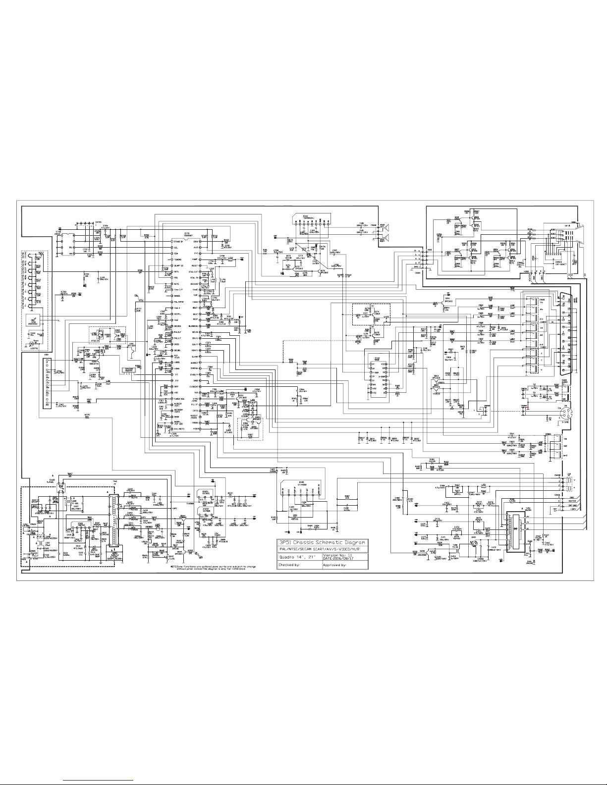
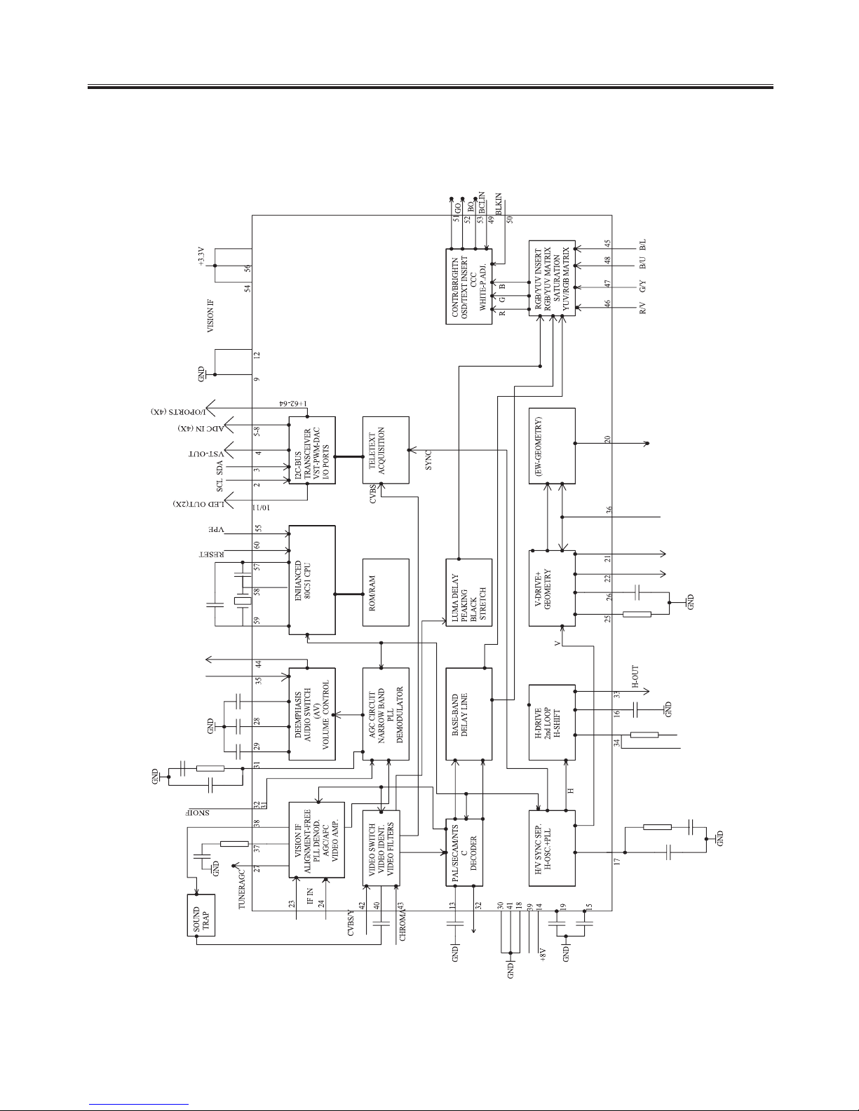
Chassis Block Diagram
/
63
62
15
5
14
AV
2
R
AV
2
L
AV
1
R
AV
1
L
A
B
9
10
12
3
1
AUDIO OUT
4052
AUDIO SWITCH
TDA7056A
3
5023
xx
0
(stereo)
(mono)
BF422/BF423
4
-5-
IC BLOCK DIAGRAM
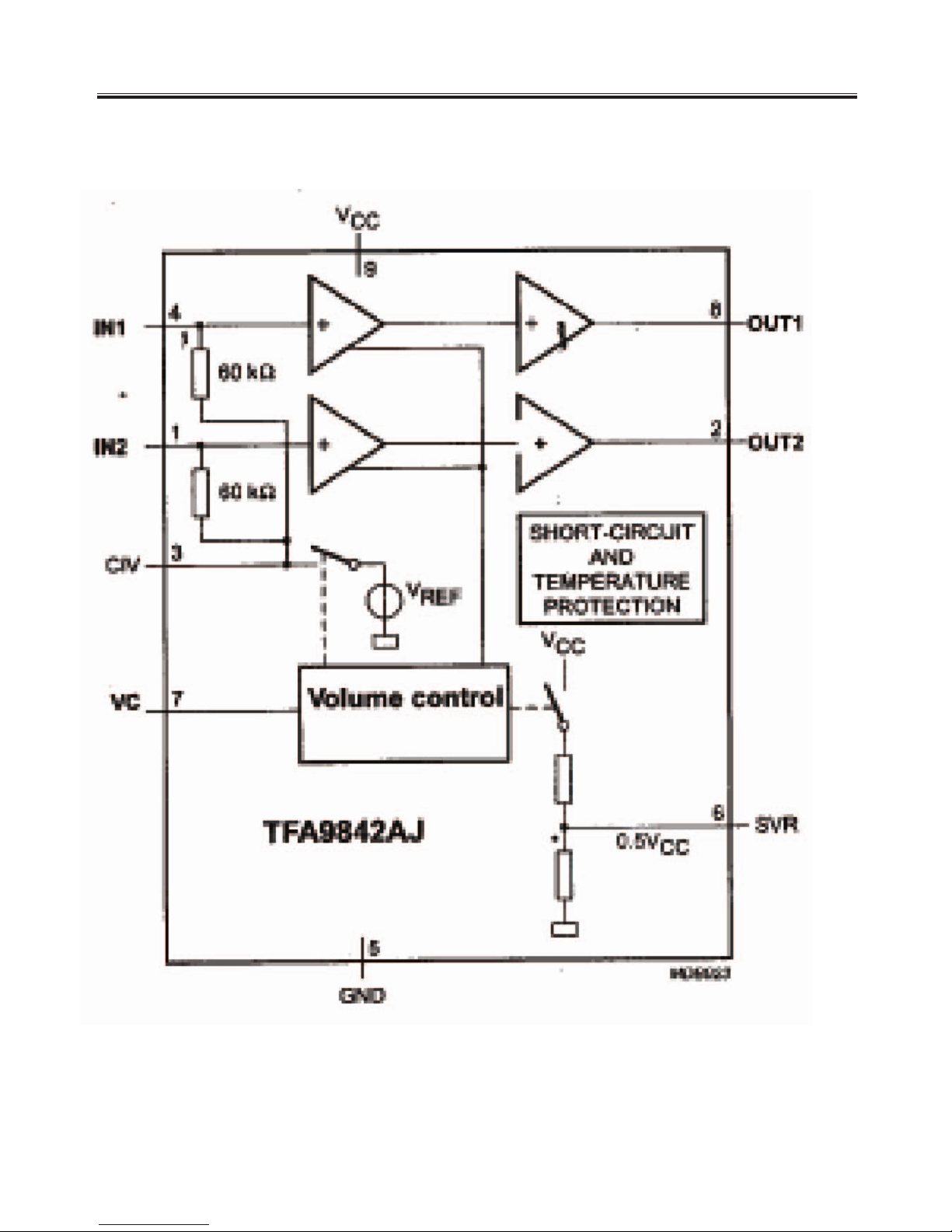
IC 101 TFA9842AJ(2Channel Audio Amplifier)
-6-
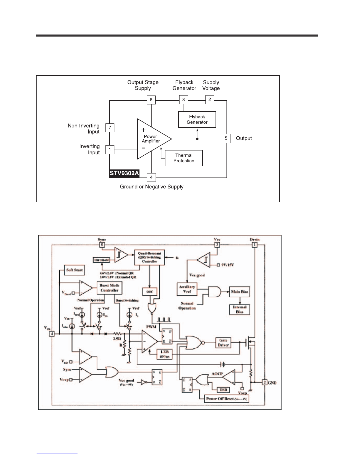
IC 401 (Vertical Deflection Booster) STV9302A
IC BLOCK DIAGRAM
IC 601 (Power Switch) F SCQ0765RT
-7-
1
INPUT
2
OUTPUT
SERIES
PASS
ELEMENT
SOA
PROTECTION
REFERENCE
VOLTAGE
ERROR
AMPLIFIER
THERRMAL
PROTECTION
STARTING
CIRCUIT
CURRENT
GENERATOR
REFERENCE
VOLTAGE
3
GND
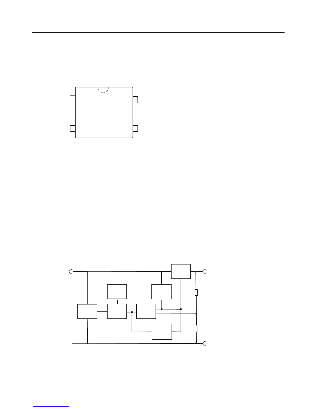
IC 652 (Regulators) L7808Series
1
2
3
4
1:ANODE
2:CATHODE
3:EMITTER
4:COLLECTOR
IC 602 (Photo Transistor ) TLP421
IC BLOCK DIAGRAM
TLP421
-8-
IC 701 ( TDA9381 TV Signal Processor)
IC BLOCK DIAGRAM
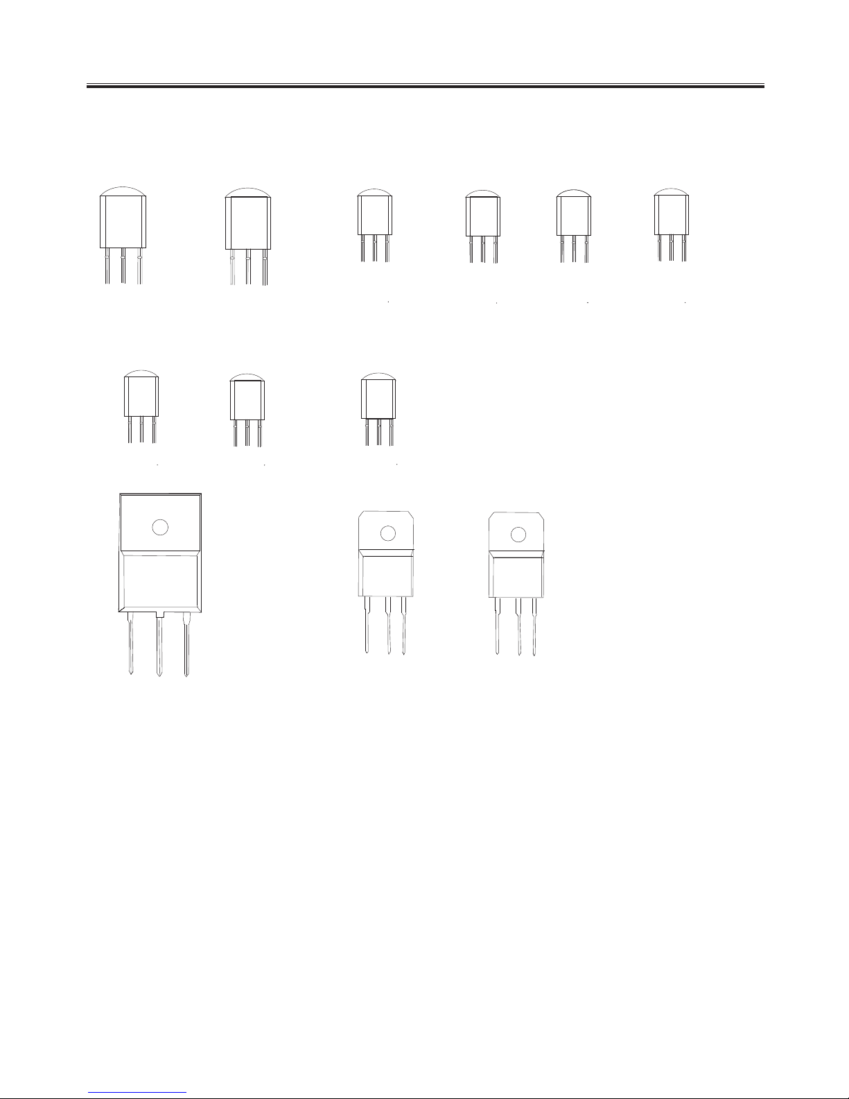
2DD2499
C
1
81
5
A101
5
PNP
NPN
L7805
INPUT
GND
OUTPUT
INPUT
L7808
INPUT
GND
OUTPUT
C
2482
C
B
E
NPN
-9-
C
B
E
A9
6
6
PNP
TRANSISTOR MARK
NPN
C
B
E
C
B
E
C
2
12
0
NPN
C
B
E
C
27
17
NPN
C
B
E
B
C
E
B
F
4
2
1
PNP
C
B
E
B
F
4
2
1
PNP
C
B
E
B
F
4
2
2
NPN
C
B
E
B
F
4
2
3
PNP
C
B
E
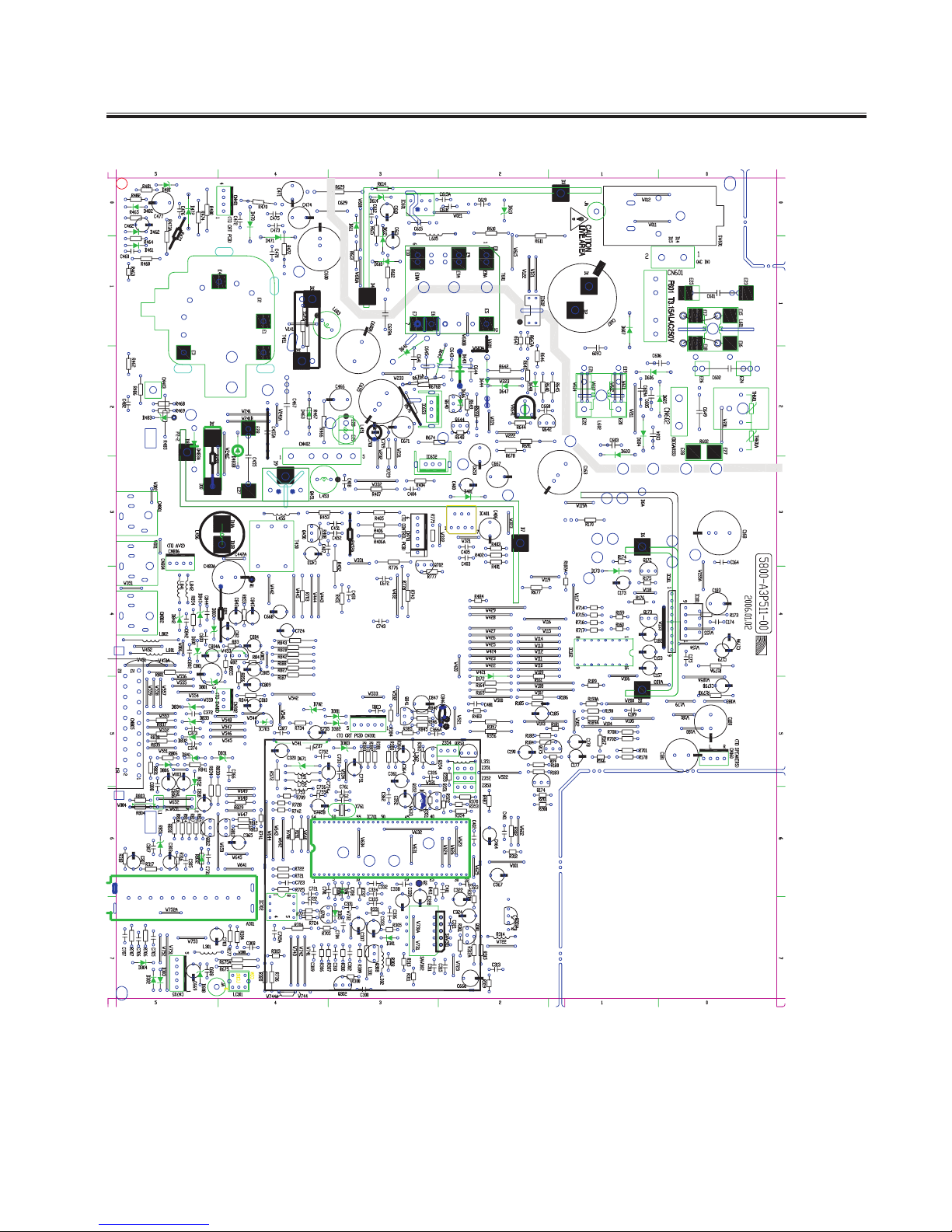
MAIN PCB Top Layer
-10-
 Loading...