

Page 1
Q-TECH
COR PORATI ON
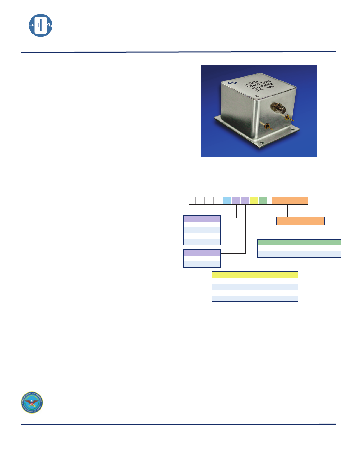
Description
Q-Tech’s High Stability Oven Controlled Crystal Oscillator
(OCXO) is a high reliability signal generator that provides Sine
wave or HCMOS output. The OCXO is designed to be used in
Aerospace applications.
It is designed to withstand radiation level up to 100kRad (*)
(total dose), high shock and vibration. The OCXO has very low
phase noise. Low G-Sensitivity SC-Cut Crystal utilized in the
design guarantees 1PPB/G or better. The reliable construction
of this design qualifies it for stringent environmental
applications.
(*) Please contact factory for higher level of radiation
hardness.
Features
• Made in the USA
• ITAR
• DFARS 252-225-7014 Compliant:
Electronic Component Exemption
• USML Registration # M17677
• Supply voltages 3.3Vdc to 15Vdc
• Wide temperature range (-40ºC to +85ºC)
• SC-Cut crystal
• Low phase noise and jitter
• Choice of output power and load
• Radiation Hardened
• Custom design available tailored to meet customer’s needs
• Q-Tech does not use pure lead or pure tin in its products
LOW PHASE NOISE, SPACE LEVEL OCXO
3.3 to 15Vdc - 1MHz to 125MHz
Ordering Information
(Sample part number)
QT4107SDM-55 . 0 0 0 M Hz
Q T 4 1 0 7 S D M- 55.000MHz
Supply Voltage:
3 = +3.3V
5 = +5.0V
6 = +12.0V
7 = +15.0V
Logic:
C = HCMOS
S = Sine Wave
Frequency vs. Temperature Code:
G = ± 100PPB at -20ºC to +70ºC
H = ± 10PPB at -20ºC to +70ºC
J = ± 200PPB at -40ºC to +85ºC
D = ± 20PPB at -40ºC to +85ºC
For Non-Standard requirements, contact Q-Tech Corporation at
Sales@Q-Tech.com
Blank=EM
Output Frequency
Screening Option:
M=Per MIL-PRF-55310, Level S
Applications
Packaging Options
• Designed to meet today’s requirements for Space Grade
applications
• Control and measurement
• Signal processing
• Standard packaging in black foam
Other Options Available For An Additional Charge
• P. I. N. D. test (MIL-STD 883, Method 2020)
• Phase Noise test (Static and under vibration)
• Jitter test
Specifications subject to change without prior notice.
ITAR Controlled
Q-TECH Corporation - 10150 W. Jefferson Boulevard, Culver City 90232 - Tel: 310-836-7900 - Fax: 310-836-2157 - www.q-te ch.co m
QPDS-0008 (Revision B, April 2013 )(ECO# 10835)
1 of 6
Page 2
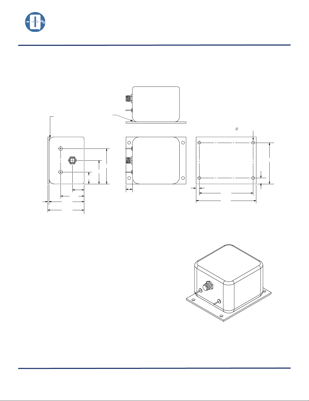
Q-TECH
.275
VCC
CASE IS WELDED TO .060 PLATE
BRAZE BASEPLATE TO CASE AROUND
ENTIRE PERIMETER PRIOR TO PLATING
OUT
GND
.060
1.490
1.560
1.550
1.000
.500
1.500
1.000
.500
2.560
2.555
4X
.125±.003 THRU
2.290
.135
1.750
.250
COR PORATI ON
LOW PHASE NOISE, SPACE LEVEL OCXO
3.3 to 15Vdc - 1MHz to 125MHz
Package Outline -
Dimensions are in inches
Package Information
• Package Material: CRS
• Weight: 165g typ., 175g max.
• Package Finish: Nickel Plating 500 micro Inches
• SMA Connector: Body = Brass (QQ-B-626), Nickel Plated
Q-TECH Corporation - 10150 W. Jefferson Boulevard, Culver City 90232 - Tel: 310-836-7900 - Fax: 310-836-2157 - www.q-te ch.co m
QPDS-0008 (Revision B, April 2013 )(ECO# 10835)
Contact Pin = BeCu, Gold Plated
Insulators = Teflon, MIL-P-19468
• Power Connetors: Gold Plated per MIL-G-45204C, Class 00
2 of 6
Page 3

Q-TECH
COR PORATI ON
LOW PHASE NOISE, SPACE LEVEL OCXO
3.3 to 15Vdc - 1MHz to 125MHz
Electrical Characteristics
Parameters Conditions Requirements
Output Frequency Range (Fo)
Supply Voltage (Vdd) ±5.0% +3.3Vdc, +5Vdc, +12Vdc and +15Vdc
Initial Tolerance @+25ºC ±0.2ppm
Temperature Range See Option Codes
Frequency Stability vs. Temperature See Option Codes
Frequency Stability vs. Voltage Variation Over Temperature Range ±10PPB
Frequency Stability vs. Load Variation ±5.0% Load Variation ±20PPB
Warm-up Power max. @-40ºC 4.8W
Steady State Power max. @+25ºC 2.7W
Warm-up Time @+25ºC to ±100PPB (2 hours ref.)
Output Waveform Sine Wave HCMOS
Output Power (See note 1) +3.0±1.0dBm
Output Power Stability (See note 2) Over Temperature Range
Duty Cycle Over Temperature Range 50%±5.0%
Output Load 50Ω 10kΩ//15pF
Harmonics Over Temperature Range -35dBc
Spurious (See note 3) Over Temperature Range -90dBc
Aging
G-Sensitivity max. 1PPB/G
Phase Noise for 50MHz OCXO (typ.)
Per Day 1PPB
15 years 1.5PPM
1Hz -70dBc/Hz
10Hz -102dBc/Hz
100Hz -132dBc/Hz
1kHz -148dBc/Hz
10kHz -155dBc/Hz
100kHz -155dBc/Hz
1MHz — 125MHz
10 min.
±1.0dBm
Other Design and Test Options
• Phase Noise and Jitter built to specification
including static and vibration.
• Low supply current
• QCI tests
• Tight frequency stability versus temperature,
supply voltage, and load variations
Notes:
1. The output level is determined by the supply
voltage, load, and package size.
2. Typical amplitude stability over temperature is
±10% or less.
3. Typical spurious level is better than -100dBc over
the spectrum of 100kHz to 1GHz.
• Low spurious (see note 3)
• Low frequency aging, Allan Variance
• High-shock resistant
Q-TECH Corporation - 10150 W. Jefferson Boulevard, Culver City 90232 - Tel: 310-836-7900 - Fax: 310-836-2157 - www.q-te ch.co m
QPDS-0008 (Revision B, April 2013 )(ECO# 10835)
3 of 6
Page 4

Q-TECH
COR PORATI ON
LOW PHASE NOISE, SPACE LEVEL OCXO
3.3 to 15Vdc - 1MHz to 125MHz
Environmental Specifications
Q-Tech Standard Screening similar to (MIL-PRF-55310) is available. Q-Tech can also customize screening and test procedures to meet
your specific requirements. The packages are designed and processed to exceed the following test conditions:
Environmental Test Test Conditions
Initial Accuracy at Reference Temperature MIL-PRF-55310, Type 4, Class 3
Frequency Warm-up MIL-PRF-55310, Type 4, Class 3
Initial Frequency-Temperature Accuracy MIL-PRF-55310 (4.8.10.1)
Frequency-Voltage Tolerance MIL-PRF-55310
Frequency-Load Tolerance MIL-PRF-55310
Phase Noise Steady-State MIL-PRF-55310
Phase Noise Random Vibration MIL-PRF-55310
Output Power (Sinusoidal Waveform) MIL-PRF-55310
Output Logic Voltage Levels (Square wave ) MIL-PRF-55310
Rise Time and Fall Time (Square wave ) MIL-PRF-55310
Duty Cycle (Square wave ) MIL-PRF-55310
Harmonic and Sub-harmonic Distortion MIL-PRF-55310
Spurious Response MIL-PRF-55310
Oven Input Current-Power MIL-PRF-55310, Type 4, Class 3
Temperature Cycling MIL-STD-883, Method 1010, Cond. B
Constant Acceleration MIL-STD-883, Method 2001, Cond. A, Y1
Seal Fine Leak MIL-STD-883, Method 1014, Cond. A & C
Burn-in 240 hours, At highest operating temperature with load
Aging 30 days, MIL-PRF-55310, Type 4, Class 3
Random Vibration MIL-STD-883, Method 2026
Shock, Non Operating MIL-STD-883, Method 2002
Thermal Shock, Non Operating MIL-STD-202, Method 107, Cond. B
Ambient Pressure MIL-STD-202, 105, Cond. G, 5 minutes dwell time minimum
Resistance to Solder Heat MIL-STD-202, Method 210, Cond. C
Terminal Strength MIL-STD-202, Method 211, Cond. C
Resistance to Solvents MIL-STD-202, Method 215
Solderability MIL-STD-202, Method 208
ESD Classification MIL-STD-883, Method 3015, Class 1HBM 0 to 1,999V
Non-destructive Bond Pull MIL-STD-883, Method 2023
Please contact Q-Tech for higher shock requirements
Q-TECH Corporation - 10150 W. Jefferson Boulevard, Culver City 90232 - Tel: 310-836-7900 - Fax: 310-836-2157 - www.q-te ch.co m
QPDS-0008 (Revision B, April 2013 )(ECO# 10835)
4 of 6
Page 5

Q-TECH
COR PORATI ON
LOW PHASE NOISE, SPACE LEVEL OCXO
3.3 to 15Vdc - 1MHz to 125MHz
Design and Construction
The design and construction of the crystal oscillator shall be as specified herein. As a minimum, the oscillators shall meet the design and
construction requirements of MIL-PRF-55310.
Element De-rating
All active and passive elements shall be derated in accordance with the applicable hybrid microcircuit element requirements of
MIL-STD-975. Elements shall not operate in excess of de-rated values.
Worst Case Circuit Analysis
Worst case analysis shall be based on:
a. Maximum rated value
b. The worst case design value
c. Derating factor for each element
d. Temperature variation
e. Radiation
MTBF
Mean Time between Failure analysis shall be done based on MIL-HDBK-217
Element Evaluation
All piece parts shall be derived from lots that meet the element evaluation requirements of MIL-PRF-38534, Class K except for
the following exceptions:
Active Elements
a) Visual inspection of silicon on sapphire microcircuits. Semicircular crack(s) or multiple adjacent cracks, not in the active
area, starting and terminating at the edge of the die are acceptable. Attached (chip in place) sapphire is nonconductive
material and shall not be considered as foreign material and will be considered as nonconductive material for all
inspection criteria.
b) Subgroup 4, Scanning Electron Microscope (SEM) inspection. The manufacturer may allow the die distributor, at his
option, select two (2) dice from a waffle pack (containing a maximum quantity of 100 die), visually inspect for the worst
case metallization of the 2 dice, and take SEM photographs of the worst case.
c) Subgroup 5 radiation tests. Subgroup 5 radiation tests are not required unless otherwise specified in the detail
specification.
Package Elements
a) Salt spray. Salt spray testing is not required.
Quartz Crystal Material
Unless otherwise specified by the detail specification, the quartz Crystal material shall be swept synthetic, grade 2.2 or better.
Crystal Mounting
The crystal element shall be four-point mounted in such a manner as to assure adequate crystal performance when the oscillator
is subjected to the environmental conditions specified herein.
Q-TECH Corporation - 10150 W. Jefferson Boulevard, Culver City 90232 - Tel: 310-836-7900 - Fax: 310-836-2157 - www.q-te ch.co m
QPDS-0008 (Revision B, April 2013 )(ECO# 10835)
5 of 6
Page 6

Q-TECH
COR PORATI ON
LOW PHASE NOISE, SPACE LEVEL OCXO
3.3 to 15Vdc - 1MHz to 125MHz
Phase Noise and Phase Jitter Integration
Phase noise is measured in the frequency domain, and is expressed as a ratio of signal power to noise power measured in a 1Hz bandwidth
at an offset frequency from the carrier, e.g. 10Hz, 100Hz, 1kHz, 10kHz, 100kHz, etc. Phase noise measurement is made with an Agilent
E5052A Signal Source Analyzer (SSA) with built-in outstanding low-noise DC power supply source. The DC source is floated from the
ground and isolated from external noise to ensure accuracy and repeatability.
In order to determine the total noise power over a certain frequency range (bandwidth), the time domain must be analyzed in the frequency
domain, and then reconstructed in the time domain into an RMS value with the unwanted frequencies excluded. This may be done by
converting L(f) back to Sφ(f) over the bandwidth of interest, integrating and performing some calculations.
Symbol
∫L(f)
Sφ (f)=(180/Π)x√2 ∫L(f)df
RMS jitter = Sφ (f)/(fosc.360°) Jitter(in seconds) due to phase noise. Note Sφ (f) in degrees.
Integrated single side band phase noise (dBc)
Spectral density of phase modulation, also known as RMS phase error (in degrees)
Definition
The value of RMS jitter over the bandwidth of interest, e.g. 10kHz to 20MHz, 10Hz to 20MHz, represents 1 standard deviation of
phase jitter contributed by the noise in that defined bandwidth.
Typical Phase Noise of 50MHz OCXO
ECO REV REVISION SUMMARY Page
10572
10835
Q-TECH Corporation - 10150 W. Jefferson Boulevard, Culver City 90232 - Tel: 310-836-7900 - Fax: 310-836-2157 - www.q-te ch.co m
QPDS-0008 (Revision B, April 2013 )(ECO# 10835)
A Change from ECCN:EAR99 to ITAR 1
Fixed typo under “Other Design and Test Options” (from see note 5 to 3) 3
B
Add document # on footer (QPDS-0008) All
6 of 6
 Loading...