

Page 1
Q-TECH
COR PORATI ON
Description
The Q-Tech Sine Wave Sources encompasses state-of-the-art
sinewave source with low harmonic distortion and a precise
sinewave output.
A flexible design allows Q-Tech Corporation to offer a
variety of choices of output power and load. Based on this
flexibility, Q-Tech welcomes specifications with parameters
other than standard. An external trimming capacitor option
is available for applications that require a tight frequency
stability.
The AT-Cut crystal utilized in the design allows for high
stability for a particular temperature range extending from
-55ºC to +125ºC. For more information, please refer to the
stability vs. temperature on the following page.
The reliable construction of these sinewave oscillators
qualifies them for more stringent environmental
applications. Military screening per MIL-PRF-55310, Level
B is available as an option.
Features
• Made in the USA
• ECCN: EAR99
• DFARS 252-225-7014 Compliant:
Electronic Component Exemption
• USML Registration # M17677
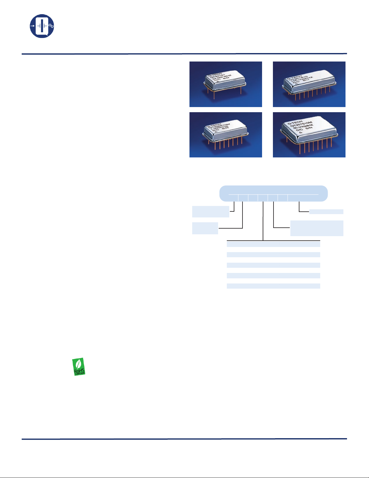
• Available in both DIP and Double DIP packages
• Supply voltages 5Vdc and 15Vdc
• Broad frequency range from 10Hz to 450MHz
• AT-Cut crystal
• Low Total Harmonic Distortion
• Choice of output power and load
• All metal and hermetically sealed packages
• Low phase noise
• External tuning capacitor option
• Fundamental and third overtone designs
• Analog multiplier for frequency ≥ 200MHz
• Tristate option
• Custom design available tailors to meet customer’s needs
• Q-Tech does not use pure lead or pure tin in its products
• RoHS compliant
Applications
• Designed to meet today’s requirements for communication
systems.
• Wide military clock applications
• Control and measurement
• Signal processing
SINE WAVE SOURCES
DUAL-IN-LINE CRYSTAL CLOCK OSCILLATORS
5.0 to 15Vdc - 10Hz to 450MHz
Ordering Information
Sample part number
QT901S9M-20. 0 0 0 M H z
QT 901 S9M-20.000MHz
T = Standard
S = Solder Dip (*)
Model #
(See page 3)
1 = ± 100ppm at 0ºC to +70ºC
3(***) = ± 5ppm at 0ºC to +50ºC
4 = ± 50ppm at 0ºC to +70ºC
5 = ± 25ppm at -20ºC to +70ºC
6 = ± 50ppm at -55ºC to +105ºC
9 = ± 50ppm at -55ºC to +125ºC
10 = ± 100ppm at -55ºC to +125ºC
11 = ± 50ppm at -40ºC to +85ºC
12 = ± 100ppm at -40ºC to +85ºC
(*) Hot Solder Dip Sn60 per MIL-PRF 55310 is optional for an additional cost
(***) Requires an external capacitor
For custom load, supply voltage, output power, harmonic distortion, frequency
stability vs. temperature, and others not listed herein, please request a custom part
number.
For Non-Standard requirements, contact Q-Tech Corporation at
Sales@Q-Tech.com
Screened to
MIL-PRF-55310,level B
(Left blank if no screening)
Packaging Options
• Standard packaging in black foam
• Optional anti-static plastic tube
Other Options Available For An Additional Charge
• Lead forming available on all packages. Please contact for details.
• P. I. N. D. test (MIL-STD 883, Method 2020)
• Lead trimming
• Phase Noise test (Static and under vibration)
• Jitter test
All DIP packages are available in surface mount form.
Specifications subject to change without prior notice.
Output frequency
Q-TECH Corporation - 10150 W. Jefferson Boulevard, Culver City 90232 - Tel: 310-836-7900 - Fax: 310-836-2157 - www.q-tec h.com
Sine Wave Sources (Revision E, August 2010 ) (ECO# 9936)
1
Page 2

Q-TECH
COR PORATI ON
SINE WAVE SOURCES
DUAL-IN-LINE CRYSTAL CLOCK OSCILLATORS
5.0 to 15Vdc - 10Hz to 450MHz
Electrical Characteristics
Parameters QT901S
Output freq. range (Fo)
Supply voltage (Vdd)
Maximum Applied Voltage (Vdd max.) +18Vdc -0.5 to +7.0Vdc
Frequency stability (∆F/∆T) See Option codes
Operating temp. (Topr)
Storage temp. (Tsto) -62ºC to + 125ºC
Operating supply current (Idd)
Output amplitude or power 1V RMS min.
Output Load 1kΩ 50Ω
Total Harmonic Distortion (THD) or
harmonics
Sub-harmonics
Start-up time
Phase Noise at 25ºC (typ.) at:
Integrated Phase Jitter RMS
(12kHz to 20MHz) typ.
Aging (at 70ºC) ± 5ppm max. first year / ± 2ppm typ. per year thereafter
10Hz — 1MHz (*) 1MHz — 85MHz (**) 10Hz — 450MHz (*)
+15Vdc ± 5% +5Vdc ± 10%
20mA max. 40mA max.
2V RMS typ.
5% max. -20dBc max.
QT906S
See Option codes
20mA typ. at 25MHz
30mA typ. at 50MHz
0dBm min.
+5dBm typ.
Internally AC coupled
-30dBc max.
10ms max.
10Hz -70dBc/Hz
100Hz -100dBc/Hz
1kHz -125dBc/Hz
10kHz -140dBc/Hz
100kHz -145dBc/Hz
QT941S QT957S
1V p-p min. for Fo < 1MHz
0dBm min. for F ≥1MHz
1ps
60mA max.
40mA typ. at 175MHz
1kΩ for Fo < 1MHz
50Ω for Fo ≥ 1MHz
Other Design and Test Options
Sine Wave options are available with a Q-Tech
MCM part number:
• Supply voltage +5Vdc to +18Vdc
• Output power -10dBm to +13dBm into 50Ω
(see note 1)
• Harmonics better than -20dBc (see note 2)
• Sub-harmonics better than -30dBc (see note 3)
• Amplitude stability versus temperature to
within ±1% (see note 4)
• VCXO Sine Output (see details in VCXO data
sheets)
• Phase Noise and Jitter built to specification
including static and vibration.
• Low supply current
• QCI tests
• Tight frequency stability versus temperature,
supply voltage, and load variations
• Low g-sensitivity and low phase noise
• Low spurious (see note 5)
• Low Harmonic Distortion (THD < 5%)
• Low frequency aging, Allan Variance
• High-shock resistant
Notes:
1. The output level is determined by the supply
voltage, load, and package size.
2. A specified harmonic level of -20dBc is easily
achievable. The typical harmonics of Q-Tech Sine
Wave source are better than -25dBc.
3. Sub-harmonic level is determined by frequency
multiplication method, supply voltage, output
power, and input current.
4. Typical amplitude stability over temperature is
±10% or less.
5. Typical spurious level is better than -60dBc over the
spectrum of 100kHz to 1GHz.
(*) Frequencies less than 500Hz require an external 1µF AC coupling capacitor at the output pin.
(**) Higher frequencies are available with a Q-Tech custom part number.
Q-TECH Corporation - 10150 W. Jefferson Boulevard, Culver City 90232 - Tel: 310-836-7900 - Fax: 310-836-2157 - www.q-t ech.co m
Sine Wave Sources (Revision E, August 2010 ) (ECO# 9936)
2
Page 3

Q-TECH
19
1018
.300
.505
.200
.018
.800
1.080
Q-TECH
P/N
FREQ.
D/C S/N
(12.83)
(7.62)
Ø .056
Ø 1.42
.100
(2.54)
(20.32)
(27.43)
(.457)
(5.08)
.200
(5.08)
MAX.
MIN.
MAX.
(5.08)
.200
.250
(6.35)
.018
(0.457)
.100
(2.54)
.700
(17.78)
.980
(24.89)
.600
(15.24)
(20.45)
.805
FREQ.
P/N
Q-TECH
D/C S/N
81
16 9
MAX.
MIN.
MAX.
MAX.
17
814
Q-TECH
P/N
FREQ.
D/C S/N
(22.35)
(15.24)
.880
.600
.300
(7.62)
(2.54)
.100
.505
(12.83)
MAX.
(.457)
.018
MIN.
(5.08)
.200
.200
(5.08)
MAX.
MAX.
14 8
71
FREQ.
D/C S/N
P/N
Q-TECH
.600
(15.24)
(7.62)
.300
.200
(5.08)
MAX.
MIN.
(5.08)
.200
(.457)
.018
MAX.
(20.32)
.800
.505
(12.83)
MAX.
COR PORATI ON
Package Configuration Versus Pin Connections
SINE WAVE SOURCES
DUAL-IN-LINE CRYSTAL CLOCK OSCILLATORS
5.0 to 15Vdc - 10Hz to 450MHz
A
QT901S
D
QT957S
B
QT906S
C
QT941S
Q-TECH Corporation - 10150 W. Jefferson Boulevard, Culver City 90232 - Tel: 310-836-7900 - Fax: 310-836-2157 - www.q-tec h.com
Sine Wave Sources (Revision E, August 2010 ) (ECO# 9936)
Dimensions are in inches (mm)
QT # Conf Vcc GND Case Output
MIL-PRF-55310
Configuration
QT901S A 18 9 9 10 N/A
QT906S B 14 7 7 8 N/A
QT941S C 14 7 7 8 N/A
QT957S D 16 8 8 9 N/A
Please contact factory for pin connections on external capacitor (code 3).
Package Information
• Lead material: Kovar
• Lead finish: Gold Plated: 50μ ~ 80μ inches
Nickel Underplate: 100μ ~ 250μ inches
• Package to lid attachment: Resistance weld
• Weight: 4.0g typ., 14.2g max.
Equivalent
3
Page 4

Q-TECH
Vcc
Out
GND
QT906S
QT941S
QT957S
+5Vdc
OUTPUT
0.01µF
50
Vcc
Out
GND
QT901S
+15Vdc
OUTPUT
0.01uF
1k
Vcc
Out
GND
QT901S(<500Hz)
+15V
OUTPUT
0.01µF
1k
1µF
COR PORATI ON
SINE WAVE SOURCES
DUAL-IN-LINE CRYSTAL CLOCK OSCILLATORS
5.0 to 15Vdc - 10Hz to 450MHz
Output Waveform into 50Ω load
Typical output amplitude of QT957S-69.4MHz
Test Circuit
Startup Time
Sine Wave Sources (Revision E, August 2010 ) (ECO# 9936)
Typical spectrum output power and harmonics of QT957S-171MHz
Q-TECH Corporation - 10150 W. Jefferson Boulevard, Culver City 90232 - Tel: 310-836-7900 - Fax: 310-836-2157 - www.q-tec h.com
Typical output amplitude and start-up time of QT957S-20.0166MHz
4
Page 5

Q-TECH
45º 45º
Hybrid Case
Substrate
Die
D/A epoxy
D/A epoxy
Heat
Die
R1
D/A epoxy
Substrate
D/A epoxy
Hybrid Case
R2 R3 R4 R5
JA JC CA
Die
T
T
T
C
A
J
CA
JC
COR PORATI ON
Thermal Characteristics
The heat transfer model in a hybrid package is described in
figure 1 (Based on single ASIC design).
Heat spreading occurs when heat flows into a material layer of
increased cross-sectional area. It is adequate to assume that
spreading occurs at a 45° angle.
The total thermal resistance is calculated by summing the
thermal resistances of each material in the thermal path
between the device and hybrid case.
SINE WAVE SOURCES
DUAL-IN-LINE CRYSTAL CLOCK OSCILLATORS
5.0 to 15Vdc - 10Hz to 450MHz
RT = R1 + R2 + R3 + R4 + R5
(Figure 1)
The total thermal resistance RT (see figure 2) between the heat
source (die) to the hybrid case is the Theta Junction to Case
(Theta JC) in°C/W.
• Theta junction to case (Theta JC) for this product is 24°C/W.
• Theta case to ambient (Theta CA) for this part is 106°C/W.
• Theta Junction to ambient (Theta JA) is 130°C/W.
Maximum power dissipation PD for this package at 25°C is:
• PD(max) = (TJ (max) – TA)/Theta JA
• With TJ = 175°C (Maximum junction temperature of die)
• PD(max) = (175 – 25)/130 = 1.15W
(Figure 2)
Environmental Specifications
Q-Tech Standard Screening/QCI (MIL-PRF55310) is available for all of our Sine Wave packages. Q-Tech can also customize
screening and test procedures to meet your specific requirements. The Sine Wave packages are designed and processed to exceed the
following test conditions:
Environmental Test Test Conditions
Temperature cycling MIL-STD-883, Method 1010, Cond. B
Constant acceleration MIL-STD-883, Method 2001, Cond. A, Y1
Seal: Fine and Gross Leak MIL-STD-883, Method 1014, Cond. A and C
Burn-in 160 hours, 125°C with load
Aging 30 days, 70°C
Vibration sinusoidal MIL-STD-202, Method 204, Cond. D
Shock, non operating MIL-STD-202, Method 213, Cond. I
Thermal shock, non operating MIL-STD-202, Method 107, Cond. B
Ambient pressure, non operating MIL-STD-202, 105, Cond. C, 5 minutes dwell time minimum
Resistance to solder heat MIL-STD-202, Method 210, Cond. C
Moisture resistance MIL-STD-202, Method 106
Terminal strength MIL-STD-202, Method 211, Cond. C
Resistance to solvents MIL-STD-202, Method 215
Solderability MIL-STD-202, Method 208
ESD Classification MIL-STD-883, Method 3015, Class 1HBM 0 to 1,999V
Moisture Sensitivity Level J-STD-020, MSL=1
Q-TECH Corporation - 10150 W. Jefferson Boulevard, Culver City 90232 - Tel: 310-836-7900 - Fax: 310-836-2157 - www.q-tec h.com
Sine Wave Sources (Revision E, August 2010 ) (ECO# 9936)
Please contact Q-Tech for higher shock requirements
5
Page 6

SINE WAVE SOURCES
-50
-40
-30
-20
-10
0
10
20
30
40
50
-55 -50 -45 -40 -35 -30 -25 -20 -15 -10 -5 0510 15 20 25 30 35 40 45 50 55 60 65 70 75 80 85 90 95 100 105 110 115 120 125
Temperature (°C)
1_12 2_12
Frequency Stability (PPM)
FREQUENCY STABILITY VS. TEMPERATURE QT957S-64MHz
Q-TECH
COR PORATI ON
Frequency vs. Temperature Curve
Phase Noise and Phase Jitter Integration
Phase noise is measured in the frequency domain, and is expressed as a ratio of signal power to noise power measured in a 1Hz
bandwidth at an offset frequency from the carrier, e.g. 10Hz, 100Hz, 1kHz, 10kHz, 100kHz, etc. Phase noise measurement is made
with an Agilent E5052A Signal Source Analyzer (SSA) with built-in outstanding low-noise DC power supply source. The DC source
is floated from the ground and isolated from external noise to ensure accuracy and repeatability.
DUAL-IN-LINE CRYSTAL CLOCK OSCILLATORS
5.0 to 15Vdc - 10Hz to 450MHz
In order to determine the total noise power over a certain frequency range (bandwidth), the time domain must be analyzed in the
frequency domain, and then reconstructed in the time domain into an rms value with the unwanted frequencies excluded. This may be
done by converting L(f) back to Sφ(f) over the bandwidth of interest, integrating and performing some calculations.
Symbol
∫L(f)
Sφ (f)=(180/Π)x√2 ∫L(f)df
RMS jitter = Sφ (f)/(fosc.360°) Jitter(in seconds) due to phase noise. Note Sφ (f) in degrees.
Integrated single side band phase noise (dBc)
Spectral density of phase modulation, also known as RMS phase error (in degrees)
Definition
The value of RMS jitter over the bandwidth of interest, e.g. 10kHz to 20MHz, 10Hz to 20MHz, represents 1 standard deviation of
phase jitter contributed by the noise in that defined bandwidth.
Figure below shows a typical Phase Noise/Phase jitter of a QT957S, +5Vdc, 150MHz and QT957S8M, +5Vdc, 69.4MHz clock at offset frequencies 10Hz to 10MHz, and phase jitter integrated over the bandwidth of 12kHz to 1MHz.
Q-TECH Corporation - 10150 W. Jefferson Boulevard, Culver City 90232 - Tel: 310-836-7900 - Fax: 310-836-2157 - www.q-tec h.com
Sine Wave Sources (Revision E, August 2010 ) (ECO# 9936)
QT957S, +5Vdc, 150MHz
QT957S8M, 5.0Vdc, 69.4 MHz
6
 Loading...