

Page 1
C1
C1
QT92
7x5mm
7x5mm
QT92
(2.2)
0.087
(1.81)
0.071
(2.0)
0.079
(2.88)
0.11
(2.2)
0.087
(1.81)
0.071
(2.88)
0.11
(3.3)
0.130
Q-TECH
6 X
0.290±0.005
0.190 MAX.
(1.396±0.13)
0.200±.005
0.048±.002
(1.22±0.051)
(7.37±0.13)
(5.08±0.13)
0.100±.005
(2.54±0.13)
(4.826 MAX.)
(.203) (2.794±0.13)
(8.00 max.)
0.315 max.
0.055±.005
0.008
0.110±.005
0.018±.003
(.457±0.076)
12
4 3
0.350±.0.005
(8.89±0.13)
P/N
FREQ.
Q-TECH
D/C S/N
COR PORATI ON
Description
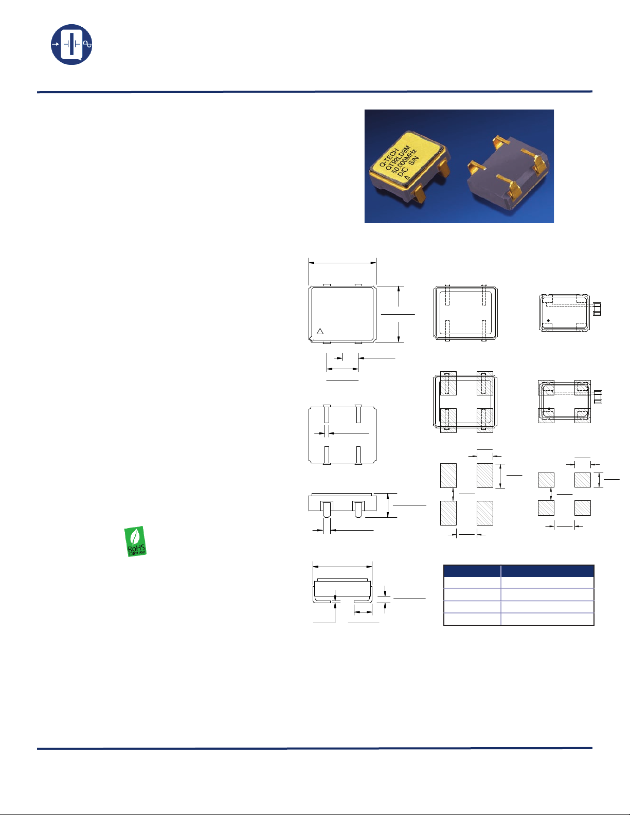
Q-Tech’s surface-mount QT92 Series oscillators consist of
an IC 5Vdc, 3.3Vdc, 2.5Vdc, 1.8Vdc clock square wave
generator and a round AT high-precision quartz crystal built
in a rugged surface-mount ceramic miniature package. It
was designed to be replaceable and retrofitable into the
footprint of a 7 x 5mm COTS oscillator.
QT92 SERIES
HIGH-RELIABILITY MINIATURE CLOCK OSCILLATORS
1.8 to 5.0Vdc - 15kHz to 160MHz
Features
• Made in the USA
• ECCN: EAR99
• DFARS 252-225-7014 Compliant:
Electronic Component Exemption
• USML Registration # M17677
• Drop in replacement for 7 x 5mm COTS oscilla-
tor with built-in by-pass capacitor
• Smallest AT round crystal package ever designed
• Available as QPL MIL-PRF-55310/37 and /38
• Able to meet 36000G shock per ITOP 1-2-601
• Radiation tolerant to 10K RAD
• Broad frequency range from 15kHz to 160MHz
• Rugged 4 point mount design for high shock and
vibration
• ACMOS, HCMOS, TTL or LVHCMOS logic
• Tri-State Output Option (D)
• Hermetically sealed ceramic SMD package
• Fundamental and 3rd Overtone designs
• Low phase noise
• Custom designs available
• Q-Tech does not use pure lead or pure tin in its
products
• RoHS compliant
Applications
• Designed to meet today’s requirements for low voltage
applications
• Wide military clock applications
• Gun launched munitions and systems
• Benign space environments
• Smart munitions
• Navigation
• Industrial controls
• Microcontroller driver
• Down-hole applications up to +200ºC
Q-TECH Corporation - 10150 W. Jefferson Boulevard, Culver City 90232 - Tel: 310-836-7900 - Fax: 310-836-2157 - www.q-t ech.c om
QT92 (Revision J, January 2011) (ECO #10089)
Package Specifications and Outline
Layout comparison of QT92 vs. 7x5mm
Pin No.
1
2
3
4
Dimensions are in inches (mm)
Package Information
• Package material: 90% AL2O
• Lead material: Kovar
3
Function
TRISTATE or NC
GND/CASE
OUTPUT
VDD
• Lead finish: Gold Plated: 50μ ~ 80μ inches
Nickel Underplate: 100μ ~ 250μ inches
• Weight: 0.6g typ., 3.0g max.
1
Page 2

Q-TECH
COR PORATI ON
Electrical Characteristics
QT92 SERIES
HIGH-RELIABILITY MINIATURE CLOCK OSCILLATORS
1.8 to 5.0Vdc - 15kHz to 160MHz
Parameters QT92AC QT92HC
Output frequency range (Fo)
Supply voltage (Vdd) 5.0Vdc ± 10%
Maximum Applied Voltage
(Vdd max.)
Frequency stability (∆F/∆T)
Operating temperature (Topr)
Storage temperature (Tsto)
Operating supply current
(Idd) (No Load)
Symmetry
(50% of ouput waveform or
1.4Vdc for TTL)
Rise and Fall times
(with typical load)
Output Load
500kHz — 85.000MHz
6ns max. - Fo < 30MHz
3ns max. - Fo ≥ 30 - 85MHz
(between 10% to 90%)
15pF // 10kohms
50pF max. or 10TTL
for (Fo < 60MHz)
30pF max. or 6TTL
for (Fo ≥ 60MHz)
15kHz — 85.000MHz(*)
-0.5 to +7.0Vdc -0.5 to +5.0Vdc
20 mA max. - 15kHz ~ < 16MHz
25 mA max. - 16MHz ~ < 32MHz
35 mA max. - 32MHz ~ < 60MHz
45 mA max. - 60MHz ~ ≤ 85MHz
45/55% max. - 15kHz ~ < 16MHz
40/60% max. - 16 ~ ≤ 85MHz
(Tighter symmetry available)
6ns max. - Fo < 30MHz
3ns max. - Fo ≥ 30 - 85MHz
(between 10% to 90%)
15pF // 10kohms
(2LSTTL)
QT92T QT92L
500kHz — 85.000MHz 125kHz — 160.000MHz (*)
3.3Vdc ± 10%
See Option codes
See Option codes
-62ºC to + 125ºC
3 mA max. - 125kHz ~ < 500kHz
6 mA max. - 500kHz ~ < 16MHz
10 mA max. - 16MHz ~ < 32MHz
20 mA max. - 32MHz ~ < 60MHz
30 mA max. - 60MHz ~ < 100MHz
40 mA max. - 100MHz ~ < 130MHz
50 mA max. - 130MHz ~ ≤160MHz
45/55% max. - 125kHz ~ < 16MHz
40/60% max. - 16 ~ ≤ 160MHz
(Tighter symmetry available)
5ns max. - Fo < 30MHz
3ns max. - Fo ≥ 30 - 85MHz
(between 0.8V to 2.0V)
10TTL (Fo < 60MHz)
6TTL (Fo ≥ 60MHz)
6ns max. - 125kHz ~ < 40MHz
3ns max. - 40 ~ ≤ 16 0MHz
(between 10% to 90%)
15pF // 10kohms
(30pF max. for F ≤ 50MHz)
QT92N
125.000kHz — 133.000MHz
2.5Vdc ± 10%
3 mA max. - 125kHz ~ < 500kHz
6 mA max. - 500kHz ~ < 40MHz
15 mA max. - 40MHz ~ < 60MHz
25 mA max. - 60MHz ~ < 85MHz
35 mA max. - 85MHz ~ ≤ 133MHz
45/55% max. - 125kHz ~ < 16MHz
40/60% max. - 16 ~ ≤ 133MHz
(Tighter symmetry available)
5ns max. - 125kHz ~ < 40MHz
3ns max. - 40 ~ ≤ 133MHz
(between 10% to 90%)
15pF // 10kohms
QT92R
125.000kHz — 100.000MHz
1.8Vdc ± 10%
4 mA max. - 125kHz ~ < 40MHz
10 mA max. - 40MHz ~ < 50MHz
20 mA max. - 50MHz ~ < 85MHz
25 mA max. - 85MHz ~ ≤ 100MHz
45/55% max. - 125kHz~ < 16MHz
40/60% max. - 16 ~ ≤ 100MHz
(Tighter symmetry available)
5ns max. - 125kHz ~ < 40MHz
3ns max. - 40 ~ ≤ 100MHz
(between 10% to 90%)
Start-up time (Tstup)
Output voltage (Voh/Vol)
Output Current (Ioh/Iol)
Enable/Disable
Tristate function Pin 1
Jitter RMS 1σ (at 25ºC)
Aging (at 70ºC)
0.9 x Vdd min.; 0.1 x Vdd max. 2.4V min.; 0.4V max.
± 24mA max.
± 8mA max.
VIH ≥ 2.2V Oscillation;
VIL ≤ 0.8V High Impedance
8ps typ. - < 40MHz
5ps typ. - ≥ 40MHz
(*) Some frequencies lower than 500kHz may not be available with tristate function
-1.6 mA/TTL
+40 µA/TTL
± 5ppm max. first year / ± 2ppm max. per year thereafter
5ms max.
0.9 x Vdd min.; 0.1 x Vdd max.
± 4mA max.
VIH ≥ 0.7 x Vdd Oscillation;
VIL ≤ 0.3 x Vdd High Impedance
15ps typ. - < 40MHz
8ps typ. - ≥ 40MHz
Q-TECH Corporation - 10150 W. Jefferson Boulevard, Culver City 90232 - Tel: 310-836-7900 - Fax: 310-836-2157 - www.q-te ch.com
QT92 (Revision J, January 2011) (ECO #10089)
2
Page 3

Q-TECH
COR PORATI ON
Ordering Information
Sample part number
QT92HCD9M-85 . 0 0 0 M Hz
QT92 HC D9M-85.000MHz
5.0Vdc
QT92 SERIES
HIGH-RELIABILITY MINIATURE CLOCK OSCILLATORS
1.8 to 5.0Vdc - 15kHz to 160MHz
3.3Vdc
Sample part number
QT92LD6M-150 . 0 0 0 M Hz
QT92 LD6M-150.000MHz
T = Standard
S = Solder Dip (*)
Logic:
AC = ACMOS
HC = HCMOS
T = TTL
Tristate Option
Blank = No Tristate
D = Tristate
Frequency vs. Temperature Code:
1 = ± 100ppm at 0ºC to +70ºC
4 = ± 50ppm at 0ºC to +70ºC
5 = ± 25ppm at -20ºC to +70ºC
6 = ± 50ppm at -55ºC to +105ºC
9 = ± 50ppm at -55ºC to +125ºC
10 = ± 100ppm at -55ºC to +125ºC
11 = ± 50ppm at -40ºC to +85ºC
12 = ± 100ppm at -40ºC to +85ºC
14 = ± 20ppm at -20ºC to +70ºC
15 = ± 25ppm at -40ºC to +85ºC
Output frequency
Blank=No Screening
M=Per MIL-PRF-55310, Level B
2.5Vdc
Sample part number
QT92ND12M-13 3 . 0 0 0 MHz
QT92 ND12 M-133.000MHz
T = Standard
S = Solder Dip (*)
Output frequency
Screening Options:
T = Standard
S = Solder Dip (*)
Tristate Option
Blank = No Tristate
D = Tristate
Frequency vs. Temperature Code:
1 = ± 100ppm at 0ºC to +70ºC
4 = ± 50ppm at 0ºC to +70ºC
5 = ± 25ppm at -20ºC to +70ºC
6 = ± 50ppm at -55ºC to +105ºC
9 = ± 50ppm at -55ºC to +125ºC
10 = ± 100ppm at -55ºC to +125ºC
11 = ± 50ppm at -40ºC to +85ºC
12 = ± 100ppm at -40ºC to +85ºC
14 = ± 20ppm at -20ºC to +70ºC
15 = ± 25ppm at -40ºC to +85ºC
Output frequency
Blank=No Screening
M=Per MIL-PRF-55310, Level B
1.8Vdc
Sample part number
QT92RD1M-100 . 0 0 0 M Hz
QT92 RD1 M-100.000MHz
T = Standard
S = Solder Dip (*)
Output frequency
Screening Options:
Tristate Option
Blank = No Tristate
D = Tristate
Frequency vs. Temperature Code:
1 = ± 100ppm at 0ºC to +70ºC
4 = ± 50ppm at 0ºC to +70ºC
5 = ± 25ppm at -20ºC to +70ºC
6 = ± 50ppm at -55ºC to +105ºC
9 = ± 50ppm at -55ºC to +125ºC
10 = ± 100ppm at -55ºC to +125ºC
11 = ± 50ppm at -40ºC to +85ºC
12 = ± 100ppm at -40ºC to +85ºC
14 = ± 20ppm at -20ºC to +70ºC
15 = ± 25ppm at -40ºC to +85ºC
Blank=No Screening
M=Per MIL-PRF-55310, Level B
Screening Options:
Tristate Option
Blank = No Tristate
D = Tristate
Frequency vs. Temperature Code:
1 = ± 100ppm at 0ºC to +70ºC
4 = ± 50ppm at 0ºC to +70ºC
5 = ± 25ppm at -20ºC to +70ºC
6 = ± 50ppm at -55ºC to +105ºC
9 = ± 50ppm at -55ºC to +125ºC
10 = ± 100ppm at -55ºC to +125ºC
11 = ± 50ppm at -40ºC to +85ºC
12 = ± 100ppm at -40ºC to +85ºC
14 = ± 20ppm at -20ºC to +70ºC
15 = ± 25ppm at -40ºC to +85ºC
Screening Options:
Blank=No Screening
M=Per MIL-PRF-55310, Level B
Frequency stability vs. temperature codes may not be available in all frequencies.
For Non-Standard requirements, contact Q-Tech Corporation at Sales@Q-Tech.com
Packaging Options Other Options Available For An Additional Charge
• Standard packaging in anti-static plastic tube (60pcs/tube)
• Tape and Reel (800pcs/reel) is available for an additional
charge.
Specifications subject to change without prior notice.
Q-TECH Corporation - 10150 W. Jefferson Boulevard, Culver City 90232 - Tel: 310-836-7900 - Fax: 310-836-2157 - www.q-t ech.c om
QT92 (Revision J, January 2011) (ECO #10089)
• (*) Hot Solder Dip Sn60 per MIL-PRF 55310
• P. I. N. D. test
(MIL-STD 883, Method 2020)
3
Page 4

QT92 SERIES
0 20 40 60 80 100 120 140 160
180
200 220 240 260
280
300 320 340 360 380 400 420 Time (s)
25
50
75
100
125
150
175
200
225
250
TEMP(*C)
0
60s min.
120s max.
60s min.
120s max.
225º min.
240º max.
60s min.
150s max.
240º
Ramp down (6ºC/s Max)
Ramp up (3ºC/s Max)
TYPICAL REFLOW PROFILE FOR Sn-Pb ASSEMBLY
FEEDING (PULL) DIRECTION
ø13.0±0.5
2.5
4.699±0.1
5º MAX
ø1.5
2.0
1.75±0.1
0.3±.005
ø1.5
2.0±0.1
5.5±0.1
7.747±0.1
4.0±0.1
ø178±1orø330±1
26
24.0±0.3
16±0.1
9.271
±0.1
120º
Q-TECH
COR PORATI ON
Reflow Profile Embossed Tape and Reel Information For QT92
The five transition periods for the typical reflow process are:
• Preheat
• Flux activation
• Thermal equalization
• Reflow
• Cool down
HIGH-RELIABILITY MINIATURE CLOCK OSCILLATORS
1.8 to 5.0Vdc - 15kHz to 160MHz
Environmental Specifications
Q-Tech Standard Screening/QCI (MIL-PRF55310) is available for all of our QT92 Products. Q-Tech can also customize screening
and test procedures to meet your specific requirements. The QT92 product is designed and processed to exceed the following test
conditions:
Temperature cycling MIL-STD-883, Method 1010, Cond. B
Constant acceleration MIL-STD-883, Method 2001, Cond. A, Y1
Seal: Fine and Gross Leak MIL-STD-883, Method 1014, Cond. A and C
Burn-in 160 hours, 125°C with load
Aging 30 days, 70°C, ±1.5ppm max
Vibration sinusoidal MIL-STD-202, Method 204, Cond. D
Shock, non operating MIL-STD-202, Method 213, Cond. I (See Note 1)
Thermal shock, non operating MIL-STD-202, Method 107, Cond. B
Ambient pressure, non operating MIL-STD-202, 105, Cond. C, 5 minutes dwell time minimum
Resistance to solder heat MIL-STD-202, Method 210, Cond. C
Moisture resistance MIL-STD-202, Method 106
Terminal strength MIL-STD-202, Method 211, Cond. C
Resistance to solvents MIL-STD-202, Method 215
Solderability MIL-STD-202, Method 208
ESD Classification MIL-STD-883, Method 3015, Class 1 HBM 0 to 1,999V
Moisture Sensitivity Level J-STD-020, MSL=1
Note 1: Additional shock results successfully passed on standard QT88 family 16MHz, 20MHz, 24MHz, 40MHz, and 80MHz
QT92 (Revision J, January 2011) (ECO #10089)
Dimensions are in mm. Tape is compliant to EIA-481-A.
Reel size vs. quantity:
Reel size (Diameter in mm)
178
330
Environmental Test Test Conditions
Please contact Q-Tech for higher shock requirements
• Shock 850g peak, half-sine, 1 ms duration (MIL-STD-202, Method 213, Cond. D modified)
• Shock 1,500g peak, half-sine, 0.5ms duration (MIL-STD-883, Method 2002, Cond. B)
• Shock 36,000g peak, half-sine, 0.12 ms duration
Q-TECH Corporation - 10150 W. Jefferson Boulevard, Culver City 90232 - Tel: 310-836-7900 - Fax: 310-836-2157 - www.q-t ech.c om
Qty per reel (pcs)
150
800
4
Page 5

Q-TECH
Vdd
GND
0.1xVdd
0.9xVdd
VOH
VOL
TrTf
TH
T
0.5xVdd
SYMMETRY = x 100%
TH
T
-
-
Output
Ground
4
3
2
0.1µF
15pF
1
Tristate Function
Power
supply
10k
mA
Vdc
+
+
+
(*)
or
0.01µF
QT92
(*) CL includes probe and jig capacitance
Typical test circuit for CMOS logic
Frequency-Temperature Curves QT92LD-150MHz
-50
-40
-30
-20
-10
0
10
20
30
40
-55 -50 -45 -40 -35 -30 -25 -20 -15 -10 -5 0510 15 20 25 30 35 40
Temp (ºC)
PP M
45 50 55 60 65 70 75 80 85 90 95 100 105 110 115 120 125
45º 45º
Hybrid Case
Substrate
Die
D/A epoxy
D/A epoxy
Heat
Die
R1
D/A epoxy
Substrate
D/A epoxy
Hybrid Case
R2 R3 R4 R5
JA JC CA
Die
T
T
T
C
A
J
CA
JC
COR PORATI ON
QT92 SERIES
HIGH-RELIABILITY MINIATURE CLOCK OSCILLATORS
1.8 to 5.0Vdc - 15kHz to 160MHz
Output Waveform (Typical)
Frequency vs. Temperature Curve
Test Circuit
The Tristate function on pin 1 has a built-in pull-up resistor typical 50kΩ, so it can
be left floating or tied to Vdd without deteriorating the electrical performance.
Thermal Characteristics
The heat transfer model in a hybrid package is described in
figure 1.
Heat spreading occurs when heat flows into a material layer of
increased cross-sectional area. It is adequate to assume that
spreading occurs at a 45° angle.
The total thermal resistance is calculated by summing the
thermal resistances of each material in the thermal path
between the device and hybrid case.
RT = R1 + R2 + R3 + R4 + R5
The total thermal resistance RT (see figure 2) between the heat
source (die) to the hybrid case is the Theta Junction to Case
(Theta JC) in°C/W.
• Theta junction to case (Theta JC) for this product is 30°C/W.
• Theta case to ambient (Theta CA) for this part is 100°C/W.
• Theta Junction to ambient (Theta JA) is 130°C/W.
Maximum power dissipation PD for this package at 25°C is:
• PD(max) = (TJ (max) – TA)/Theta JA
• With TJ = 175°C (Maximum junction temperature of die)
• PD(max) = (175 – 25)/130 = 1.15W
Q-TECH Corporation - 10150 W. Jefferson Boulevard, Culver City 90232 - Tel: 310-836-7900 - Fax: 310-836-2157 - www.q-t ech.c om
QT92 (Revision J, January 2011) (ECO #10089)
(Figure 1)
(Figure 2)
5
Page 6

Q-TECH
COR PORATI ON
Period Jitter
As data rates increase, effects of jitter become critical with
its budgets tighter. Jitter is the deviation of a timing event
of a signal from its ideal position. Jitter is complex and is
composed of both random and deterministic jitter
components. Random jitter (RJ) is theoretically unbounded
and Gaussian in distribution. Deterministic jitter (DJ) is
bounded and does not follow any predictable distribution.
DJ is also referred to as systematic jitter. A technique to
measure period jitter (RMS) one standard deviation (1σ) and
peak-to-peak jitter in time domain is to use a high sampling
rate (>8G samples/s) digitizing oscilloscope. Figure shows
an example of peak-to-peak jitter and RMS jitter (1σ) of a
QT92ND-100MHz, at 2.5Vdc.
QT92 SERIES
HIGH-RELIABILITY MINIATURE CLOCK OSCILLATORS
1.8 to 5.0Vdc - 15kHz to 160MHz
Phase Noise and Phase Jitter Integration
RMS jitter (1σ): 6.07ps Peak-to-peak jitter: 45.8ps
Phase noise is measured in the frequency domain, and is expressed as a ratio of signal power to noise power measured in a 1Hz
bandwidth at an offset frequency from the carrier, e.g. 10Hz, 100Hz, 1kHz, 10kHz, 100kHz, etc. Phase noise measurement is made
with an Agilent E5052A Signal Source Analyzer (SSA) with built-in outstanding low-noise DC power supply source. The DC source
is floated from the ground and isolated from external noise to ensure accuracy and repeatability.
In order to determine the total noise power over a certain frequency range (bandwidth), the time domain must be analyzed in the
frequency domain, and then reconstructed in the time domain into an rms value with the unwanted frequencies excluded. This may be
done by converting L(f) back to Sφ(f) over the bandwidth of interest, integrating and performing some calculations.
Symbol
∫L(f)
Sφ (f)=(180/Π)x√2 ∫L(f)df
RMS jitter = Sφ (f)/(fosc.360°) Jitter(in seconds) due to phase noise. Note Sφ (f) in degrees.
Integrated single side band phase noise (dBc)
Spectral density of phase modulation, also known as RMS phase error (in degrees)
Definition
The value of RMS jitter over the bandwidth of interest, e.g. 10kHz to 20MHz, 10Hz to 20MHz, represents 1 standard deviation of
phase jitter contributed by the noise in that defined bandwidth.
Figure below shows a typical Phase Noise/Phase jitter of a QT92HCD, 5.0Vdc, 40MHz clock at offset frequencies 10Hz to 5MHz,
and phase jitter integrated over the bandwidth of 12kHz to 1MHz.
Q-TECH Corporation - 10150 W. Jefferson Boulevard, Culver City 90232 - Tel: 310-836-7900 - Fax: 310-836-2157 - www.q-t ech.c om
QT92 (Revision J, January 2011) (ECO #10089)
6
 Loading...