

Page 1
INCH-POUND
MIL-PRF-55310/34C
1 February 2013
SUPERSEDING
MIL-PRF-55310/34B
19 April 2010
PERFORMANCE SPECIFICATION SHEET
OSCILLATOR, CRYSTAL CONTROLLED, TYPE 1 (CRYSTAL OSCILLATOR (XO)),
500 KHz THROUGH 150 MHz, HERMETIC SEAL, LOW VOLTAGE CMOS
This specification is approved for use by all Departments
and Agencies of the Department of Defense.
The requirements for acquiring the product described herein
shall consist of this specification sheet and MIL-PRF-55310.
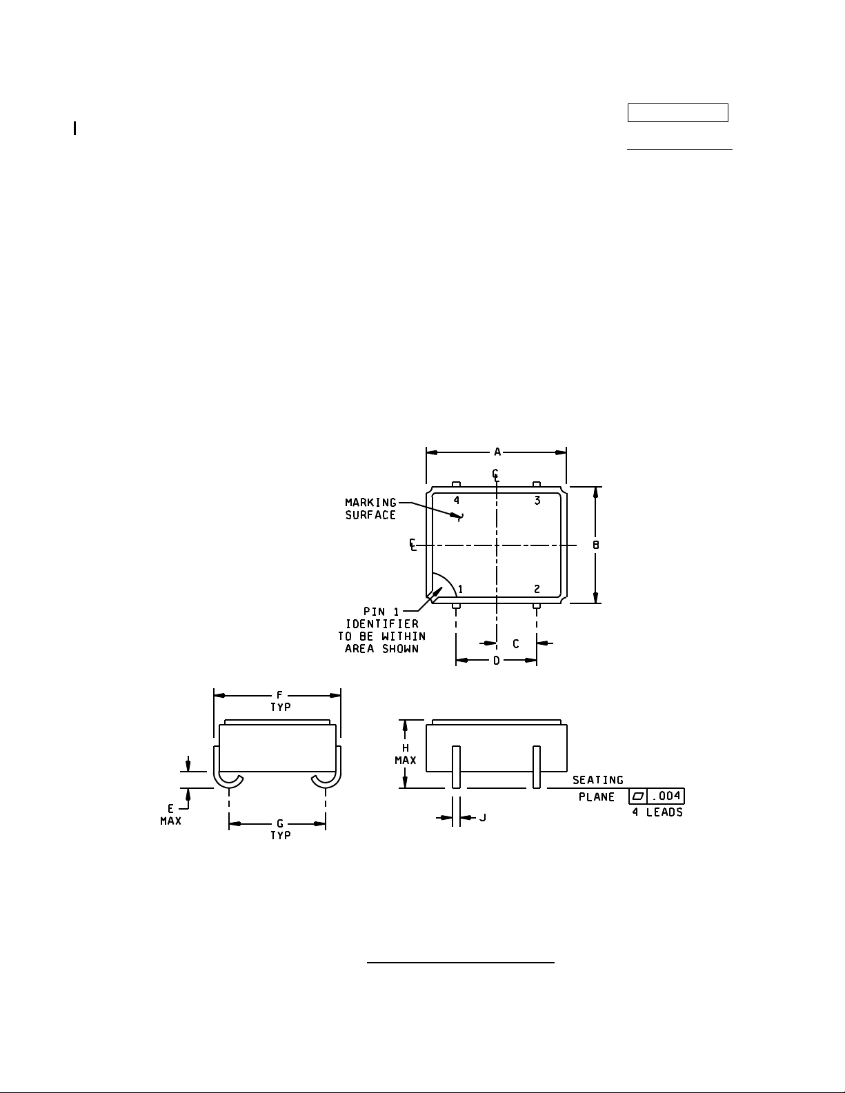
FIGURE 1. Interface and physical dimensions.
AMSC N/A FSC 5955
Page 2
MIL-PRF-55310/34C
Ltr
Inches
mm
Min
Max
Min
Max
A
.345 Typ
.355 Typ
8.76 Typ
9.02 Typ
B
.285 Typ
.295 Typ
7.24 Typ
7.50 Typ
C
.086
.114
2.18
2.90
D
.195
.205
4.95
5.20 E ---
.040
---
1.02 F ---
.320
---
8.13
G
.232
.248
5.89
6.30
H
---
.170
---
4.32
J
.015
.021
0.38
0.53
Pin number
Function
1
Enable/disable
2
GND
3
Output
4
B+
NOTES:
1. Dimensions are in inches.
2. Metric equivalents are given for general information only.
3. Unless otherwise specified, tolerances are ±.005 (0.13 mm) for three place decimals and ±.02 (0.5 mm) for two
place decimals.
FIGURE 1. Interface and physical dimensions - Continued.
2
Page 3

MIL-PRF-55310/34C
REQUIREMENTS:
Interface and physical dimensions: See figure 1.
Mounting: See
Terminals: See
Seal: Hermetic in accordance with MIL-PRF-55310, maximum leakage rate 5 x 10
Weight: 3 grams, maximum.
Oscillator: Class 2 or any class 1 or class 3 oscillator meeting all class 2 requirements and verification tests
specified herein and in MIL-PRF-55310.
Calibration: Manufacturer calibrated.
Screening: In accordance with MIL-PRF-55310, product level B or S, as applicable.
Temperature:
Operating: See
Storage: -62°C to +125°C.
Load test circuit: See figure 2.
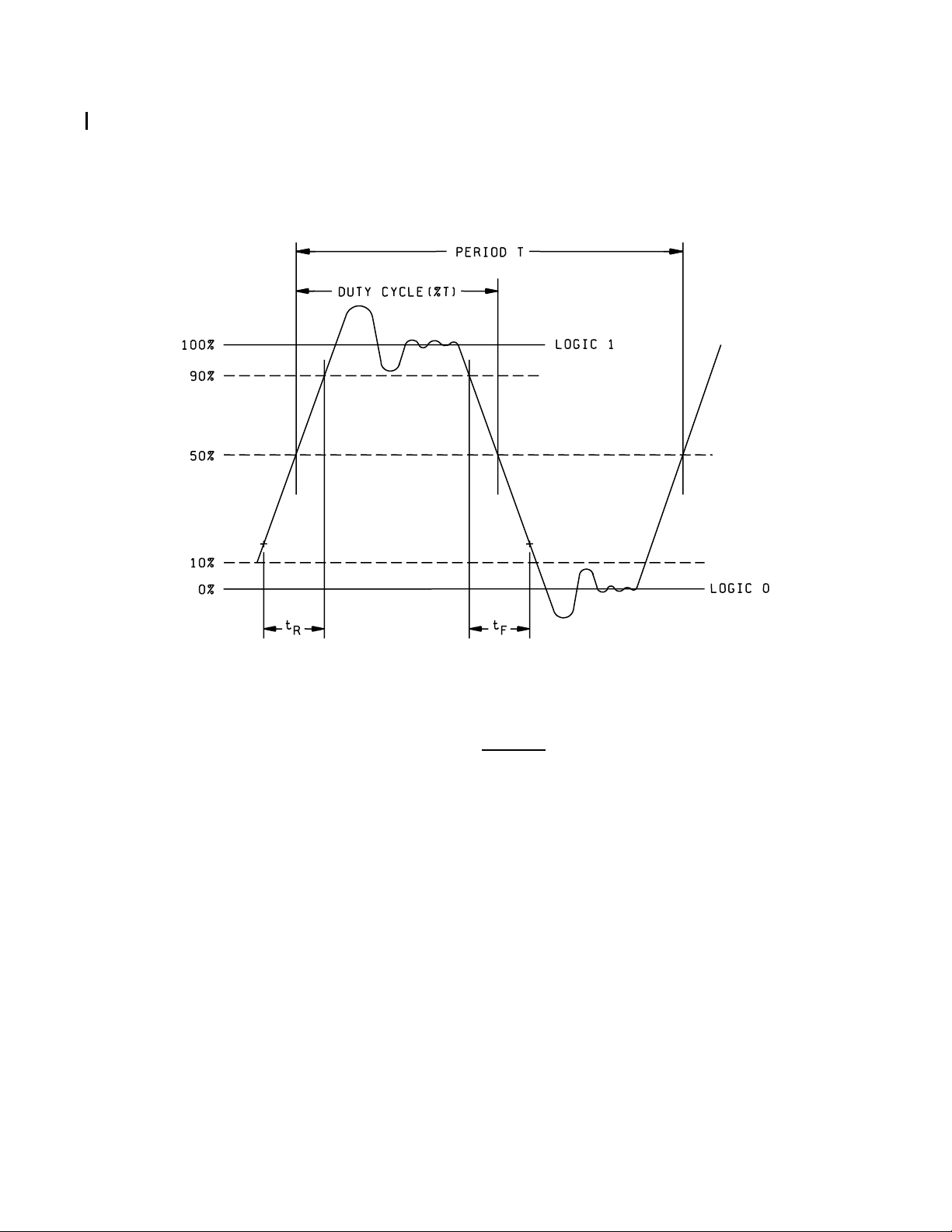
Output waveform: Symmetrical square wave, 3.3 volt CMOS compatible (see
Output logic voltage levels at designated CMOS (see
Logic 1: 90 percent of V
Logic 0: 10 percent of V
Rise and fall times: (See table I) Measurements shall be taken at the 10 percent and 90 percent peak-to
-peak output voltage levels, with peak-to-peak output defined as level 1-level 0 (see
Duty cycle: See
Supply voltage: +3.3 V dc ±10 percent.
Input current: At designated supply voltage (see table I).
Enable/disable:
Output disabled (high impedance): Pin 1 input ≤ 0.3 V dc.
Output active: Pin 1 input ≥ 2.0 V dc or open.
Output frequency: Frequency as designated at time of acquisition (see table I).
Initial accuracy at reference temperature (up to 30 days after shipment): See
figure 1.
figure 1.
table I.
, minimum.
DD
, maximum.
DD
table I and figure 3.
figure 3):
-8
atm cc/s.
figure 3).
figure 3).
table I.
3
Page 4

MIL-PRF-55310/34C
Dash
Output
Input
Pulse characteristics
Initial
Frequency-temperature
tolerance (ppm) 1/
Rise and
Duty cycle
-55°C
+125°C
-55°C
+105°C
-20°C
+55°C
A B C
01
500 kHz to
15.999 MHz
6 mA
6 ns
45% to 55%
±15 ppm
±50
ppm
±40
ppm
±25
ppm
04
500 kHz to
15.999 MHz
6 mA
6 ns
45% to 55%
±25 ppm
±100
ppm
±80
ppm
±50
ppm
11
16.000 MHz to
31.999 MHz
10 mA
5 ns
40% to 60%
±15 ppm
±50
ppm
±40
ppm
±25
ppm
14
16.000 MHz to
31.999 MHz
10 mA
5 ns
40% to 60%
±25 ppm
±100
ppm
±80
ppm
±50
ppm
21
32.000 MHz to
39.999 MHz
15 mA
5 ns
40% to 60%
±15 ppm
±50
ppm
±40
ppm
±25
ppm
24
32.000 MHz to
39.999 MHz
15 mA
5 ns
40% to 60%
±25 ppm
±100
ppm
±80
ppm
±50
ppm
31
40.000 MHz to
64.999 MHz
20 mA
3 ns
40% to 60%
±15 ppm
±50
ppm
±40
ppm
±25
ppm
34
40.000 MHz to
64.999 MHz
20 mA
3 ns
40% to 60%
±25 ppm
±100
ppm
±80
ppm
±50
ppm
41
65.000 MHz to
99.999 MHz
30 mA
3 ns
40% to 60%
±15 ppm
±50
ppm
±40
ppm
±25
ppm
44
65.000 MHz to
99.999 MHz
30 mA
3 ns
40% to 60%
±25 ppm
±100
ppm
±80
ppm
±50
ppm
51
100.00 MHz to
129.999 MHz
40 mA
3 ns
40% to 60%
±15 ppm
±50
ppm
±40
ppm
±25
ppm
54
100.00 MHz to
129.999 MHz
40 mA
3 ns
40% to 60%
±25 ppm
±100
ppm
±80
ppm
±50
ppm
61
130.00 MHz to
150.00 MHz
45 mA
3 ns
40% to 60%
±15 ppm
±50
ppm
±40
ppm
±25
ppm
64
130.00 MHz to
150.00 MHz
45 mA
3 ns
40% to 60%
±25 ppm
±100
ppm
±80
ppm
±50
ppm
TABLE I. Dash numbers and operating characteristics.
number
frequency
range
current
(max) 2/
fall times
(max) 3/
min-max
3/
accuracy
at +23°C
±1°C
to
to
to
1/ Temperature range A applicable for product level B oscillators only.
2/ Maximum input current for no load condition.
3/ See figure 3.
Frequency-temperature tolerance (one-half temperature cycle, referenced to frequency measured at +23°C ±1°C,
immediately prior to starting of the test): See
the specified operating temperature range. 1/
Frequency-voltage tolerance: ±4 ppm maxim
at reference temperature and operating temperature range end points.
1/ For the purpose of transitioning this device to MIL-PRF-55310, ‘Frequency stability versus temperature’ has been
table I. Measurements taken at ten equally spaced increments over
um for a ±10 percent change in supply voltage. Measurements taken
renamed ‘Frequency-temperature tolerance’. The verification requirements of ‘initial frequency-temperature
accuracy (one-half temperature cycle)’ shall apply except that frequency measurements shall be referenced to the
frequency measured at +23°C ±1°C (f
) instead of to the nominal frequency (f
ref
4
nom
).
Page 5

MIL-PRF-55310/34C
Frequency aging: Measurements shall be taken at +70°C ±0.2°C at intervals of not more than every 72 hours for
30 days minimum (Except one maximum interval of 96 hours per 30 days is permitted).
±10 ppm per year, maximum
±1.5 ppm per 30 days.
±3 ppm per 90 days.
Terminal strength: Method 211 of MIL-STD-202, test condition A.
Applied force: 8 ounces each terminal.
Frequency-environmental tolerance: Not applicable.
NOTES:
1. For C
2. For R
3. C
CL
= 15 pF ±5 percent.
CL
= 10 kΩ ±5 percent.
CL
includes scope capacitance.
FIGURE 2. Load test circuit.
5
Page 6
MIL-PRF-55310/34C
FIGURE 3. Waveform
Vibration, sinusoidal: In accordance with MIL-PRF-55310 and method 204 of MIL-STD-202.
Nonoperating: Test condition G.
Operating: Not required.
Ambient pressure:
Nonoperating: In accordance with MIL-PRF-55310.
Operating: Method 105 of MIL-STD-202, test condition C.
Exposure time: 5 minutes.
Reflow soldering: Reflow soldering of the unit at +230°C ±10°C for 15 seconds shall not degrade the performance.
6
Page 7

MIL-PRF-55310/34C
Part or Identifying Number (PIN): Consists of “M” prefix followed by specification sheet number, a dash and coded
alphas, and numeric number. See example:
EXAMPLE
M55310/34- S 01 A XXXXXXXX
M prefix and specification sheet number
Product level (S, B, or C)
Dash number (see table I)
Operating temperature range
(A, B, or C) (see table I)
Frequency
Referenced documents. In addition to MIL-PRF-55310, this document references MIL-STD-202.
The margins of this specification are marked with vertical lines to indicate where changes from the previous issue
were made. This was done as a convenience only and the Government assumes no liability whatsoever for any
inaccuracies in these notations. Bidders and contractors are cautioned to evaluate the requirements of this document
based on the entire content irrespective of the marginal notations and relationship to the last previous issue.
Custodians: Preparing activity:
Army - CR Army - CR
Navy - EC
Air Force - 99 Agent:
DLA - CC DLA - CC
Review activities: (Project 5955-2013-002)
Army - AR, MI, SM
Navy - AS, CG, MC
Air Force - 19, 84
NASA - NA
NOTE: The activities listed above were interested in this document as of the date of this document. Since
organizations and responsibilities can change, you should verify the currency of the information above using the
ASSIST Online database at https://assist.dla.mil.
7
 Loading...