

Page 1
INCH-POUND
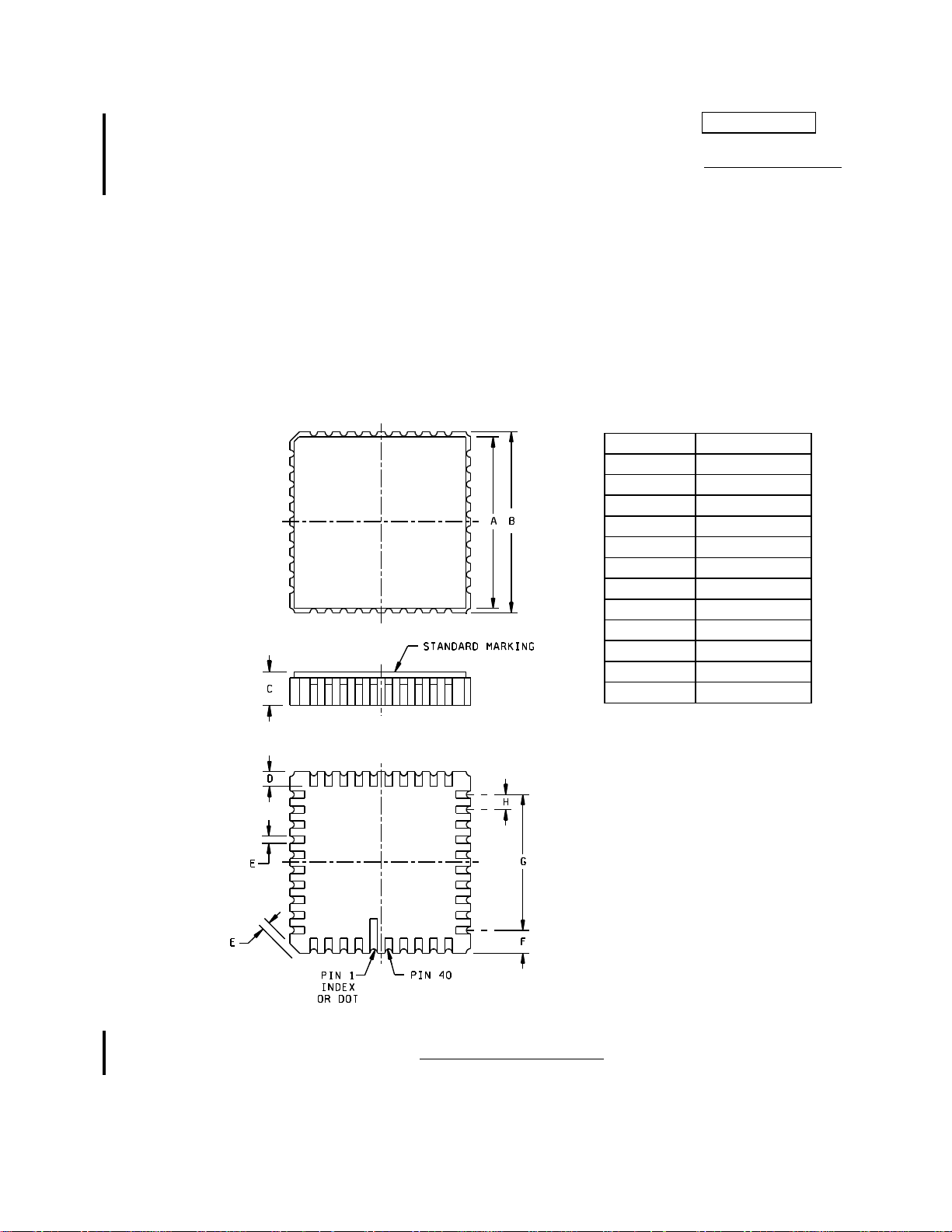
Pin number
Function
4
B+
10
B+
31
GND
32
Disable/enable
39
Output
1-3
NC
11-30
NC
33-36
NC
40
NC
MIL-PRF-55310/29C
25 March 2011
SUPERSEDING
MIL-PRF-55310/29B
24 February 2005
PERFORMANCE SPECIFICATION SHEET
OSCILLATOR, CRYSTAL CONTROLLED, TYPE 1 (CRYSTAL OSCILLATOR (XO)),
0.2 MHz THROUGH 85 MHz, HERMETIC SEAL, SQUARE WAVE, HCMOS
This specification is approved for use by all Departments
and Agencies of the Department of Defense.
The requirements for acquiring the product described herein
shall consist of this specification and MIL-PRF-55310.
37 GND
5-9 NC
38 NC
FIGURE 1. Dimensions and configuration.
AMSC N/A FSC 5955
Page 2
MIL-PRF-55310/29C
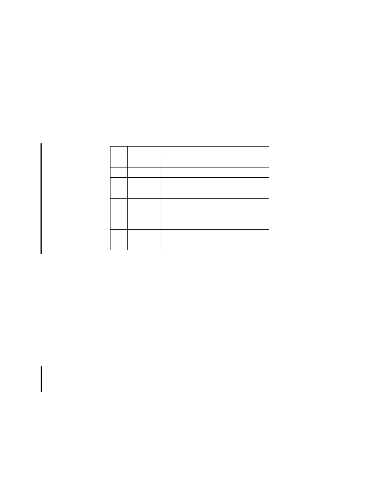
Ltr
Inches
mm
C
---
.085
---
2.16
D
.033
.047
0.84
11.94
E
.015
.025
0.38
0.63
F
.055
.070
1.40
1.78
NOTES:
1. Dimensions are in inches.
2. Metric equivalents are given for general information only.
3. Unless otherwise specified, tolerances are ±.005 (0.13 mm) for three place decimals and ±.02 (0.5 mm) for two
place decimals.
4 All pads with NC functions are not connected externally.
A .454 .466 11.53 11.84
B .465 SQ .495 SQ 11.81 SQ 12.57 SQ
G .355 SQ .365 SQ 9.02 SQ 9.27 SQ
H .035 .045 0.89 1.14
FIGURE 1. Dimensions and configuration - Continued.
Min Max Min Max
2
Page 3

MIL-PRF-55310/29C
REQUIREMENTS:
Interface and physical dimensions: See figure 1.
Mounting: See figure 1.
Pads: See figure 1.
`
Seal: Hermetic in accordance with MIL-PRF-55310, maximum leakage rate 5 x 10
Weight: 3 grams, maximum.
Oscillator: Class 2 or any class 1 or class 3 oscillator meeting all class 2 requirements and verification tests
specified herein and in MIL-PRF-55310.
Calibration: Manufacturer calibrated.
Screening: In accordance with MIL-PRF-55310, product level B or S, as applicable.
Temperature:
Operating: See table I.
Storage: -62°C to +125°C.
Load test circuit: See figure 2.
Supply voltage: +5.0 V dc ±10 percent.
Supply current: See table I.
Overvoltage survivability: In accordance with MIL-PRF-55310.
Start-up time: 15 ms maximum, measurement shall be taken at reference temperature and operating temperature
range end points.
Nominal output frequency: Specified nominal frequency (see table I).
Output levels at designated load: See figure 3.
Logic 1: 0.9 V
, minimum.
DD
Logic 0: 0.1 V
, maximum.
DD
Output waveform: Symmetrical square wave, HCMOS logic compatible (see figure 3).
Duty cycle: See table I and figure 3.
Rise and fall times: See table I and figure 3.
Enable/disable:
Output disabled (high impedance): Pad 32 input = 0.8 V dc maximum.
Output enabled: Pad 32 input = 2.0 V dc minimum.
Initial frequency accuracy at +23°C: See table I.
-8
atm cc/s.
3
Page 4

MIL-PRF-55310/29C
Dash
number
Output
frequency
Input
current
Pulse characteristics
Initial
accuracy
Frequency
aging
Frequency-temperature
tolerance (ppm)
range
(max)
Rise and
Duty Cycle
2/
ppm/year
-55/C
-55/C
-20/C
A B
C
01
0.2 MHz
10 mA
10 ns
45% to 55%
25 ppm
10 ppm
100 ppm
75 ppm
50 ppm
11
5.0 MHz
20 mA
10 ns
45% to 55%
25 ppm
10 ppm
100 ppm
75 ppm
50 ppm
21
25.0 MHz
30 mA
5 ns
45% to 55%
25 ppm
10 ppm
100 ppm
75 ppm
50 ppm
31
40.0 MHz
40 mA
5 ns
40% to 60%
25 ppm
10 ppm
100 ppm
75 ppm
50 ppm
Maximum change over 30 days
0.7 ppm
1.5 ppm
Projected maximum change
for 1 year after 30 days
TABLE I. Dash numbers and operating charact eri sti cs.
1/
to
02
to
12
to
22
to
32
41
to
42
5.0 MHz
25.0 MHz
40.0 MHz
60.0 MHz
60.0 MHz
85.0 MHz
10 mA
20 mA
30 mA
40 mA
60 mA
60 mA
fall times
(max)
10 ns
10 ns
5 ns
5 ns
5 ns
5 ns
min-max
4/
40% to 60%
1/ Maximum input current for no load condition.
2/ Up to 30 days following shipment.
3/ After 30 days following shipment.
4/ See figure 3.
TABLE II. Frequency aging limits.
at +23°C
±1°C
±15 ppm
±
±15 ppm
±
±15 ppm
±
±15 ppm
±25 ppm
±15 ppm
±
(max) 3/
±5 ppm
±
±5 ppm
±
±5 ppm
±
±5 ppm
±10 ppm
±5 ppm
±
to
+125/C
±65 ppm
±
±65 ppm
±
±65 ppm
±
±65 ppm
±100 ppm
±65 ppm
±
+105/C
±55 ppm
±
±55 ppm
±
±55 ppm
±
±55 ppm
±75 ppm
±55 ppm
±
±5 ppm per year 1/ ±10 ppm per year 1/
±
±
±5.0 ppm ±10.0 ppm
to
to
+70/C
±40 ppm
±
±40 ppm
±
±40 ppm
±
±40 ppm
±50 ppm
±40 ppm
±
1/ See table I.
Initial frequency - temperature accuracy (1/2 temperature cycle): See table I. Measurements shall be taken at ten
equally spaced increments over the specified operating temperature range .
Frequency - voltage tolerance for ±10 percent change in supply voltage:
For output frequency ≤ 40.0 MHz: ±2 ppm, maximum.
For output frequency ≥ 40.0 MHz: ±4 ppm, maximum.
Frequency - environmental tolerance: ±3 ppm.
Frequency aging: Frequency aging shall be in accordance with MIL-PRF-55310 and shall meet the limits of
table II.
4
Page 5

MIL-PRF-55310/29C
B
NOTES:
1. For HCMOS: C
2. For HCMOS: R
= 15 pF ±5 percent.
CL
= 10 kΩ ±5 percent.
CL
3. CCL includes scope capacitance.
FIGURE 2. Load test circuit.
FIGURE 3. Waveform.
5
Page 6

MIL-PRF-55310/29C
Vibration, sinusoidal: In accordance with MIL-PRF-55310 and method 204 of MIL-STD-202.
Nonoperating: Test condition D.
Operating: Not required.
Shock, non-operating: Method 213 of MIL-STD-202, condition I.
Thermal shock: Method 107 of MIL-STD-202, condition B.
Ambient pressure:
Nonoperating: In accordance with MIL-PRF-55310.
Operating: Method 105 of MIL-STD-202, test condition C.
Storage temperature: In accordance with MIL-PRF-55310.
Reflow soldering: Reflow soldering of the unit at +230°C ± 10°C for 15 seconds shall not degrade the performance.
Moisture resistance: Method 106 of MIL-STD-202.
Pad strength: In accordance with method 2004 of MIL-STD-883, condition D.
Solderability: Method 208 of MIL-STD-202.
Resistance to solvents: Method 215 of MIL-STD-202.
Screening: In accordance with MIL-PRF-55310, class B or S, as applicable.
Part or Identifying Number (PIN): Consists of “M” prefix followed by specification sheet number, a dash and coded
alphas, and numeric number. See example:
EXAMPLE
M55310/29- S 01 A XXXXXXXX
M prefix and specification sheet number
Product level (S, B, or C)
Dash number (see table I)
Operating temperature range
(A, B, or C) (see table I)
Frequency
6
Page 7

MIL-PRF-55310/29C
Reference documents. In addition to MIL-PRF-55310, this document references the following:
MIL-STD-202
MIL-STD-883
The margins of this specification sheet are mark ed with ver ti cal lin es to indicate where changes from the previous
issue were made. This was done as a convenience only and the Government assumes no liability whatsoever for
any inaccuracies in these notations. Bidders and contractors are cautioned to evaluate the requirements of this
document based on the entire content irrespective of the marginal notations and relationship to the last previous
issue.
Custodians: Preparing activity:
Army - CR Army - CR
Navy - EC
Air Force - 99 Agent:
DLA - CC DLA - CC
Review activities:
Army - AR, MI, SM (5955-2011-016)
Navy - AS, CG, MC
Air Force - 19, 84
NASA - NA
NOTE: The activities listed above were interested in this document as of the date of this document. Since
organizations and responsibilities can change, you should verify the currency of the information above using the
ASSIST Online database at
https://assist.daps.dla.mil.
7
 Loading...