

USB0403
thru
USB0424C
LOW CAPACITANCE TVS ARRAY
105205.R1 6/06 www.protekdevices.com
APPLICATIONS
✔ Ethernet - 10/100 Base T
✔ Cellular Phones
✔ Audio & Video Inputs
✔ FireWire, SCSI & USB Interfaces
IEC COMPATIBILITY (EN61000-4)
✔ 61000-4-2 (ESD): Air - 15kV, Contact - 8kV
✔ 61000-4-4 (EFT): 40A - 5/50ns
✔ 61000-4-5 (Surge): 12A, 8/20µs - Level 1(Line-Gnd) & Level 2(Line-Line)
FEATURES
✔ 500 Watts Peak Pulse Power per Line (tp=8/20µs)
✔ Unidirectional & Bidirectional Configurations
✔ Available in Multiple Voltage Types Ranging From 3V to 24V
✔ Protects One Line
✔ ESD Protection > 40 kilovolts
✔ Low Leakage
✔ Low Capacitance: 5pF per Line Pair
✔ RoHS Compliant in Lead-Free Versions
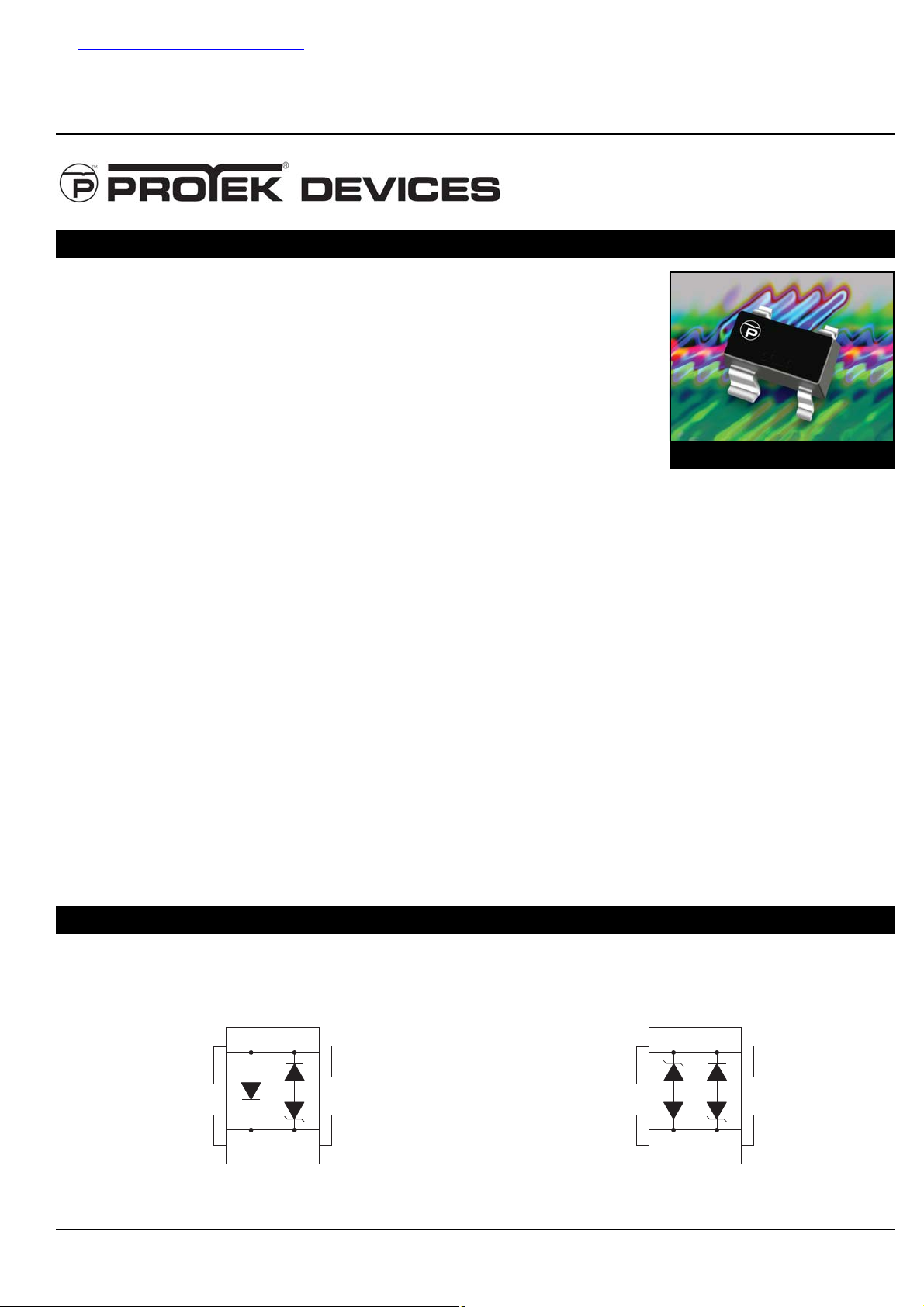
MECHANICAL CHARACTERISTICS
✔ Molded JEDEC SOT-143 Package
✔ Weight 9 milligrams (Approximate)
✔ Available in Tin-Lead or Lead-Free Pure-Tin Plating(Annealed)
✔ Solder Reflow Temperature:
Tin-Lead - Sn/Pb, 85/15: 240-245°C
Pure-Tin - Sn, 100: 260-270°C
✔ Flammability Rating UL 94V-0
✔ 8mm Tape and Reel Per EIA Standard 481
✔ Marking: Marking Code
05205
PIN CONFIGURATIONS
3
4
1
2
UNIDIRECTIONAL BIDIRECTIONAL
3
4
1
2
SOT-143
查询USB0415C-LF-T7供应商

USB0403
thru
USB0424C
205205.R1 6/06 www.protekdevices.com
DEVICE CHARACTERISTICS
Operating Temperature
SYMBOL VALUE
-55°C to 150°C °C
°C-55°C to 150°C
UNITS
T
J
T
STG
PARAMETER
Storage Temperature
Peak Pulse Power (tp = 8/20µs) - See Figure 1
P
PP
500 Watts
MAXIMUM RATINGS @ 25°C Unless Otherwise Specified
Note 1: Part numbers with an additional “C” suffix are bidirectional devices, i.e., USB0405C.
Note 2:
Unidirectional Only:
Positive potential is applied from pin 2 to 1 or pin 3 to 4.
PA RT
NUMBER
(See Notes 1-2)
DEVICE
MARKING
MINIMUM
BREAKDOWN
VOLTAGE
@ 1mA
V
(BR)
VOLTS
MAXIMUM
CLAMPING
VOLTAGE
(See Fig. 2)
@ IP = 5A
V
C
VOLTS
MAXIMUM
CLAMPING
VOLTAGE
(See Fig. 2)
@8/20µs
VC @ I
PP
MAXIMUM
CAPACITANCE
0V @ 1 MHz
C
pF
USB0403
USB0403C
USB0405
USB0405C
USB0408
USB0408C
USB0412
USB0412C
USB0415
USB0415C
USB0424
USB0424C
3U
3B
5U
5B
8U
8B
12U
12B
15U
15B
24U
24B
4.0
4.0
6.0
6.0
8.5
8.5
13.3
13.3
16.6
16.6
26.7
26.7
9.0
9.0
11.0
11.0
16.6
16.6
24.0
24.0
30.0
30.0
N/A
N/A
19.0V @ 20.0A
19.0V @ 20.0A
18.3V @ 17.0A
18.3V @ 17.0A
18.5V @ 17.0A
18.5V @ 17.0A
28.6V @ 11.0A
28.6V @ 11.0A
31.8V @ 10.0A
31.8V @ 10.0A
56.0V @ 6.0A
56.0V @ 6.0A
5
5
5
5
5
5
5
5
5
5
5
5
MAXIMUM
LEAKAGE
CURRENT
@V
WM
I
D
µA
125
125
20
20
10
10
1
1
1
1
1
1
RATED
STAND-OFF
VOLTAGE
V
WM
VOLTS
3.3
3.3
5.0
5.0
8.0
8.0
12.0
12.0
15.0
15.0
24.0
24.0
ELECTRICAL CHARACTERISTICS PER LINE @ 25°C Unless Otherwise Specified
0 5 10 15 20 25 30
t - Time - µs
0
20
40
60
80
100
120
I
PP
- Peak Pulse Current - % of I
PP
TEST
WAVEFORM
PARAMETERS
tf = 8µs
td = 20µs
t
f
Peak Value I
PP
e
-t
td = t
IPP/2
FIGURE 2
PULSE WAVE FORM
0.1 1 10 100 1,000 10,000
td - Pulse Duration - µs
500W 8/20µs Waveform
10
100
1,000
10,000
P
PP
- Peak Pulse Power - Watts
FIGURE 1
PEAK PULSE POWER VS PULSE TIME
USB0403
thru
USB0424C
305205.R1 6/06 www.protekdevices.com
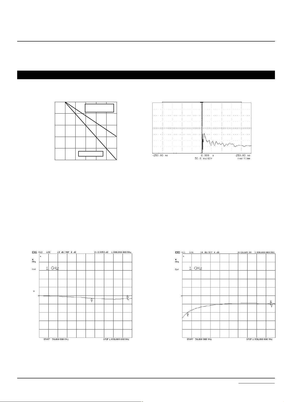
FIGURE 6
RETURN LOSS - USB0405C
100 MHz per Division
10 db per Division
-50 db
-20 db
Ref 0 db
20 db
FIGURE 5
INSERTION LOSS - USB0405C
100 MHz per Division
10 db per Division
-50 db
-20 db
Ref 0 db
20 db
GRAPHS
0 25 50 75 100 125 150
TL - Lead Temperature - °C
20
40
60
80
100
% Of Rated Power
Peak Pulse Power
8/20µs
Average Power
FIGURE 3
POWER DERATING CURVE
0
FIGURE 4
OVERSHOOT & CLAMPING VOLTAGE FOR USB0405C
ESD Test Pulse: 5 kilovolt, 1/30ns (waveform)
5 Volts per Division
0
10
20
30
40

USB0403
thru
USB0424C
405205.R1 6/06 www.protekdevices.com
CIRCUIT BOARD LAYOUT RECOMMENDATIONS
Circuit board layout is critical for Electromagnetic Compatibility
(EMC) protection. The following guidelines are recommended:
✔ The protection device should be placed near the input
terminals or connectors, the device will divert the transient
current immediately before it can be coupled into the nearby
traces.
✔ The path length between the TVS device and the protected
line should be minimized.
✔ All conductive loops including power and ground loops
should be minimized.
✔ The transient current return path to ground should be kept
as short as possible to reduce parasitic inductance.
✔ Ground planes should be used whenever possible. For
multilayer PCBs, use ground vias.
The USB04 Series are TVS arrays designed to protect I/O or
data lines from the damaging effects of ESD and EFT. This
product series provides both unidirectional and bidirectional
protection, with a surge capability of 500 Watts PPP per line for
an 8/20µs waveform and ESD protection > 40kV.
UNIDIRECTIONAL
COMMON-MODE CONFIGURATION (Figure 1)
The two USB04 Series devices provide protection in a commonmode configuration as depicted in Figure 1.
Circuit connectivity is as follows:
✔ TVS Device 1: Line 1(D+) is connected to Pins 2 & 3.
✔ TVS Device 2: Line 2(D-) is connected to Pins 2 & 3.
✔ Both TVS Devices: Pins 1 & 4 connected to ground.
BIDIRECTIONAL
DIFFERENTIAL-MODE CONFIGURATION (Figure 2)
The USB04xxC Series provides protection in a differential-mode
configuration as depicted in Figure 2.
Circuit connectivity is as follows:
✔ Line 1(RX) is connected to Pins 1 & 4.
✔ Line 2(TX) is connected to Pins 2 & 3.
Figure 1 - Unidirectional Configuration (Two TVS Devices)
Common-Mode USB Protection
;;;;;;;;;;;;;;;;;;;;;;;;;;;;;;;;;;;;;;;;;;;;
;
;;;;;;;;;;;;;;;;;;;;;;;;;;;;;;;;;;;;;;;;;;;;
;
;;;;;;;;;;;;;;;;;;;;;;;;;;;;;;;;;;;;;;;;;;;;
;
;;;;;;;;;;;;;;;;;;;;;;;;;;;;;;;;;;;;;;;;;;;;
;
;;;;;;;;;;;;;;;;;;;;;;;;;;;;;;;;;;;;;;;;;;;;
;
1 4
32
1 4
2 3
D+
USB IC
D-
USB OUTPUT CONNECTOR
GND
SOLDER PAD
Figure 2 - Bidirectional Configuration
Differential-Mode Ethernet Protection
1 4
32
R
R
T
X
RJ-45
R
X
ETHERNET TRANSCEIVER
APPLICATIONS

USB0403
thru
USB0424C
505205.R1 6/06 www.protekdevices.com
SOT-143 PACKAGE OUTLINE & DIMENSIONS
TAPE & REEL ORDERING NOMENCLATURE
1. Surface mount product is taped and reeled in accordance with EIA-481.
2. Suffix-T7 = 7 Inch Reel - 3,000 pieces per 8mm tape, i.e.,
USB0405C-T7.
3. Suffix-T13 = 13 Inch Reel - 10,000 pieces per 8mm tape,
i.e.,
USB0405C-T13.
4. Suffix - LF = Lead-Free, Pure-Tin Plating, i.e.,
USB0405C-LF-T7.
A
B
C
D
F
G
H
J
K
L
R
S
2.80
1.20
0.84
0.39
0.79
1.78
0.013
0.08
0.46
0.445
0.72
2.11
3.04
1.39
1.14
0.50
0.93
2.03
0.10
0.15
0.60
0.60
0.83
2.48
0.110
0.047
0.033
0.015
0.031
0.070
0.0005
0.003
0.018
0.0175
0.028
0.083
0.120
0.055
0.045
0.020
0.037
0.080
0.004
0.006
0.024
0.024
0.033
0.098
DIM MIN MAX MIN MAX
MILLIMETERS
INCHES
PACKAGE DIMENSIONS
NOTES
1. Dimensioning and tolerances per ANSI Y14.5M, 1985.
2. Controlling Dimension: Inches
3. Dimensions are exclusive of mold flash and metal burrs.
PACKAGE OUTLINE
SOT-143
MOUNTING PAD
A
G
L
B
S
F
D
K
J
C
R
H
0.112
0.079
0.071
0.075
0.041
0.108
0.047
0.031
0.033
0.033
0.033
1
2
3
4
5
6
7
8
9
10
11
2.85
2.00
1.80
1.90
1.05
2.75
1.20
0.80
0.85
0.85
0.85
DIM
Millimeters Inches
TYPICAL
1
2
4
3
5
6
798
10
11
Top cover tape
K0
t
D
P0
P2
10 Pitches Cumulative
Tolerance on Tape. ± 0.2
A0
B0
P
E
F
W
User Direction of Feed
Tape & Reel Specifications (Dimensions in millimeters)
D E P0 tmaxFP2W
1.50 ± 0.10 1.75 ± 0.10 3.50 ± 0.05 8.00 ±0.30 4.00 ±0.10 2.00 ±0.05P4.00 ±0.10 0.25
A0 B0 K0Reel Dia. Tape Width
178mm (7”) 8mm 3.10 ± 0.10 2.70 ± 0.10 1.35 ± 0.10
COPYRIGHT © ProTek Devices 2003
SPECIFICATIONS: ProTek reserves the right to change the electrical and or mechanical characteristics described herein without notice (except JEDEC).
DESIGN CHANGES: ProTek reserves the right to discontinue product lines without notice, and that the final judgement concerning selection and specifications is
the buyer’s and that in furnishing engineering and technical assistance, ProTek assumes no responsibility with respect to the selection or specifications of such
products.
Outline & Dimensions: Rev 2 - 6/06, 06011
ProTek Devices
2929 South Fair Lane, Tempe, AZ 85282
Tel: 602-431-8101 Fax: 602-431-2288
E-Mail: sales@protekdevices.com
Web Site: www.protekdevices.com
 Loading...