

Protekdevices EMC8.0F-LC, EMC5.0F-LC, EMC3.3F-LC, EMC15F-LC, EMC12F-LC Datasheet
1
www.protekdevices.com05087.R1 1/03
EMC3.3F-LC
thru
EMC15F-LC
TVS/LOW PASS L/C FILTER ARRAYS
APPLICATIONS
✔ High-Speed Networks
✔ Graphics/Video Cards
✔ Global Positioning Systems
✔ Wireless Networks
IEC COMPATIBILITY (EN61000-4)
✔ 61000-4-2 (ESD): Air - 15kV, Contact - 8kV
✔ 61000-4-4 (EFT): 40A - 5/50ns
FEATURES
✔ 300 Watts Peak Pulse Power per Line (tp=8/20µs)
✔ EMI/RFI Low Pass Filtering
✔ Very Low Insertion Loss: < 0.5dB up to 200 MHz
✔ Excellent Matching Over the Operating Frequency
✔ Protects 3.3 - 15 Volt I/O Ports
✔ 50 Ohm Network Terminations
✔ L/C Bessel Filter
✔ ✔
✔ ✔
✔
LOW CAPACITANCE: 10pF
MECHANICAL CHARACTERISTICS
✔ Molded JEDEC SO-16WB (Wide Body) Package
✔ Weight 0.15 grams (Approximate)
✔ Flammability rating UL 94V-0
✔ 16mm Tape and Reel Per EIA Standard 481
✔ Marking: Logo, Part Number & Pin One Defined By Dot on Top of Package
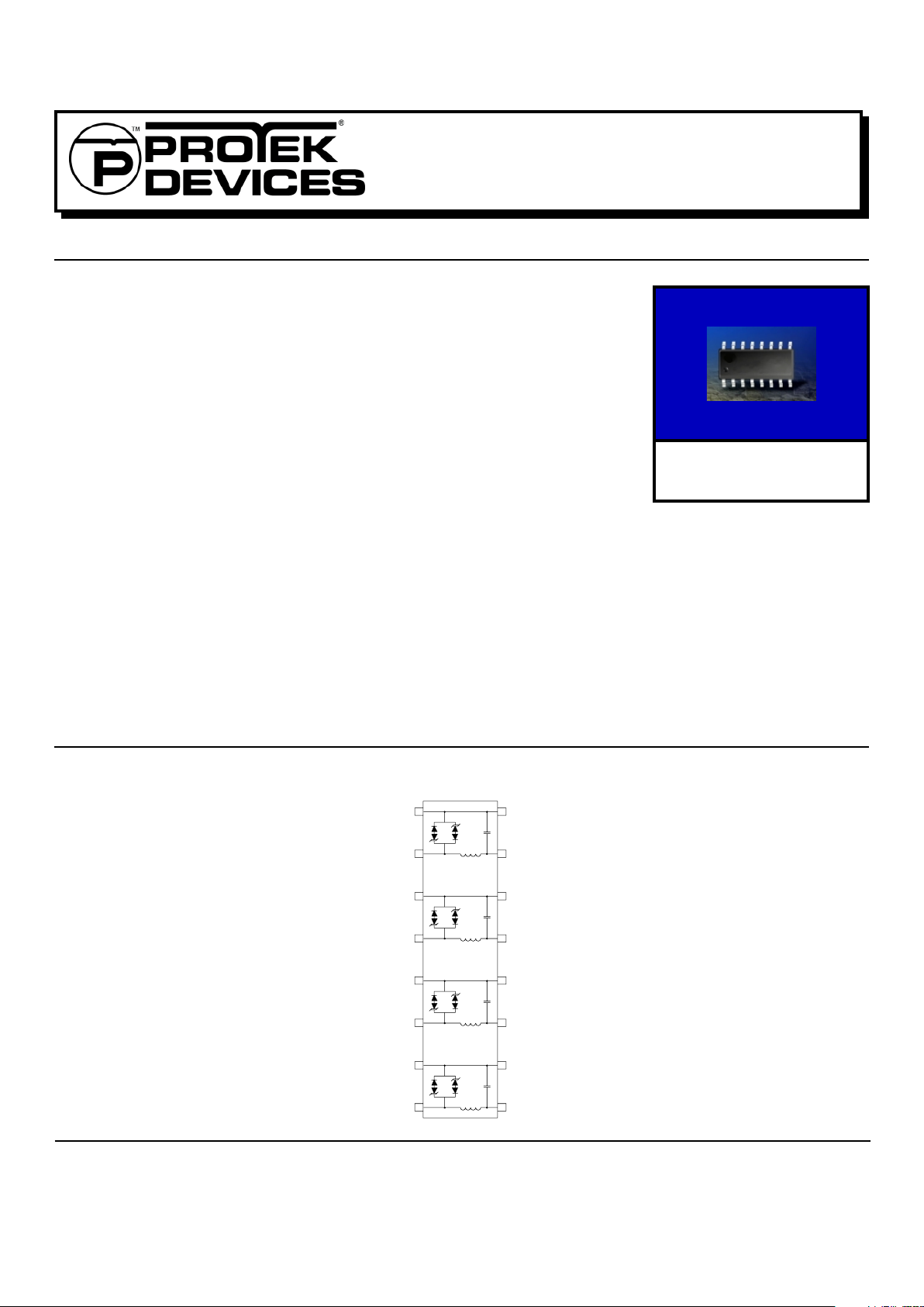
CIRCUIT DIAGRAM
SO-16WB
(Wide Body)
05087
. . . engineered solutions for the transient environment™
1
16
15
14
13
12
11
10
9
2
3
4
5
6
7
8
GND
GND
GND
GND
GND
GND
GND
GND
OUT
OUT
OUT
OUT
IN
IN
IN
IN

2 www.protekdevices.com
EMC3.3F-LC
thru
EMC15F-LC
05087.R1 1/03
DEVICE CHARACTERISTICS
MAXIMUM RATINGS @ 25°C Unless Otherwise Specified
Operating Temperature
SYMBOL VALUE
-55°C to 150°C
°C
°C
-55°C to 150°C
UNITS
T
J
T
STG
PARAMETER
Storage Temperature
Peak Pulse Power (tp = 8/20µs) - See Figure 1
P
PP
300 Watts
ELECTRICAL CHARACTERISTICS PER LINE @ 25°C Unless Otherwise Specified
PA RT
NUMBER
MAXIMUM
OPERATING
VOLTAGE
V
(OP)
VOLTS
MINIMUM
BREAKDOWN
VOLTAGE
(See Note 1)
@ 1mA
V
(BR)
VOLTS
MAXIMUM
CLAMPING
VOLTAGE
(See Fig. 5)
@ IPP = 5A
V
C
VOLTS
CUT-OFF
FREQUENCY
@ -3dB
f
c
MHz
EMC3.3F-LC
EMC5.0F-LC
EMC8.0F-LC
EMC12F-LC
EMC15F-LC
3.3
5.0
8.0
12.0
15.0
4.0
6.0
8.5
13.3
16.7
100
50
5
5
5
9.0
11.0
16.6
24.0
30.0
MAXIMUM
LEAKAGE
CURRENT
(See Note 1)
@V
WM
I
D
µA
TYPICAL
CAPACITANCE
(See Note 2)
@ 0V, 1 MHz
C
pF
10
10
10
10
10
500
500
500
500
500
Note 1: Apply positive (negative) potential between input pins to ground pins, output open.
Note 2: Measure capacitance between output pins to ground pins.
 Loading...