

Power Integrations TOP104YAI, TOP103YAI, TOP102YAI, TOP101YAI, TOP100YAI Datasheet
July 1996
Product Highlights
Low Cost Replacement for Discrete Switchers
• 20 to 50 fewer components - cuts cost, increases reliability
• Source-connected tab and Controlled MOSFET turn-on
reduce EMI and EMI filter costs
• Allows for a 50% smaller and lighter solution
• Cost competitive with linears above 5 W
Up to 90% Efficiency in Flyback Topology
• Built-in start-up and current limit reduce DC losses
• Low capacitance 350 V MOSFET cuts AC losses
• CMOS controller/gate driver consumes only 6 mW
• 70% maximum duty cycle minimizes conduction losses
Simplifies Design - Reduces Time to Market
• Supported by many reference designs
• Integrated PWM Controller and 350 V MOSFET in a
industry standard three pin TO-220 package
• Only one external capacitor needed for compensation,
bypass and start-up/auto-restart functions
System Level Fault Protection Features
• Auto-restart and cycle by cycle current limiting functions
handle both primary and secondary faults
• On-chip latching thermal shutdown protects the entire
system against overload
Highly Versatile
• Implements Buck, Boost, Flyback or Forward topology
• Easily interfaces with both opto and primary feedback
• Supports continuous or discontinuous mode of operation
• Specified for operation down to 16 V DC input
Description
The TOPSwitch family implements, with only three pins, all
functions necessary for an off-line switched mode control
system: high voltage N-channel power MOSFET with controlled
turn-on gate driver, voltage mode PWM controller with
integrated 100 kHz oscillator, high voltage start-up bias circuit,
bandgap derived reference, bias shunt regulator/error amplifier
for loop compensation and fault protection circuitry. Compared
to discrete MOSFET and controller or self oscillating (RCC)
switching converter solutions, a TOPSwitch integrated circuit
can reduce total cost, component count, size, weight and at the
same time increase efficiency and system reliability. These
®
PI-1704112995
AC
IN
DRAIN
SOURCE
CONTROL
TOPSwitch
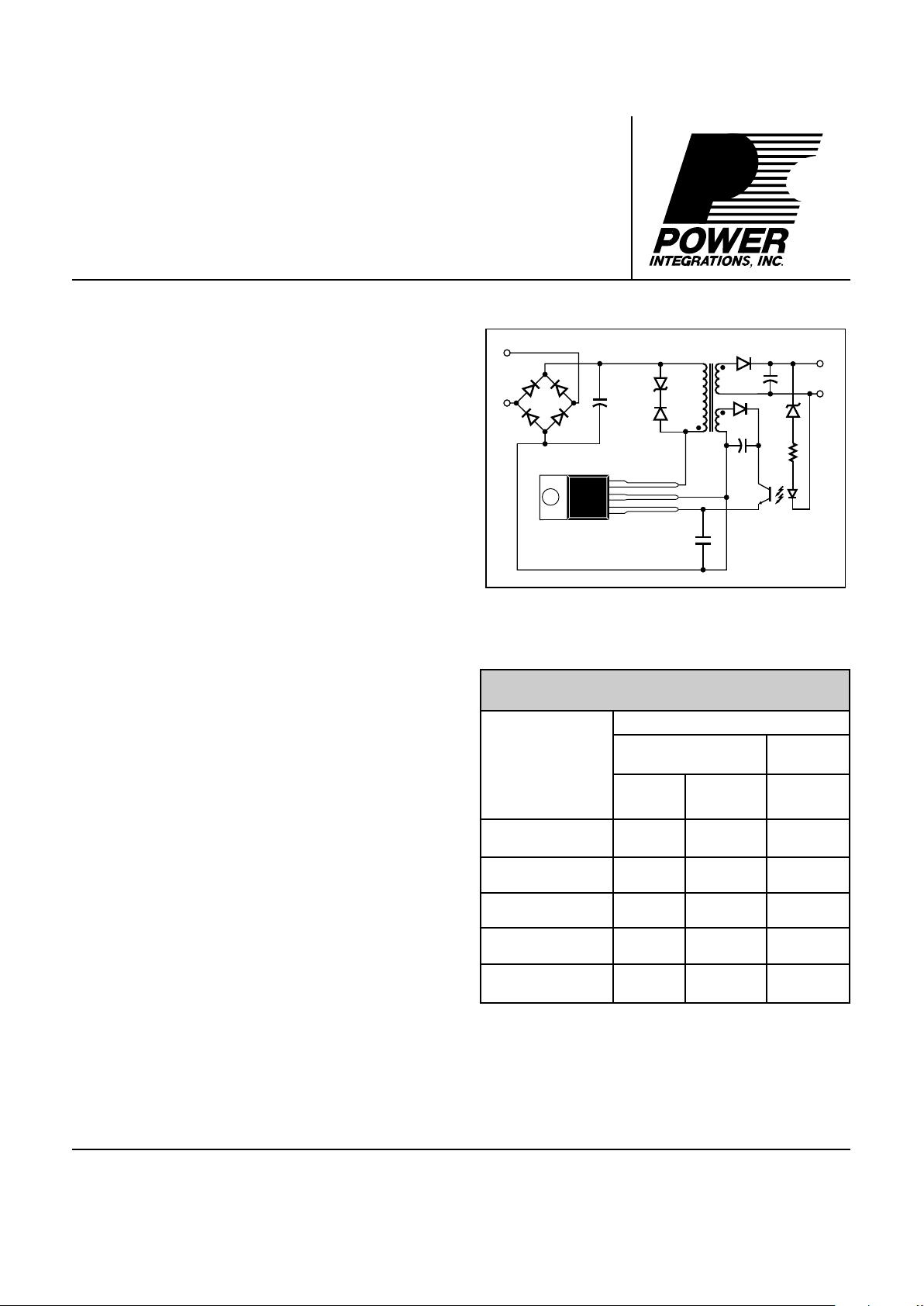
Figure 1. Typical Application.
TOP100-4
TOPSwitch
Family
Three-terminal Off-line PWM Switch
ORDER
PART
NUMBER
OUTPUT POWER RANGE
TOPSwitch
SELECTION GUIDE
FLYBACK
TOP100YAI* 0-20 W 0-30 W
TOP101YAI* 15-35 W 25-50 W
TOP102YAI* 20-45 W 35-70 W
TOP103YAI* 25-55 W 45-90 W
TOP104YAI* 30-60 W 55-110 W
®
* Package Outline: Y03A
devices are intended for 100/110 VAC off-line Power Supply
applications in the 0 to 60 W range and power factor correction
(PFC) applications in the 0 to 110 W range. They are also well
suited for Telecom, Cablecom and other DC to DC converter
applications in the 0-25 W range (see Design Note DN-16).
100/110 V
VAC
0-6.8 W
6-12 W
8.5-17 W
11-22 W
12-25 W
PFC/
BOOST
100/110
VAC
48 V
DC
E
7/96
2
TOP100-4
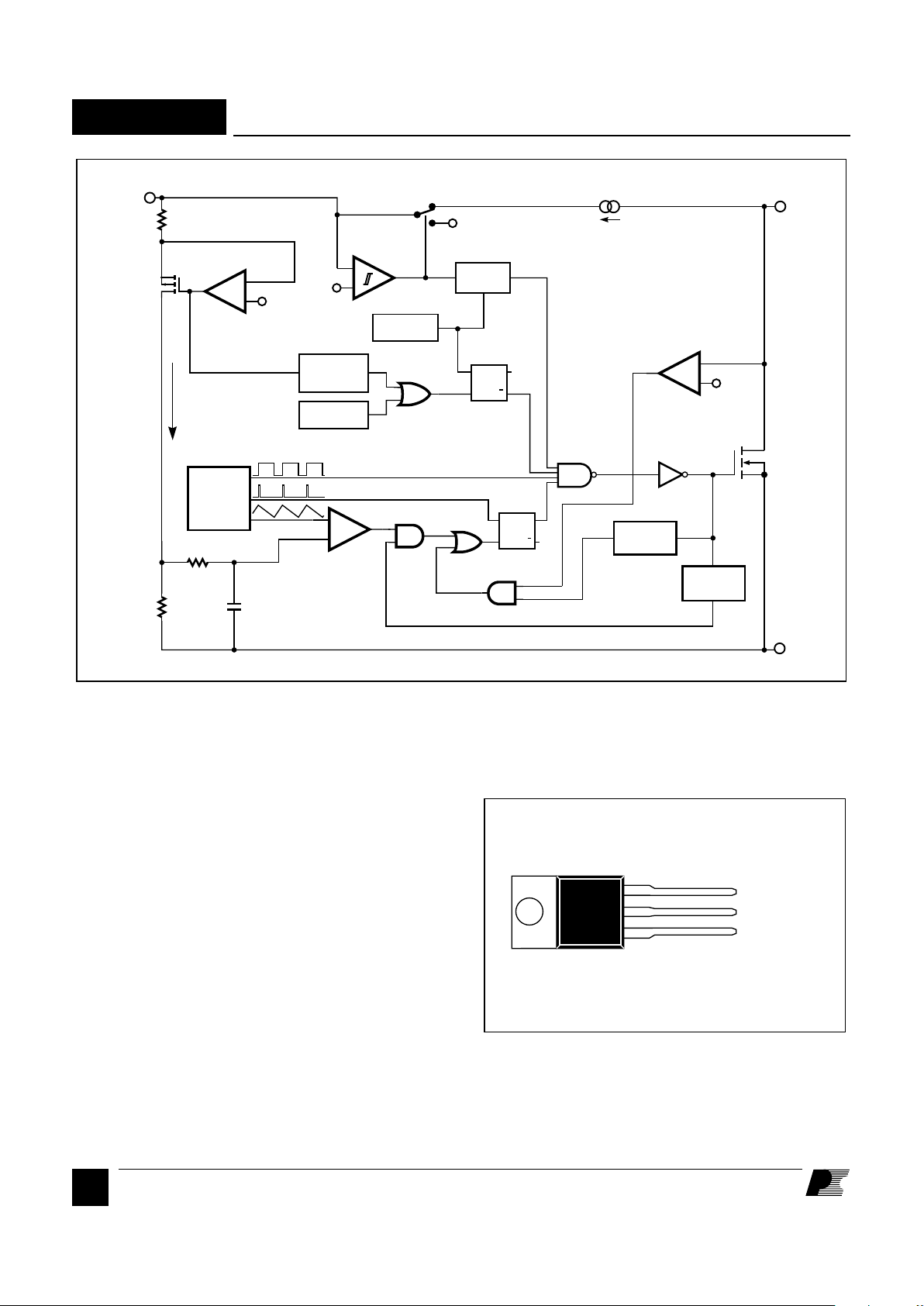
PI-1746-011796
SHUTDOWN/
AUTO-RESTART
PWM
COMPARATOR
CLOCK
SAW
OSCILLATOR
CONTROLLED
TURN-ON
GATE
DRIVER
INTERNAL
SUPPLY
5.7 V
4.7 V
SOURCE
SRQ
Q
D
MAX
+
CONTROL
+
5.7 V
I
FB
R
E
Z
C
V
C
MINIMUM
ON-TIME
DELAY
+
-
V
I
LIMIT
LEADING
EDGE
BLANKING
POWER-UP
RESET
RSQ
Q
÷ 8
0
1
THERMAL
SHUTDOWN
EXTERNALLY
TRIGGERED
SHUTDOWN
SHUNT REGULATOR/
ERROR AMPLIFIER
+
-
DRAIN
Figure 2. Functional Block Diagram.
Pin Functional Description
DRAIN Pin:
Output MOSFET drain connection. Provides internal bias
current during start-up operation via an internal switched highvoltage current source. Internal current sense point.
CONTROL Pin:
Error amplifier and feedback current input pin for duty cycle
control. Internal shunt regulator connection to provide internal
bias current during normal operation. Trigger input for latching
shutdown. It is also used as the supply bypass and auto-restart/
compensation capacitor connection point.
SOURCE Pin:
Output MOSFET source connection. Primary-side circuit
common, power return, and reference point.
PI-1065A-110194
CONTROL
DRAIN
SOURCE (TAB)
TO-220/3 (YO3A)
Figure 3. Pin Configuration.
E
7/96
TOP100-4
3
TOPSwitch
Family Functional Description
TOPSwitch is a self biased and protected
linear control current-to-duty cycle
converter with an open drain output.
High efficiency is achieved through the
use of CMOS and integration of the
maximum number of functions possible.
CMOS significantly reduces bias
currents as compared to bipolar or
discrete solutions. Integration eliminates
external power resistors used for current
sensing and/or supplying initial start-up
bias current.
During normal operation, the internal
output MOSFET duty cycle linearly
decreases with increasing CONTROL
pin current as shown in Figure 4. To
implement all the required control, bias,
and protection functions, the DRAIN
and CONTROL pins each perform
several functions as described below.
Refer to Figure 2 for a block diagram
and Figure 6 for timing and voltage
waveforms of the TOPSwitch integrated
circuit.
Control Voltage Supply
CONTROL pin voltage VC is the supply
or bias voltage for the controller and
driver circuitry. An external bypass
capacitor closely connected between the
CONTROL and SOURCE pins is
required to supply the gate drive current.
The total amount of capacitance
connected to this pin (CT) also sets the
auto-restart timing as well as control
loop compensation. VC is regulated in
either of two modes of operation.
Hysteretic regulation is used for initial
start-up and overload operation. Shunt
regulation is used to separate the duty
cycle error signal from the control circuit
supply current. During start-up, V
C
current is supplied from a high-voltage
switched current source connected
internally between the DRAIN and
CONTROL pins. The current source
provides sufficient current to supply the
control circuitry as well as charge the
total external capacitance (CT).
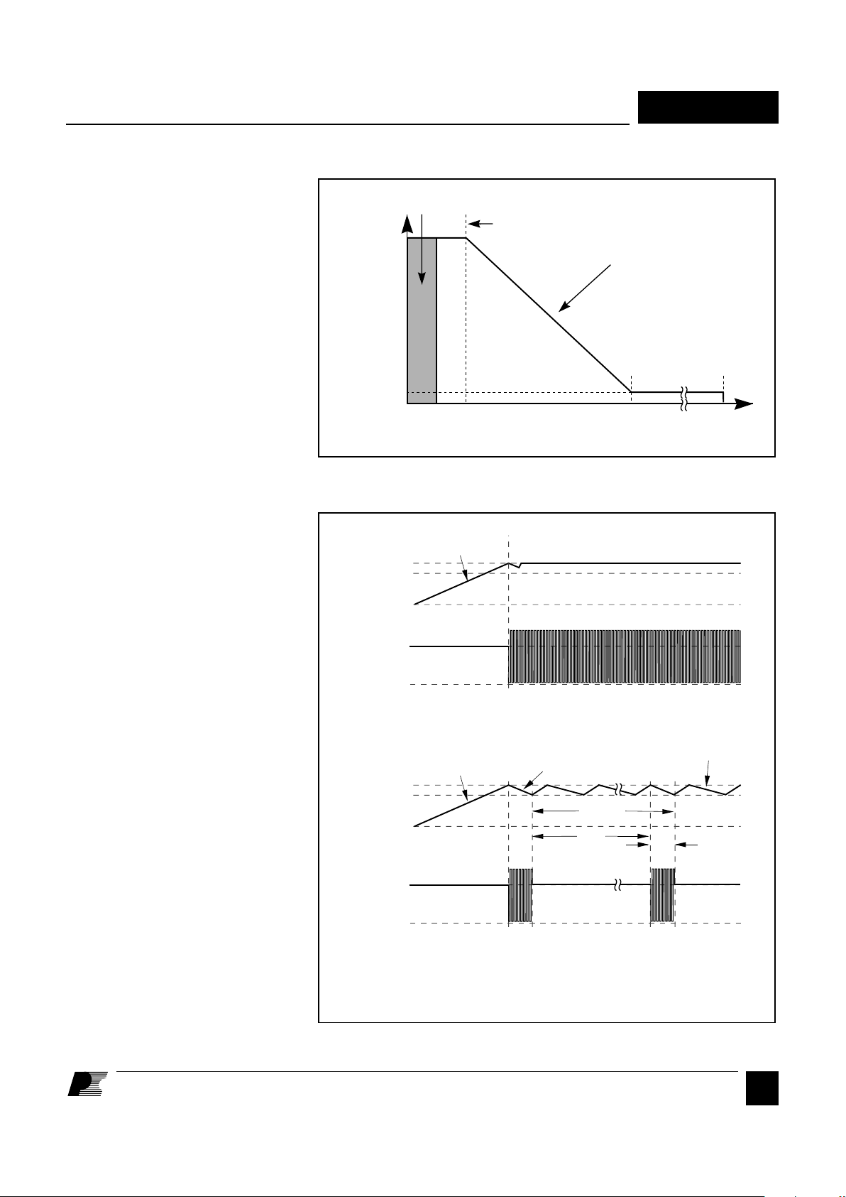
PI-1691-112895
D
MAX
D
MIN
I
CD1
Duty Cycle (%)
IC (mA)
2.5 6.5 45
Slope = PWM Gain
-16%/mA
I
B
Auto-restart
Figure 4. Relationship of Duty Cycle to CONTROL Pin Current.
Figure 5. Start-up Waveforms for (a) Normal Operation and (b) Auto-restart.
DRAIN
0
V
IN
V
C
0
4.7 V
5.7 V
8 Cycles
95%
5%
Off
Switching Switching
Off
IC
Charging C
T
I
CD1
Discharging C
T
I
CD2
Discharging C
T
IC
Charging C
T
Off
PI-1124A-060694
DRAIN
0
V
IN
V
C
0
4.7 V
5.7 V
Off
Switching
(b)
(a)
CT is the total external capacitance
connected to the CONTROL pin

E
7/96
4
TOP100-4
The first time VC reaches the upper
threshold, the high-voltage current
source is turned off and the PWM
modulator and output transistor are
activated, as shown in Figure 5(a).
During normal operation (when the
output voltage is regulated) feedback
control current supplies the VC supply
current. The shunt regulator keeps VC at
typically 5.7 V by shunting CONTROL
pin feedback current exceeding the
required DC supply current through the
PWM error signal sense resistor RE. The
low dynamic impedance of this pin (ZC)
sets the gain of the error amplifier when
used in a primary feedback
configuration. The dynamic impedance
of the CONTROL pin together with the
external resistance and capacitance
determines the control loop
compensation of the power system.
If the CONTROL pin external
capacitance (CT) should discharge to the
lower threshold, then the output
MOSFET is turned off and the control
circuit is placed in a low-current standby
mode. The high-voltage current source
is turned on and charges the external
capacitance again. Charging current is
shown with a negative polarity and
discharging current is shown with a
positive polarity in Figure 6. The
hysteretic auto-restart comparator keeps
VC within a window of typically 4.7 to
5.7 V by turning the high-voltage current
source on and off as shown in Figure
5(b). The auto-restart circuit has a divideby-8 counter which prevents the output
MOSFET from turning on again until
eight discharge-charge cycles have
elapsed. The counter effectively limits
TOPSwitch power dissipation by
reducing the auto-restart duty cycle to
typically 5%. Auto-restart continues to
cycle until output voltage regulation is
again achieved.
Bandgap Reference
All critical TOPSwitch internal voltages
are derived from a temperaturecompensated bandgap reference. This
reference is also used to generate a
temperature-compensated current source
which is trimmed to accurately set the
oscillator frequency and MOSFET gate
drive current.
Oscillator
The internal oscillator linearly charges
and discharges the internal capacitance
between two voltage levels to create a
sawtooth waveform for the pulse width
modulator. The oscillator sets the pulse
width modulator/current limit latch at
the beginning of each cycle. The nominal
frequency of 100 kHz was chosen to
minimize EMI and maximize efficiency
in power supply applications. Trimming
of the current reference improves
oscillator frequency accuracy.
Pulse Width Modulator
The pulse width modulator implements
a voltage-mode control loop by driving
the output MOSFET with a duty cycle
inversely proportional to the current
flowing into the CONTROL pin. The
error signal across RE is filtered by an
RC network with a typical corner
frequency of 7 kHz to reduce the effect
of switching noise. The filtered error
signal is compared with the internal
oscillator sawtooth waveform to generate
the duty cycle waveform. As the control
current increases, the duty cycle
decreases. A clock signal from the
oscillator sets a latch which turns on the
output MOSFET. The pulse width
modulator resets the latch, turning off
the output MOSFET. The maximum
duty cycle is set by the symmetry of the
internal oscillator. The modulator has a
minimum ON-time to keep the current
consumption of the TOPSwitch
independent of the error signal. Note
that a minimum current must be driven
into the CONTROL pin before the duty
cycle begins to change.
Gate Driver
The gate driver is designed to turn the
output MOSFET on at a controlled rate
to minimize common-mode EMI. The
gate drive current is trimmed for
improved accuracy.
Error Amplifier
The shunt regulator can also perform the
function of an error amplifier in primary
feedback applications. The shunt
regulator voltage is accurately derived
from the temperature compensated
bandgap reference. The gain of the error
amplifier is set by the CONTROL pin
dynamic impedance. The CONTROL
pin clamps external circuit signals to the
VC voltage level. The CONTROL pin
current in excess of the supply current is
separated by the shunt regulator and
flows through RE as the error signal.
Cycle-By-Cycle Current Limit
The cycle by cycle peak drain current
limit circuit uses the output MOSFET
ON-resistance as a sense resistor. A
current limit comparator compares the
output MOSFET ON-state drain-source
voltage, V
DS(ON),
with a threshold voltage.
High drain current causes V
DS(ON)
to
exceed the threshold voltage and turns
the output MOSFET off until the start of
the next clock cycle. The current limit
comparator threshold voltage is
temperature compensated to minimize
variation of the effective peak current
limit due to temperature related changes
in output MOSFET R
DS(ON)
.
The leading edge blanking circuit inhibits
the current limit comparator for a short
time after the output MOSFET is turned
on. The leading edge blanking time has
been set so that current spikes caused by
primary-side capacitances and
secondary-side rectifier reverse recovery
time will not cause premature
termination of the switching pulse.
TOPSwitch
Family Functional Description (cont.)
E
7/96
TOP100-4
5
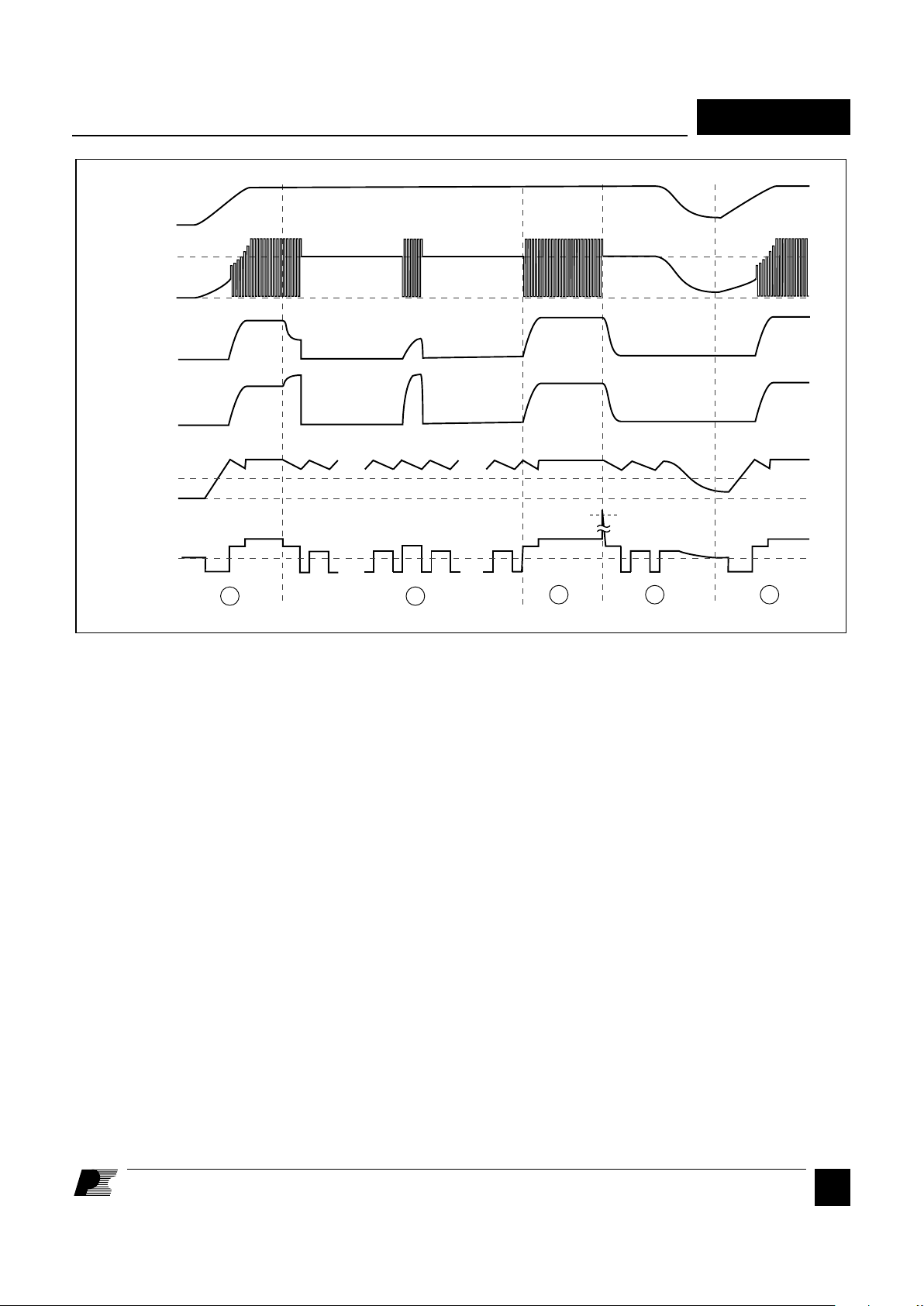
PI-1119-110194
V
IN
V
OUT
0
I
OUT
0
1 2
143
DRAIN
0
V
IN
V
C
0
••• •••
12 12 81
0
I
C
••• •••
12
8
812 81
V
C(reset)
45 mA
Shutdown/Auto-restart
To minimize TOPSwitch power
dissipation, the shutdown/auto-restart
circuit turns the power supply on and off
at a duty cycle of typically 5% if an out
of regulation condition persists. Loss of
regulation interrupts the external current
into the CONTROL pin. VC regulation
changes from shunt mode to the
hysteretic auto-restart mode described
above. When the fault condition is
removed, the power supply output
becomes regulated, VC regulation returns
to shunt mode, and normal operation of
the power supply resumes.
Latching Shutdown
The output overvoltage protection latch
is activated by a high-current pulse into
the CONTROL pin. When set, the latch
turns off the TOPSwitch output.
Activating the power-up reset circuit by
removing and restoring input power, or
momentarily pulling the CONTROL pin
below the power-up reset threshold resets
the latch and allows TOPSwitch to
resume normal power supply operation.
VC is regulated in hysteretic mode when
the power supply is latched off.
Overtemperature Protection
Temperature protection is provided by a
precision analog circuit that turns the
output MOSFET off when the junction
temperature exceeds the thermal
shutdown temperature (typically 145°C).
Activating the power-up reset circuit by
removing and restoring input power or
momentarily pulling the CONTROL pin
below the power-up reset threshold resets
the latch and allows TOPSwitch to
resume normal power supply operation.
VC is regulated in hysteretic mode when
the power supply is latched off.
High-voltage Bias Current Source
This current source biases TOPSwitch
from the DRAIN pin and charges the
CONTROL pin external capacitance
(CT) during start-up or hysteretic
operation. Hysteretic operation occurs
during auto-restart and latched
shutdown. The current source is switched
on and off with an effective duty cycle of
approximately 35%. This duty cycle is
determined by the ratio of CONTROL
pin charge (IC) and discharge currents
(I
CD1
and I
CD2
). This current source is
turned off during normal operation when
the output MOSFET is switching.
Figure 6. Typical Waveforms for (1) Normal Operation, (2) Auto-restart, (3) Latching Shutdown, and (4) Power Down Reset.
E
7/96
6
TOP100-4
current will flow into the control pin.
Increasing control pin current decreases
the duty cycle until a stable operating
point is reached. The output voltage is
proportional to the bias voltage by the
turns ratio of the output to bias windings.
C5 is used to bypass the CONTROL pin.
C5 also provides loop compensation for
the power supply by shunting AC
currents around the CONTROL pin
dynamic impedance, and also determines
the auto-restart frequency during startup and auto-restart conditions. See DN8 for more information regarding bias
supplies.
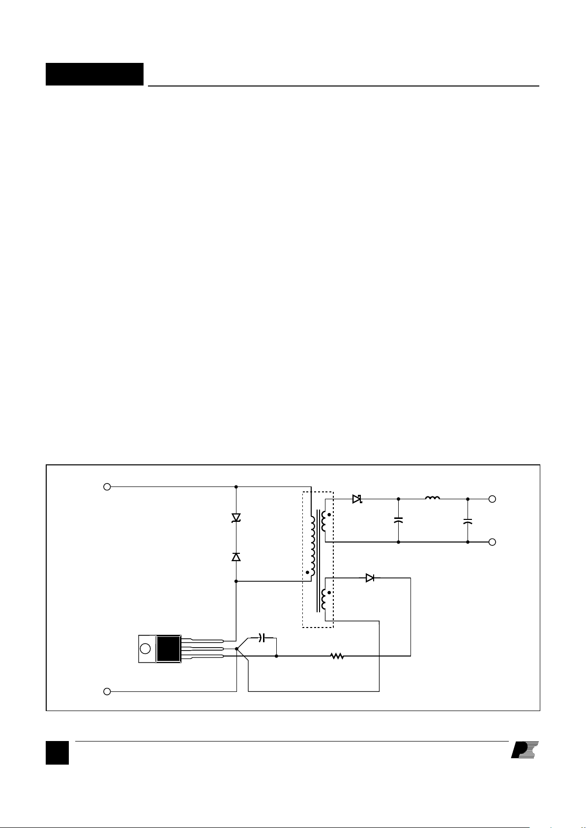
General Circuit Operation
Primary Feedback Regulation
The circuit shown in Figure 7 is a simple
5 V, 5 W bias supply using the TOP100.
This flyback power supply employs
primary-side regulation from a
transformer bias winding. This approach
is best for low-cost applications requiring
isolation and operation within a narrow
range of load variation. Line and load
regulation of ±5% or better can be
achieved from 10% to 100% of rated
load.
Voltage feedback is obtained from the
transformer (T1) bias winding, which
eliminates the need for optocoupler and
secondary-referenced error amplifier.
High-voltage DC is applied to the
primary winding of T1. The other side
of the transformer primary is driven by
Figure 7. Schematic Diagram of a Minimum Parts Count 5 V, 5 W Bias Supply Utilizing the TOP100.
the integrated high-voltage MOSFET
transistor within the TOP100 (U1). The
circuit operates at a switching frequency
of 100 kHz, set by the internal oscillator
of the TOP100. The clamp circuit
implemented by VR1 and D1 limits the
leading-edge voltage spike caused by
transformer leakage inductance to a safe
value. The 5 V power secondary winding
is rectified and filtered by D2, C2, C3,
and L1 to create the 5 V output voltage.
The output of the T1 bias winding is
rectified and filtered by D3, R1, and C5.
The voltage across C5 is regulated by
U1, and is determined by the 5.7 V
internal shunt regulator at the
CONTROL pin of U1. When the
rectified bias voltage on C5 begins to
exceed the shunt regulator voltage,
PI-1767-020296
5 V
RTN
C5
47 µF
U1
TOP100YAI
D2
1N5822
D3
1N4148
L1
(Bead)
C2
330 µF
25 V
C3
150 µF
25 V
T1
D1
UF4004
DC
INPUT
VR1
P6KE91
R1
22 Ω
CIRCUIT PERFORMANCE:
Load Regulation - ±4%
(10% to 100%)
Line Regulation - ±1.5%
95 to 185 V DC
Ripple Voltage ±25 mV
DRAIN
SOURCE
CONTROL
 Loading...