

Power Integrations TNY380PNG, TinySwitch-PK Datasheet
TNY375-380
TinySwitch-PK Family
www.powerint.com May 2007
Energy-Efcient, Off-Line Switcher With
Enhanced Peak Power Performance
®
Output Power Table
Product
3
230 VAC ± 15% 85-265 VAC
Adapter
1
Open
Frame
2
Peak Adapter
1
Open
Frame
2
Peak
TNY375 P 8.5 W 15 W 16.5 W 6 W 11.5 W 12.5 W
TNY376 P 10 W 19 W 22 W 7 W 15 W 17 W
TNY377 P 13 W 23.5 W
28 W
8 W 18 W 23 W
TNY378 P 16 W 28 W 34 W 10 W 21.5 W 27 W
TNY379 P 18 W 32 W 39 W 12 W 25 W 31 W
TNY380 P 20 W 36.5 W 45 W 14 W 28.5 W 35 W
Table 1. Output Power Table.
Notes:
1. Minimum continuous power in a typical non-ventilated enclosed adapter
measured at +50 °C ambient. Use of an external heatsink will increase power
capability.
2. Minimum continuous power in an open frame design (see Key Applications
Considerations).
3. Packages: P: DIP-8C. Available as lead free (with N suffix). See Part Ordering
Information.
Product Highlights
Lowest System Cost with Enhanced Flexibility
Simple ON/OFF control, no loop compensation needed
Unique Peak Mode feature extends power range without
increasing transformer size
Maximum frequency and current limit boosted at peak loads
Selectable current limit through BP/M capacitor value
Higher current limit further extends maximum power in open
frame applications
Lower current limit improves efficiency in enclosed adapter
applications
Allows optimum TinySwitch-PK choice by swapping devices
with no other circuit redesign
Tight I2f parameter tolerance reduces system cost:
Maximizes MOSFET and magnetics power delivery
ON time extension – typically extends low line regulation range/
hold-up time to reduce input bulk capacitance
Self-biased: no bias winding required for TNY375-376; winding
required for TNY377-380
Frequency jittering reduces EMI filter costs
Optimized pin out eases pcb/external heatsinking
Quiet source-connected heatsink pins for low EMI
Enhanced Safety and Reliability Features
Accurate hysteretic thermal shutdown with automatic recovery
provides complete system level overload protection and
eliminates need for manual reset
Auto-restart delivers <3% maximum power in short circuit and
open loop fault conditions
Output overvoltage shutdown with optional Zener
Line undervoltage detect threshold set using a single optional
resistor
Very low component count enhances reliability and enables
single sided printed circuit board layout
High bandwidth provides fast turn on with no overshoot and
excellent transient load response
Extended creepage between DRAIN and all other pins improves
field reliability
EcoSmart®– Extremely Energy Efficient
Easily meets all global energy efficiency regulations
No-load <170 mW at 265 VAC without bias winding, <60 mW
with bias winding
ON/OFF control provides constant efficiency down to very light
loads – ideal for mandatory CEC efficiency regulations and 1 W
PC standby requirements
Applications
Applications with high peak-to-continuous power demands –
DVDs, set-top decoders, active speakers (e.g. PC audio),
audio amplifiers, modems, photo printers
•
•
•
•
•
•
•
•
•
•
•
•
•
•
•
•
•
•
•
•
•
•
•
•
•
Description
TinySwitch-PK incorporates a 700 V MOSFET, oscillator, highvoltage switched current source, current limit (user selectable),
and thermal shutdown circuitry. A unique peak mode feature
boosts current limit and frequency for peak load conditions. The
boosted current limit provides the peak output power while the
increased peak mode frequency ensures the transformer can be
sized for continuous load conditions rather than peak power
demands.
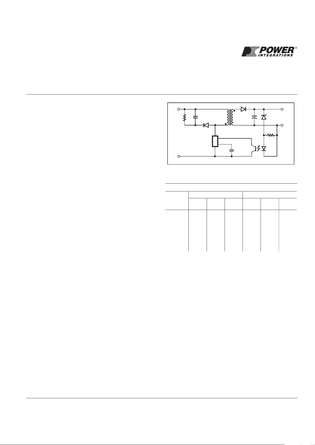
PI-4266-010906
Wide-Range
HV DC Input
D
S
EN/UV
BP/M
+
-
+
-
DC
Output
TinySwitch-PK
Figure 1. Typical Standby Application.
Rev. A 05/07
2
TNY375-380
www.powerint.com
Pin Functional Description
DRAIN (D) Pin:
This pin is the power MOSFET drain connection. It provides
internal operating current for both start-up and steady-state
operation.
BYPASS/MULTI-FUNCTION (BP/M) Pin:
This pin has multiple functions:
It is the connection point for an external bypass capacitor for
the internally generated 5.85 V supply.
It is a mode selector for the current limit value, depending on
the value of the capacitance added. Use of a 0.1 mF
capacitor results in the standard current limit value. Use of a
1 mF capacitor results in the current limit being reduced to
that of the next smaller device size (TNY376-380). Use of a
10 mF capacitor results in the current limit being increased to
that of the next larger device (TNY377-379).
It provides a shutdown function. When the current into the
bypass pin exceeds 7 mA, the device latches off until the
BP/M voltage drops below 4.9 V, during a power down or
when a line undervoltage is detected. This can be used to
provide an output overvoltage function with a Zener diode
connected from the BP/M pin to a bias winding supply.
1.
2.
3.
ENABLE/UNDERVOLTAGE (EN/UV) Pin:
This pin has dual functions: enable input and line undervoltage
sense. During normal operation, switching of the power
MOSFET is controlled by this pin. MOSFET switching is
terminated when a current greater than a threshold current is
drawn from this pin. Switching resumes when the current being
PI-4550-121406
CLOCK
OSCILLATOR
5.85 V
4.9 V
SOURCE
(S)
SRQ
DC
MAX
BYPASS/
MULTI-FUNCTION
(BP/M)
+
-
V
I
LIMIT
FAULT
PRESENT
CURRENT LIMIT
COMPARATOR
ENABLE
LEADING
EDGE
BLANKING
THERMAL
SHUTDOWN
+
-
DRAIN
(D)
REGULATOR
5.85 V
BYPASS PIN
UNDER-VOLTAGE
1.0 V + V
T
ENABLE/
UNDER-
VOLTAGE
(EN/UV)
Q
115 mA 25 mA
LINE UNDER-VOLTAGE
RESET
AUTORESTART
COUNTER
JITTER 2X
1.0 V
6.4 V
BYPASS
CAPACITOR
SELECT AND
CURRENT
LIMIT STATE
MACHINE
OVP
LATCH
RESET
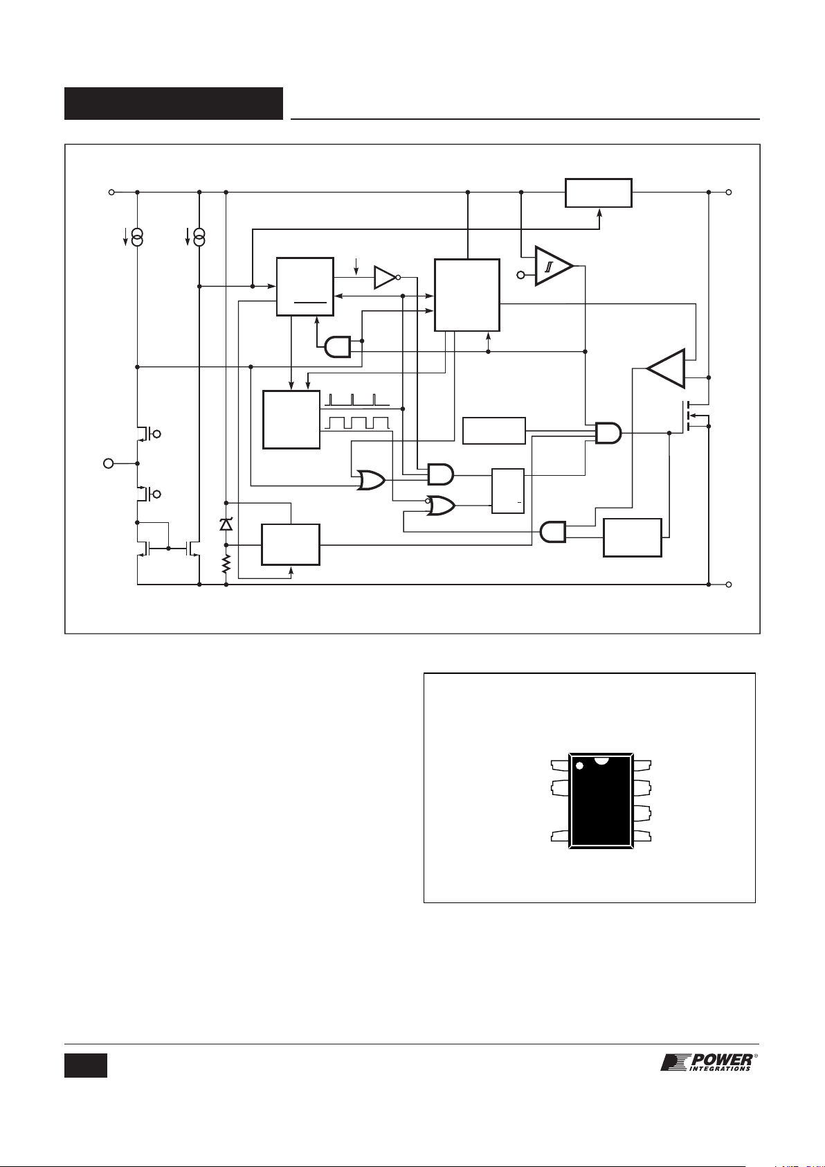
Figure 2 Functional Block Diagram.
PI-4348-032806
D
S
BP/M
S
S
EN/UV
P Package (DIP-8C)
8
5
7
1
4
2
S
6
Figure 3. Pin Configuration.
Rev. A 05/07
3
TNY375-380
www.powerint.com
pulled from the pin drops to less than a threshold current. A
modulation of the threshold current reduces group pulsing.
The threshold current is between 75 mA and 115 mA.
The EN/UV pin also senses line undervoltage conditions
through an external resistor connected to the DC line voltage.
If there is no external resistor connected to this pin,
TinySwitch-PK detects its absence and disables the line undervoltage function.
SOURCE (S) Pin:
This pin is internally connected to the output MOSFET source
for high voltage power return and control circuit common.
TinySwitch-PK Functional Description
TinySwitch-PK combines a high voltage power MOSFET switch
with a power supply controller in one device. Unlike
conventional PWM (pulse width modulator) controllers, it uses a
simple ON/OFF control to regulate the output voltage.
The controller consists of an oscillator, enable circuit (sense and
logic), current limit state machine, 5.85 V regulator, BYPASS/
MULTI-FUNCTION pin undervoltage, overvoltage circuit, and
current limit selection circuitry, over-temperature protection,
current limit circuit, leading edge blanking, and a 700 V power
MOSFET. TinySwitch-PK incorporates additional circuitry for
line undervoltage sense, auto-restart, adaptive switching cycle
on-time extension, and frequency jitter. Figure 2 shows the
functional block diagram with the most important features.
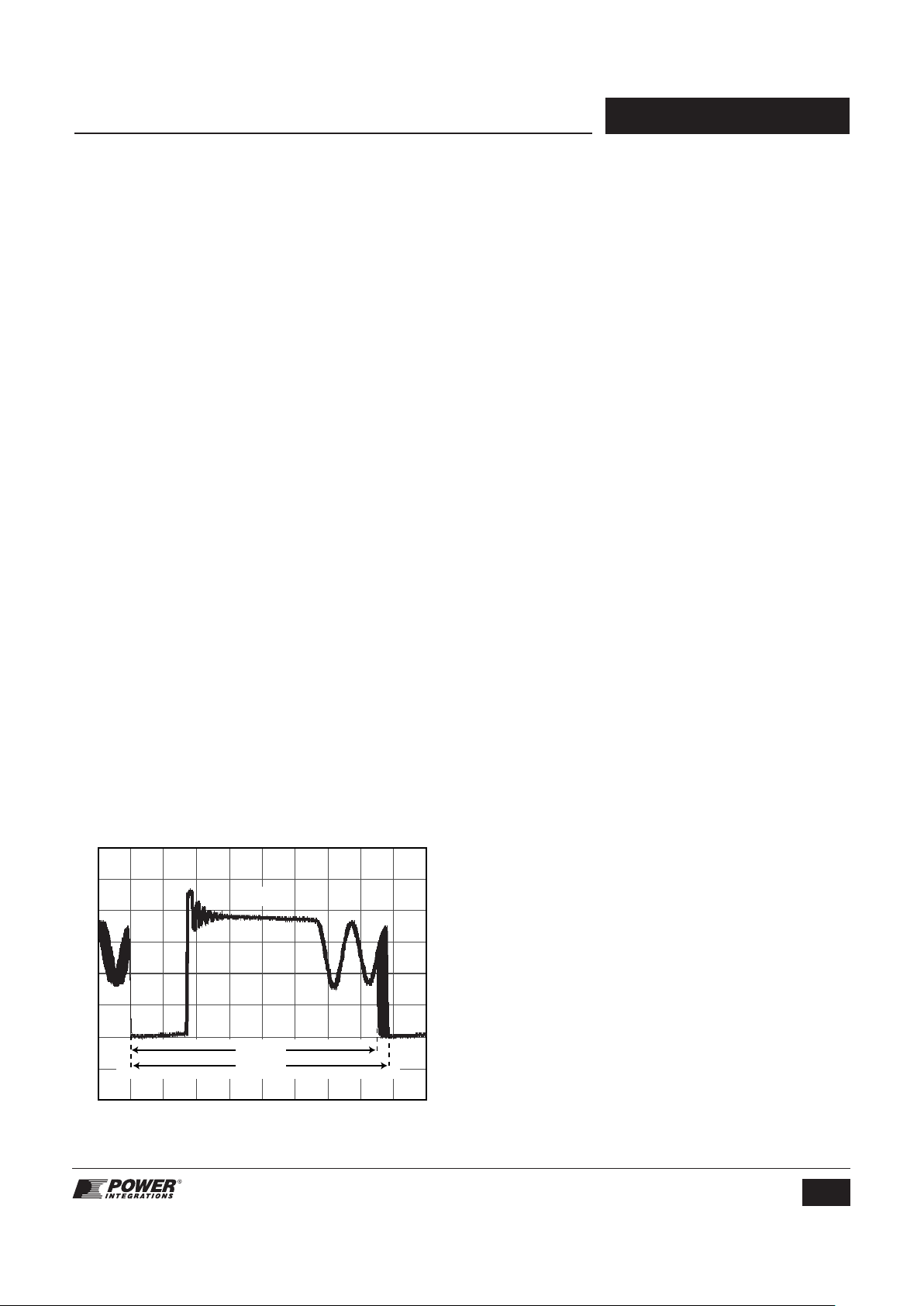
Oscillator
The typical oscillator frequency is internally set to an average of
264 kHz (at the highest current limit level). Two signals are
generated from the oscillator: the maximum duty cycle signal
(DC
MAX
) and the clock signal that indicates the beginning of
each cycle.
The oscillator incorporates circuitry that introduces a small
amount of frequency jitter, typically ±3% of the oscillator
frequency, to minimize EMI emission. The modulation rate of
the frequency jitter is set to 1 kHz to optimize EMI reduction for
both average and quasi-peak emissions. The frequency jitter
should be measured with the oscilloscope triggered at the
falling edge of the DRAIN waveform. The waveform in Figure 4
illustrates the frequency jitter with an oscillator frequency of
264 kHz.
Enable Input and Current Limit State Machine
The enable input circuit at the EN/UV pin consists of a low
impedance source follower output set at 1.2 V. The current
through the source follower is limited to 115 mA. When the
current out of this pin exceeds the threshold current, a low logic
level (disable) is generated at the output of the enable circuit
until the current out of this pin is reduced to less than the
threshold current. This enable circuit output is sampled at the
beginning of each cycle on the rising edge of the clock signal. If
high, the power MOSFET is turned on for that cycle (enabled). If
low, the power MOSFET remains off (disabled). Since the
sampling is done only at the beginning of each cycle,
subsequent changes in the EN/UV pin voltage or current during
the remainder of the cycle are ignored. When a cycle is
disabled, the EN/UV pin is sampled at 264 kHz. This faster
sampling enables the power supply to respond faster without
being required to wait for completion of the full period.
The current limit state machine reduces the current limit by
discrete amounts at light loads when TinySwitch-PK is likely to
switch in the audible frequency range. The lower current limit
raises the effective switching frequency above the audio range
and reduces the transformer flux density, including the
associated audible noise. The state machine monitors the
sequence of enable events to determine the load condition and
adjusts the current limit level accordingly in discrete amounts.
Under most operating conditions (except when close to noload), the low impedance of the source follower keeps the
voltage on the EN/UV pin from going much below 1.2 V in the
disabled state. This improves the response time of the
optocoupler that is usually connected to this pin.
5.85 V Regulator and 6.4 V Shunt Voltage Clamp
The 5.85 V regulator charges the bypass capacitor connected
to the BYPASS pin to 5.85 V by drawing a current from the
voltage on the DRAIN pin whenever the MOSFET is off. The
BYPASS/MULTI-FUNCTION pin is the internal supply voltage
node. When the MOSFET is on, the device operates from the
energy stored in the bypass capacitor. Extremely low power
consumption of the internal circuitry allows the TNY375 and
TNY376 to operate continuously from current taken from the
DRAIN pin. A bypass capacitor value of 0.1 mF is sufficient for
both high frequency decoupling and energy storage.
In addition, there is a 6.4 V shunt regulator clamping the
BYPASS/MULTI-FUNCTION pin at 6.4 V when current is
provided to the BYPASS/MULTI-FUNCTION pin through an
external resistor. This facilitates powering of TinySwitch-PK
externally through a bias winding as required for TNY377-380.
Powering the TinySwitch-PK externally in this way also
decreases the no-load consumption to well below 50 mW.
600
0 2.5 5
272 kHz
256 kHz
V
DRAIN
Time (µs)
PI-4539-120406
500
400
300
200
100
0
Figure 4. Frequency Jitter.
Rev. A 05/07
4
TNY375-380
www.powerint.com
BYPASS/MULTI-FUNCTION Pin Undervoltage
The BYPASS/MULTI-FUNCTION pin undervoltage circuitry
disables the power MOSFET when the BYPASS/MULTIFUNCTION pin voltage drops below 4.9 V in steady state
operation. Once the BYPASS/MULTI-FUNCTION pin voltage
drops below 4.9 V in steady state operation, it must rise back to
5.85 V to enable (turn-on) the power MOSFET.
Over Temperature Protection
The thermal shutdown circuitry senses the die temperature.
The threshold is typically set at 142 °C with 75 °C hysteresis.
When the die temperature rises above this threshold, the power
MOSFET is disabled and remains disabled, until the die
temperature falls by 75 °C, at which point it is re-enabled. A
large hysteresis of 75 °C (typical) is provided to prevent
overheating of the PC board due to a continuous fault condition.
Current Limit
The current limit circuit senses the current in the power
MOSFET. When this current exceeds the internal threshold
(I
LIMIT
), the power MOSFET is turned off for the remainder of that
cycle. The current limit state machine reduces the current limit
threshold by discrete amounts under medium and light loads.
The leading edge blanking circuit inhibits the current limit
comparator for a short time (t
LEB
) after the power MOSFET is
turned on. This leading edge blanking time has been set so
that current spikes caused by typical capacitance and
secondary-side rectifier reverse recovery time will not cause
premature termination of the switching pulse.
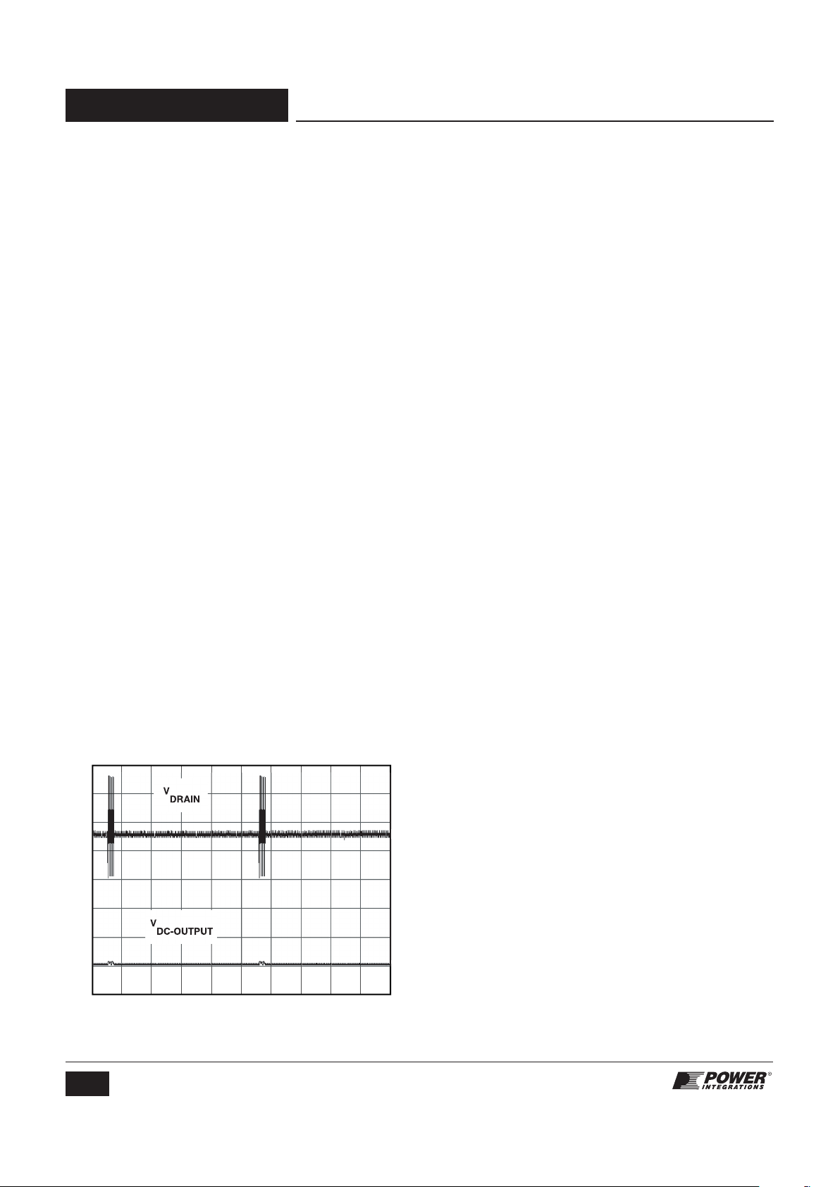
Auto-Restart
In the event of a fault condition such as output overload, output
short circuit, or an open loop condition, TinySwitch-PK enters
into auto-restart operation. An internal counter clocked by the
oscillator is reset every time the EN/UV pin is pulled low. If the
EN/UV pin is not pulled low for 8192 switching cycles
(or 32 ms), the power MOSFET switching is normally disabled
for 1 second (except in the case of line undervoltage condition,
in which case it is disabled until the condition is removed). The
auto-restart alternately enables and disables the switching of
the power MOSFET until the fault condition is removed.
Figure 5 illustrates auto-restart circuit operation in the presence
of an output short circuit.
In the event of a line undervoltage condition, the switching of
the power MOSFET is disabled beyond its normal 1 second
until the line undervoltage condition ends.
Adaptive Switching Cycle On-Time Extension
Adaptive switching cycle on-time extension keeps the cycle on
until current limit is reached, instead of prematurely terminating
after the DC
MAX
signal goes low. This feature reduces the
minimum input voltage required to maintain regulation, typically
extending hold-up time and minimizing the size of bulk
capacitor required. The on-time extension is disabled during
the startup of the power supply, and after auto-restart, until the
power supply output reaches regulation.
Line Undervoltage Sense Circuit
The DC line voltage can be monitored by connecting an
external resistor from the DC line to the EN/UV pin. During
power-up or when the switching of the power MOSFET is
disabled in auto-restart, the current into the EN/UV pin must
exceed 25 mA to initiate switching of the power MOSFET.
During power-up, this is accomplished by holding the BYPASS/
MULTI-FUNCTION pin to 4.9 V while the line undervoltage
condition exists. The BYPASS/MULTI-FUNCTION pin then rises
from 4.9 V to 5.85 V when the line undervoltage condition goes
away. Once MOSFET switching is enabled, the DC line voltage
is ignored unless the power supply enters auto-restart mode in
the event of a fault condition. When the switching of the power
MOSFET is disabled in auto-restart mode and a line undervoltage condition exists, the auto-restart counter is stopped.
This stretches the disable time beyond its normal 1 second until
the line undervoltage condition ends.
The line undervoltage circuit also detects when there is no
external resistor connected to the EN/UV pin (less than ~1 mA
into the pin). In this case the line undervoltage function is
disabled.
TinySwitch-PK Operation
TinySwitch-PK devices operate in the current limit mode.
When enabled, the oscillator turns the power MOSFET on at the
beginning of each cycle. The MOSFET is turned off when the
current ramps up to the current limit or when the DC
MAX
limit is
reached (applicable when On-Time Extension is disabled).
Since the highest current limit level and frequency of a
TinySwitch-PK design are constant, the power delivered to the
load is proportional to the primary inductance of the transformer
and peak primary current squared. Hence, designing the
supply involves calculating the primary inductance of the
transformer for the maximum output power required. If the
TinySwitch-PK is appropriately chosen for the power level, the
current in the calculated inductance will ramp up to current limit
before the DC
MAX
limit is reached.
PI-4320-030106
0
1000 2000
Time (ms)
0
5
0
10
100
200
300
V
DRAIN
V
DC-OUTPUT
Figure 5. Auto-Restart Operation.
Rev. A 05/07
5
TNY375-380
www.powerint.com
Enable Function
TinySwitch-PK senses the EN/UV pin to determine whether or
not to proceed with the next switching cycle. The sequence of
cycles is used to determine the current limit. Once a cycle is
started, it always completes the cycle (even when the EN/UV
pin changes state halfway through the cycle). This operation
results in a power supply in which the output voltage ripple is
determined by the output capacitor, amount of energy per
switch cycle, and the delay of the feedback.
The EN/UV pin signal is generated on the secondary by
comparing the power supply output voltage with a reference
voltage. The EN/UV pin signal is high when the power supply
output voltage is less than the reference voltage.
In a typical implementation, the EN/UV pin is driven by an
optocoupler. The collector of the optocoupler transistor is
connected to the EN/UV pin, and the emitter is connected to
the SOURCE pin. The optocoupler LED is connected in series
with a Zener diode across the DC output voltage to be
regulated. When the output voltage exceeds the target
regulation voltage level (optocoupler LED voltage drop plus
Zener voltage), the optocoupler LED will start to conduct,
pulling the EN/UV pin low. The Zener diode can be replaced by
a TL431 reference circuit for improved accuracy.
ON/OFF Operation with Current Limit State Machine
The internal clock of the TinySwitch-PK runs at all times. At the
beginning of each clock cycle, it samples the EN/UV pin to
decide whether or not to implement a switch cycle, and based
on the sequence of samples over multiple cycles, it determines
the appropriate current limit. At high loads, the state machine
sets the current limit to its highest value. With TinySwitch-PK,
when the state machine sets the current limit to its highest
value, the oscillator frequency is also doubled, providing the
unique peak mode operation. At lighter loads, the state
machine sets the current limit to reduced values. At these lower
current limit levels, the oscillator frequency returns to the
standard value.
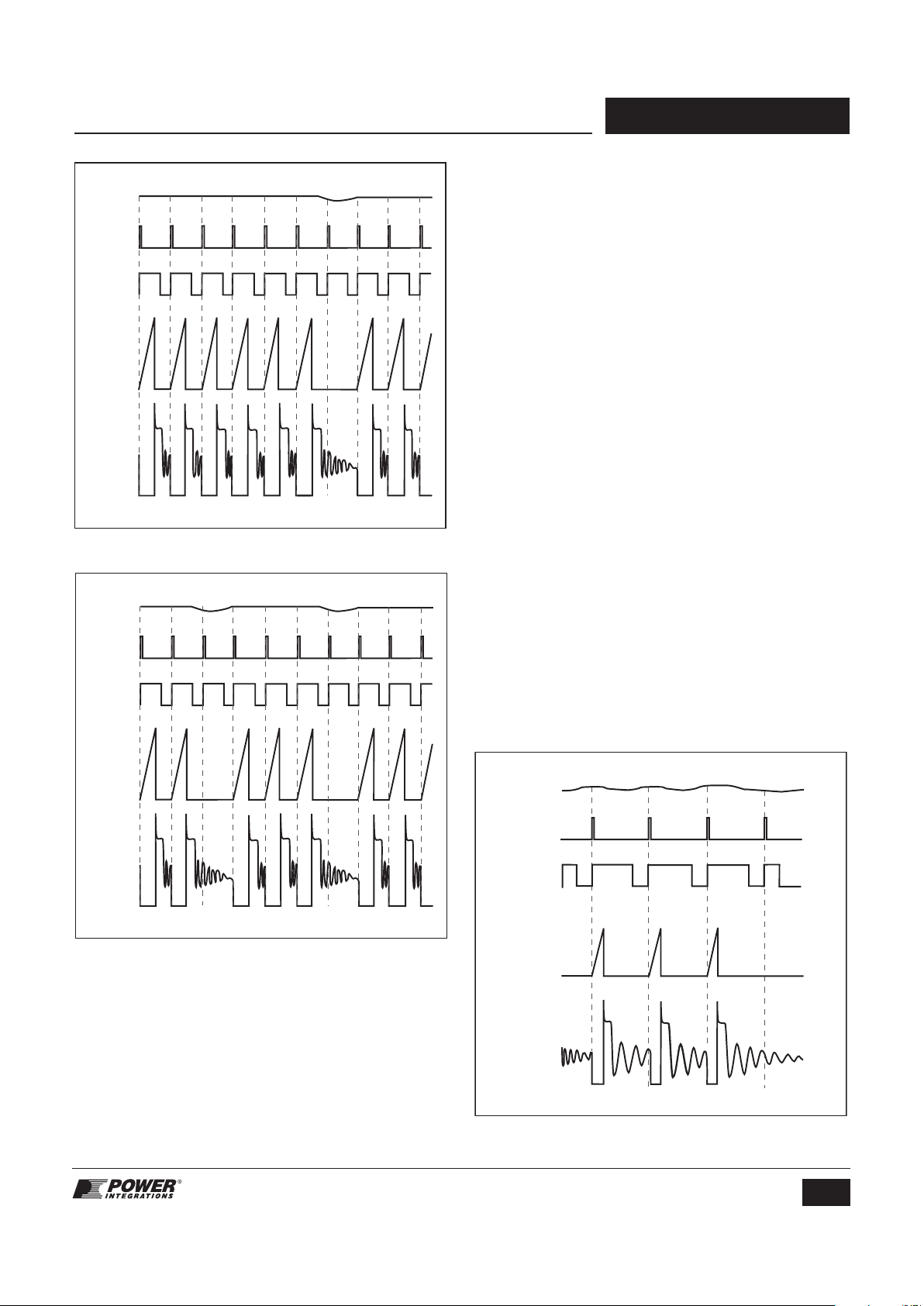
At near maximum load, TinySwitch-PK will conduct during
nearly all of its clock cycles (Figure 6). At slightly lower load, it
will “skip” additional cycles in order to maintain voltage
regulation at the power supply output (Figure 7). At medium
loads, more cycles will be skipped, the current limit will be
V
DRAIN
V
EN
CLOCK
DC
DRAIN
I
MAX
PI-2749-082305
V
DRAIN
V
EN
CLOCK
DC
DRAIN
I
MAX
PI-2667-082305
Figure 6. Operation at Near Maximum Loading (f
OSC
264 kHz).
Figure 7. Operation at Moderately Heavy Loading (f
OSC
264 kHz).
PI-4540-050407
V
DRAIN
V
EN
CLOCK
DC
DRAIN
I
MAX
Figure 8. Operation at Medium Loading (f
OSC
132 kHz).
Rev. A 05/07
6
TNY375-380
www.powerint.com
PI-4541-042507
V
DRAIN
V
EN
CLOCK
D
DRAIN
I
MAX
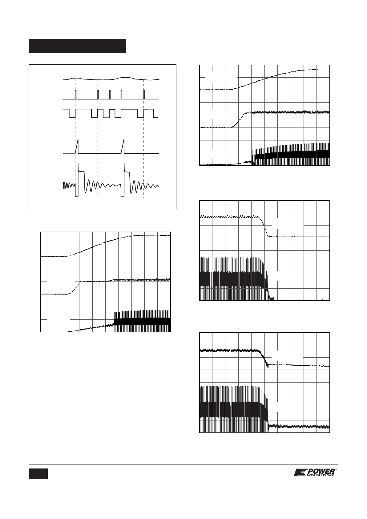
Figure 9. Operation at Very Light Load (f
OSC
132 kHz).
0
1 2
Time (ms)
0
200
400
5
0
10
0
100
200
PI-2383-030801
V
DC-INPUT
V
BYPASS
V
DRAIN
PI-2381-1030801
0
1 2
Time (ms)
0
200
400
5
0
10
0
100
200
V
DC-INPUT
V
BYPASS
V
DRAIN
PI-2348-030801
0
.5 1
Time (s)
0
100
200
300
0
100
200
400
V
DC-INPUT
V
DRAIN
PI-2395-030801
0
2.5 5
Time (s)
0
100
200
400
300
0
100
200
V
DC-INPUT
V
DRAIN
Figure 10. Power-up With Optional External UV Resistor (4 MW) Connected
to EN/UV Pin.
Figure 11. Power-up Without Optional External UV Resistor Connected
to EN/UV Pin.
Figure 12. Normal Power-down Timing (Without UV Resistor).
Figure 13. Slow Power-down Timing With Optional External (4 MW) UV Resistor
Connected to EN/UV Pin.
 Loading...