

Page 1
LNK362-364
LinkSwitch-XT Family
Energy Efficient, Low Power Off-Line Switcher IC
Product Highlights
Optimized for Lowest System Cost
• Proprietary IC trimming and transformer construction
techniques enable Clampless™ designs with LNK362
for lower system cost, component count and higher
efficiency
• Fully integrated auto-restart for short-circuit and
open loop protection
• Self-biased supply – saves transformer auxiliary
winding and associated bias supply components
• Frequency jittering greatly reduces EMI
• Meets HV creepage requirements between DRAIN and
all other pins both on the PCB and at the package
• Lowest component count switcher solution
Features Superior to Linear/RCC
• Accurate hysteretic thermal shutdown protection –
automatic recovery improves field reliability
• Universal input range allows worldwide operation
• Simple ON/OFF control, no loop compensation
needed
• Eliminates bias winding – simpler, lower cost
transformer
• Very low component count – higher reliability and
single side printed circuit board
• Auto-restart reduces delivered power by 95% during
short-circuit and open loop fault conditions
• High bandwidth provides fast turn-on with no
overshoot and excellent transient load response
EcoSmart™– Extremely Energy-Efficient
• Easily meets all global energy efficiency regulations
with no added components
• No-load consumption <300 mW without bias winding
at 265 VAC input (<50 mW with bias winding)
• ON/OFF control provides constant efficiency to very
light loads – ideal for mandatory CEC regulations
Applications
• Chargers/adapters for cell/cordless phones, PDAs,
digital cameras, MP3/portable audio players, and
shavers
• Supplies for appliances, industrial systems, and
metering
Description
LinkSwitch™-XT incorporates a 700 V power MOSFET,
oscillator, simple ON/OFF control scheme, a high-voltage
switched current source, frequency jittering, cycle-by-
(1)
+
+
Open
Frame
(2)
+
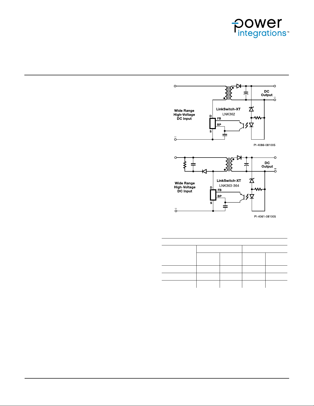
a) Clampless flyback converter with LNK362
+
b) Flyback converter with LNK363/4
Figure 1. Typical Application with LinkSwitch-XT.
Output Power Table
Product
LNK362P/G/D 2.8 W 2.8 W 2.6 W 2.6 W
LNK363P/G/D 5 W 7.5 W 3.7 W 4.7 W
LNK364P/G/D
Table 1. Output Power Table.
Notes:
1. Minimum continuous power in a typical non-ventilated enclosed
adapter measured at 50 °C ambient.
2. Minimum practical continuous power in an open frame design with
adequate heat sinking, measured at 50 °C ambient.
3. Packages: P: DIP-8B, G: SMD-8B, D: SO-8C. Please see Part
Ordering Information.
4. See Key Application Considerations section for complete description
of assumptions.
3)
(4)
230 VAC ±15% 85-265 VAC
Open
Adapter
(1)
Frame
5.5 W 9 W 4 W 6 W
(2)
Adapter
cycle current limit and thermal shutdown circuitry onto
a monolithic IC. The start-up and operating power are
derived directly from the DRAIN pin, eliminating the need
for a bias winding and associated circuitry.
www.power.com October 2020
This Product is Covered by Patents and/or Pending Patent Applications.
Page 2
LNK362-364
PI-7192-110413
FB
D
S
BP
S
S
S
P Package (DIP-8B)
G Package (SMD-8B)
D Package (SO-8C)
8
5
7
1
4
2
3
BP
FB
D
1
2
4
8
7
6
5
S
S
S
S
BYPASS
(BP)
FEEDBACK
(FB)
VFB -V
DRAIN
REGULATOR
5.8 V
FAULT
PRESENT
AUTO-
RESTART
COUNTER
CLOCK
RESET
6.3 V
JITTER
CLOCK
DC
MAX
OSCILLATOR
TH
5.8 V
4.8 V
SHUTDOWN
+
-
THERMAL
SRQ
BYPASS PIN
UNDER-VOLTAGE
Q
CURRENT LIMIT
COMPARATOR
+
-
LEADING
EDGE
BLANKING
V
I
LIMIT
(D)
SOURCE
(S)
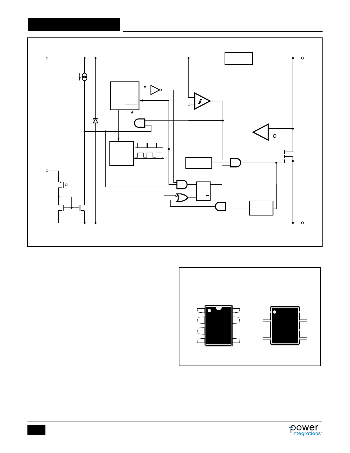
Figure 2. Functional Block Diagram.
Pin Functional Description
DRAIN (D) Pin:
Power MOSFET drain connection. Provides internal
operating current for both start-up and steady-state
operation.
BYPASS (BP) Pin:
Connection point for a 0.1 µF external bypass capacitor
for the internally generated 5.8 V supply. If an external
bias winding is used, the current into the BP pin must not
exceed 1 mA.
FEEDBACK (FB) Pin:
During normal operation, switching of the power MOSFET
is controlled by this pin. MOSFET switching is disabled
when a current greater than 49 µA is delivered into this
pin.
SOURCE (S) Pin:
This pin is the power MOSFET source connection.
It is also the ground reference for the BYPASS and
FEEDBACK pins.
2
Rev. H 10/20
PI-4232-110205
Figure 3. Pin Conguration.
www.power.com
Page 3
LNK362-364
PI-4047-110205
100
200
400
500
600
300
LinkSwitch-XT Functional Description
LinkSwitch-XT combines a high-voltage power MOSFET
switch with a power supply controller in one device. Unlike
conventional PWM (pulse width modulator) controllers,
a simple ON/OFF control regulates the output voltage. The
controller consists of an oscillator, feedback (sense and
logic) circuit, 5.8 V regulator, BYPASS pin undervoltage
circuit, over-temperature protection, frequency jittering,
current limit circuit, and leading edge blanking integrated
with a 700 V power MOSFET. The LinkSwitch-XT
incorporates additional circuitry for auto-restart.
Oscillator
The typical oscillator frequency is internally set to an
average of 132 kHz. Two signals are generated from the
oscillator: the maximum duty cycle signal (DC
clock signal that indicates the beginning of each cycle.
The oscillator incorporates circuitry that introduces a
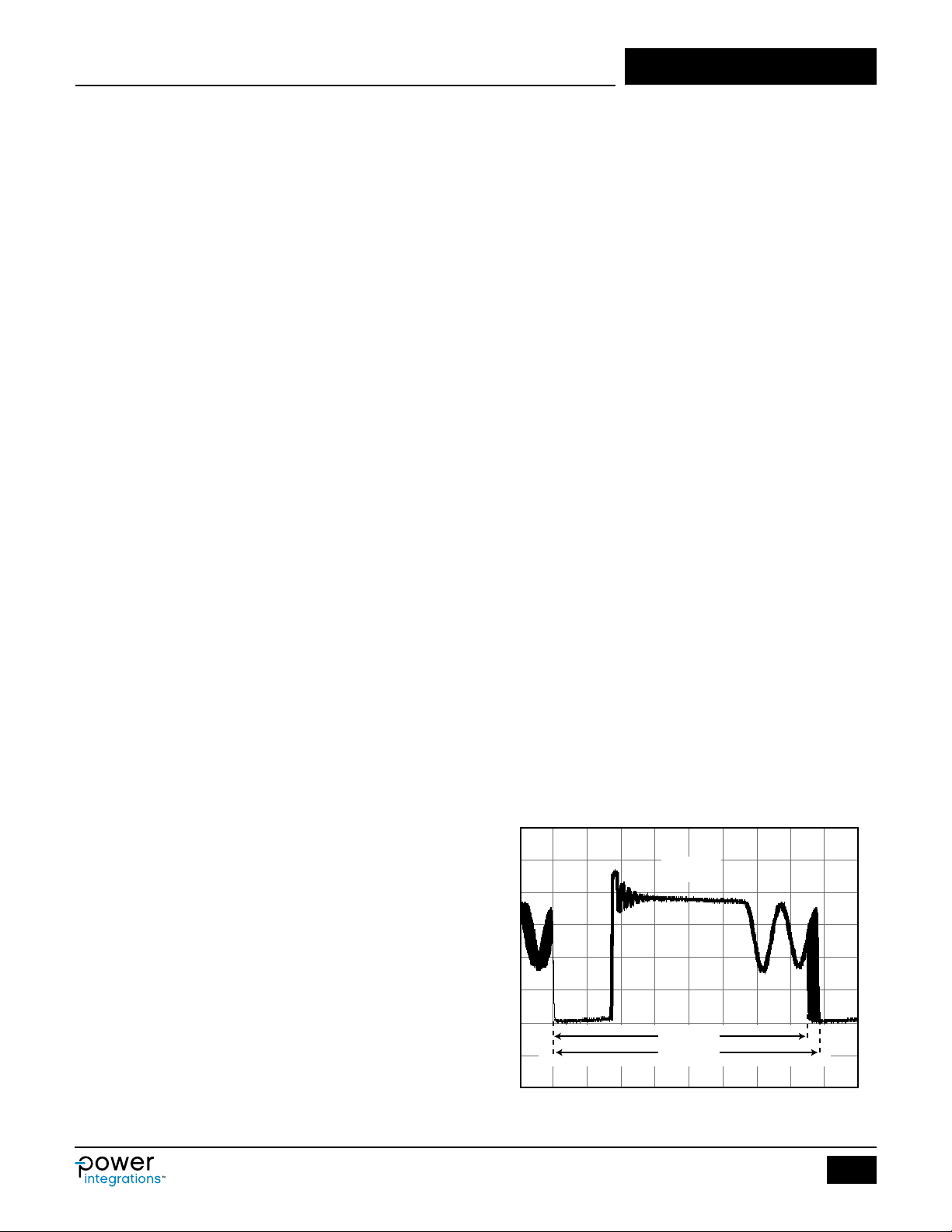
small amount of frequency jitter, typically 9 kHz peakto-peak, to minimize EMI emission. The modulation rate
of the frequency jitter is set to 1.5 kHz to optimize EMI
reduction for both average and quasi-peak emissions. The
frequency jitter should be measured with the oscilloscope
triggered at the falling edge of the DRAIN waveform. The
waveform in Figure 4 illustrates the frequency jitter.
Feedback Input Circuit
The feedback input circuit at the FB pin consists of a
low impedance source follower output set at 1.65 V for
LNK362 and 1.63 V for LNK363/364. When the current
delivered into this pin exceeds 49 µA, a low logic level
(disable) is generated at the output of the feedback circuit.
This output is sampled at the beginning of each cycle
on the rising edge of the clock signal. If high, the power
MOSFET is turned on for that cycle (enabled), otherwise
the power MOSFET remains off (disabled). Since the
sampling is done only at the beginning of each cycle,
subsequent changes in the FB pin voltage or current
during the remainder of the cycle are ignored.
) and the
MAX
BYPASS pin through an external resistor. This facilitates
powering of the device externally through a bias winding
to decrease the no-load consumption to less than 50 mW.
BYPASS Pin Undervoltage
The BYPASS pin undervoltage circuitry disables the power
MOSFET when the BYPASS pin voltage drops below 4.8 V.
Once the BYPASS pin voltage drops below 4.8 V, it must
rise back to 5.8 V to enable (turn-on) the power MOSFET.
Over-Temperature Protection
The thermal shutdown circuitry senses the die temperature.
The threshold is set at 142 °C typical with a 75 °C
hysteresis. When the die temperature rises above this
threshold (142 °C) the power MOSFET is disabled and
remains disabled until the die temperature falls by 75 °C,
at which point it is re-enabled.
Current Limit
The current limit circuit senses the current in the power
MOSFET. When this current exceeds the internal threshold
(I
), the power MOSFET is turned off for the remainder
LIMIT
of that cycle. The leading edge blanking circuit inhibits
the current limit comparator for a short time (t
) after the
LEB
power MOSFET is turned on. This leading edge blanking
time has been set so that current spikes caused by
capacitance and rectifier reverse recovery time will not
cause premature termination of the switching pulse.
Auto-Restart
In the event of a fault condition such as output overload,
output short-circuit, or an open loop condition,
LinkSwitch-XT enters into auto-restart operation. An
internal counter clocked by the oscillator gets reset
every time the FB pin is pulled high. If the FB pin is not
pulled high for approximately 40 ms, the power MOSFET
switching is disabled for 800 ms. The auto-restart
alternately enables and disables the switching of the
power MOSFET until the fault condition is removed.
5.8 V Regulator and 6.3 V Shunt Voltage Clamp
The 5.8 V regulator charges the bypass capacitor
connected to the BYPASS pin to 5.8 V by drawing a
current from the voltage on the DRAIN, whenever the
MOSFET is off. The BYPASS pin is the internal supply
voltage node. When the MOSFET is on, the LinkSwitch-XT
runs off of the energy stored in the bypass capacitor.
Extremely low power consumption of the internal circuitry
allows the device to operate continuously from the current
drawn from the DRAIN pin. A bypass capacitor value of
0.1 µF is sufficient for both high frequency decoupling and
energy storage.
In addition, there is a 6.3 V shunt regulator clamping the
BYPASS pin at 6.3 V when current is provided to the
www.power.com
V
DRAIN
0
05
Figure 4. Frequency Jitter.
136.5 kHz
127.5 kHz
Time (µs)
10
3
Rev. H 10/20
Page 4
LNK362-364
L1
1 mH
RF1
8.2 Ω
2.5 W
J1
85-265
VRMS
J2
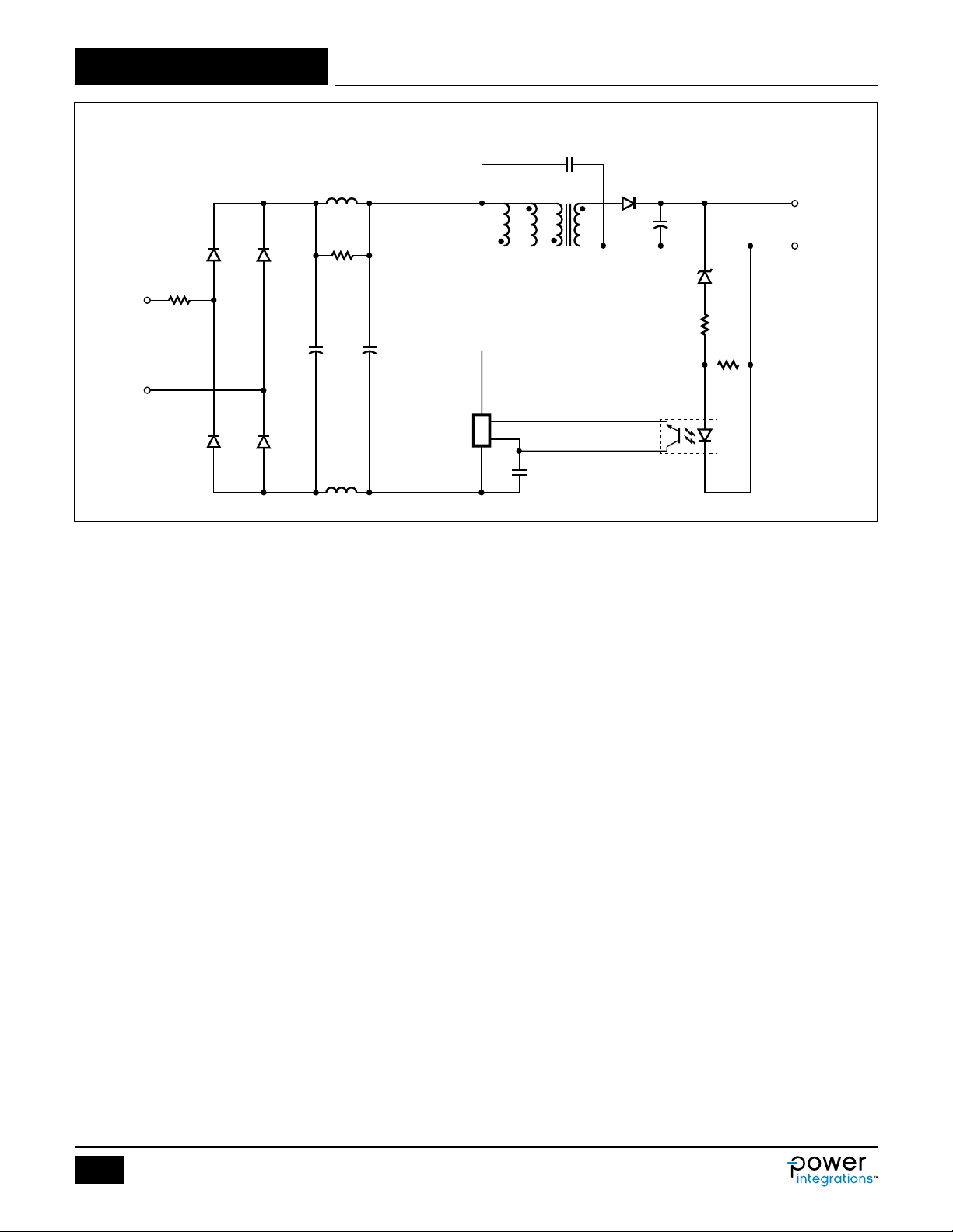
Figure 5. 2 W Universal Input CV Adapter using LNK362.
D1
1N4005D21N4005
C1
3.3 µF
400 V
D3
1N4005D41N4005
R1
3.9 k
1/8 W
L2
1 mH
C2
3.3 µF
400 V
LinkSwitch-XT
U1
LNK362P
CY1
100 pF
250 VAC
C4
D5
1N4934
330 µF
16 V
VR1
BZX79-
B5V1
5.1 V, 2%
PC817A
U2
R2
390 Ω
1/8 W
R3
1 k
1/8 W
PI-4162-110205
T1
NC NC
C3
100 nF
50 V
EE16
9
8
4
5
3
D
FB
BP
S
6.2 V,
322 mA
J3
J4
Applications Example
A 2 W CV Adapter
The schematic shown in Figure 5 is a typical implementation
of a universal input, 6.2 V ±7%, 322 mA adapter using
LNK362. This circuit makes use of the clampless
technique to eliminate the primary clamp components and
reduce the cost and complexity of the circuit.
The EcoSmart features built into the LinkSwitch-XT family
allow this design to easily meet all current and proposed
energy efficiency standards, including the mandatory
California Energy Commission (CEC) requirement for
average operating efficiency.
The AC input is rectified by D1 to D4 and filtered by the
bulk storage capacitors C1 and C2. Resistor RF1 is a
flameproof, fusible, wire wound type and functions as a
fuse, inrush current limiter and, together with the π filter
formed by C1, C2, L1 and L2, differential mode noise
attenuator. Resistor R1 damps ringing caused by L1
and L2.
This simple input stage, together with the frequency
jittering of LinkSwitch-XT, a low value Y1 capacitor and
PI’s E-Shield™ windings within T1, allow the design to
meet both conducted and radiated EMI limits with
>10 dBµV margin. The low value of CY1 is important to
meet the requirement for a very low touch current (the line
frequency current that flows through CY1) often specified
for adapters, in this case <10 µA.
The rectified and filtered input voltage is applied to the
primary winding of T1. The other side of the primary
is driven by the integrated MOSFET in U1. No primary
clamp is required as the low value and tight tolerance of
the LNK362 internal current limit allows the transformer
primary winding capacitance to provide adequate
clamping of the leakage inductance drain voltage spike.
The secondary of the flyback transformer T1 is rectified
by D5, a low cost, fast recovery diode, and filtered by
C4, a low ESR capacitor. The combined voltage drop
across VR1, R2 and the LED of U2 determines the
output voltage. When the output voltage exceeds this
level, current will flow through the LED of U2. As the LED
current increases, the current fed into the FEEDBACK pin
of U1 increases until the turnoff threshold current (~49 µA)
is reached, disabling further switching cycles of U1. At
full load, almost all switching cycles will be enabled, and
at very light loads, almost all the switching cycles will be
disabled, giving a low effective frequency and providing
high light load efficiency and low no-load consumption.
Resistor R3 provides 1 mA through VR1 to bias the Zener
closer to its test current. Resistor R2 allows the output
voltage to be adjusted to compensate for designs where
the value of the Zener may not be ideal, as they are only
available in discrete voltage ratings. For higher output
accuracy, the Zener may be replaced with a reference IC
such as the TL431.
4
Rev. H 10/20
www.power.com
Page 5

LNK362-364
The LinkSwitch-XT is completely self-powered from the
DRAIN pin, requiring only a small ceramic capacitor C3
connected to the BYPASS pin. No auxiliary winding on the
transformer is required.
Key Application Considerations
LinkSwitch-XT Design Considerations
Output Power Table
The data sheet maximum output power table (Table 1)
represents the maximum practical continuous output
power level that can be obtained under the following
assumed conditions:
1. The minimum DC input voltage is 90 V or higher for
85 VAC input, or 240 V or higher for 230 VAC input or
115 VAC with a voltage doubler. The value of the input
capacitance should be large enough to meet these
criteria for AC input designs.
2. Secondary output of 6 V with a fast PN rectifier diode.
3. Assumed efficiency of 70%.
4. Voltage only output (no secondary-side constant
current circuit).
5. Discontinuous mode operation (KP >1).
6. A primary clamp (RCD or Zener) is used.
7. The part is board mounted with SOURCE pins
soldered to a sufficient area of copper to keep the
SOURCE pin temperature at or below 100 °C.
8. Ambient temperature of 50 °C for open frame designs
and an internal enclosure temperature of 60 °C for
adapter designs.
Below a value of 1, KP is the ratio of ripple to peak
primary current. Above a value of 1, KP is the ratio of
primary MOSFET OFF time to the secondary diode
conduction time. Due to the flux density requirements
described below, typically a LinkSwitch-XT design will be
discontinuous, which also has the benefits of allowing
lower cost fast (instead of ultra-fast) output diodes and
reducing EMI.
Clampless Designs
Clampless designs rely solely on the drain node capacitance
to limit the leakage inductance induced peak drain-tosource voltage. Therefore, the maximum AC input line
voltage, the value of VOR, the leakage inductance energy, a
function of leakage inductance and peak primary current,
and the primary winding capacitance determine the peak
drain voltage. With no significant dissipative element present,
as is the case with an external clamp, the longer duration
of the leakage inductance ringing can increase EMI.
The following requirements are recommended for a
universal input or 230 VAC only clampless design:
1. A clampless design should only be used for PO ≤ 2.5 W,
using the LNK362† and a VOR** ≤ 90 V.
2. For designs where PO ≤ 2 W, a two-layer primary
should be used to ensure adequate primary intrawinding capacitance in the range of 25 pF to 50 pF.
3. For designs where 2 < PO ≤ 2.5 W, a bias winding
should be added to the transformer using a standard
recovery rectifier diode to act as a clamp. This bias
winding may also be used to externally power the
device by connecting a resistor from the bias-winding
capacitor to the BYPASS pin. This inhibits the
internal high-voltage current source, reducing device
dissipation and no-load consumption.
4. For designs where PO > 2.5 W clampless designs are
not practical and an external RCD or Zener clamp
should be used.
5. Ensure that worst-case high line, peak drain voltage is
below the BV
specification of the internal MOSFET
DSS
and ideally ≤ 650 V to allow margin for design variation.
†For 110 VAC only input designs it may be possible to
extend the power range of clampless designs to include
the LNK363. However, the increased leakage ringing may
degrade EMI performance.
**VOR is the secondary output plus output diode forward
voltage drop that is reflected to the primary via the turns
ratio of the transformer during the diode conduction time.
The VOR adds to the DC bus voltage and the leakage spike
to determine the peak drain voltage.
Audible Noise
The cycle skipping mode of operation used in LinkSwitch-XT
can generate audio frequency components in the transformer.
To limit this audible noise generation, the transformer
should be designed such that the peak core flux density is
below 1500 Gauss (150 mT). Following this guideline and
using the standard transformer production technique of
dip varnishing practically eliminates audible noise. Vacuum
impregnation of the transformer should not be used due
to the high primary capacitance and increased losses
that result. Higher flux densities are possible, however
careful evaluation of the audible noise performance should
be made using production transformer samples before
approving the design.
Ceramic capacitors that use dielectrics, such as Z5U, when
used in clamp circuits may also generate audio noise. If
this is the case, try replacing them with a capacitor having
a different dielectric or construction, for example a film type.
LinkSwitch-XT Layout Considerations
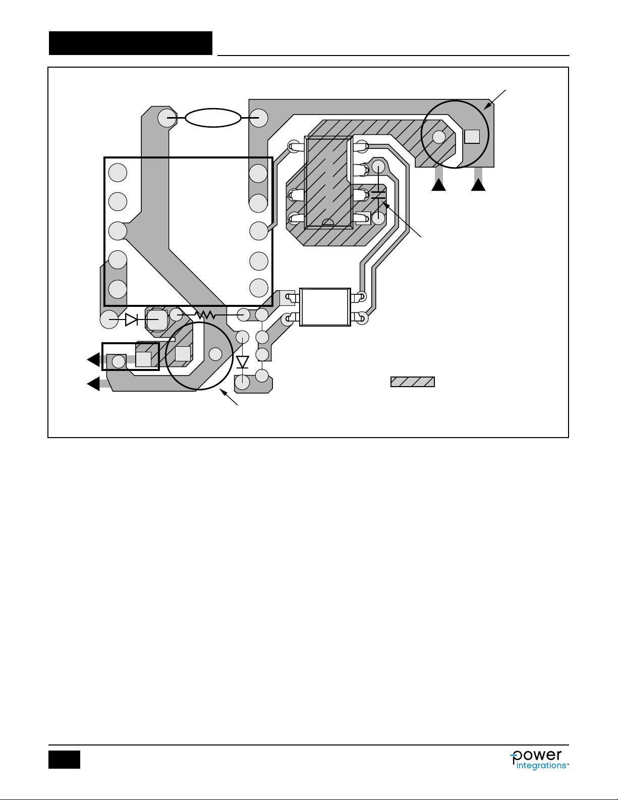
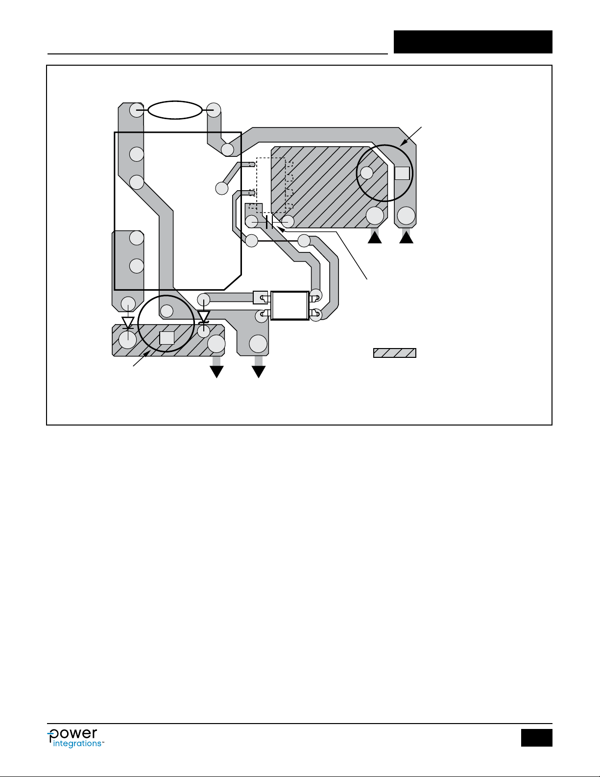
See Figure 6 for a recommended circuit board layout for
LinkSwitch-XT (P & G package).
Single Point Grounding
Use a single point ground connection from the input filter
capacitor to the area of copper connected to the SOURCE
pins.
www.power.com
5
Rev. H 10/20
Page 6
LNK362-364
OUT
PI-4155-102705
Input Filter
+
DC
-
TOP VIEW
Capacitor
T
r
a
n
s
f
o
r
m
e
r
Y1-
Capacitor
D
S
S
LinkSwitch-XT
Opto-
coupler
FB
S
BP
S
S
S
Maximize hatched copper
areas ( ) for optimum
heatsinking
HV DC
INPUT
C
BP
+
Output Filter
Capacitor
Figure 6. Recommended Printed Circuit Layout for LinkSwitch-XT using P Package in a Flyback Converter Conguration.
Bypass Capacitor C
BP
The BYPASS pin capacitor should be located as near as
possible to the BYPASS and SOURCE pins.
Primary Loop Area
The area of the primary loop that connects the input
filter capacitor, transformer primary and LinkSwitch-XT
together should be kept as small as possible.
Primary Clamp Circuit
A clamp is used to limit peak voltage on the DRAIN pin
at turn-off. This can be achieved by using an RCD clamp
or a Zener (~200 V) and diode clamp across the primary
winding. In all cases, to minimize EMI, care should
be taken to minimize the circuit path from the clamp
components to the transformer and LinkSwitch-XT.
Thermal Considerations
The copper area underneath the LinkSwitch-XT acts not
only as a single point ground, but also as a heatsink. As
this area is connected to the quiet source node, it should
be maximized for good heat sinking of LinkSwitch-XT.
The same applies to the cathode of the output diode.
6
Rev. H 10/20
Y-Capacitor
The placement of the Y-type cap should be directly from
the primary input filter capacitor positive terminal to the
common/return terminal of the transformer secondary.
Such a placement will route high magnitude commonmode surge currents away from the LinkSwitch-XT
device. Note that if an input pi (C, L, C) EMI filter is used,
then the inductor in the filter should be placed between
the negative terminals of the input filter capacitors.
Optocoupler
Place the optocoupler physically close to the LinkSwitch-XT
to minimize the primary-side trace lengths. Keep the high
current, high-voltage drain and clamp traces away from
the optocoupler to prevent noise pick up.
Output Diode
For best performance, the area of the loop connecting
the secondary winding, the output diode and the output
filter capacitor should be minimized. In addition, sufficient
copper area should be provided at the anode and
cathode terminals of the diode for heat sinking. A larger
www.power.com
Page 7
TOP VIEW
PI-4585-021607
Y1-
Capacitor
m
LNK362-364
Input Filter
Capacitor
LinkSwitch-XT
D
T
r
a
n
s
f
o
r
e
r
FB
BP
Opto-
coupler
S
S
S
S
-
+
HV DC
INPUT
C
BP
Maximize hatched copper
areas ( ) for optimum
heatsinking
Output Filter
Capacitor
Figure 7. Recommended Printed Circuit Layout for LinkSwitch-XT using D Package in a Flyback Conver ter Conguration.
area is preferred at the quiet cathode terminal. A large
anode area can increase high frequency radiated EMI.
+
DC
OUT
-
edge current spikes at start-up. Repeat under steady
state conditions and verify that the leading-edge current
spike event is below I
Quick Design Checklist
As with any power supply design, all LinkSwitch-XT
designs should be verified on the bench to make sure
that component specifications are not exceeded under
worst-case conditions. The following minimum set of
tests is strongly recommended:
1. Maximum drain voltage – Verify that VDS does not
exceed 650 V at the highest input voltage and peak
(overload) output power. The 50 V margin to the
700 V BV
variation, especially in clampless designs.
2. Maximum drain current – At maximum ambient
temperature, maximum input voltage and peak output
(overload) power, verify drain current waveforms for any
signs of transformer saturation and excessive leading-
specification gives margin for design
DSS
Under all conditions, the maximum drain current should
be below the specified absolute maximum ratings.
3. Thermal Check – At specified maximum output
power, minimum input voltage and maximum ambient
temperature, verify that the temperature specifications
are not exceeded for LinkSwitch-XT, transformer,
output diode and output capacitors. Enough thermal
margin should be allowed for part-to-part variation of
the R
of LinkSwitch-XT as specified in the data
DS(ON)
sheet. Under low line, maximum power, a maximum
LinkSwitch-XT SOURCE pin temperature of 105 °C is
recommended to allow for these variations.
Design Tools
Up-to-date information on design tools can be found at the
Power Integrations website: www.power.com
at the end of the t
LIMIT(MIN)
LEB(MIN)
.
www.power.com
7
Rev. H 10/20
Page 8
LNK362-364
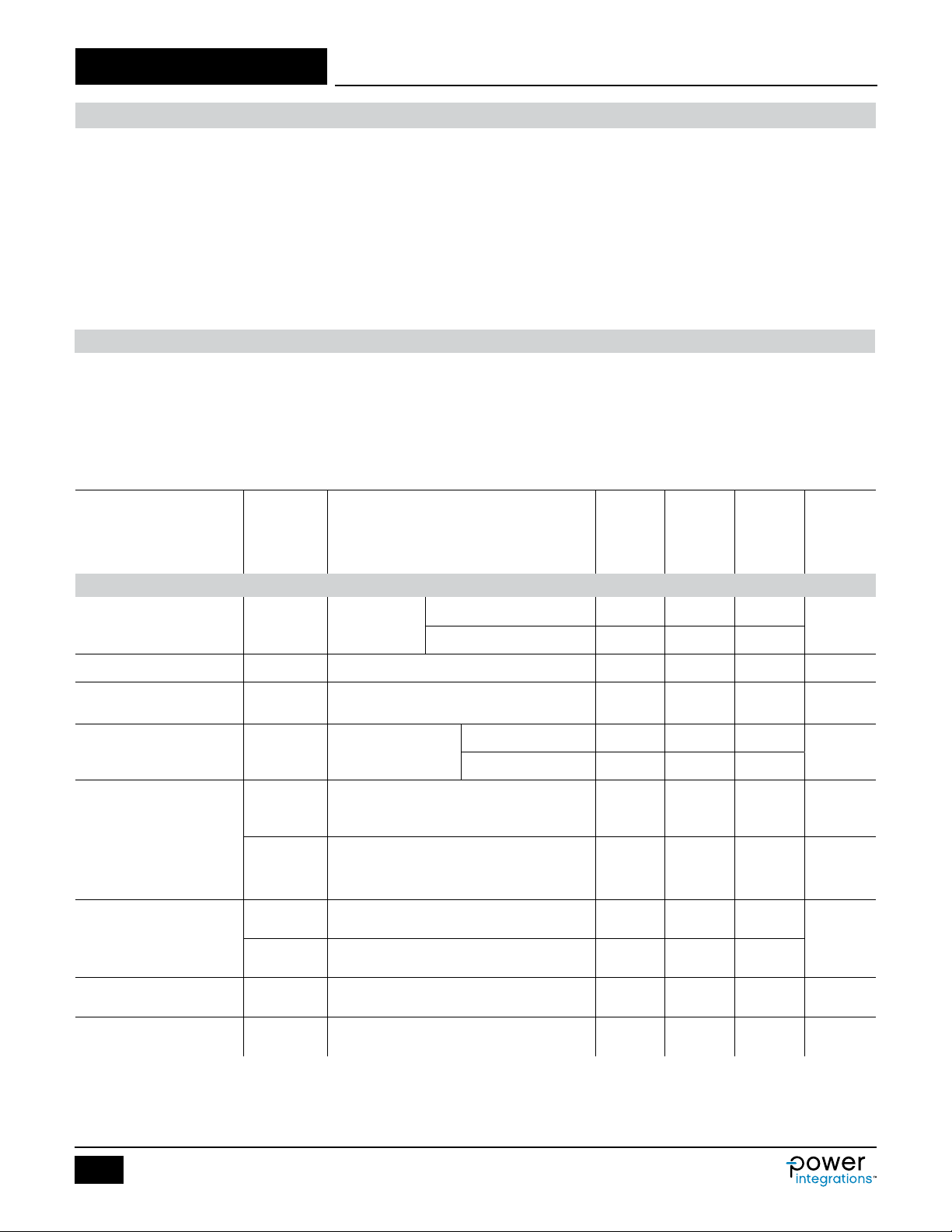
Absolute Maximum Ratings
(1,5)
DRAIN Pin Voltage .............................................-0.3 V to 700 V
Peak DRAIN Pin Current: LNK362................ 200 mA (375 mA)
....................................................................
LNK363/364......... 400 mA (750 mA)
FEEDBACK Pin Voltage ..........................................-0.3 V to 9 V
FEEDBACK Pin Current ................................................ 100 mA
BYPASS Pin Voltage................................................-0.3 V to 9 V
Storage Temperature ..................................... -65 °C to 150 °C
Operating Junction Temperature
Lead Temperature
(4)
....................................................... ..260 °C
(3)
.................. -40 °C to 150 °C
Thermal Resistance
Thermal Resistance: P or G Package:
(qJA) ........................... 70 °C/W
(1)
(qJC)
............................................... 11 °C/W
D Package:
(qJA) ..................... ......... 100 °C/W
(2)
(qJC)
............................................... 30 °C/W
(3)
; 60 °C/W
(3)
; 80 °C/W
(4)
Conditions
Parameter Symbol
SOURCE = 0 V; T
See Figure 8
(Unless Otherwise Specified)
Notes:
(2)
1. All voltages referenced to SOURCE, TA = 25 °C.
(2)
2. The higher peak DRAIN current is allowed while the DRAIN
voltage is simultaneously less than 400 V.
3. Normally limited by internal circuitry.
4. 1/16 in. from case for 5 seconds.
5. Maximum ratings specified may be applied, one at a time,
without causing permanent damage to the product.
Exposure to Absolute Maximum Rating conditions for
extended periods of time may affect product reliability.
Notes:
1. Measured on pin 2 (SOURCE) close to plastic interface.
2. Measured on pin 8 (SOURCE) close to plastic interface.
3. Soldered to 0.36 sq. in. (232 mm2), 2 oz. (610 g/m2) copper clad.
(4)
4. Soldered to 1 sq. in. (645 mm2), 2 oz. (610 g/m2) copper clad.
= -40 to 125 °C
J
Min Typ Max Units
Control Functions
Output Frequency f
Maximum Duty Cycle DC
FEEDBACK Pin Turn-Off
Threshold Current
FEEDBACK Pin Voltage
at Turn-Off Threshold
DRAIN Supply Current
BYPASS Pin
Charge Current
BYPASS Pin
Voltage
BYPASS Pin
Voltage Hysteresis
V
V
I
I
V
OSC
I
FB
I
S1
I
S2
CH1
CH2
BPH
FB
BP
MAX
TJ = 25 °C
S2 Open 60 %
TJ = 25 °C 30 49 68 µA
TJ = 0 °C to
125 °C
VFB ≥2 V
(MOSFET Not Switching)
See Note A
FEEDBACK Open
(MOSFET Switching)
See Notes A, B
VBP = 0 V, TJ = 25 °C
See Note C
VBP = 4 V, TJ = 25 °C
See Note C
Average 124 132 140
Peak-Peak Jitter 9
LNK362 1.55 1.65 1.75
LNK363-364 1.53 1.63 1.73
200 250 µA
250 300 µA
-5.5 -3.5 -1.8
-3.8 -2.3 -1.0
5.55 5.8 6.10 V
0.8 1.0 1.2 V
kHz
V
mA
8
Rev. H 10/20
www.power.com
Page 9
Parameter Symbol
Control Functions (cont)
Conditions
SOURCE = 0 V; T
See Figure 8
= -40 to 125 °C
J
(Unless Otherwise Specified)
LNK362-364
Min Typ Max Units
BYPASS Pin
Supply Current
Circuit Protection
Current Limit
Power Coefficient I
Leading Edge
Blanking Time
Current Limit Delay t
(See Note
I
BPSC
I
LIMIT
E)
t
LEB
See Note D 68 µA
di/dt = 30 mA/µs
T
= 25 °C
J
di/dt = 42 mA/µs
T
= 25 °C
J
di/dt = 50 mA/µs
T
= 25 °C
J
di/dt = 30 mA/µs
T
= 25 °C
J
2
f
di/dt = 42 mA/µs
T
= 25 °C
J
di/dt = 50 mA/µs
T
= 25 °C
J
TJ = 25 °C
See Note F
TJ = 25 °C
ILD
See Note F
LNK362 130 140 150
LNK363 195 210 225
LNK364 233 250 268
LNK362 2199 2587
LNK363 4948 5821
LNK364 7425 8250
LNK362 300 375
LNK363/364 170 250
125 ns
A
mA
2
ns
Hz
Thermal Shutdown
Temperature
Thermal Shutdown
Hysteresis
Output
ON-State
Resistance
OFF-State Drain
Leakage Current
R
T
SD
T
SHD
DS(ON)
I
DSS
See Note G 75 °C
LNK362
ID = 14 mA
LNK363
ID = 21 mA
LNK364
ID = 25 mA
VBP = 6.2 V, VFB ≥2 V,
VDS = 560 V,
T
= 125 °C
J
135 142 150 °C
TJ = 25 °C 48 55
TJ = 100 °C 76 88
TJ = 25 °C 29 33
W
TJ = 100 °C 46 54
TJ = 25 °C 24 28
TJ = 100 °C 38 45
50 µA
www.power.com
9
Rev. H 10/20
Page 10
LNK362-364
Parameter Symbol
Output (cont)
Conditions
SOURCE = 0 V; T
= -40 to 125 °C
J
See Figure 8
(Unless Otherwise Specified)
Min Typ Max Units
Breakdown
Voltage
BV
DSS
VBP = 6.2 V, VFB ≥ 2 V,
See Note H, T
= 25 °C
J
700 V
DRAIN Supply Voltage 50 V
Output Enable Delay t
Output Disable
Setup Time
Auto-Restart
ON-Time
Auto-Restart
Duty Cycle
t
DC
t
DST
EN
TJ = 25 °C
AR
AR
See Note I
See Figure 10 10 µs
0.5 µs
LNK362 40
ms
LNK363-364 45
5 %
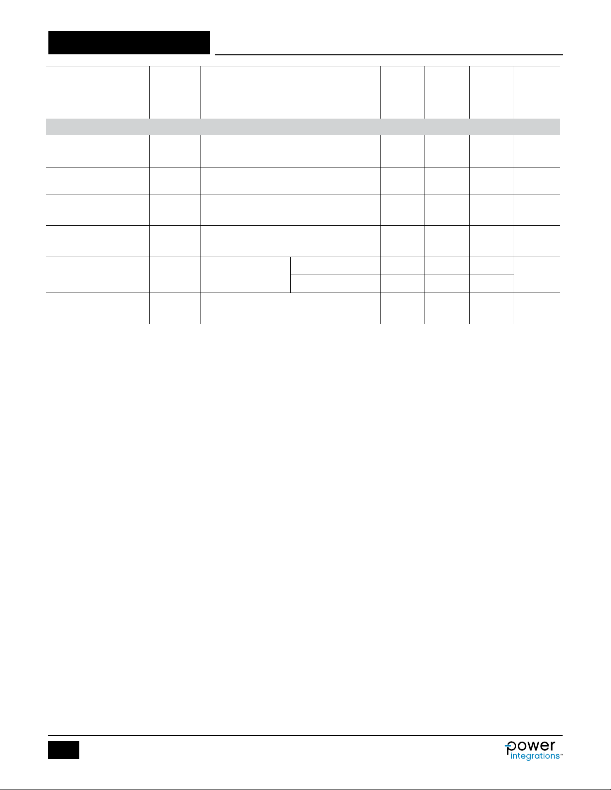
NOTES:
A. Total current consumption is the sum of IS1 and I
and the sum of IS2 and I
when FEEDBACK pin is shorted to SOURCE (MOSFET switching).
DSS
when FEEDBACK pin voltage is ≥2 V (MOSFET not switching)
DSS
B Since the output MOSFET is switching, it is difficult to isolate the switching current from the supply current at the
DRAIN. An alternative is to measure the BYPASS pin current at 6 V.
C. See Typical Performance Characteristics section Figure 15 for BYPASS pin start-up charging waveform.
D. This current is only intended to supply an optional optocoupler connected between the BYPASS and FEEDBACK
pins and not any other external circuitry.
E. For current limit at other di/dt values, refer to Figure 14.
F. This parameter is guaranteed by design.
G. This parameter is derived from characterization.
H. Breakdown voltage may be checked against minimum BV
but not exceeding minimum BV
DSS
.
specification by ramping the DRAIN pin voltage up to
DSS
I. Auto-restart on time has the same temperature characteristics as the oscillator (inversely proportional to frequency).
10
Rev. H 10/20
www.power.com
Page 11
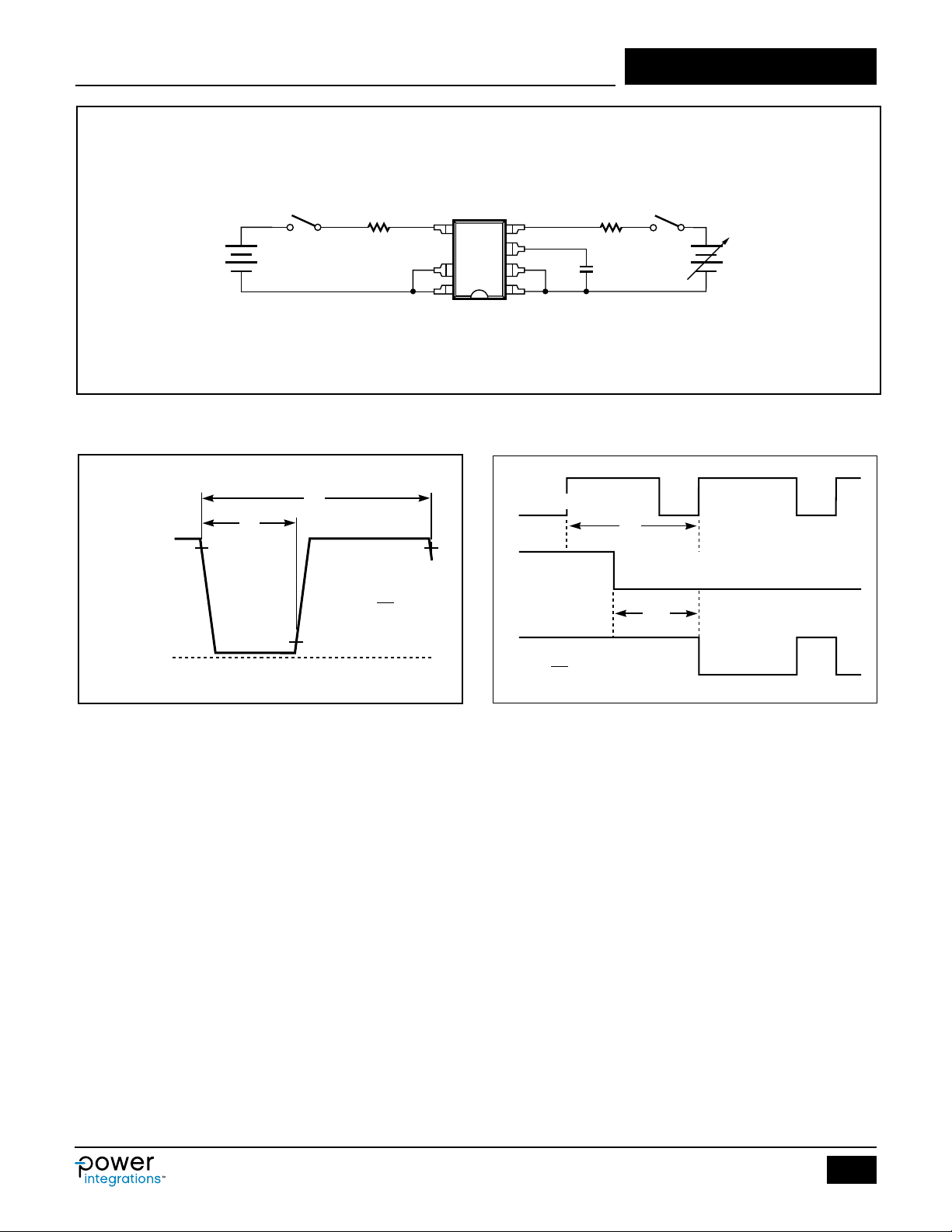
Figure 8. LinkSwitch-XT General Test Circuit.
PI-3490-060204
50 V50 V
D
FB
SS
S
S
BP
S1
470 kΩ
S2
0.1 µF
470 Ω
5 W
DRAIN
VOLTAGE
HV
0 V
PI-2048-021015
10%
90% 90%
t
1
t
2
D =
t
1
t
2
PI-3707-112503
FB
t
P
t
EN
DC
MAX
tP =
1
f
OSC
V
DRAIN
(internal signal)
LNK362-364
Figure 9. LinkSwitch-XT Dut y Cycle Measurement.
www.power.com
Figure 10. LinkSwitch-XT Output Enable Timing.
11
Rev. H 10/20
Page 12
LNK362-364
400
DRAIN Current (mA)
1.1
1.0
0.9
-50 -25 0 25 50 75 100 125 150
Junction Temperature (°C)
Breakdown Voltage
(Normalized to 25 °C)
PI-2213-012315
6
5
4
3
2
1
0
0 0.2 0.4 0.6 0.8 1.0
Time (ms)
PI-2240-012301
BYPASS Pin Voltage (V)
7
Current Limit
1.4
1.2
125
Normalized di/dt
PI-4092-081505
Normalized Current Limit
1.4
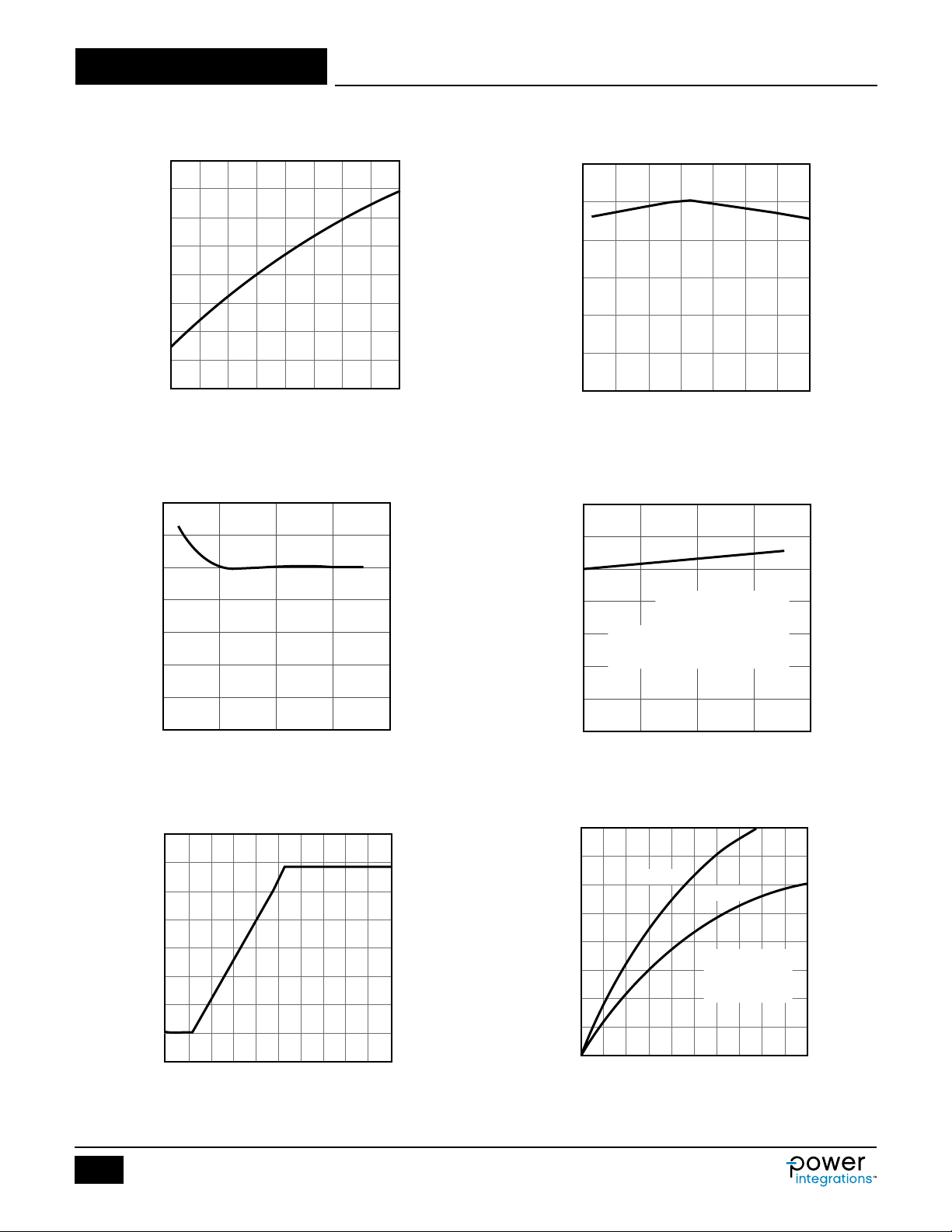
Typical Performance Characteristics
Figure 11. Breakdown vs. Temperature.
1.2
1.0
0.8
0.6
0.4
(Normalized to 25 °C)
0.2
PI-4091-081505
1.0
0.8
0.6
0.4
Output Frequency
(Normalized to 25 °C)
0.2
0
-50 -25 0 25 50 75 100
Junction Temperature (°C)
Figure 12. Frequency vs. Temperature.
1.2
1.0
0.8
0.6
0.4
0.2
LNK362
LNK363
LNK364
Normalized
di/dt = 1
TBD
30 mA/µs
42 mA/µs
50 mA/µs
Normalized
Current
Limit = 1
140 mA
210 mA
250 mA
PI-2680-021809
0
-50 050 100 150
Figure 13. Current Limit vs. Temperature.
Figure 15. BYPASS Pin Start-up Waveform.
12
Rev. H 10/20
Temperature (°C)
0
12345
Figure 14. Current Limit vs. di/dt.
350
300
25 °C
100 °C
250
200
150
100
Scaling Factors:
LNK362 0.5
LNK363 0.8
LNK364 1.0
50
0
0 4286101214161820
DRAIN Voltage (V)
Figure 16. Output Characteristics.
PI-4093-081605
www.power.com
Page 13
Drain Voltage (V)
Drain Capacitance (pF)
PI-4094-081605
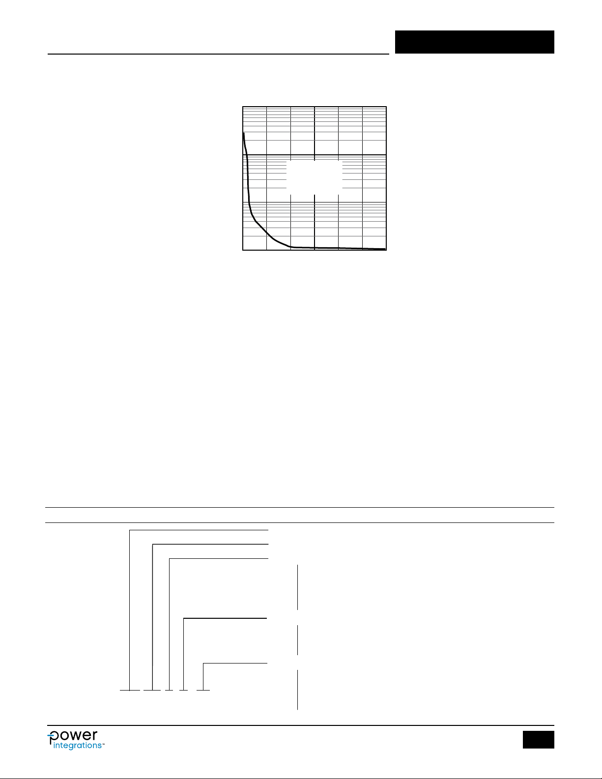
1000
Typical Performance Characteristics (cont.)
100
10
1
0 100 200 300 400 500 600
Scaling Factors:
LNK362 0.5
LNK363 0.8
LNK364 1.0
LNK362-364
Part Ordering Information
LNK 364 G N - TL
Figure 17. C
vs. Drain Voltage.
OSS
• LinkSwitch Product Family
• XT Series Number
• Package Identifier
Plastic Surface Mount DIP
G
Plastic DIP
P
Plastic SO-8
D
• Lead Finish
Pure Matte Tin (RoHS Compliant)
N
RoHS Compliant and Halogen Free (P and D package only)
G
• Tape & Reel and Other Options
Blank
Standard Configurations
Tape & Reel, 1 k pcs minimum for G Package. 2.5 k pcs for D
TL
Package. Not available for P Package.
www.power.com
13
Rev. H 10/20
Page 14
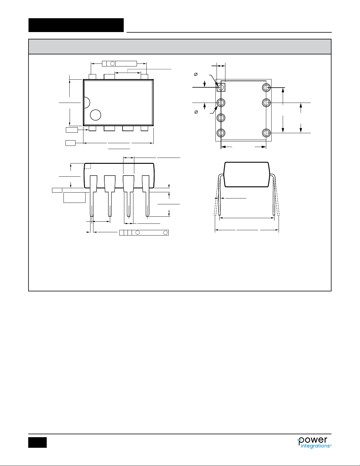
LNK362-364
-E-
.240 (6.10)
.260 (6.60)
Pin 1
⊕
D S
.004 (.10)
PDIP-8B (P Package)
.137 (3.48)
MINIMUM
.06 in
[1.41 mm]
∅
.03 in
[0.86 mm]
.10 in
[2.54 mm] Typ
∅
.06 in
[1.41 mm]
.30 in
[7.62 mm]
0.200 in
[5.08 mm]
-D-
.125 (3.18)
.145 (3.68)
-TSEATING
PLANE
.100 (2.54) BSC
Notes:
1. Package dimensions conform to JEDEC specification MS-001-AB (Issue B 7/85) for standard dual-in-line (DIP) package with .300 inch row spacing.
2. Controlling dimensions are inches. Millimeter sizes are shown in parentheses.
3. Dimensions shown do not include mold flash or other protrusions. Mold flash or protrusions shall not exceed .006 (.15) on any side.
4. Pin locations start with Pin 1, and continue counter-clock-wise to Pin 8 when viewed from the top. The notch and/or dimple are aids in locating Pin 1.
Pin 6 is omitted.
5. Minimum metal to metal spacing at the package body for the omitted lead location is .137 inch (3.48 mm).
6. Lead width measured at package body.
7. Lead spacing measured with the leads constrained to be perpendicular to plane T.
.356 (9.05)
.387 (9.83)
.014 (.36)
.022 (.56)
⊕
T E D S
.048 (1.22)
.068 (1.73)
.010 (.25) M
.057 (1.45)
.068 (1.73)
(NOTE 6)
.015 (.38)
MINIMUM
.118 (3.00)
.140 (3.56)
.30 in
[7.62 mm]
.008 (.20)
.015 (.38)
.300 (7.62) BSC
(NOTE 7)
.300 (7.62)
.390 (9.91)
P08B
PI-2551b-092920
14
Rev. H 10/20
www.power.com
Page 15
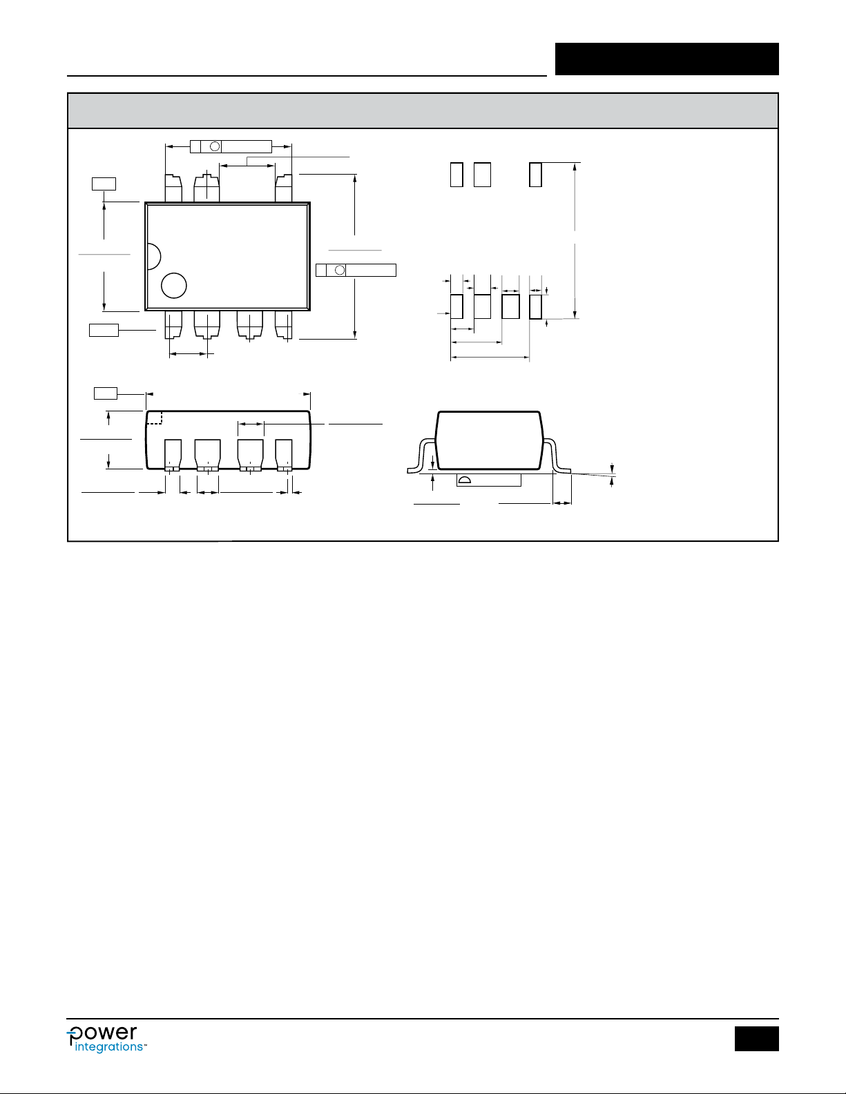
-E-
.240 (6.10)
.260 (6.60)
Pin 1
-D-
.125 (3.18)
.145 (3.68)
D S
.004 (.10)
⊕
.100 (2.54) (BSC)
.356 (9.05)
.387 (9.83)
SMD-8B (G Package)
.137 (3.48)
MINIMUM
.372 (9.45)
.388 (9.86)
.010 (.25)
E S
⊕
.057 (1.45)
.068 (1.73)
(NOTE 5)
.046
Pin 1
.086
.186
Solder Pad Dimensions
.060
.286
.060
.046
.080
LNK362-364
Notes:
1. Controlling dimensions are
inches. Millimeter sizes are
shown in parentheses.
2. Dimensions shown do not
include mold flash or other
protrusions. Mold flash or
protrusions shall not exceed
.006 (.15) on any side.
.420
3. Pin locations start with Pin 1,
and continue counter-clock wise to Pin 8 when viewed
from the top. Pin 6 is omitted.
4. Minimum metal to metal
spacing at the package body
for the omitted lead location
is .137 inch (3.48 mm).
5. Lead width measured at
package body.
6. D and E are referenced
datums on the package body.
.032 (.81)
.043 (1.09)
.048 (1.22)
.068 (1.73)
.009 (.23)
.004 (.10)
.012 (.30)
.004 (.10)
.036 (0.91)
.044 (1.12)
0 -
°
°
8
G08B
PI-2546a-092920
www.power.com
15
Rev. H 10/20
Page 16
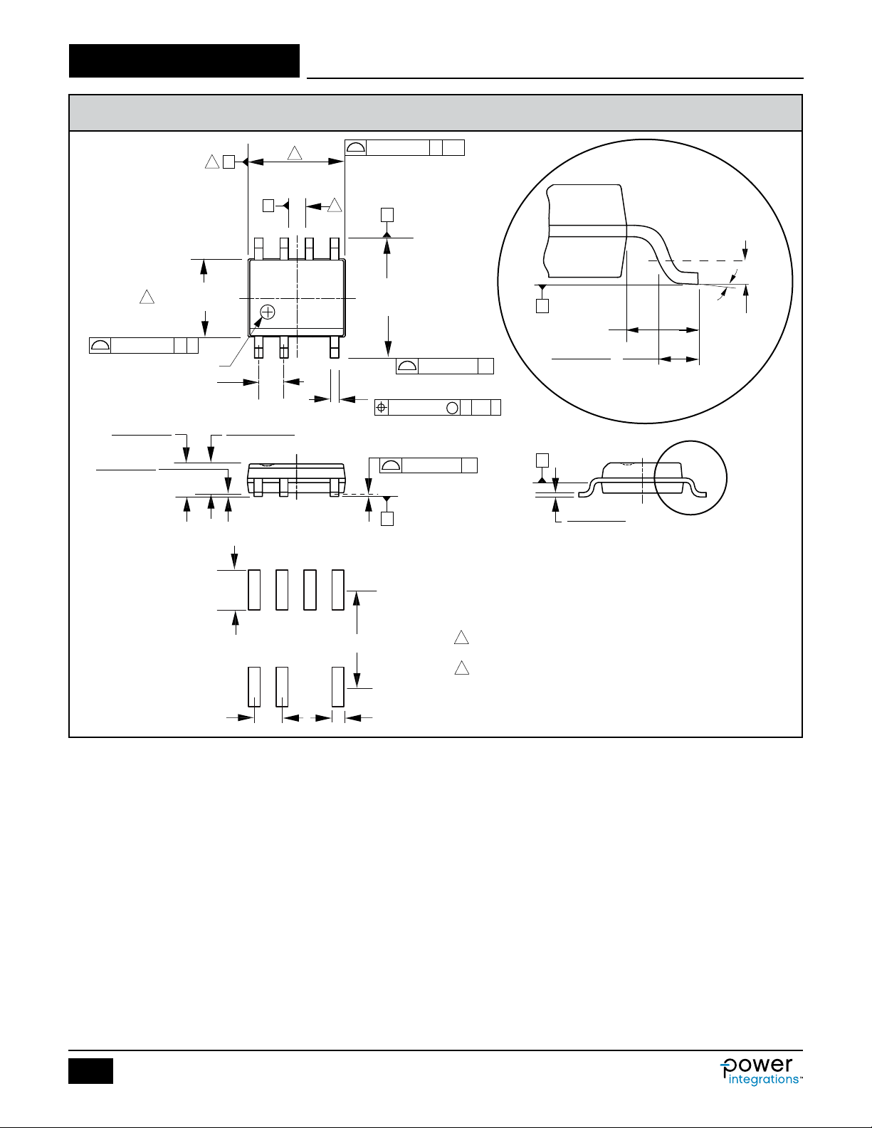
LNK362-364
SO-8C (D Package)
0.10 (0.004)
2X
1.35 (0.053)
1.75 (0.069)
0.10 (0.004)
0.25 (0.010)
3.90 (0.154) BSC
2
D
C
Pin 1 ID
1.27 (0.050) BSC
B
4
1.25 - 1.65
(0.049 - 0.065)
2
4.90 (0.193) BSC
A
8
1
4
5
4
0.10 (0.004)
D
6.00 (0.236) BSC
2X
7X 0.31 - 0.51 (0.012 - 0.020)
0.25 (0.010)
7X
SEATING PLANE
C
A-B
C
0.20 (0.008)
M
0.10 (0.004)
2X
C A-B D
C
C
SEATING
PLANE
1.04 (0.041) REF
C
0.40 (0.016)
1.27 (0.050)
H
0.17 (0.007)
0.25 (0.010)
DETAIL A
o
0 - 8
0.25 (0.010)
BSC
DETAIL A
GAUGE
PLANE
D07C
Reference
Solder Pad
Dimensions
1.27 (0.050)
2.00 (0.079)
+
Notes:
1. JEDEC reference: MS-012.
4.90 (0.193)
+
+
+
0.60 (0.024)
2. Package outline exclusive of mold flash and metal burr.
3. Package outline inclusive of plating thickness.
4. Datums A and B to be determined at datum plane H.
5. Controlling dimensions are in millimeters. Inch dimensions
are shown in parenthesis. Angles in degrees.
PI-4526-040110
16
Rev. H 10/20
www.power.com
Page 17

LNK362-364
Revision Notes Date
B Released Final Data Sheet. 11/05
C Corrected Application Example section. 12/05
D Added SO-8C package. 2/07
E Updated Part Ordering Information section with Halogen Free 11/08
F Updated with new Brand Style. 05/15
G
H
Updated PDIP-8B (P Package) and SMD-8B (G Package) per PCN-16232.
Updated package drawings PDIP-8B and SMD-8B.
08/16
10/20
www.power.com
17
Rev. H 10/20
Page 18

LNK362-364
For the latest updates, visit our website: www.power.com
Power Integrations reserves the right to make changes to its products at any time to improve reliability or manufacturability. Power Integrations
does not assume any liability arising from the use of any device or circuit described herein. POWER INTEGRATIONS MAKES NO WARR ANTY
HEREIN AND SPECIFICALLY DISCLAIMS ALL WARRANTIES INCLUDING, WITHOUT LIMITATION, THE IMPLIED WARRANTIES OF MERCHANTABILIT Y,
FITNESS FOR A PARTICULAR PURPOSE, AND NON-INFRINGEMENT OF THIRD PARTY RIGHTS.
Patent Information
The products and applications illustrated herein (including transformer construction and circuits external to the products) may be covered by one
or more U.S. and foreign patents, or potentially by pending U.S. and foreign patent applications assigned to Power Integrations. A complete list of
Power Integrations patents may be found at www.power.com. Power Integrations grants its customers a license under certain patent rights as set
forth at www.power.com/ip.htm.
Life Support Policy
POWER INTEGRATIONS PRODUCTS ARE NOT AUTHORIZED FOR USE AS CRITICAL COMPONENTS IN LIFE SUPPORT DEVICES OR SYSTEMS
WITHOUT THE EXPRESS WRITTEN APPROVAL OF THE PRESIDENT OF POWER INTEGRATIONS. As used herein:
1. A Life support device or system is one which, (i) is intended for surgical implant into the body, or (ii) supports or sustains life, and (iii) whose
failure to perform, when properly used in accordance with instructions for use, can be reasonably expected to result in signicant injury or
death to the user.
2. A critical component is any component of a life support device or system whose failure to perform can be reasonably expected to cause the
failure of the life support device or system, or to affect its safety or effectiveness.
Power Integrations, the Power Integrations logo, CAPZero, ChiPhy, CHY, DPA-Switch, EcoSmart, E-Shield, eSIP, eSOP, HiperPLC, HiperPFS,
HiperTFS, InnoSwitch, Innovation in Power Conversion, InSOP, LinkSwitch, LinkZero, LYTSwitch, SENZero, TinySwitch, TOPSwitch, PI, PI Expert,
PowiGaN, SCALE, SCALE-1, SCALE-2, SCALE-3 and SCALE-iDriver, are trademarks of Power Integrations, Inc. Other trademarks are property of
their respective companies. ©2020, Power Integrations, Inc.
Power Integrations Worldwide Sales Support Locations
World Headquarters
5245 Hellyer Avenue
San Jose, CA 95138, USA
Main: +1-408-414-9200
Customer Service:
Worldwide: +1-65-635-64480
Americas: +1-408-414-9621
e-mail: [email protected]
China (Shanghai)
Rm 2410, Charity Plaza, No. 88
North Caoxi Road
Shanghai, PRC 200030
Phone: +86-21-6354-6323
e-mail: [email protected]
China (Shenzhen)
17/F, Hivac Building, No. 2, Keji Nan
8th Road, Nanshan District,
Shenzhen, China, 518057
Phone: +86-755-8672-8689
e-mail: [email protected]
18
Rev. H 10/20
Germany (AC-DC/LED Sales)
Einsteinring 24
85609 Dornach/Aschheim
Germany
Tel: +49-89-5527-39100
e-mail: [email protected]
Germany (Gate Driver Sales)
HellwegForum 1
59469 Ense
Germany
Tel: +49-2938-64-39990
e-mail: [email protected]
India
#1, 14th Main Road
Vasanthanagar
Bangalore-560052 India
Phone: +91-80-4113-8020
e-mail: [email protected]
Italy
Via Milanese 20, 3rd. Fl.
20099 Sesto San Giovanni (MI) Italy
Phone: +39-024-550-8701
e-mail: [email protected]
Japan
Yusen Shin-Yokohama 1-chome Bldg.
1-7-9, Shin-Yokohama, Kohoku-ku
Yokohama-shi,
Kanagawa 222-0033 Japan
Phone: +81-45-471-1021
e-mail: [email protected]
Korea
RM 602, 6FL
Korea City Air Terminal B/D, 159-6
Samsung-Dong, Kangnam-Gu,
Seoul, 135-728, Korea
Phone: +82-2-2016-6610
e-mail: [email protected]
Singapore
51 Newton Road
#19-01/05 Goldhill Plaza
Singapore, 308900
Phone: +65-6358-2160
e-mail: [email protected]
Taiwan
5F, No. 318, Nei Hu Rd., Sec. 1
Nei Hu Dist.
Taipei 11493, Taiwan R.O.C.
Phone: +886-2-2659-4570
e-mail: [email protected]
UK
Building 5, Suite 21
The Westbrook Centre
Milton Road
Cambridge
CB4 1YG
Phone: +44 (0) 7823-557484
e-mail: [email protected]
www.power.com
 Loading...