

CM100TJ-12F
Powerex, Inc., 200 Hillis Street, Youngwood, Pennsylvania 15697-1800 (724) 925-7272
A
D
F
19
20
Tc
J
B
21
L
C
21
1
2
3
4
20
19
S
2
1
P
E
G
NOT
CONNECTED
17
T
4
3
5
6
7
Q
Y
X
5
6
7
8
17 15
CONNECTED
1618
8
10
11
12
NOT
9
9
H
15
14
M
N
13
10
12
11
R
13
14
U
K
Tc
L
W
V
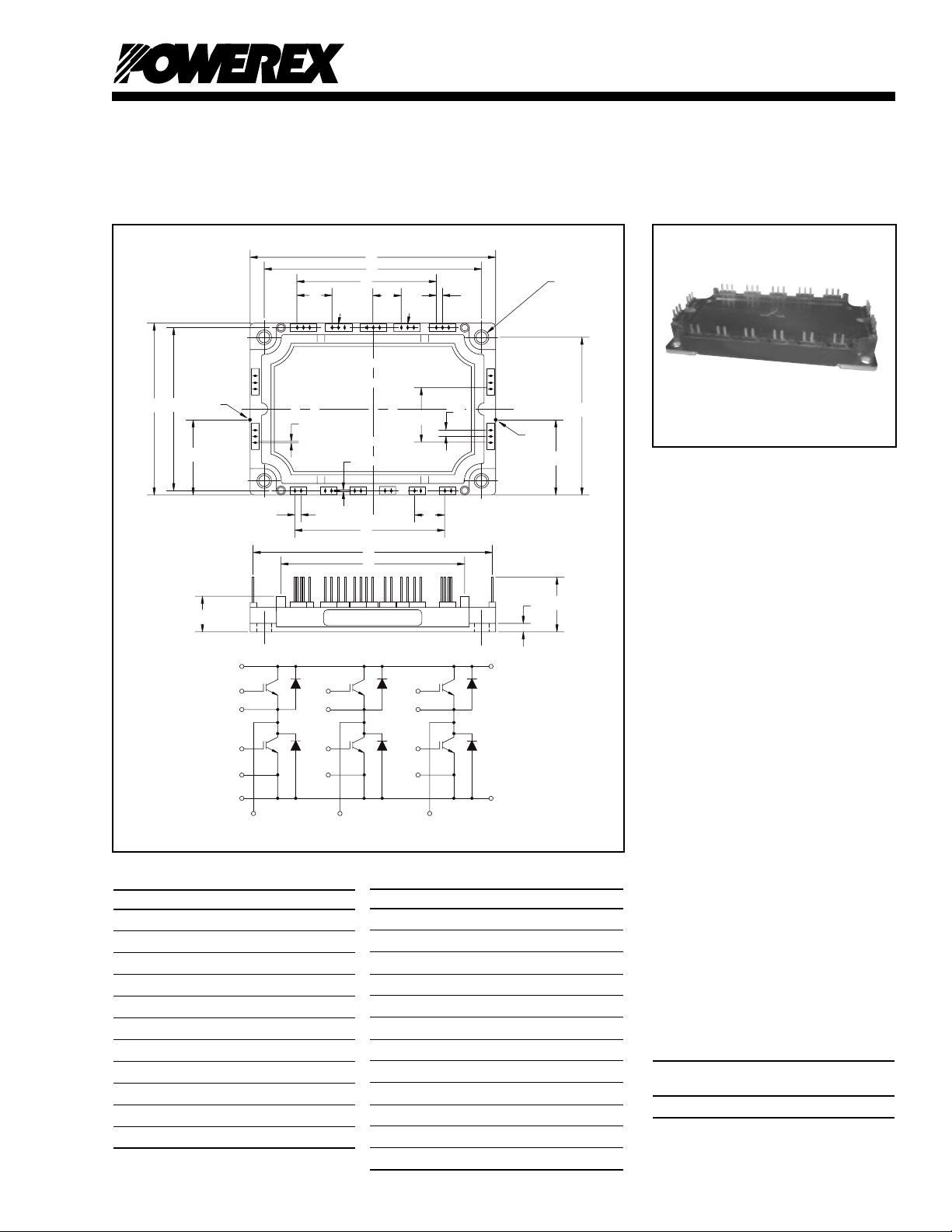
Trench Gate Design
Six IGBTMOD™
100 Amperes/ 600 Volts
Description:
Powerex IGBTMOD™ Modules
are designed for use in switching
applications. Each module consists
of six IGBT Transistors in a three
phase bridge configuration, with
each transistor having a reverseconnected super-fast recover y
free-wheel diode. All components
and interconnects are isolated
from the heat sinking baseplate,
offering simplified system assembly
and thermal management.
Features:
□ Low Drive Power
□ Low V
□ Discrete Super-Fast Recovery
□ Isolated Baseplate for Easy
CE(sat)
Free-Wheel Diode
Heat Sinking
Outline Drawing and Circuit Diagram
Dimensions Inches Millimeters
A 4.78 121.5
B 2.42 61.5
C 0.67 17.0
D 4.33±0.01 110.0±0.25
E 3.00 76.2
F 0.75 19.05
G 0.60 15.24
H 0.15 3.81
J 2.26 57.5
K 1.97±0.01 50.0±0.25
L 1.07 27.0
Dimensions Inches Millimeters
M 0.15 3.81
N 0.75 19.05
P 0.15 3.81
Q 3.00 76.2
R 0.60 15.24
S 0.45 1.15
T 0.04 1.0
U 0.22 Dia. 5.5 Dia.
V 0.12 3.0
W 0.81 20.5
X 3.72 94.5
Y 4.62 118.11
Applications:
□ AC Motor Control
□ UPS
□ Battery Powered Supplies
Ordering Information:
Example: Select the complete
module number you desire from
the table - i.e. CM100TJ-12F is a
600V (V
), 100 Ampere Six-
CES
IGBT IGBTMOD™ Power Module.
Current Rating V
Type Amperes Volts (x 50)
CM 100 12
CES
1
1

Powerex, Inc., 200 Hillis Street, Youngwood, Pennsylvania 15697-1800 (724) 925-7272
CM100TJ-12F
Trench Gate Design Six IGBTMOD™
100 Amperes/600 Volts
Absolute Maximum Ratings, Tj = 25 °C unless otherwise specified
Ratings Symbol CM100TJ-12F Units
Junction Temperature T
Storage Temperature T
Collector-Emitter Voltage (G-E SHORT) V
Gate-Emitter Voltage (C-E SHORT) V
Collector Current (Tc = 25°C) I
Peak Collector Current (Tj ≤ 150°C) I
Emitter Current (Tc = 25°C)** I
Peak Emitter Current** I
Maximum Collector Dissipation (Tj < 150°C) (Tc = 25°C) P
j
stg
CES
GES
C
CM
E
EM
c
-40 to 150 °C
-40 to 125 °C
600 Volts
±20 Volts
100 Amperes
200* Amperes
100 Amperes
200* Amperes
290 Watts
Mounting Torque, M5 Mounting – 31 in-lb
Weight – 300 Grams
Isolation Voltage (Main Terminal to Baseplate, AC 1 min.) V
iso
2500 Volts
Static Electrical Characteristics, Tj = 25 °C unless otherwise specified
Characteristics Symbol Test Conditions Min. Typ. Max. Units
Collector-Cutoff Current I
Gate Leakage Current I
Gate-Emitter Threshold Voltage V
Collector-Emitter Saturation Voltage V
Total Gate Charge Q
Emitter-Collector Voltage** V
* Pulse width and repetition rate should be such that the device junction temperature (Tj) does not exceed T
** Represents characteristics of the anti-parallel, emitter-to-collector free-wheel diode (FWDi).
CES
GES
GE(th)
CE(sat)
G
EC
VCE = V
VGE = V
, VGE = 0V – – 1 mA
CES
, VCE = 0V – – 20 µA
GES
IC = 10mA, VCE = 10V 5 6 7 Volts
IC = 100A, VGE = 15V, Tj = 25°C– 1.6 2.2 Volts
IC = 100A, VGE = 15V, Tj = 125°C– 1.6 – Volts
VCC = 300V, IC = 100A, VGE = 15V – 620 – nC
IE = 100A, VGE = 0V – – 2.6 Volts
rating.
j(max)
2
2

Powerex, Inc., 200 Hillis Street, Youngwood, Pennsylvania 15697-1800 (724) 925-7272
CM100TJ-12F
Trench Gate Design Six IGBTMOD™
100 Amperes/600 Volts
Dynamic Electrical Characteristics, Tj = 25 °C unless otherwise specified
Characteristics Symbol Test Conditions Min. Typ. Max. Units
Input Capacitance C
Output Capacitance C
Reverse Transfer Capacitance C
Inductive Turn-on Delay Time t
d(on)
Load Rise Time t
Switch Turn-off Delay Time t
d(off)
Times Fall Time t
Diode Reverse Recovery Time** t
Diode Reverse Recovery Charge** Q
ies
oes
res
r
f
rr
rr
VCE = 10V, VGE = 0V – – 1.8 nf
VCC = 300V, – – 100 ns
IC = 100A, – – 80 ns
V
= V
GE1
= 15V, – – 300 ns
GE2
RG = 6.3⍀,––250 ns
Inductive Load – – 150 ns
Switching Operation – 1.9 – µC
––27nf
––1nf
Thermal and Mechanical Characteristics, Tj = 25 °C unless otherwise specified
Characteristics Symbol Test Conditions Min. Typ. Max. Units
Thermal Resistance, Junction to Case R
Thermal Resistance, Junction to Case R
Thermal Resistance, Junction to Case R
Thermal Resistance, Junction to Case Rth(j-c)'D Per FWDi 1/6 Module, Tc Reference – 0.37 – °C/W
Contact Thermal Resistance R
** Represents characteristics of the anti-parallel, emitter-to-collector free-wheel diode (FWDi).
QPer IGBT 1/6 Module, Tc Reference – – 0.43 °C/W
th(j-c)
Point per Outline Drawing
DPer FWDi 1/6 Module, Tc Reference – – 0.70 °C/W
th(j-c)
Point per Outline drawing
'Q Per IGBT 1/6 Module, – 0.28 – °C/W
th(j-c)
Tc Reference Point Under Chip
Tc Reference Point Under Chip
th(c-f)
Per Module, Thermal Grease Applied – 0.13 – °C/W
3
Powerex, Inc., 200 Hillis Street, Youngwood, Pennsylvania 15697-1800 (724) 925-7272
CM100TJ-12F
Trench Gate Design Six IGBTMOD™
100 Amperes/600 Volts
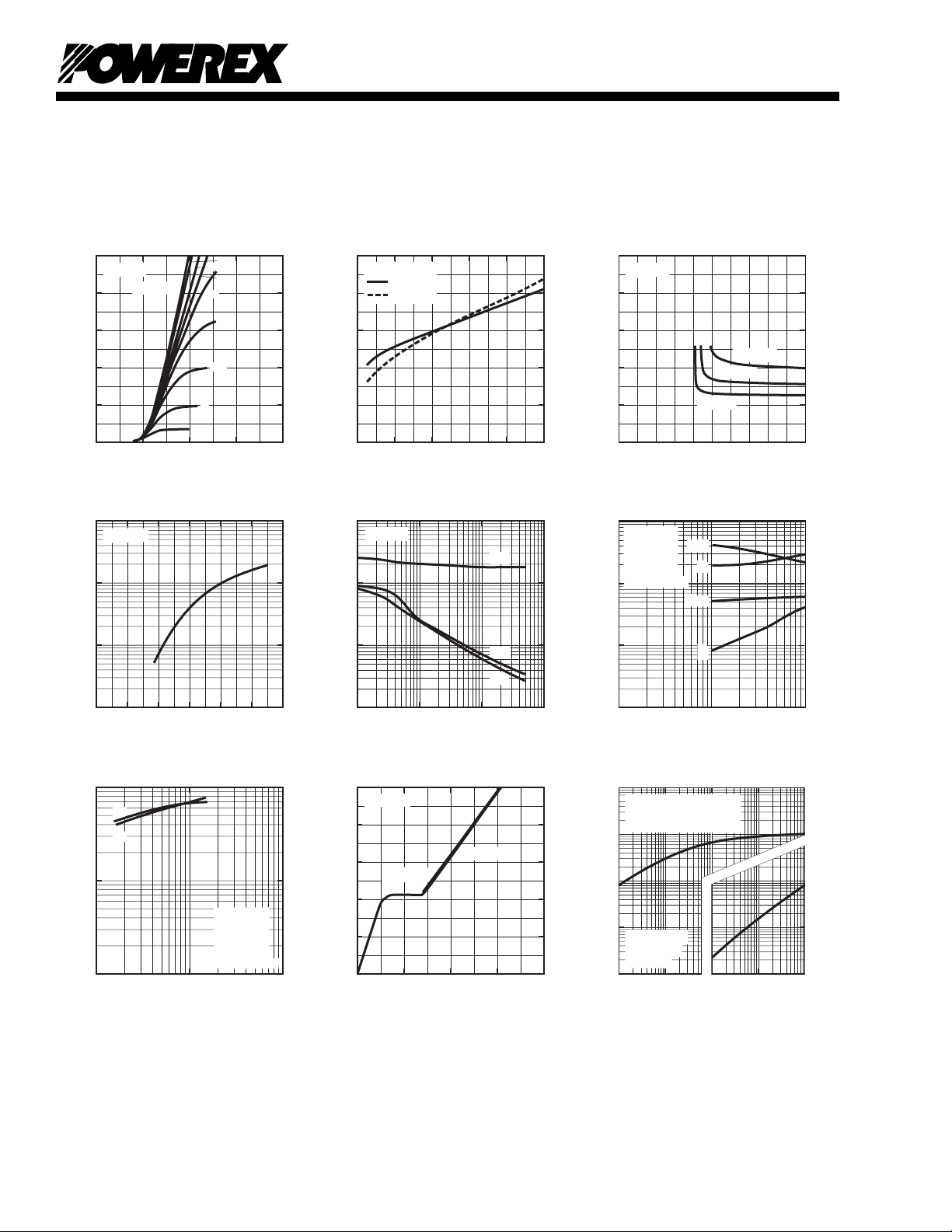
OUTPUT CHARACTERISTICS
(TYPICAL)
200
160
, (AMPERES)
C
120
Tj = 25
o
C
VGE = 20V
80
40
COLLECTOR CURRENT, I
0
01234
COLLECTOR-EMITTER VOLTAGE, VCE, (VOLTS)
FREE-WHEEL DIODE
FORWARD CHARACTERISTICS
3
10
(TYPICAL)
7.5
15
11
10
9.5
9
8.5
8
Tj = 25°C
2
10
, (AMPERES)
E
1
10
EMITTER CURRENT, I
0
10
0 0.5 1.0 1.5 2.52.0 3.0
EMITTER-COLLECTOR VOLTAGE, V
REVERSE RECOVERY CHARACTERISTICS
2
10
I
rr
, (ns)
rr
REVERSE RECOVERY TIME, t
t
rr
1
10
0
10
1
10
(TYPICAL)
2
EMITTER CURRENT, IE, (AMPERES)
10
, (VOLTS)
EC
VCC = 300V
V
= ±15V
GE
R
= 4.2 Ω
G
T
= 25°C
j
Inductive Load
SATURATION VOLTAGE CHARACTERISTICS
2.5
2.0
, (VOLTS)
CE(sat)
1.5
1.0
COLLECTOR-EMITTER
0.5
SATURATION VOLTAGE, V
0
2
10
, (nF)
res
1
, C
10
oes
, C
ies
0
10
CAPACITANCE, C
-1
10
10
2
10
20
16
, (AMPERES)
, (VOLTS)
rr
GE
12
1
10
8
4
GATE-EMITTER VOLTAGE, V
0
REVERSE RECOVERY CURRENT, I
10
3
10
0
COLLECTOR-EMITTER
(TYPICAL)
VGE = 15V
Tj = 25°C
= 125°C
T
j
04080120 160
COLLECTOR-CURRENT, IC, (AMPERES)
CAPACITANCE VS. V
(TYPICAL)
CE
VGE = 0V
C
ies
C
oes
C
res
-1
COLLECTOR-EMITTER VOLTAGE, VCE, (VOLTS)
0
10
GATE CHARGE, V
1
10
GE
IC = 150A
VCC = 300V
VCC = 200V
400 800 16001200
0
GATE CHARGE, QG, (nC)
200
10
SATURATION VOLTAGE CHARACTERISTICS
5
4
, (VOLTS)
CE(sat)
3
COLLECTOR-EMITTER
(TYPICAL)
Tj = 25°C
2
COLLECTOR-EMITTER
1
SATURATION VOLTAGE, V
0
048121620
GATE-EMITTER VOLTAGE, VGE, (VOLTS)
HALF-BRIDGE
SWITCHING CHARACTERISTICS
3
10
VCC = 300V
V
GE
R
= 6.3 Ω
G
T
= 125°C
j
2
Inductive Load
10
1
10
SWITCHING TIME, (ns)
0
10
2
0
10
COLLECTOR CURRENT, IC, (AMPERES)
IMPEDANCE CHARACTERISTICS
10-310
1
th(j-c)
10
R
th(j-c)
Under Chip = 0.28°C/W
R
th(j-c)
0
10
-1
10
• (NORMALIZED VALUE)
th
-2
10
= R
th
Per Unit Base
Z
Single Pulse
T
= 25°C
C
-3
10
NORMALIZED TRANSIENT THERMAL IMPEDANCE, Z
(TYPICAL)
t
= ±15V
d(off)
t
d(on)
TRANSIENT THERMAL
(IGBT & FWDi)
-2
= 0.43°C/W (IGBT)
= 0.7°C/W (FWDi)
TIME, (s)
IC = 100A
IC = 40A
t
f
t
r
1
10
-1
10
-5
10
IC = 200A
0
10
-4
10
2
10
1
10
-1
10
-2
10
-3
10
-3
10
4
 Loading...