

Page 1
IN
AOTION
SEMICONDUCTORS
The General Electric
signed for
power
C444
switching
and
C445 Silicon Controlled Rectifiers are de-
at
high frequencies. These are all-diffused Press-
Pak devices employing the field-proven interdigitated amplifying gate system.
FEATURES:
..
Interdigitated gate
structure
to
maximize high frequency current switching
capability.
Fully characterized for
..
High
di/dt
ratings.
..
High dv/dt capability
Guaranteed maximum
..
Rugged hermetic glazed ceramic package having 1" creepage path.
operation
with
turn-off
'"
~
w
~
'"
~
z
~
n:
::J
u
W
II-
'"
'?
z
0
'"
w
'"
u.
in inverter applications.
selections available.
time
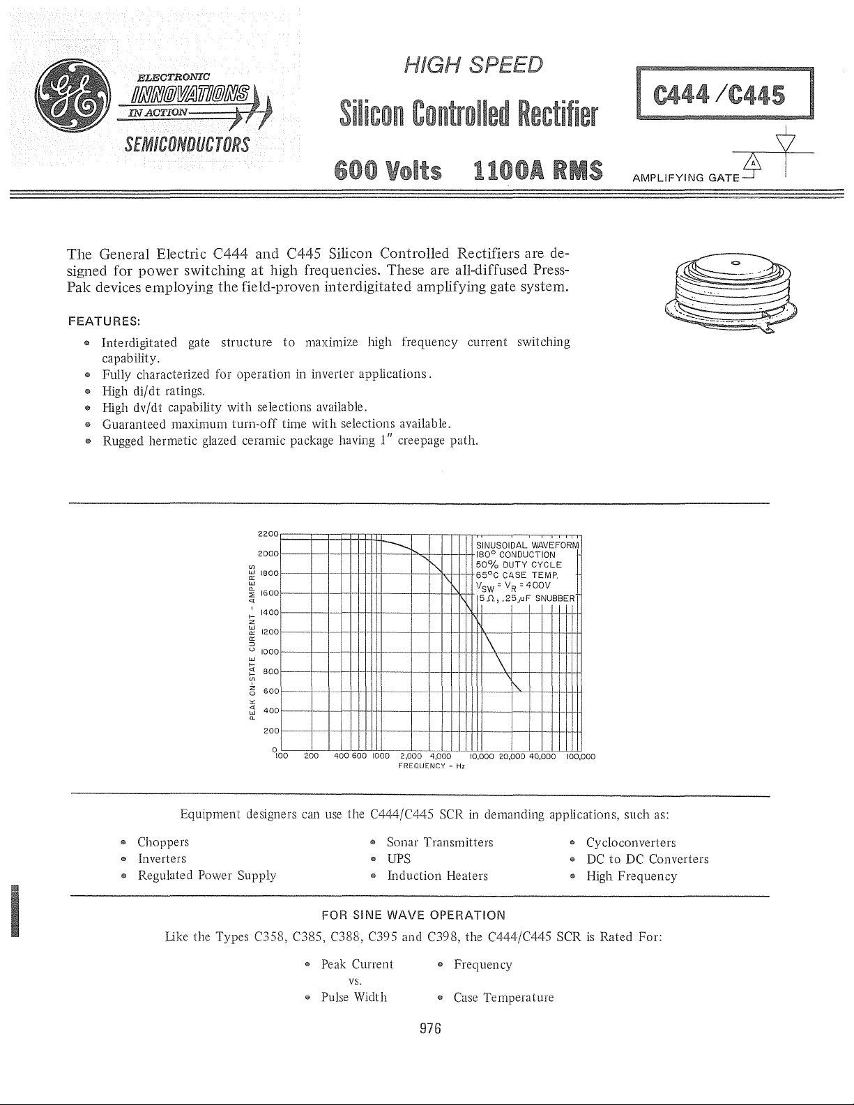
2200
2000
1800
1600
1400
1200
!----
1000
800
600
400
200
with
selections available.
c--L
-
I
--
0-
SINUSOIDAL
180°
CONDUCTION
50%
65°C
vsw
5Jl.,
= vR =
.25jJF
t\
-~
WAVEFORM
DUTY CYCLE
CASE TEMP.
400V
SNUBBER
- -
f'....
t-
~oo
200
400
600
1000
2,000
4,000
10,000
20,000
FREQUENCY
- Hz
40,000
100,000
AMPLIFYING
GAT*
I
Equipment designers
" Choppers
" Inverters
" Regulated Power Supply
Uke
the Types C358, C385, C388, C395 and C398,
C~U1
use the C444/C445 SCR in demanding applications, such as:
" Sonar Transmitters
€I
UPS
" Induction Heaters
FOR SINE WAVE OPERATION
" Peak Current
" Frequency
the
C444/C445 SCR
" Cycloconverters
..
DC
to
" High
is
Rated For:
vs.
" Pulse Width
" Case Tempera lure
976
DC Converters
Frequency
Page 2
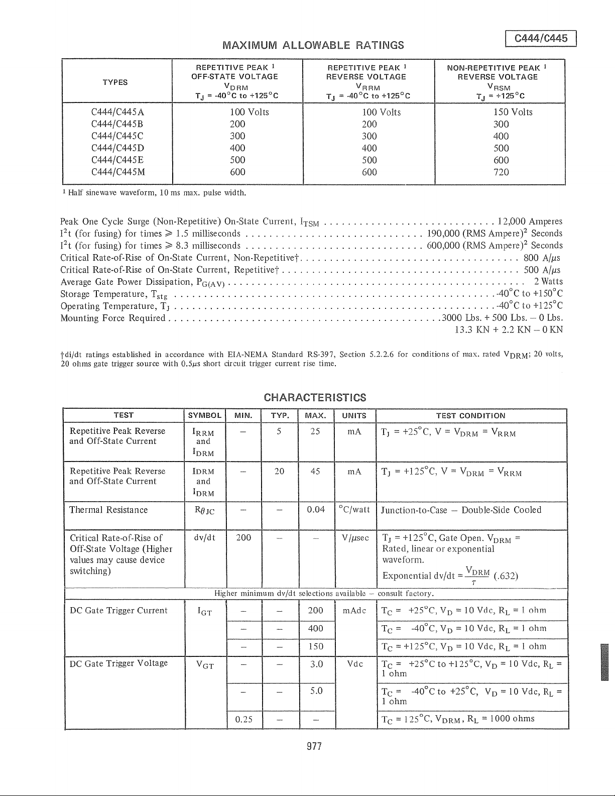
MAXIMUM
ALLOWABLE RATINGS
C444/C445
TYPES
C444/C445A
C444/C445B
C444/C445C
C444/C445D
C444/C445E
C444/C445M
1 Half
sinewave
Peak One Cycle Surge
I2t
(for
et
(for
Critical Rate-of-Rise
Critical Rate-of-Rise
Average
Storage
Operating
Mounting
tdi/dt
ratings established
20
ohms gate trigger source with
waveform,
fusing)
fusing)
Temperature,
for
for
Gate
Power
Temperature,
Force
Required
times;;;'
times;;;'
of
of
Dissipation,
REPETITIVE
OFF-STATE
TJ = -40°C to +125°C
10
ms
max.
pulse width.
(Non-Repetitive)
1.5
milliseconds
8.3
milliseconds
On-State
On-State
T
stg
T
in
accordance with
Current,
Current,
PG(A
V)
.....................................................
......................................................
J
..............................................
O.51.ls
short circuit trigger current rise time.
PEAl<
VOLTAGE
V
ORM
100
Volts
200
300
400
500
600
On-State
..............................
..............................
Non-Repetitivet
Repetitivet
. . . . . . . . . . . . . . . . . . . . . . . . . . . . . . . . . . . . . . . . . . . . . . . .
EIA-NEMA
1
Current,
........................................
Standard RS-397, Section 5.2.2.6 for conditions
REPETITIVE
REVERSE
TJ = -40°C
[TSM
.............................
.....................................
VOLTAGE
V
RRM
to
100
200
300
400
500
600
PEAl<
+125°C
Volts
1
NON-REPETITIVE
REVERSE
190,000
600,000
3000
of
(RMS
(RMS
Lbs. +
13.3
max. rated
V
RSM
TJ
= +125°C
150
300
400
500
600
720
Ampere)2
Ampere)2
. AO°C
AO°C
500
KN +
PEAl<
VOLTAGE
Volts
12,000
Amperes
Seconds
Seconds
800
500
..
to
+lS0°C
to
+12SoC
Lbs. 0 Lbs.
2.2
KN
-OKN
VDRM;
20
1
A/ps
Alps
2 Watts
volts,
TEST
Repetitive
and
Repetitive
and
Thermal
Critical Rate-of-Rise
Off-State Voltage
values
switching)
I DC
DC
Peak
Off-State
Peak
Off-State
Resistance
may
Gate
Trigger
Gate
Trigger
Current
Current
cause device
Reverse
Reverse
of
(Higher
Current
Voltage
SYMBOL
IRRM
and
IDRM
IDRM
and
IDRM
R(jJC
dv/dt
i
lGT
V
GT
ISTICS
MIN.
-
-
-
200
Higher
minimum dv/dt selections available consult factory.
i I
-
- -
-
TYP.
20
MAX.
5 25 rnA
45
-
0.04
200
400
150
3.0
UNITS
DC/watt
-
V
I
mAde
rnA
/psec
Vdc
=
+25°C,
T
J
T
=
+l2SoC,
J
Junction-to-Case
T
=
+l25°C,
J
Rated,
linear
waveform.
Exponential
ITn
=
+2SoC, V
-,-
-40°C,
Tc
=
Tc = +125°C,
+2SoC
Tc
=
1
ohm
TEST
CONDITION
V = V
DRM
V = V
DRM
- Double-Side
Gate
Open.
or
exponential
dv/elt = V
= 10
D
V
=
10
D
V
=
10
D
to
+125°C,
= V
DRM
T
Vdc,
Vdc,
Vdc,
= V
V
DRM
(.632)
V
D
RRM
RRM
Cooled
=
RL = J
RL = 1
RL = 1
= 10
ohm
ohm
ohm
Vdc,
RL
--
=
- -
0.25
5.0
-
-
_40°C
Tc
=
1
ohm
Tc = 125°C,
to
V
+25°C,
DRM
, RL =
V
D
1000
= 10
ohms
Vdc,
RL
=
977
Page 3

C444/C445
Peak
On-State
TEST
Voltage
SYMBOL
V
TM
MIN.
-
TYP.
-
MAX.
2.5
R
UNITS
Volts
Tc
==
+25°C,
cycle ~ .01%
TEST
ITM
CONDITION
==
2000
Amps.
peak.
Duty
Conventional
mutated
(with
Turn-Off
Reverse Voltage)
C444
C445
Conventional
mutated
(with
Turn-Off
Feedback
C444
C445
tConsult
(J)
w
0:
w
"-
"
'"
I-
Z
w
0:
!5
u
w
l-
i'!
'f'
z
o
'"
w
'"
"-
10,000
I
1,000
factory for
-...;
J---
~
~
Circuit
Circuit
Diode)
I,
!'----j-...
~OOO
F-20,OOO
25,000
Com-
Time
Com-
Time
maximum
~,OOO
tq
-
tq
(diode)
-
-
turn-off
time.
SiNE
,oj-',o-zt=i=t
"-
"-
1"'-
'"
~2,500i'...
5,000
i'!,000
,,-;O-Ij>
Sf'
)'..400
-
-
15
25
10
20
t
t
CURRENT
<S;o-
\
~I\ID
l'
60
/1sec
/1sec
RATING
(1)
Tc==+125°C
(2)
ITM = 500
(3)
VR ==
( 4)
V
DRM
(5)
Rate-of-Rise
voltage =
(6)
Communication
(7)
Repetition
(8)
Gate
volts,
(1)
Tc
(2)
(3)
( 4)
(5)
==
ITM
VR =
VDRM
Rate-of-Rise
voltage
(6)
Commutation
(7)
Repetition
(8)
Gate
volts,
50
Volts
Reapplied
200
bias
during
100
ohms
+125°C
==
500
l.5
Volts
Reapplied
==
200
bias
during
100
ohms
Amps.
min.
of
V//1sec
rate
==
Amps.
of
V//1sec
di/dt
rate
==
reapplied
(linear)
di/dt
==
25 Amps/J1sec
I pps.
turn-off
reapplied
(linear)
==
25 Amps//1sec
I pps.
turn-off
off-state
interval
off-state
interval
= 0
= 0
10
0
10
1.
MAXIMUM
CURRENT
(J)
W
0:
W
"-
"
'"
I-
Z
W
0:
0:
::J
u
w
I-
<{
I-
'f'
z
0
<{
'"
w
"-
100
PULSE BASEWIDTH
ALLOWABLE
VS. PULSE WIDTH
10.000
r--
"-
r--
1.000
100
r--.
-
Vsw'400
6A
••
l!!lp.f
T)
:1l!t5"C
liAS E400V
10
-...;
1,000
-".S
PEAK ON-STATE
(Tc
==
65°C)
"-
"-
I'-..
"-
'"
"",
~
~
~
~
[-"1'
"-
"-
""-..1
.05
100 1,000
PULSE BASE WIDTH
3.
ENERGY
PER
10,000
"-
~
.25
-".S
PULSE FOR
PULSES
100L-
~ATT-SECOND
"-
"
~
""
"I
".5
978
__
L-~~LLLUL-
10
2.
MAXIMUM
CURRENT
PER PULSE
"-
20
~
~
I~
i'-
~
,2.5
10,000
SINUSOIDAL
__
100
PULSE BASEWIDTH
ALLOWABLE
VS.
NOTES:
(Pertaining
Current
Switching
1.
2. Reverse
3.
R-C
4.
Double-side
5. See
~-L-L~LUJ-
1,000
PEAK ON-STATE
PULSE WIDTH
to
Sine
and
Ratings)
Snubber/5.o.,
chart
Trapezoidal
voltage ~ 400
voltage ~ 400
cooled.
for
required
-".S
.25/1f
__
(Tc
-L~-L~~
==
90°C)
volts.
volts.
gate
drive.
10,000
Wave
Page 4

TRAPEZOI
I-
z
W
0::
0::
=>
()
w
I-
«
I-
(f)
,
z
o
f----+--+-+-+-+++++----+-
«
'"
f----+--+-+-+-+++++----+-
w
CL
100L-_~-L-L~~~-~-~~~~~-L-~~LL~
10
PULSE
4.
MAXIMUM
CURRENT
10000
(f)
W
0::
W
CL
2
«
I-
z
W
0::
0::
=>
()
w
I-
«
I-
(f)
Z
0
«
'"
f----+_-+-4-~~+_--+_
w
CL
-f!t+H--j-
WAVE CURRENT
+dild!
= 100AlfLS,
V sw =
400V,
VR
TeASE = 65°C
100
BASE
WIDTH
ALLOWABLE
VS. PULSE
+dildt
Vsw
VR::;400V
5!l
::;
400V
-}JS
PEAK ON-STATE
WIDTH
= 100AlfLS,
=
400V,
5!l,
-di/dt
• 100A/fLS
, .25fLF
HH-+t+H
(TC = 65°C)
-dild!
• 100AlfLS
.25fLF
+-~~+r
C444/C445
10000
5'0
100
10
5.
MAXiMUM
CURRENT
10000rsQW~~WE~1lE====
1=
SQUARE
WAVE
+di/d!
(f)
W
0::
W
CL
2
«
,
I-
Z
W
0::
0::
:
looo~~~!~~m~~
~
(f)
,
z
o
«
'"
w
CL
100L-_~-L-L~~~
-di/d!
Vsw = 400V
5!l,
.25fLF +-1-1-1:++
VR::;
400V
TJ
= 125"C
~
10
6.
ENERGY
= 100A/fLS
= 100A/fLS
100
PULSE
BASE
WIDTH
-}JS
ALLOWABLE
VS. PULSE
__
PULSE
BASE
PEAK ON-STATE
WIDTH
WIDTH
-}JS
PER PULSE VS. PEAK
ANI.) PULSE
WIDTH
(TC = 90°C)
CURRENT
10000
979
Page 5

I C444/C445
10,000
<J)
w
a:
w
n.
:lE
<!
,
I-
Z
~
1,000
a:
::J
u
W
I<!
l-
I{'
Z
o
0
10
0
7.
1000
800
o
600
o
500
(L
-z
~
oJ
400
«
~
(fJ
x
300
:::;;
0
a::
W
en
200
150
100
lj'125'C
1.0
MAXIMUM
~
----
L
/
/
/
I/TJ'25'C
II--
2.0
ON-STATE
VOLTAGE
ON-STATE
!-----
./
L
/
/
3.0
- VOLTS
CHARACTERISTICS
4.0
---
--
I
~
...
~
5.0
W
0
2
<!
0
W
(L
;;
.J
.0
I
<!
:::;;
0:
W
J:
l-
I-
Z
W
iii
z
<!
0:
I-
V
V
8.
l/
TRANSIENT
VV
./
.01
V
V
.1
TIME
- SECONDS
THERMAL
t-
J.,.
DOUBLE SIDE COOLING
I
IMPEDANCE _
10
100
JUNCTION-TO-CASE
.-
10
I
1.5
9. SUB-CYCLE SURGE
ON-STATE
50
<J)
t::J
!?20
,
~
w
<!J
<!
I-
10
6
>
w
I-
/
/
"
<!J
5
Z
2
fo--
I
k
~
./
~5'C
125'C
V
V
./
.2
INSTANTANEOUS GATE CURRENT -
PULSE WIDTH
CURRENT
v
v,v
1'"
~~
'"
/40'C
V
5 I
10
V
3 4 5 6 7 8 9
IMSECI
(NON-REPETITIVE)
2
AND
1
t
RATING
J:'-,.,
~
1:-
4
"',s>
~C'
r-
"
--
1'1'i'=J-
~
"I~<,;U'
1:
"'"
$0-
20
<
2$
I
0
oS
~1'
"'U'<,;
"',s>~
1'U'
C'
~4
S.
~-1J::.....
......-
-I-
-I-i"...
V
AMPERES
11.
I
l.sc
'*--U'
if<:<1
I
1'
1'U'
01,o:<1.j-
'-
,.--
GATE
"0
~~
if<
:<1"r
<'0
1,o:<1.j-1'
.....
TRIGGER
AND
U'
f--'
I
II
:<11';.0
01l
:<1.j-
f'
10
NOTES:
1. The locus of possible DC trigger points lies
2.
3.
10
CHARACTERISTICS
POWER
RATINGS
10~
10.
boundaries
Al~e~
__
~~~~~~
I
REVERSE
TYPICAL
RECOVERED CHARGE (125°C)
shown
at
T p = rectangu lar gate
20V-20n
rate of
is
circuit
the
current
minimum
long-term repetitive
with
20V-20n
gate source.
__ ~ __
10
DI/DT
various case
current
L-LJ~~L-
-AMPERES/MICROSECOND
temperatures.
pulse width.
gate source load line when
rise> 1 00
anode
Amp/psec. Maximum
di/dt = 500
__
~-L-L~~~
100
outside
Amps/psec.
1,000
the
980
Page 6

OUTLINE
DRAWING
C444/C445
MOUNTING
When the Press-Pak
ance with the following general instructions, a reliable and
low thermal interface will result.
1.
Check each mating surface for nicks, scratches, flatness
and surface finish. The heat dissipator mating surface
should be flat within .0005 inch/inches and have a
face finish
2.
It
is
of
recommended
with nickel or tin.
will oxidize
resistance.
is
assembled to a heat sink
in
accord-
63 micro-inches.
that
the heat dissipator be plated
Bare
aluminum or copper surfaces
in
time resulting in excessively high thermal
sur-
SYM
MIN.
A
B
C
0
E
F
G
H
J
I(
L
M
N
p
Q
R
S
T
12.200 12.360
U
DECIMAL
INCHES
MAX.
.240
.110
.245
.186
.060
2.200
.011
.030
.056 .060
1.000 1.065
.030
.130
1.300
.067
.137
.260
.130
.191
.075
1.430
1.065
2.500
.019
.130 .762
.096
.150
1.345
2.150
.083
.153
METRIC
M.M.
MIN.
55.88
309.9 313.9
MAX.
.762
3.302
3.480
6.604
3.302
4.851
1.905
36.32
27.051
63.50
3.483
3.302
27.05
2.438
3.810
34.16
54.61
2.11
3.886
6.096
2.794
6.223
4.724
1.524
2.794
1.422 1.524
25.40
33.02
1.702
HEAT DISSIPATORS
3.
Sand each surface lightly with 600 grit paper just prior
to
assembly. Clean
SF1l54,
200 centistoke viscosity) or silicone
(GE G322L or Dow Corning
Clean
off
and apply again
will adversely affect the electrical and thermal
resistances.)
4. Assemble with the specified mounting force applied
through a self-leveling, swivel connection. The force
has
to
be evenly distributed over the full area. Center
holes on
both
locating purposes only.
top
and
off
and apply silicon oil
DC
3, 4, 340 or 640).
as
a thin film. (A thick film
bottom
of
the
Press-Pale
(GE
grease
are
for
981
I
 Loading...