

Page 1
1200
Volts,
650
ARMS
The General Electric
designed for power switching
Press-Pak devices employing
C397
and
C398
at
high frequencies. These are all-diffused
the
field-proven amplifying gate.
Silicon Controlled Rectifiers are
FEATURES:
..
Fully characterized for operation in inverter and chopper applications.
..
High di/dt ratings.
..
High dv/dt capability with selections available.
..
Rugged hermetic glazed ceramic package having 1" creepage path.
IMPORTANT: Mounting instructions
J400
1300
1200
1100
1000
900
800
-
700
600
f\J'L
SINtJ50IDAl
WAVEFORM
180"
CONOUCTION
400
300
200
100
f-
65"C
800
50%
I 1 1
--1
CASE
TEMPERATURE
VOLT
SWITCHING
DUTY CYCLE
.0.,
.20)Jf
5
.Q,.20)Jf
ZO
100
1-
S~UBBER
SNUBBER
FREQUENCY
IN
1000
1\
Hz
on
the
HIGH
\\
\,
\,
I\"
mounting clamp specifications
FR
\
u
"
10,000
CURRENT
at
100
~
90
it
~
BOO
~
70
~
600
r
~
50
~
400
"
~
~
300
~
g
200
~
10
0
0
01-
0
0
0
back
I-
l--f-
1-
of
this sheet must be followed.
I
-
---
-
J1n
RECTANGULAR
WAVEFORM
50%
DUTy
CYCLE
dl/d!' 5 AMPS
I""
e
6S
c CASE TEMPERATURE
800
VOU
SWITCHING
5.0.,
.Z)Jf
100
--
SEC
SNUBBER
--
1"--
1--
I-
r-
I-
FI'lEQUENCY
-
I'"
'\
~
---
---
-
1000
IN
Hz
~--
--
10,000
I
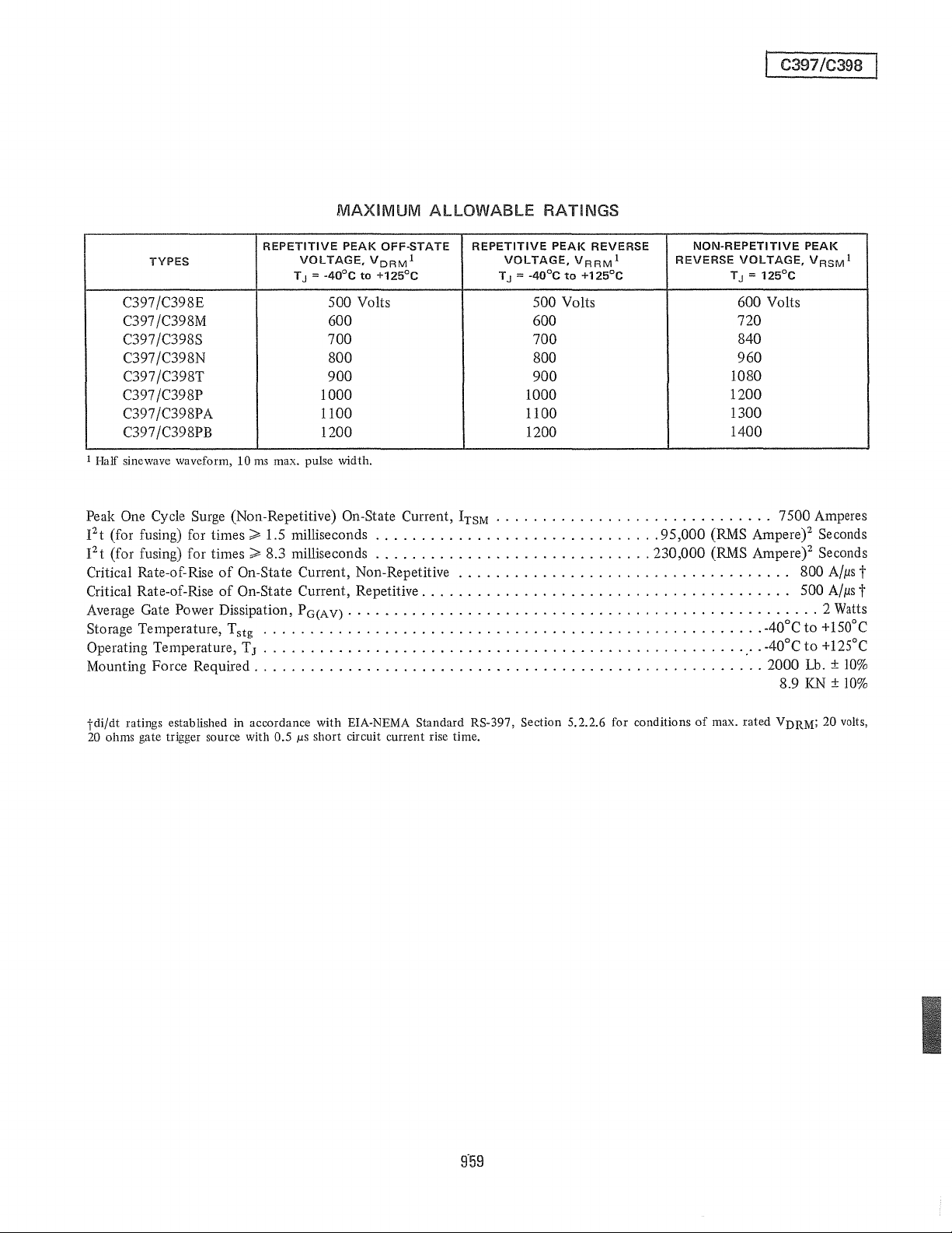
Equipment designers can use the C397/C398 SCR's in demanding applications, such as:
'"
Choppers
..
Inverters
..
Regulated Power Supplies
FOR SINEWAVE OPERATION
Uke
the
Type C140/141, C158/159 and C358 SCR's,
the C397/C398 SCR
..
Peak Current
..
Pulse Width
..
Frequency
..
Case
is
rated for:
vs.
Temperature
'"
Sonar Transmitters
'"
Induction Heaters
..
Radio Transmitters
958
..
Cycloconverters
..
DC
to
DC
Converters
..
High Frequency Lighting
FOR RECTANGULAR WAVE OPERATION
GE
now introduces a new, high-frequency rating for
the
C397/398 SCR, which is:
..
Peak Current
vs.
" di/dt
..
..
..
of
Leading Edge
Frequency
Duty Cycle
Case
Temperature
Page 2
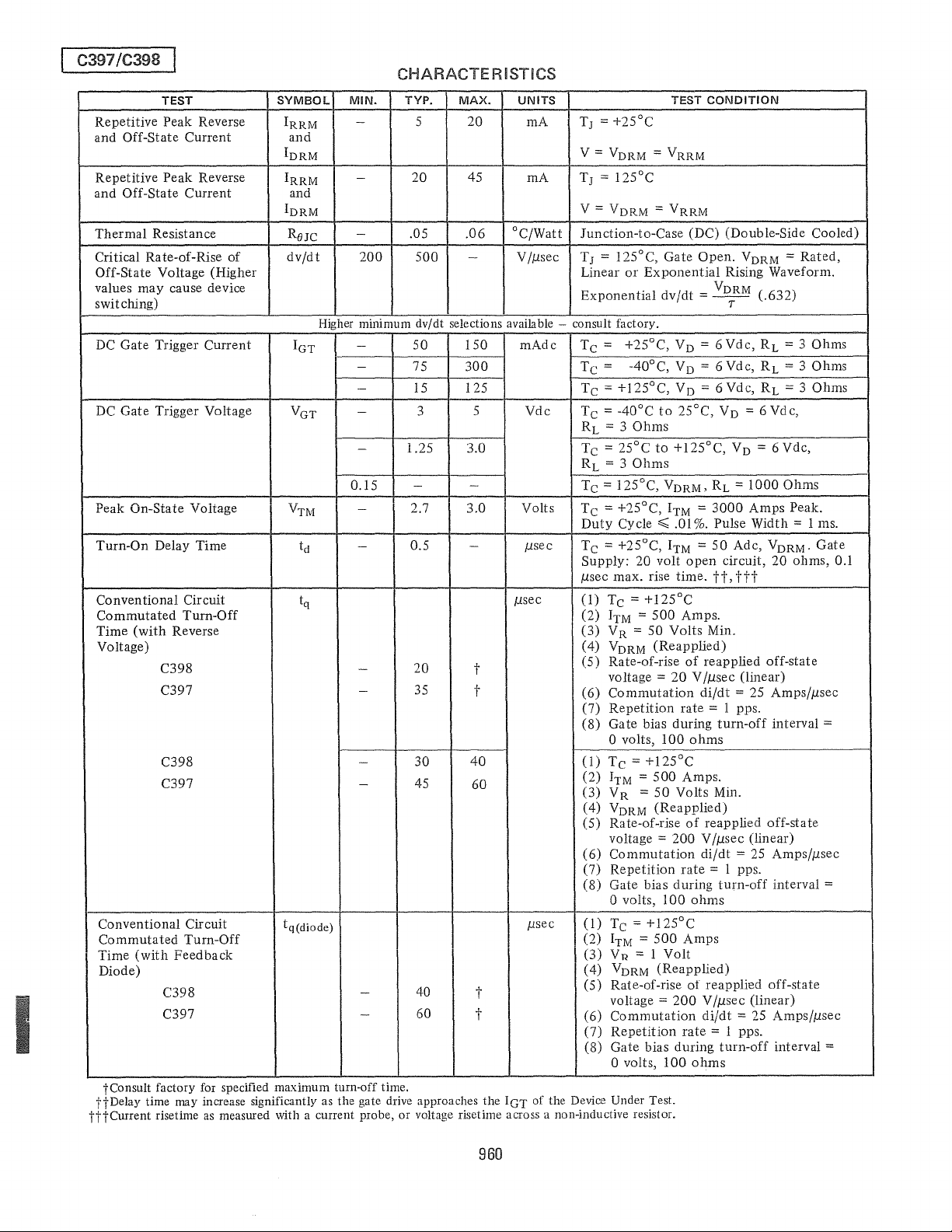
C397/C398
TYPES
C397/C39SE
C397/C39SM
C397/C39SS
C397/C39SN
C397/C39ST
C397/C39SP
C397/C39SPA
REPETITIVE
VOLTAGE,VDRMI
T
=
·40oC
J
1000 1000
1100
MAXIMUM
PEAK
OFF·STATE
to
+125°C
500 Volts 500 Volts
600 600 720
700 700
SOO
900 900
ALLOWABLE
REPETITIVE
C397/C39SPB 1200 1200
1 Half sinewave waveform, 10
Peak One Cycle Surge (Non·Repetitive) On·State Current, I
2
1
t (for fusing) for times;;;' 1.5 milliseconds
2
1
t (for fusing) for
Critical
Rate·of·Rise
Critical Rate·of·Rise
Average Gate Power Dissipation,
Storage Temperature, T
Operating Temperature, T
Mounting Force Required
ms
max. pulse width.
TSM
...............................
times;;;' S.3 milliseconds
of
On·State Current, Non·Repetitive
of
On·State Current, Repetitive. . . . . . . . . . . . . . . . . . . . . . . . . . . . . . . . . . . . . .
PG(AV)
.....................................................
stg
..•.•...•..••••..•.•.•...•..•.•.••...•......•......
J
..............................
....................................
...................................................
.......................................................
RATINGS
PEAK
VOLTAGE,
T J =
·40oC
SOO
1100
.........•....••...•..•....•..
VRRMI
to
+125°C
REVERSE
NON·REPETITIVE
REVERSE
VOLTAGE,
T
=
J
125°C
PEAK
V
RSM
1
600 Volts
840
960
10
SO
1200
1300
1400
7500 Amperes
95,000 (RMS Ampere)2 Seconds
230,000 (RMS Ampere)2 Seconds
SOO
A/ps
..
500
A/ps
2
Watts
'.'
°
.
AO
• AO°C
2000
8.9
Cto
to
Lb.
KN
°c
+150
+12SoC
±
10%
±
10%
t
t
tdi/dt
ratings established in accordance
20
ohms gate trigger source with 0.5
with
IlS
EIA·NEMA Standard RS·397, Section 5.2.2.6 for conditions
short circuit current rise time.
of
max. rated VDRM; 20 volts,
Page 3
C397/C398
CHARACTERISTICS
TEST
Repetitive Peak Reverse
and Off-State Current
Repetitive
and Off-State
Thermal
Critical Rate-of-Rise
Off-State Voltage (Higher
values
swit ching) T
DC
DC
Peak On-State Voltage V
Turn-On
Conventional
Commutated
Time
Voltage)
Peak
Reverse
Current
Resistance
of
may
cause device
Gate Trigger
Gate Trigger Voltage V
Delay Time
(with
Current
Circuit
Turn-Off
Reverse
C398
C397
SYMBOL
IRRM
and
IORM
IRRM
and
IORM
ROJe
dv/dt
IGT
GT
TM
td
tq
MIN.
-
-
- .05
Higher
-
-
-
-
-
0.15
-
-
TYP.
200
minimum dv/dt selections available - consult factory.
1.25 3.0
2.7 3.0 Volts
0.5
MAX.
5
20
500
50 150
75
15 125
3 5
-
20
45
.06
300
-
-
UNITS
rnA
rnA
DC/Watt
V
/psec
mAdc
Vdc
psec
/lsec
20
-
35
t
t (6)
TEST
=
+25°C
T
J
V = V
=
T
J
V = V
Junction-to-Case (DC) (Double-Side Cooled)
T
= 125°C, Gate
J
Linear
Exponential
Te
=
Te
=
Te = +125°C,
Tc = -40°C
RL
= 3
Tc = 25°C
RL = 3
Te
= 125°C,
Tc = +25°C,
Duty
Te
= +25°C,
Supply: 20 volt
psec
(1)
(2)
(3)
(4)
(5) Rate-of-rise
(7)
(8)
= V
ORM
125°C
ORM
or
+25°C,
-40°C,
Cycle ~ .01
max. rise
Te = +125°C
ITM = 500
V
R
VORM
voltage
Commutation
Repetition
Gate
RRM
=
VRRM
Exponential
dv/dt = VORM
Vo
Vo
Vo = 6Vdc,
to
25°C,
Ohms
to
+125°C,
Ohms
VORM,
ITM = 3000
ITM = 50
time.
Amps.
= 50
Volts
(Reapplied)
=
20 V /psec
rate = I pps.
bias during
open
of
o volts, 100
C398
C397
30
- 45
40
60
(1)
Te = +125°C
(2)
ITM = 500
(3)
(4)
(5) Rate-of-rise
(6)
(7)
(8)
=
50
VR
VORM
(Reapplied)
voltage
Commutation
Repetition
Gate bias during
=
Amps.
Volts Min.
of
200 V /psec
rate
o volts, 100
Conventional
Commutated
Time
(with
Diode)
tConsult factory
ttDelay time
tttCurrent
risetime
Circuit
Turn-Off
Feedback
C398
C397
for
may
specified maximum turn-off time.
increase significantly
as
measured
tq(diode)
as
\vith
the gate
a current probe, or
- 40
60
drive
approaches the IGT of the
voltage
psec
.1.
I
t
risetime across a non-inductive resistor.
(1)
Tc = +125°C
(2)
ITM = 500
(3)
V
= I
Volt
R
V
ORM
(Reapplied)
200
100
( 4)
(5)
Rate-of-rise
voltage =
(6)
Commutation
(7)
Repetition
(8) Gate bias during
o volts,
Device
Under Test.
Amps
ot
rate
CONDITION
Open.
V
=
ORM
Rising Waveform.
= 6
Vdc,
Rated,
(.632)
RL = 3 Ohms
= 6 Vdc, RL = 3 Ohms
RL = 3 Ohms
Vo
= 6 Vdc,
Vo = 6Vdc,
RL =
1000
Ohms
Amps
VORM.
20
Amps/psec
interval =
(linear)
Amps/psec
Peale
ohms, 0.1
%.
Pulse Width = I ms.
Adc,
circuit,
ti",
ttt
Min.
reapplied off-state
(linear)
di/dt
= 25
turn-off
ohms
reapplied off-state
di/dt
= 25
= I pps.
turn-off
ohms
reapplied off-state
V/psec
di/dt
(linear)
= 25
interval =
Amps/psec
= 1 pps.
turn-off
ohms
interval =
Gate
960
Page 4

SINE WAVE
CURRENT
RATING
DATA
C397/C398
10,00 0
1000
I-----
"""",r:::::
-
-
~-.
1---
1.
MAXIMUM
CURRENT
s,,-s
?\l\.- -
.-
'--
.
lor
1+
+~i()~~-
?"-~
-'
500D,INV
SOOO
sooo
100 1000
ALLOWABLE
VS. PULSE
<f)
iii
l\'
:Ii
<!
1
,...
Z
W
0::
0::
::0
U
Cl
0::
3!
f5
"-
'"
"
l\'
c-
<~,
2S00
PARALLEL
PULSE BASE WIDTH
--
- - 2011,
SNUBBER
1000
1000
DIODE
(,...SEC)
PEAK
WIDTH
511,.2"f
--
'400
--5n,.2~f
--20n
_.-
2"f
CIRCUIT
1
1"--"
..
ZJ.lf
20n,.2}1f
WITH INVERSE
PARALLEL
ON-STATE
(Tc
= 65°C)
,I
DIODE
10iJQO
r----
1---1
60
1000
~-,
....-:
--
101(
2.
I
s,,-s
?\l\.-
v
.......
-
,~
1-1--
!-I--
-
.-
1°'1
MAXIMUM
CURRENT
I I
I
s,,-CO""/-
?~?-
r---
-
--
~1500
100
PULSE
ALLOWABLE
VS. PULSE
\)
2500
BASE
--
WIDTH
1
I
~
1000
1000
(J.'SEC)
PEAK
WIDTH
,"-
400
--50
•.
-
-200,.2,..'
ON-STATE
(Tc
I'---,
60
2/--,'
10K
= 90°C)
3.
ENERGY
NOTES:
(Pertaining
1.
2. Reverse voltage
3.
4.
5.
6. Double-Side Cooled.
7. Values of W-S/P
PER
to
Sine
Switching voltage ~ 800
Max. energy
total
W-S/P
of
for
operation
Required
20
volts,
amps/J.l.sec
20
volts, 20
100
amps/J.l.sec.
RC
Snubber
PULSE BASE WIDTH
PULSE FOR
and
Rectangular
applied
dissipated
shown
with
gate drive:
65
inverse
ohms, 1 J.l.sec
ohms, 5 J.l.sec
ckt. = .2
are
("SEC)
SINUSOIDAL
or
Wave
Current
volts.
= VR
~
800
dur ing reverse recovery
or
0.03
diode.
risetime
risetime for
J.l.f,
5!'t
for
TJ = 125°C.
V.
W-S/P whichever
for
961
PULSES
less
than
greater
Ratings)
is
15%
is
least
100
than
Page 5

C397/C398
RECTANGULAR
WAVE
CURRENT
RATING
DATA
U)
w
0::
w
"-
:;
'?
f-
Z
w
0::
0::
::;J
u
w
t:r
f-
U)
z
0
,
'"
w
'"
"-
1000
900
SOO
700
600
500
400
300
200
100
-
-
-
-
t-!:,.ULSES
4.
MAXIMUM
DUTY
CYCLE
---e-.
r--
---
PER
SECOND
I
10
RATE
OF
RISE
OF
ON-STATE
ALLOWABLE
CURRENT
VS
- 50%
di/dt
--
CURRENT
PEAK
(Tc
"-
-IA/!-,SECI
ON-STATE
= 65°C)
100
60
400
1000
2500
5000
DUTY
~
'
........
1000
UJ
w
900
0::
W
-
-
-
"-
:l;
<l
I
fZ
w
0::
0::
::;J
u
w
~
'?
z
0
<l
'"
W
"'-
800
700
600
500
400
300
200
100
-
,
6.
MAXIMUM
r---
......
~
F>(;
......
L..s
'8~
10
RATE
CURRENT
CYCLE -
I'--
-..
-
-..
i'--
COrvD
OF
RISE
OF
ON-STATE CURRENT
ALLOWABLE
VS.
25%
-
-
-
-
-
-
PEAK ON-STATE
di/dt
(Tc
= 65°C)
-
-IA/!-,SECI
100
60
400
1000
2500
5000
-
U)
w
0::
w
"-
:l;
I
'"
f-
Z
w
0::
0::
::;J
u
w
~
'?
z
0
'"
w
'"
"-
1000
900
800
700
600
500
400
300
200
100
I---
::rP~
I I
r'"
....
5.
MAXIMUM
SES
PER
SECOND
..
r---..
10
RATE
OF
ALLOWABLE
CURRENT
I--
-
2500
~
RISE
OF
ON-STATE CURRENT-IAI!-'SECI
VS.
di/dt
I'-
--
PEAK
(Tc
= 90°C)
60
400
1000
-
100
ON-STATE
NOTES: (SEE
UJ
w
1000
0::
W
900
"-
::!'
800
700
I
'"
f-
Z
600
w
0::
0::
500
::J
U
-
SINE
w
~
'?
z
0
'"
w
'"
"'-
WAVE
400
300
200
100
DATA)
-
__
-
7.
-
PULSES
P
~~
10
RATE
MAXIMUM
CURRENT
r--
-
OF
RISE
OF
ON-STl\TE CURREI'.IT-(A/p.SEC)
ALLOWABLE
VS.
I"'--
l-
di/dt
-
-
I'-
t-
PEAK
(Tc
i-I-
1-1-
:-
= 90°C)
60
400
1000
I-!-
2500
100
ON-STATE
-
962
Page 6

(/)
Ii!
w
a..
:!:
<t
~
1000
Z
~W4rr_
w
a::
a::
:::>
u
w
~
(/)
I
Z
0
<t
'"
W
a..
100
10
100
10
-
t--
r--
r---s~cOND
r--
r--...
--
~
I--
r-..
P~F/
"
r-...
1-1--
r--.
r-.
1--
I"-
........
~
~
.........
.........
2.:;
~
l'-
PULs~
r--...
./
---.........
t---
100 1000
PULSE
BASE
'I"-
~
i""'-
l'
1'--
i'-
I'l'
1'-
1'-
l'
WIDTH-("SEC)
"-
tr41'
..........
"-
i"'-..
i<.........
100
"-~
1'~8
~CO
~"'~
--...,
~S
"
f'.....
PULSE
BASE
'''"
~'"
U(8~
~'
I"-
I'-
'"
1'--
1'-
l'
WIDTH
("SEC)
'r--
WATT-SECOND
~
'~s
I
'"
""'-
""
~
r~
.....
r--
~
I
~
""
"'"
1'""
,
'"
""
~
~
1000
~
"'"
"
~
PER PULSE
~-
~
""
"'-
i'-.
s
,
~
"-
f-
i'
f'.
l"-
I"-
Kh'-
I"!,-
l'f',
10_1-
l'-
l'
!'-
!'-1"-
f',
C397/C398
R
ENERGY
AND
t-
10K
9.
ENERGY
AND
10K
PER
PULSE VS,
PU
LSE
WIDTH
PER PULSE VS.
PULSE
WIDTH
PEAK
(di!dt
= 100 A!/lsec)
PEAK
(di/dt
CURRENT
CURRENT
= 25 A!/lsec)
(f)
l!i
w
a.
~
I
...
ili
0:
0:
a
~
(f)
'"
I
Z
0
~
a.
1000
100
tr41'~
'~8
~~co
KD
I~
100
l'
t'--['
"'1'
~
,
--...,
--...,
,
"'~
0'",
~U(8~
",
"~s
i'-
"I'
PULSE BASE
WIDTH
~/O
~
!-.....I
·s
I~
~
1000
-i"SEC)
I'-.s
<.s
"
'"
"-
~
~
"
,
'"
'"
1'-.
r"
'"
"I'
963
!'-
f',
10K
10.
ENERGY
AND
NOTES: (SEE SINE
PER PULSE VS.
PULSE
WIDTH
PEAK
(di!dt
WAVE
CURRENT
= 5 A!psec)
DATA)
Page 7

C397/C398
Ul
w
a:
w
"-
:::
«
,
I-
2
W
a:
a:
::J
U 1000
w
l-
i:':
Ul
;2
o
Ul
::J
o
W
2
i:':
2
i:':
Ul
'?;
11.
./
./
/ I
L L
J I
/
I
INSTANTANEOUS
MAXIMUM
~
25
0
V'i25°c
---
V
~
i
2 3
ON-STATE
ON-STATE CHARACTERiSTICS
VOLTAGE-VOLTS
300,000
250,000
u
W
Ul
200,000
N
-0::
150,000
"!~
Ul
::l:
a:
100,000
80,000
15,000
10,000
8,000
6,000
4
5,000
1
14. SUB-CYCLE SURGE (NON-REPETITIVE)
ON-STATE
V
".....
INITIAL
TJ =
t--
1.5
2 4 6
PULSE 8ASE
CURRENT AND
.......
-40°C
WIDTH
.........
TO
+125°C
(mSEC)
J2
t
.....
...-
RATING
-
8
10
Ul
':i
o
>
,
w
---
'"
~
10
o
>
W
I-
«
'"
Ul
::J
o
W
2
i:':
2
;:!
Ul
?:
8,000
U;
7,000
w
0:
WW
d
~«
~76,000
-I-
Ul2
W
lLa:
...Ja:
~a
><w
~!;i5,OOO
"-I-
Ul
2
o
13. SURGE (NON-REPETITIVE) ON-STATE CURRENT
/'
./
/
lL
rTF
~
~J/
I
.1
12. GATE TRIGGER CHARACTERISTICS
~
<
~
"
./,"40°C
C
2
r
!'"
,/"
INSTANTANEOUS
""'"
~
~
"'-
INljlALI
TJ
2 4 6 8
1\
,-
."
"
~
~"
."~-<"o
o
i-"'f'"
GATE
POWER
'~
1=
l-rill
CYCLES
~
"
~~,.+
"'.
~O'
6'
It--.
~Id
1;.05'
;q}-}-
4?
;q}-.-
05'<"0
}-U'-I-~
1?:}
~"-
"-
.........
",
/20V,2i.\l
CURRENT-(AMPERES)
RATINGS
~"
10
AT
-
r-....
0
O
C
+125
1
60
Hz
'l
0
05'
1?;q
0
-'<&
20
_4?;q
r-
V
l"-
~
1-"
~o
.....
.....
i'
/0
05'
~
"-
~
f~
AND
r--
40
~
05'
01?
"7+:--
...
60
If-
.
80100
10
NOTES:
1.
2.
964
The
locus
boundaries
20V rate of circuit
of
}.LS
Maximum
amps/}.Ls
iii
!Xl
::E
0
...J
::J
0
u
3-
,
?
"-I
a:
'"
«
J:
u
0
W
a:
W
>
0
u
W
0:
of
shown
20
is
current
max. rise time.)
G
w
0:
~
rise>
long
with
100
10
15.
possible
the
de
trigger
at
various case temperatures.
minimum
current
200
term
20V -20n
TYPICAL
gate source load line
rise> 1 00
amps/}.Ls
repetitive
gate source.
RECOVERED .CHARGE (125°C)
SINEWAVE
points
lies
outside
the
amp//-Ls
(Tp = 5
anode
REVERSE
CURRENT WAVEFORM
when
or
anode
}.LS
min.,
di/dt = 500
lOa
di/dt
-(AI!-,S)
rate
0.5
1000
Page 8

3
"-
o
o
W
~
;30
W
!l.
;;;
..J
«
::;:
a:
w
I
l-
I-
t;]
iii
z
«
a:
I-
.00
.0001
.0001
[ C397/C398
.1
vI--"
I
V
V
/
I
.001
16.
TRANSIENT
.01
TIME -
SECONDS
THERMAL
JUNCTION-TO-CASE
IMPEDANCE -
DOUBLE SIDE COOLING
10
~~
CA~M~'~~GE
ii,
\1.
T =
LENGTH
OF
STRAIGHT
LEAD
I<>---
OUTLINE
H *
K
~1
I
..
-..l
k-ipT;~!i']i,.1
Q
TYP.
~
R
r!
DRAWING
1
SYM
MIN.
A
B
C
0
E
F
G
H
J
K
L
M
N
p
Q
R
S
T
12.200 12.360
U
DECIMAL
INCHES
MAX.
.240
.186
.060
2.200 2.500
.030 .130
1.000 1.065
.030
.no
1.300
.110
.245
.011
.056
.067
.137
.260
.130
.191
.075
1.430
1.065
.019
.060
.096
.150
1.345
2.150
.083
.153
METRIC
M.M.
MIN.
6.096
2.794
6.223
4.724
1.524
55.88
2.794
.762
1.422 1.524
25.40
.762
3.302
33.02
1.70
309.9
313.9
3.480
MAX.
6.604
3.302
4.851
1.905
36.32
27.051
63.50
3.483
3.302
27.05
2.438
3.810
34.16
54.61
2.11
3.886
965
 Loading...