

Page 1
600
Volts
(500-700)
Amps
le393
95
RMS
The General Electric C392, C393,
for
fiers are designed
power
C394
switching
diffused Press-Pak devices employing
FEATURES:
" Fully characterized for operation in inverter and
" High
..
" Rugged
IMPORTANT:
High
di/dt
ratings.
dv
/dt
capability
hermetic
Mounting instructions
1300
"00
;;;
:t
1000
~
;]
~
~
~
~
~
glazed ceramic package having 1" creepage path.
0
--1-+-+++-1-1- \
1-
900
-
600
700
600
f\J'L
500
SINUSOIDAL
'00
300
200
WtNEFORM I I
50%
DUTY
180°
CONDUCTION
65°C
CASE
600
VOLT
5n,o.2}JF
oL-~~~~~lll_-L-L~~llL_~
with
selections available.
on
the last page
HIGH
'"
-I-
~
\ I
1\
CYCLE
TEMPERATURE
SWITCHING
SNUBBER
FREQUENCY
IN
Hl
FREQUE
-I-~I-H--I--I
"".
++--1--1
CJ95
1
1
H-t-N+--i--I
-----1-
10,000
and C395 Silicon
at
high frequencies. These are
the
field-proven amplifying gate.
chopper
of
specification
I
1
Controlled
applications.
must
be followed.
1000
m
~
900
:]"
BOO
-TI
I
~
700
~
:::
~M
~
50%
~
400
1800
~
300
65°C
~
600
i
200-
5 n
~
100
rttH--
-i------ri--I--I~~H-+
Recti-
a11-
NGS
I
-----1---1---1---1-1\
~
DUTY
CYCLE
CONDUCTION
CASE
TEMPERATURE
VOLT
SWITCHING
,0.!2}JF
100
-I
SNUB
1 I
AMPLIFYING
I----Ig~~'t__I-I-+++H
GATE~t
L,I\-''----+_~-_-L
~
--
-----j---i-++++H
--'\.------+----I--++-+-+-H
BE
R
T+i
FREQUENCY
~
------I-~--~---I-W-
il--+---I--H-+H+I
1000
IN
Hz
10,000
Equipment
" Choppers
..
Inverters
Like the
Type
designers can use the C392, C393, C394,
" Regulated Power Supplies
..
Cycloconverters
FOR
SINEWAVE
C140/141,
OPERATION
C158/159
and C358 SCR's,
the C392, C393, C394, C395 SCR's are rated for:
..
Peak Current
vs.
..
Pulse Wiclth
..
Frequency
..
Case
Temperature
C3
947
5 SCR's
in
demanding applications, such as:
"
DC
to
DC
High Frequency Lighting
"
FOR
RECTANGULAR
WAVE
Converters
OPERATiON
G E now introduces a new, high-frequency rating for
the
C392, C393, C394, C395 SCR's, which are:
..
Peak Current
vs_.
..
di/clt
of
Leading Edge
" Frequency
Duty
Cycle
" Case
Temperature
Page 2
I C392/C393/C394/C39S1
MAXIMUM
ALLOWABLE RATINGS
Repetitive Peak
TYPES
C392,C393,C394,C395A
C392,C393,C394,C395B
C392,C393,C394,C395C
C392,C393,C394,C395D
C392,C393,C394,C395E
C392,C393,C394,C395M
o Half
sinewave
Peak One Cycle Surge (Non-Repetitive) On-State Current, I
Peak One Cycle Surge (Non-Repetitive) On-State Current, I
2
1
t
(for
2
1
2
1
2
1
Critical Rate-of-Rise
Critical Rate-of-Rise
Average Gate
Storage
Operating
Mounting
fusing) for times;:;' 1.5 milliseconds - C392, C393 . . . . . . . . . . . . . . . . . .
t
(for
fusing) for times;:;' 1.5 milliseconds - C394, C395
t
(for
fusing) for
t
(for
fusing) for times;:;' 8.3 milliseconds - C394, C395
Temperature,
Temperature,
Force
waveform,
Oower
Required
10
times;:;'
of
On-State Current, Non-Repetitive . . . . . . . . . . . . . . . . . . . . . . . . . . . . . . . . . .
of
On-State Current,
Dissipation, P
Tstg
......................................................
T
.•......................•.......•................•....
J
.......................................................
Off-State Voltage,
T
=
J
ms
max.
pulse
8.3 milliseconds - C392, C393
G(A
V)
CD
V
ORM
-40°C
to
+125°C
100 Volts
200
300
400
500
600
width.
Repetitive.
....•............•...•...............•..•.........
. . . . . . . . . . . . . . . . . . . . . . . . . . . . . . . . . . . . .
Repetitive Peak
Reverse Voltage,
VRRMCD
T
= -40°C to +125°C
J
200
300
400
500
600
(60
(60
Hz)
Hz)
TsM
TSM
....................
....................
....................
100
Volts
- C392, C393
- C394, C395
.............
.............
..
50,000
100,000
120,000
250,000
Non-repetitive
Reverse Voitage,
V
T
150
300
400
500
600
720
(RMS
(RMS Ampere)2 Seconds
(RMS Ampere)2 Seconds
(RMS Ampere)2 Seconds
RSM'D
= 125°C
J
Volts
Ampere?
Peak
5500
8000
..
..
_40°C
_40°C
2000
8.9
800
500
Amperes
Amperes
Seconds
Alps t
Alps t
2 Watts
to
+150°C
to
+125°C
Lb. ±
KN
±
10%
10%
I
tdi/dt ratings established in accordance with
20
ohms
gate trigger source with
TEST
Repetitive Peak Reverse
and Off-State
Repetitive Peak Reverse
and
Off-State
Thermal Resistance
Critical Rate-of-Rise
Forward
(Higher values may cause
device switching)
Holding Current
DC
Gate Trigger
Current
Current
Blocking Voltage
Current
of
0.5
}J.S
short trigger current
SYMBOL
IRRM
and
IORM
IRRM
and
IORM
ROJe
dv/dt
Higher
IH
IGT
EIA-NEMA
Standard
rise
time.
CHARACTE R ISTiCS
MIN.
-
-
200
-
-
-
TYP.
S
20
.OS
SOO
minimum dv/dt selections
40
70
100
2S
RS-397,
MAX.
.06
1000
200
400
ISO
Section 5.2.2.6 for conditions of
UNITS
IS mA
4S
DC/Watt
-
V/psec
available
mAdc
mAdc
mA
max.
rated
VDRM;
TEST
CONDITION
T
= +2SoC
J
V =
VORM = VRRM
TJ
= 12SoC
V =
VORM
Junction-to-Case (Double-Side Cooled
TJ =
Linear
Exponential
consult factory.
Te
= +2SoC, Anode Supply =
Initial On-State Current = 10 Amps.
Te
=
Te
=
Te
= +12SoC,
= V
+l2SoC,
or
Exponential
+2SoC,
-40°C,
RRM
Gate
Open. V
Rising Waveform.
dv/dt = VO_RM
"'
Vo
= 10 Vdc,
Vo
= 10 Vdc, RL = 1
Vo
= 10 Vdc, RL = 1
ORM
(.632)
24
RL
= Rated
Vdc,
= 1
20
Ohm
Ohm
Ohm
volts,
948
Page 3
TEST
DC
Gate
Trigger Voltage V
Peak On-State Voltage
C392, C393 3.3 4.2
C394, C395 2.3 2.5
Turn-On Delay Time
Conventional Circuit
Commutated
(with
Time
Turn-Off
Reverse
Voltage)
C392,
C394
C393, C395
C392,
C394
C393, C395
Conventional Circuit
Commutated
Time
(with
Turn-Off
Feedback
Diode)
C392, C394
C393, C395
tConsult
HDelay
tHCurrent
factory for specified maximum turn-off time.
time may increase significantly as the gate drive approaches the IGT
risetime
as
SYMBOL
GT
MIN.
-
-
0.15
VTM
td
-
tq
-
- 12
-
-
tq(diode)
-
measured with a current probe,
CHARACTERISTICS
TYP.
3
1.50
0.5
8
MAX.
3.0
-
-
UNITS
5
Vdc
Tc = _40DC
RL
= 1
Tc
= 25
RL = 1
Tc
= +125
Tc
Volts
= +25
Duty
Cycle ~ .01%.
Pulse Width = 3.0 ms
Tc
/lsec
= +25
Supply:
/lsec max. rise time.
0.1
(1)
/lsec
t
t
Tc
(2)
ITM
(3)
V
R
(4)
VORM
(5) Rate-of-rise
voltage
(6)
Commutation
(7)
Repetition
(8) Gate bias during
o volts, 100
12
17
14
20
(1)
Tc = +l25
(2)
ITM
(3) V
R
(4)
VORM
(5) Rate-of-rise
voltage
Commutation
(6)
(7) Repetition
(8) Gate bias during
o volts, 100
(1)
Tc = +l25DC
(2)
ITM
(3)
VR
(4)
VORM
(5)
Rate-of-rise
voltage
(6)
Commutation
(7)
Repetition
(8) Gate bias during
18
25
/lsec
t
t
o volts, 100
of
or
voltage risetime across a non-inductive resistor.
the Device Under Test.
I C392/C393/C394/C395!
TEST
CONDITION
to
25DC,
Vo
Ohm
D
C
to
+125DC,
Ohm
D
C,
VORM,
D
C,
ITM = 3000
D
C,
ITM
20 Volt
D
= +125
= 50 Volts Min.
C
= 500 Amps.
(Reapplied)
= 20 V //lsec (linear).
rate = 1 pps.
D
= 500 Amps
= 50 Volts Min.
(Reapplied)
= 200 V//lsec (linear).
rate
= 500 Amps
= 1 Volt
(Reapplied)
=
200
rate = 1 pps.
Vo = 10Vdc,
RL =
= 50 Adc,
Open
Circuit,
of
reapplied off-state
di/dt = 25
turn-off
ohms
C
of
reapplied off-state
di/dt
= 1 pps.
turn-off
ohms
of
reapplied off-state
V//lsec (linear).
di/dt
turn-off
ohms
= 10 Vdc,
500
Ohms
Amps
Peak
tt,
VORM.
ttt
20
Gate
Ohms,
Amps//lsec
interval =
= 25 Amps//lsec
interval =
= 25 Amps//lsec
interval =
10,000
1000
100
~
/
1-
f--
I-
t--
r-TTIII
10
f---
1-15,000
IO,DOOHl.
4
,1
PULSE
l--
1""00
100
I-
2500
"
BASE
1'>(;
l..SF~
r--
I'-
1'1000
"
WIDTH-(jLSEC)
1000
1
"'Z1'>~1r
~co
1\10
~60
10K
"400
I
n.
949
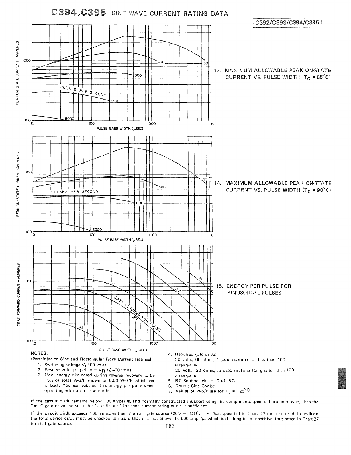
3.
MAXIMUM
CURRENT
SINE WAVE CURR
ALLOWABLE PEAK ON-STATE
VS.
PULSE WIDTH
RATING
(Tc
= 65
D
DATA
Cl
Page 4
I
C392/C393/C394/C39S!
r--t--- I
100.L-
__
10
I-i~,o~o
-L
__
L-~-ULU~
10,000
I I I
IV,
I
100
PULSE
__
-L
BASE
__
L-~-LLLU-
WIDTH
4.
MAXIMUM
CURRENT
__ ~ __
1000
-(
fL
SEC)
~~LL~U
101<
ALLOWABLE
VS. PULSE
PEAl< ON-STATE
WIDTH
(Tc
= 90°C)
Ui
w
n:
w
n.
O!
"
IW
I-
oW
2:
n:
n:
::J
u
w
<t
l-
f
z
c
<t
"
n.
10,000
1000
100
-
!--
---
10
-
-1-1-
-
--
---
I'---......
.........
.........
r£Z
t"'--
~
h
"'~
~
.........
l'.........
"
~
I'
100
PULSE
BASE
I,
"-...
/Y-<J1'
I'-.
~~8
~co
~~,
"'-
"
...............
~O
~
WIDTH-(fL
~
~
,o~-)l
~
i'
,0&
<8:--
-...
...
f-
'~
N's
...............
"
O"S
l'...
'"
~
1000
SEC).
~
~S
'"
'r.........
r.........
i'-..
"'~
!i'-..S
.........
'"
'"
'"
5.
ENERGY
SINUSOIDAL
PER
PULSE FOR
PULSES
"-
10K
950
Page 5
95
I C392/C393/C394/C395 I
If)
w
a:
w
Q.
;;;
,
"
I-
Z
w
a:
a:
::0
u
w
~
'{'
z
0
'"
W
"
Q.
1000
900
800
700
600
500
400
300
200
100
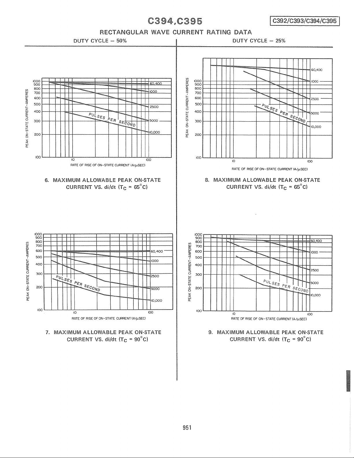
6.
MAXIMUM
RECTANGULAR
DUTY
CYCLE - 50%
--
--
~L.SF::S
10
RATE
OF
CURREr~T
----
r---
-
PF::f/
r--~COND
RISE
OF ON-STATE CURRENT (A/f'-SEC)
ALLOWABLE
VS.
di/dt
r-
-
r-~_
1'-_
PEAK
ON-STATE
(TC
= 65°C)
I'
1',..
WAVE
40r
1000
2500
5000-
10,000
100
CURRENT
U1
w
1000
a:
900
w
0..
800
;;;
700
,
"
I-
600
z
w
a:
500
a:
::0
u
400
w
l-
i'!
'{'
300
z
0
'"
w
200
"
0..
100
RATING
8.
MAXIMUM
DATA
DUTY
...............
10
RATE
OF
RISE OF
ALLOWABLE
CURREl"JT
CYCLE - 25%
-
...........
......
............
~S"S
ON-STATE
VS. di/dt (Tc = 65°C)
r-
--
......
-
--
......
r--.
.......
1"--.,
.....
r--.
•· • .""IT
1'~"cONo
CURRENT (A/f'-SEC)
PEAK
ON-STATE
i""-
60,400
1000-
2500-
5000-
10,000
100
If)
w
a:
w
u.
;;;
'i'
I-
Z
w
a:
0::
::0
U
w
~
'{'
z
0
'"
W
"
u.
1000
900
800
700
600
500
400
300
200
100
±t±
-
.......
i...!lJL.SF::
7.
MAXIMUM
r--
i""-
~
r--.1'i""-~P"Fi'
r---
--"""'1'-
S"
CONO
I--
-
rr-
-
-
r--
10
RATE
OF
RISE
OF
ON-STATE CURRENT (A/f'-SEC)
ALLOWABLE
CURRENT
VS.
di/dt
PEAK
(Te
ON-STATE
= 90°C)
60,400-
1000
2500
5000
10,000
100
U1
w
a:
w
u.
;;;
,
"
I-
Z
w
a:
a:
::0
u
w
~
'{'
z
0
'"
w
"
u.
1000
900
800
700
600
500
400
300
200
100
9.
MAXIMUM
......
.............
...
...............
...............
10
RATE
OF
RISE
ALLOWABLE
CURRENT
I--.
-
-.......
-
...............
--
~L.SF::S
OF
ON-
STATE CURRENT (A/f'-SEC)
VS.
di/dt
-
r-
-
--
PF::f/
--r-SF::COND
-
r-
PEAK
ON-STATE
(Te = 90°C)
60400
1000-
2500
5000
~
10,000
100
I
951
Page 6
I C392/C393/C394/C39S1
IOPOO
I'r-
Jv-1I'~'i'---""
"-
-.........
""
.......
""
~
~"'i
100
PULSE
1000
10p0Q
100
10
...............
i"---..
~
"I'
~~
1','.5'-~
'::-0
°l\t
o
""A.::-
,,-»
A
u<
""
"
BASE
f'..-
WIDTH-(,u
&.::-l~s
"i--:
r'J
ml\
"'"
1000
SEC)
C39
-SECOND
'I'
"'"
~
"
/
i'.
"
"'"
r"
""
/0
,C39
10K
PER
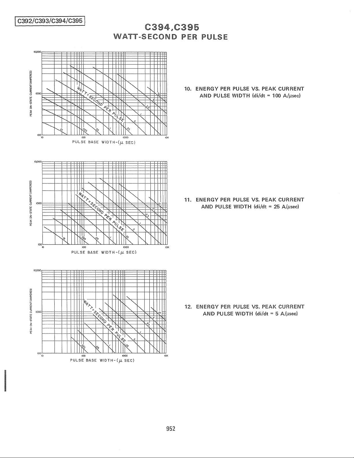
10.
PULSE
ENERGY
AND
PULSE WIDTH
PER
PULSE VS. PEAK CURRENT
(di/dt
= 100 A/jlsec)
1000
10,000
1000
100
100
I""
Kl
I---
10
""
K
""
'"
"'-1'~
1')'0
"&<,<:
Co
I'
"'"
'"
R~
100 1000
PULSE
BASE
"'-<{
)'oJ'"
t5'~
Co
"-
"-
"-
""
R""
~
100 1000
PULSE
BASE
1',
""'I'-,
~o
A~
'"
WIDTH-(IL
I"
"
i'-
'V
O
I",A~
1'-,1>
""'~
-»
Au
"
!{&~
~
~
J
lIi\
SEC)
I"
"",""
"
"<>v
",('
t5'
~
""'"
~ffi\
WIDTH-
(,u
SEC)
"'"
"-
/
"'"
~
""
/
'"
""
"-
~
"-
i'-
"
~"
i'-
s
"
-
-
PER
/0
10K
/0
10K
11. ENERGY
AND
12. ENERGY
AND
PULSE VS.
PULSE WIDTH
PER
PULSE VS.
PULSE WIDTH
PEAK
(di/dt
PEAK
(di/dt
CURRENT
= 25 A/jlsec)
CURRENT
= 5 A/jlsec)
I
952
Page 7
SINE
WAVE
CURRENT
RATING
DATA
I C392/C393/C394/C395 I
Ul
w
a:
w
a.
:;:
<I:
I
I-
Z
w
a:
a:
:::J
U
w
l-
f'!
Ul
,
Z
0
<I:
'"
w
a.
Ul
w
a:
:s:
~
I
I-
aJ
a:
a:
:::J
u
W
~
Ul
~
<I:
'"
:s:
1000
100
1000
100
i--
10
10
.......-
./'
I-
-
.7
-
I--
PULSES
1--'
......
PULSE::S
5000
V
I--'
~
PER
r-
t-t-
~
~
r-
PE::R
t-
SE::COND
-..::::..
100 1000
12500
PULSE BASE WIDTH (~C)
~
V
>-
SECOND
l-
I--
2500
100
PULSE BASE WIDTH (fLSEC)
...........
!'-'
.............
'-
~
'r--
I'-,
60
1'-,60
13.
10K
14.
10K
MAXIMUM
CURRENT
MAXIMUM
CURRENT
ALLOWABLE
VS. PULSE
ALLOWABLE
VS. PULSE
PEAK ON-STATE
WIDTH
WIDTH
PEAK
(Tc
= 65°C)
ON-STATE
(TC
= 90°C)
r-
--
400
1000
t--..
~
~400
t-
1000
1000
Ul
1\!
~
~
1000
u
I
~
w
a.
I--
--
NOTES:
(Pertaining
If
the
"soft"
If
the
the
for
to
Switching
1.
2. Reverse voltage
3. Max.
total
stiff
energy
15%
of
is
least.
operating
circuit
gate drive
circuit
device
gate
r-r-..
-
-
Iff
Sine
and
voltage ~ 400
dissipated
total
W-S/P
You
can
with
di/dt
remains
shown
di/dt
exceeds
di/dt
source.
r-.
r---
1--
1"-"
,
.............
,
-........
tv
~/'/,
~~C'O
~
i'...
100 1000
Rectangular
applied
= VR
during
shown
subtract
an
inverse
below
under
100
must
be
checked
""
Wave
~
400
reverse
0.03
energy
amps//-ls,
to
"
Current
volts.
W-S/P
per
for
then
insure
PULSE BASE WiDTH (I-LSEC)
volts.
or
this
diode.
100
"conditions"
amps//-ls
1'-
~
'"
"-
.~;O~~
Ratings)
recovery
whichever
pulse
and
each
the
that
"-,./
"-
~
l
~
,,-?
~
&~
~'
to
be
when
normallv
current
rating
stiff
gate
source
it
is
not
above
"-
"
4.
5. RC
6.
7. Values
constructed
953
"
~
I'
s
Zs
,
',,-
,
"
"
'"
Required
20
volts,
amps//-lsec.
20
volts,
amps//-lsec
Snubber
Double-Side
of
snubbers
curve
is
sufficient.
(20V
- 20.11),
the
500
amps//-ls
1'1:>
,
~
10K
gate
drive:
65
ohms, 1 /-lsec
20
ohms,
ckt.
Cooled
W-S/P
are
using
tr
= .5/-ls, specified in
which
15.
ENERGY
SINUSOIDAL
risetime
.5
/-lsec
.2
/-If,
5.11.
for
T J =
the
components
is
the
long
risetime
125°C'
term
PER
for
for
specified
Chart
repetitive
PULSE FOR
PULSES
less
than
100
greater
than
are
27
must
be used.
limit
100
employed,
noted
then
In
addition
in
Chart
the
27
Page 8

I C392/C393/C394/C395 I
RECTANGULAR
WAVE
393
g
CURRENT
RATING
DATA
(J)
w
Cl:
w
"-
:;;
<!
I
f-
Z
w
Cl:
Cl:
::>
u
w
~
'?
z
0
<!
'"
w
"-
1000
900
800
700
600
500
400
300
200
100
--
16.
MAXIMUM
DUTY
----
r-
~R
10
RATE
OF
RISE
ALLOWABLE
CURRENT VS
CYCLE -
-
r--
50%
-
r--
-
SECOND
OF ON-STATE CURI<ENT
PEAl< ON-STATE
di/dt
(Tc
= 65°C)
I"-
i'-
I-I'-i'=-
-(AI,uSEC)
100
60
400
1000
2500
DUTY
1000
900
800
(J)
w
700
Cl:
w
Il.
600
:;;
<!
-
-
I
f-
Z
w
Cl:
Cl:
::>
u
w
~
'?
z
0
<!
'"
W
Il.
500
400
300
200
100
I--
rr-
1-1'-
-Pu
......
~Sf:s
.........
18.
MAXIMUM
CURRENT
CYCLE -
---
--
----
Pf:fr
.............
.......
-
-
........
!--r-..
25%
T-h
10
RATE
OF
RISE
OF ON-STATE CURRENT
ALLOWABLE
VS.
cli/clt
-r-
I-
r""'-
--
tt
PEAl< ON-STATE
(Tc
= 65°e)
I'-i'=-
I'-i'=-
F-
r-
-(A/,uSEC)
60
400
1000
2500
100
-
(J)
w
Cl:
w
"-
:;;
<!
I
f-
Z
w
Cl:
Cl:
::>
u
w
~
f-
(J)
I
z
0
<!
'"
W
Il.
1000
900
800
700
600
500
-
::':UlS
400
300
200
-
100
17.
~v1AXlr111urv1
NOTES:
(Pertaining
1.
RC
2.
Off-State
3. Reverse voltage
4.
Maximum
5. Max.
15%
is
operating
ES
PER SECOND
10
RATE OF
AllOVVABlE
CURREi\IT VS.
to
Sine
and
Snubber
least.
ckt.
Voltage = 400
TJ = +125°C.
energy
of
total
You
with
dissipated
W-SYP
can
RISE
OF ON-STATE CURRENT
di/dt
Rectangular
=
.25J.Lf,
5n·
volts.
=
50V
';:;;VR ';:;;400
during
shown
subtract
an
inverse
diode.
-(A/,uSEC)
PEAK Oi\i-STATE
(T C = 90°C)
Wave
Current
V.
reverse
0.03
energy
recovery
W-S/P
per
or
this
60
400
1000
100
Ratings)
to
whichever
pulse
when
be
1000
900
(J)
800
w
-
Cl:
700
W
Il.
600
:;;
<!
I
500
f-
Z
w
400
Cl:
Cl:
::>
u
300
w
f-
>'"
'?
z
200
0
<!
'"
W
Il.
100
11:l.
6.
dv/dt
7.
Required
20
volts,
8. Double-Side
9.
Values
954
~UlSE~
IpER I
~ND
I-
-
---
r-
I-
-...
-
--
10
RATE OF RISE OF
iviAXiiviUivi
(maximum) = 200
gate
drive:
65
ohms,
Cooled.
of
W-S/P
ALLOWABLE
CURRENT
volts/J.Lsec.
1
J.Lsec
risetime. See
are
for
T J =
r-
--
--..
-....
ON-STATE
VS.
di/dt
125°C.
60
~
r-i'=-
400
I-.
'
....
-
CURRENT-IA/,uSEC)
PEAK ON-STATE
(Tc = OO°C)
chart
27.
1000
100
Page 9

Ul
~
w
~
1
!2
1000
w
~
::>
u
-W4TT_
w
f-
~~tcoND
f'!
Ul
,
Z
o
r---
'"
w
"
"-
100
10
~
w
a.
:E
<t
,
~
1000
::>
'"
u
w
f-
f'!
'?
z
o
'"
L;'i
a.
100
10
-
I-
f'..
P
.....
lOR
,
~
PUlS
100
'/
f"'-.
t
--.........
~
~
~
PULSE BASE
~
tv.q
/"
r--...
/"~8
~COI);()
""."'~
"I"ts
'"
"
~
PULSE
~
BASE
100
-SECO
'I'-
i'-
f"'-.
"'-
'"
"
"
I'--
"
"I'--,
It
WIDTH
("SEC)
~r'--
~,()
u<
I'-
"I"-
'"
WIDTH
("SEC)
~
~
1000
~
"
8~
..............
1
's
""
~
1000
~
i"...<:s
"
u
D PER
"-
~s
~
~
"-
"-
I"
"
"I'-.
I'-.
3
s
i"
rZ
"-
~
10
i"
10K
10
i"
101(
PULSE
20. ENERGY
AND
21.
ENERGY
AND
I C392/C393/C394/C395 I
PER
PULSE
PULSE WIDTH
PER PULSE
PULSE
WIDTH
VS.
PEAK CURRENT
(di/dt
= 100 A//lsec)
VS.
PEAK
CURRENT
(di/dt
= 25 A//lsec)
1000
100
...
tv
I"
"-
8<,,:
Co
IJI()
"-
JI'
"~
""<,,:
"
l'
I"-
""u
'\,(8~
I"-
I"-.
I
"'Z~
~
"
I'-.
'"
i~f-
~
i"
22.
ENERGY
/,
101<
AND
PER PULSE VS.
PU
LSE
WIDTH
(di/dt
PEAK
CURRENT
= 5 A//lsec)
,,-1/-<,
......
"
"
""
"-
"'<
10
100 1000
PULSE
"-
BASE
WlOTH
(~SECI
""
955
Page 10

I C392/C393/C394/C395 I
4000
(J)
W
0:
W
"-
::;;
~
2000
I-
2
W
0:
0:
i3
W
I-
~
(J)
Z
o
(J)
=>
o
W
2
~
z
~
(J)
2
1000
500
200
23.
C392,C393
TJ = 1250C/
I 2 3 4
INSTANTANEOUS ON-STATE
MAXIMUM
I
ON-STATE
V
/
/ I
I I
I I
1
TJ
=
25°
VOLTAGE
CHARACTERISTICS
~
-VOL
TS
/""
3
[23,000
0:
W
"-
2
:11
,000
I
I-
Z
W
0:
0:
1000
=>
U
w
800
l-
I:!
600
(f)
Z
500
0
(J)
400
=>
0
W
300
z
<t
I-
2
200
I:!
(J)
i!:
5
1.0
24.
C394,C395
TJ
~
125°Y
L
/
/
I
I
I
1
1.5
INSTANTANEOUS ON-STATE VOLTAGE-VOLTS
MAXIMUM
ON-STATE CHARACTERISTICS
,..../
/"
V
/
jrJ = 25°C
I
2.0 2.5 3.0
~
~
1/
10,000
8,000
W
l-
I:!
~~
00:
~:t'
<t:!:
3:<t
w'
21-
(j)~
lI.O:
...10:
<t=>
IU
~
w
"-
6,000
4,000
3,000
~
~
1
25. SURGE
40
30
(f)
I-
;5
20
>
-
I
W
l.?
;':
...I
10
o
> 8
It!
!;i
6
l.? 5
~
4
o
/
!;l!
3
I:!
2
I:!
2
(f)
i!:
I
27.
r-....
l"'-.
3 4 6 8
2
(NON-REPETITIVE)
--:--""k
/
LOCUSOF~
POSSIBLE
/
DC
/
/"
!/
125°C
.10
POINTS - -'<if'\" "',....
25°C
V
/
.2
.3.4
INSTANTANEOUS GATE CURRENT AMPERES
GATE
TRIGGER
.........
~~~'C395
~~
.........
'-..
C3
9
.....::!~93
~
~
r--
10
AT
60
Hz
ON-STATE
if<
r'\.
~"
~,
'II
</.
/01;;
__
0",
<i)-'_~II?
i.I'~(>)-&
1--'
A_::-,
."".....
~
<
£ I
><2
O'O-<?'"
"')
0<?,.0'1t,q);,
0'",
It,q)-
~C'
i.I'~)-&
-r-'<i-/-",-
.
r'. V
i-"""
i-"""
20V
\i
,
2T
LOrTEI
1.0
2.0 3.0 4.0 6.0 8.0
CHARACTERISTICS
RATINGS
V
1'1'
I"\,
TRIG(.;ER
-40°C
V
POWER
CYCLES
~
V
.6.8
300,000
200,000
U
w
'f'
150,000
'"
-
n:
~~
(/I
100,000
:;;
~
80,000
60,000
r.....
~
r.....
~
30
40
60
CURRENT
/0
7g,.
~
0""
I 0'
"1)-
O'~(>:O'
0'
"1-/-
1I?<i
.
:f""~
10.0
50,000
15,000
26. SUB-CYCLE (NON-REPETITIVE) ON-STATE
NOTES:
1.
The
boundaries
2.
20V
rate
rate of
0.5
anode
source.
AND
H1
~
C-;,9:;:"-
--r
......--
P
C394,395
C392,393
I
1.5
2 3 4 6 8
PULSE
CURRENT
locus
of
possible
shown
- 20.(1 is
of
circuit
current
ps
max. risetime) Maximum long
di/dt = 500
at
the
minimum
current
rise>
AND
dc
trigger points I
various case
gate source load line when
rise>
200
amps/ps
amps/ps
I
I
,."..-
41~
.-
......
i---'"
-;,9-;'_
I
I
BASE
WIDTH
lmSEC)
2
1
t
RATING
ie
outside
temperatures.
100
amps/ps
(Tp = 5 ps min.,
with 20V - 20.(1 gate
term
the
or
anode
repetitive
f-"'"
J..-'"
_I--"
,.....
I-'"
10
956
Page 11
I C392/C393/C394/C395 I
.1
o
0.000
0.0001
V
I
,/
./
I
I
0.001
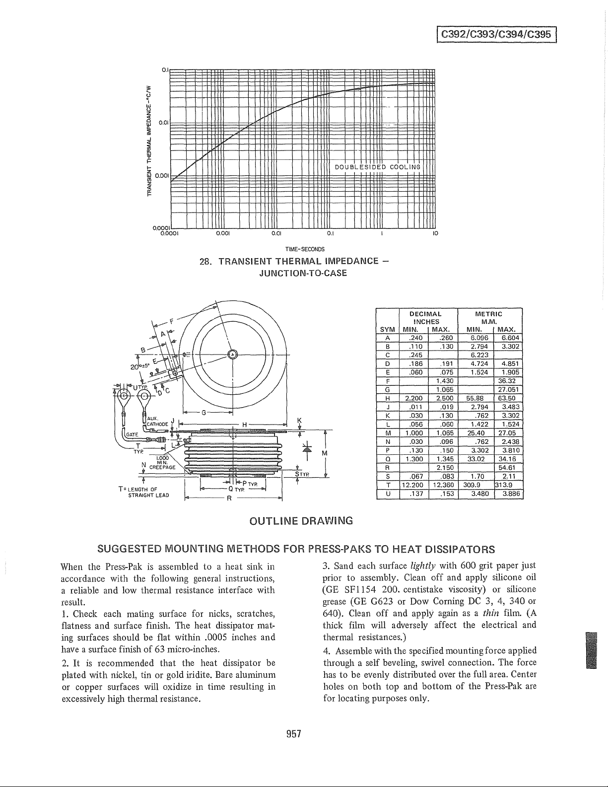
28.
TRANSIENT
0.01
TIME-SECONDS
THERMAL
OOUBLESIOEO
0.1
IMPEDANCE -
..
..
COOLING
10
JUNCTION-TO-CASE
SYM
A
B
C
D
E
F
G
H
J
I<
L
M
N
p
Q
R
S
T
U
DECIMAL
!NCHES M.M.
MIN.
MAX.
.240 .260
.110
.130
.245
.186
.060
2.200 2.500
.011
.030
.056 .060
1.000
.030
.130 .150
1.300
.067
12.200
.137
.191
.075
1.430
1.065
.019
.130
1.065
.096 .762
1.345
2.150
.083
12.360
.153
METRIC
MIN.
55.88
25.40
33.02
309.9 313.9
MAX.
.762
6.604
3.302
4.851
1.905
36.32
27.051
63.50
3.483
3.302
1.524
27.05
2.438
34.16
54.61
2.11
6.096
2.794
6.223
4.724
1.524
2.794
1.422
3.302 3.810
1.70
3.480 3.886
OUTLINE
When the Press-Pak
MOUNTING
is
assembled to a heat sink in
METHODS
accordance with the following general instructions,
a reliable and low thermal resistance interface with
result.
1.
Check each mating surface for nicks, scratches,
flatness and surface finish. The heat dissipator mating
surfaces should be flat within .0005 inches and
have a surface finish
2.
It
is
recommended that the heat dissipator be
of
63
micro-inches.
plated with nickel, tin or gold iridite. Bare aluminum
or
copper surfaces will oxidize in time resulting in
excessively high thermal resistance.
DRAWING
FOR PRESS-PAKS TO
3.
Sand each surface lightly with 600 grit paper just
prior to assembly.
(GE
SFll54
200. centistake viscosity) or silicone
grease (GE G623 or Dow
640). Clean off and apply again
thick film will adversely affect the electrical and
thermal resistances.)
4.
Assemble with the specified mounting force applied
through a self beveling,
has to be evenly distributed over the full area. Center
holes on
both
for locating purposes only.
957
HEAT
DISSIPATORS
Clean off and apply silicone oil
Corning
swivel
top and bottom
DC
3, 4, 340
as
a thin
connection. The force
of
the Press-Pak
film.
or
(A
are
 Loading...