


Semiconductor
2.4GHz 11Mbps MACless DSSS Radio HWB1151 User’s Guide
[ /Title
(AN983
5)
/Subject
(2.4GHz
11Mbps
MACles
s DSSS
Radio
HWB11
51
User’s
Guide)
/Author
()
/Keywords
(Harris
Semiconductor,
PRISM,
Wireless
Communications,
RF,
Radio
Frequency,
IF,
Intermediate
Frequency,
Wire-
Application Note February 1999
The Radio Card product provides all
the hardware required to implement
wireless communication using Direct
Sequence Spread Spectrum (DSSS)
technology. Only an external Media
Access Controller is required.
DSSS technology providesinterferencerejectioninthepresence
of narrow band noise. Since the output power is spread across
such a large bandwidth, the DSSS signal is low level and wide
bandwidth and therefore not intrusive to other equipment.
Evaluation kits include two MACless cards in a PCMCIA Type
II form factor and this application note. TheHWB1151-KIT
MACless radio kit does not include any software .
THE PCMCIA BUS INTERFACE HAS NOT BEEN
IMPLEMENTED IN THIS CARD, THEREFORE A PROPER
INTERF ACE IS REQUIRED , (SEE SIGNALDESCRIPTION).
This product has been designed to allow evaluation of the
Harris PRISM™ Direct Sequence chip set.
The HWB1151-KIT is not FCC approved as an intentional
radiator and is intended for use with cabled connections only
(30dB attenuation recommended antenna port to antenna
port). An FCC experimental license is required while
transmitting over the air with unapproved equipment.
Packaging
AN9835
Author: Richard L. Abrahams
Features
• Provides Antenna-to-Bits™ Data Stream
• Single Heterodyne Conversion
• Autonomous Half Duplex Direct Sequence Modem
• Selectable CCK, MBOK DBPSK and DQPSK Signalling
• Antenna Diversity Selection
• Differential Data Encoding/Decoding
• Programmable 11-Bit PN Code
• Data Rates Up to 11Mbps
• Power Management Control
• Low Profile PCMCIA PC Card Type II
Ordering Information
PART NUMBER DESCRIPTION CARDS PER KIT
HWB1151-EVAL Point-to-Point
Evaluation Kit
HWB1151-EVALPAK System Evaluation
Kit
2
10
2-273
1-800-4-HARRIS or 407-727-9207 | Copyright © Harris Corporation 1999
PRISM® is a registered trademark of Harris Corporation. PRISM logo is a trademark of Harris Corporation.
Antenna to Bits™ is a trademark of Harris Corporation.
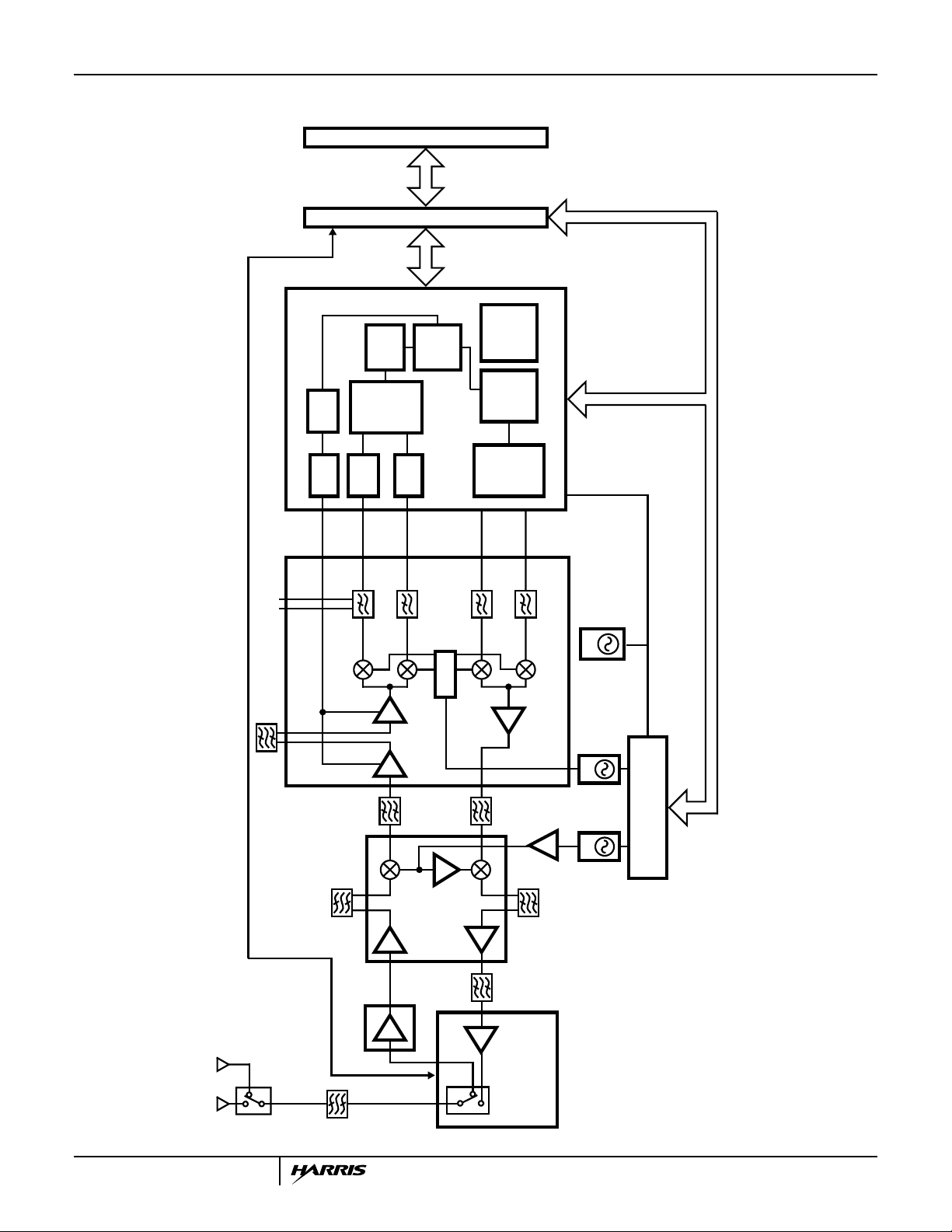
HWB1141 Block Diagram
Application Note 9835
PCMCIA CONNECTOR
BUFFER
SELECT
FILTER CUTOFF
CCA
ADC
RSSI
HFA3726
Q MODEM
DEMOD
QUADRATURE
I ADC
RXI
DE-
MOD
DE-
SPREAD
TX/RX
Q ADC
RXQ
CONTROL
IO
DAT A
TX/RCV
HFA3860B
BASEBAND
PROCESSOR
TXI
FILTERS
LOW PASS
5TH ORDER
BUTTERWORTH
I/Q LO
TEST
CONTROL
MOD/
ENCODE
SPREAD
TXQ
I/O
MODULATOR
QUADRATURE
SERIAL BUS SIGNALS
44MHz
OSC
2-274
TX/RX
CONTROL
ANTENNA
DIVERSITY
SWITCH
LNA
HFA3424
LIMITING IF /RSSI
RF/IF
HFA3624
CONVERTER
HFA3424
HFA3925
RF POWER AMP
BUFFER
SWITCH
AND TX/RX
VCO
VCO
HFA3524A
DUAL SYNTHESIZER
Application Note 9835
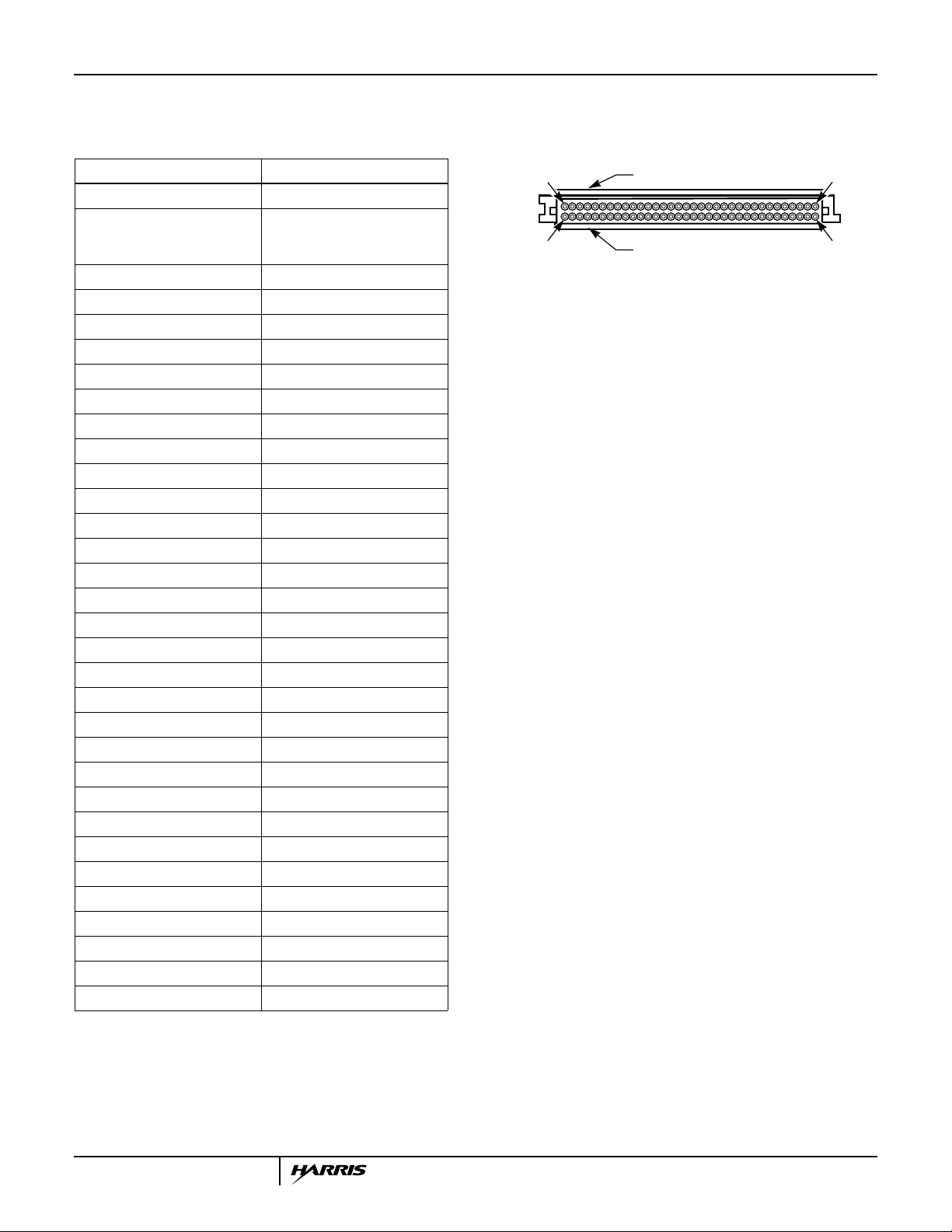
Connector Pin Assignments:
NOTE: Digitalsignalspreceded by “C_” (e.g. C_BB_CS) are CMOS (5V logic) signals. Others are 3.5V logic signals. Data lines are routed through
bi-directional level converters to change from 3.5V to 5V logic levels and vice versa.
SIGNAL NAME PCMCIA PIN NUMBER
GND 1, 34, 35 and 68 Unused 2-10, 13, 15, 16, 18, 22, 23, 31,
32,37,47,49,50, 52-58, 60,61,
64-66
C_OSC_START 11
C_RX_PE_BB 12
C_BB_CS 14
V
CC
C_R_WB 19
C__SPCLK 20
C_SYNTH_LE 21
C_RADIO_PE 24
C_PA_PE 25
C_RESET_BB 26
C_RX_PE 27
C_TXD 28
C_TX_PE 29
C_SPD 30
C_TXC 33
C_RXCIN 36
C_Test_CK 38
C_Test7 39
C_Test6 40
C_Test5 41
C_Test4 42
C_Test3 43
C_Test2 44
C_Test1 45
C_Test0 46
C_SYNTH_LD 48
C_MD_RDY 59
C_CCA 62
C_RXDATA 63
C_TX_RDY 67
17 and 51
PIN 34
PIN 68
VIEW, LOOKING INTO 68 PIN FEMALE CONNECTOR
TOP (LED, THIS SIDE)
BOTTOM
PIN 1
PIN 35
2-275

Application Note 9835
Operating Conditions
Voltage. . . . . . . . . . . . . . . . . . . . . . . . . . . . . . . . . . . . . . 4.5V to 5.5V Temperature Range. . . . . . . . . . . . . . . . . . . . . . . . . . . . 0oC to 55oC
CAUTION: Stresses above those listed in “Absolute Maximum Ratings” may cause permanent damage to the device. This is a stress only rating and operationofthe
device at these or any other conditions above those indicated in the operational sections of this specification is not implied.
DC Electrical Specifications
PARAMETER TEST CONDITIONS MIN TYP MAX UNITS
CURRENT CONSUMPTION
Average Current
Without Power Saving Mode [3] 2% Transmit, 98% Receive - 225 - mA
With Power Saving Mode [3] 2% Transmit, 8% Receive, 90% Standby - 53 - mA
Continuous Receive Mode [3] - 221 - mA
Continuous Transmit Mode [3] - 422 - mA
Standby Mode [3] -30-mA
INPUT/OUTPUT CHARACTERISTICS
Input LOW Level - - 0.8 V
Input HIGH Level 2.0 - - V
Output LOW Level
VOL (IOL = 0.1mA) - - 0.2 V
VOL (IOL = 24mA) - - 0.5 V
Output HIGH Level
VOH (IOH = -3mA) 2.4 3.0 - V
VOH (IOH = -0.1mA) VCC-0.2V - - V Input LOW Current (VCC = Max) - - ±5 µA Input HIGH Current (VCC = Max) - - ±5 µA Output Capacitance - - 8.0 pF Input Capacitance - - 8.0 pF
RF SYSTEM CHARACTERISTICS
Output Power 25oC 14 18 - dBm Transmit Spectral Mask At First Sidelobe - -32 - dBc Receive Sensitivity
1Mbps DBPSK 8% PER - -89 - dBm
2Mbps DQPSK 8% PER - -86 - dBm
5.5Mbps CCK 8% PER - -86 - dBm
11Mbps CCK 8% PER - -83 - dBm Input Third Order Intercept - -22 - dBm Image Rejection 8% PER - 65 - dB IF Rejection 8% PER - 80 - dB Adjacent Channel Rejection 8% PER at 25MHz Offset - 63 - dB
2-276

Application Note 9835
Functional Overview
The Radio Card is based on the Harris PRISM Direct
Sequence Chip Set.
There are ten basic units in this card:
1. Baseband Processor 6. Low Noise Amplifier (LNA)
2. Modulator/Demodulator 7. RF VCO
3. Dual Synthesizer 8. IF VCO
4. Up/Down Converter 9. Antenna
5. Power Amplifier 10. Buffer Interface
During transmission, the data to be transmitted should be
placed on the TX data line going into the baseband processor.
This data will be modulated according to the format selected
(CCK, MBOK, DBPSK or DQPSK) and then spread using a
programmable PN code. Two signals will be generated (I & Q).
The I & Q signals are sent to the Modulator/Demodulator where
they will be first filtered and then modulated with the IF
frequency (280MHz). The IF oscillator generates 560MHz
which is divided by two inside the Modulator/Demodulator , so
the final IF signal is 280MHz. Next, the two signals are
combined into a single signal and sent over to the Up/Down
converter.
The Up/Down converter will shift this signal to the RF
channel programmed in the synthesizer, in the 2.4GHz ISM
band.
In the final stage this signal is amplified to produce a typical
power output of 18dBm, measured in the middle of the ISM
Band at the antenna.
In the receive mode, the radio signal is received by one of
the two external antennas. The antenna selected is optionally determined by an Antenna Diversity algorithm in the
Baseband Processor which compares the quality of the
received signal in each antenna during the Preamble and
selects the better signal. This substantially improves the
multipath performance of the assembly. Alternately, the
antenna selection may be directly controlled by the software.
The signal is amplified by the LNA, and then sent to the
Up/Down converter. The Up/Down converter down-converts
this signal from the 2.4GHz range to the IF frequency,
280MHz.
The Modulator/Demodulator converts the signal to
baseband and splits the signal into the In-Phase (I) and
Quadrature (Q) components, before it is sent to the
Baseband Processor.
Finally, the Baseband Processor despreads and
demodulates the data from DBPSK or DQPSK form, and
places it on the RX data line.
The bi-directional Buffer Translators are used to interface
between computer 5V and card 3.5V logic.
The RF and IF Local Oscillator signals are generated using
the synthesizer and the voltage controlled oscillators. The
dual synthesizer should be programmed with the desired RF
channel frequency less the IF frequency.
Example:
RF IF LO
CH1 2412MHz - 280MHz = 2132MHz
The baseband processor and the synthesizer are driven
from a common 44MHz oscillator to control the timing of
these chips.
Refer to Application Note AN9624 [1] for a more detailed
radio description.
Edge Connector Pin Descriptions
The block diagram in Figure 1 shows control signal
connections from the edge connector to the radio integrated
circuits.
POWER AMP
HFA3925
TX_PE
PA_PE
TX_DATA
TXC
TX_RDY
CCA
RESET_BB
RADIO_PE
RXDATA
RXCIN
MD_RDY
RX_PE_BB
BB_CS
BB_AS
BB_RD/WR
CLK/SYNTH_CLK
SD/SYNTH_DATA
SYNTH_LE
TX_PE
RX_PE
FIGURE 1. CONTROL SIGNAL CONNECTIONS
2
3
4
5
32
35
36
34
33
9
23
8
24
25
11
12
13
22
41
21
43
54
74
15
28
TXD
TXCLK
TX_RDY
CCA
RESET28
RXD
RXCLK
MD_RDY
RX_PE
CS
AS
R/W
SCLK
SD
CLOCK
DAT A
LE
LPF_TX_PE
MOD_TX_PE
LPF_RX_PE
MOD_RX_PE
LIM2_PE
LIM1_PE
TX_PE
RX_PE
UP/DOWN CONVERTER
BASEBAND
PROCESSOR
HFA3860B
SYNTHESIZER
HFA3524A
MOD/DEMOD
HFA3726
HFA3624
2-277

Application Note 9835
NOTE: Digitalsignals preceded by “C_” (e.g. C_BB_CS) are CMOS
(5Vlogic) signals. Othersare 3.5Vlogic signals.Data lines are routed
through bi-directional levelconverters to change from 3.5V to 5V logic levels and vice versa.
In the Discussion below,(I) refers to an Input signal whereas
(O) refers to an Output.
C_PA_PE (I) Pin 25
When active high the baseband processor and power
amplifier are in transmit mode, otherwise they are in standby
mode (see Figure 6). This signal is usually obtained from a
MAC or a network processor.
The internal transmit state machine will be activated by the
rising edge of PA_PE, the falling edge will deactivate it. The
PA_PE envelopes the transmit data.
This signal switches the power amplifier (PA) from TX to RX
as follows:
PA_PE = high--> TX mode
PA_PE = low --> RX mode
C_TXD (I) PIN 28
This pin is used to transfer serial data or preamble/header
data from a MAC or network processor to the baseband
processor. The LSB is received first and the data is clocked
in the baseband processor at the falling edge of TXC.A data
bit high = “one”.
C_TXC (O) Pin 33
Output clock signal to the MACor network processor used to
input serial data to the baseband processor. The data is
clocked into the baseband processor using the falling edge
of TXC.
C_TX_RDY (O) Pin 67
Output to the MAC or network processor which indicates that
the preamble or header has been generated. This signals
that the baseband processor is ready to receive serial data
for transmitting over the TXDATA serial line from the MAC or
network processor.
TX_RDY signal returnsto the inactive state when the PA_PE
goes low indicating the end of transmission.
C_CCA (O) Pin 62
Clear Channel Assessment signal indicates the availabilityof
the channel for transmission. The CCA algorithm is user
programmable. The detailed operation of this pin may be
foundin the PRISM Baseband Processor data sheet [5]. The
active level of this signal is programmable.
C_RXDATA (O) Pin 63
Output to a MAC or a network processor which transfers
demodulated header information and data in serial format.
The LSB is sent first and is aligned with the MD_RDY signal
(see Figure 7).
C_RXCIN (O) Pin 36
This clock signal is used to serially transfer the header and
data from the RXDATApin to the MACor network processor.
The signal is held low when not transferring data.
C_MD_RDY (O) Pin 59
Signal to a MAC or network processor indicating a data
packet is ready. The signal indicates the data transfer over
the RXD serial line.
C_RX_PE_BB (I) Pin 12
When set high the baseband processor is in receive mode.
C_SPD (I/O) Pin 30
There are two purposes for this pin. In regards to the
baseband processor, this serial line is used to transfer
address and data to and from the baseband processor. The
MSB is always transferred first. In regards to the synthesizer,
the address and data are programmed through this line. The
MSB is always first (see Figures 3 and 4).
C_SPCLK (I) Pin 20
This clock signal is used for serial bus transfers to program
the baseband processor and the synthesizer. The data is
clockedon the rising edge ofthe signal at a maximum rate of
10MHz. Even though, CLK/SYNTH_CLK are low frequency,
rise and fall times of less than 10ns should be observed.
{SD/SYNTH_DATA}
{CLK/SYNTH_CLK}
C_BB_CS (I) Pin 14
An active low signal which enables programming of the
Baseband Processor.
C_R_WB (I) Pin 19
Used to change the direction of the SD/SYNTH_DATA line
while programming the baseband processor. This signal
must be set up prior to the rising edge of CLK/SYNTH_CLK.
A high on this line allows data to be inputted to the
Baseband Processor whereas a low is used to write data
from the Baseband Processor.
C_RESET_BB (I) Pin 26
Active low signal. Baseband processor reset. Must be
inactive during programming. When active RX and TX
functions are disabled (see Figure 5).
C_RADIO_PE (I) Pin 24
This signal, when asserted high, enables the radio card.
Power is applied to all chips.
This signal should be kept high during operation of this card.
C_TX_PE (I) Pin 29
This signal, when asserted high, enables the transmit
section of the Modulator/Demodulator and RF/IF Up/Down
converter circuits.
2-278

Application Note 9835
C_RX_PE (I) Pin 27
This signal, when asserted high, enables the receiver
section of the Modulator/Demodulator and RF/IF Up/Down
converter circuits.
C_SYNTH_LE (I) Pin 21
SYNTH_LE, CLK/SYNTH_CLK and SD/SYNTH_DATA
signals are used to program the synthesizer. SYNTH_LE
latches a frame of 22 bits after it has been shifted by the
CLK/SYNTH_CLK into the synthesizer registers. Please
note that the clock and data lines are shared also by the
baseband processor
C_OSC_START (I) Pin 11
This signal is an active low pulse which ensures start-up of
the VCO (see Figure 5). Some brands of VCO’s will not
reliably start oscillating at low control voltages due to the
reduced tank circuit Q caused by this condition. This line
forces the control pin on the VCO to the +3.5V supply rail to
ensure oscillator start-up. The currently recommended
Motorola KXN1332A VCO does not require activation of this
line.
C_SYNTH_LD (O) Pin 48
Lock detect signal coming back from the synthesizer which
signals an out-of-lock condition in either Phase Lock Loop.
May be used to inhibit transmit under these conditions. High
state when out-of-lock.
C_TEST_CK (I) Pin 38
Clock signal used to read the test data from the Baseband
Processor (see the HFA3860B Data Sheet).
C_TEST7 through C_TEST0 (O) Pins 39-46
Reads out the test data from the Baseband Processor (see
the HFA3860B Data Sheet).
Radio Card Programming
Programming Sequence
1. At power up, set all input signals to default values, see
Table 1.
2. Set signal valuesto baseband processor programming
mode (see Figures 2, 3).
3. Program baseband processor as specified in technical
data sheet. Example is provided below.
4. Set signal values to synthesizer programmingmode (see
Figure 4).
5. Program synthesizeras specified in technical data sheet.
Example is provided below.
6. Start TX or RX sequence.
Important - If power is removed from the card, all set ups
will be lost.
All (I) signals are input signals into this card. These signals
are assumed to be controlled by a MAC (Media Access
Controller) and are to be programmed as specified.
Examples are provided as reference only.
TABLE 1. CONTROL SIGNAL DEFAULT VALUES
CONTROL SIGNAL VALUE
C_PA_PE (I) Low
C_TXD (I) Do Not Care
C_RX_PE_BB (I) Low
C_SPD (I/O) Do Not Care
C_SP_CLK (I) Low
C_R_WB (I) Do Not Care
C_BB_CS(I) High
C_RESET_BB (I) High
C_RADIO_PE (I) High
C_TX_PE (I) Low
C_RX_PE (I) Low
C_SYNTH_LE (I) Low
C_OSC_START (I) High
C_TEST_CLK Do Not Care
2-279

Application Note 9835
C_SPCLK
C_SPD
ADDRESS IN DATA IN
C_R_WB
C_BB_CS
C_RADIO_PE
NOTE: Check baseband processor data sheet for timing details.
FIGURE 2. BASEBAND PROCESSOR CONTROL PORT WRITE TIMING
C_SPCLK
C_SPD
ADDRESS IN DATA OUT
C_R_WB
C_BB_CS
LSB
1234567 012345670
LSB
1234567 01234567
LSBMSBMSB
LSBMSBMSB
C_RADIO_PE
NOTE: Check baseband processor data sheet for timing details.
FIGURE 3. BASEBAND PROCESSOR CONTROL PORT READ TIMING
NEXT 22 BITS
MSB
M20
LSBMSB
M17
C_SPCLK
C_SPD
C_BB_CS
C_RADIO_PE
C_SYNTH_LE
1ST 22 BITS
LSB
M18M19M20 M18M19
C0C1
NOTE: Checksynthesizer data sheet for timing details. When the synthesizer is powering up or coming out from Power Down Mode, some registers
should be writteninto it first; refer to the HFA3524,HFA3524Adata sheet. After that, the synthesizer is in PowerUp mode and it can be programmed
according to the data sheet.
FIGURE 4. SYNTHESIZER PROGRAMMING
C_RADIO_PE
PROGRAM
C_OSC_START
C_RESET_BB
C_TX_PE
100µs
PROGRAM BASEBAND PROGRAM SYNTH
10µs
RADIO ON
800µs MIN 1500µs MAX
10µs
1ms
1ms
TX MODE
2-280
FIGURE 5. PROGRAM SEQUENCE

C_RADIO_PE
C_PA_PE
C_TXC
C_TXD
C_TX_RDY
C_TX_PE
C_RX_PE
C_RX_PE_BB
Application Note 9835
2µs
PREAMBLE-HEADER LSB
FIGURE 6. TX MODE TIMING
2µs
DATA PACKET MSB
C_RADIO_PE
C_RX_PE_BB
C_RX_CIN
C_RX DATA
C_MD_RDY
C_TX_PE
C_RX_PE
2µs
LSB
DATA PACKET MSB
FIGURE 7. RX MODE TIMING
2µs
2-281

Application Note 9835
Programming Examples
HFA3860B Baseband Processor programming, 11Mbsp CCK mode, no Antenna Diversity. NOTE: In CCK mode, it is necessaryto
download data twice, designated
CCK Initial and CCK Final.
TABLE 2. CCK INITIAL DOWNLOAD
REGISTER
NAME HEX VALUE COMMENT
CR1 00 I/O Polarity
CR2 14 TX & RX Control
CR3 02 A/D_CAL_POS Register
CR4 FF A/D_CAL_NEG Register
CR5 82 CCA antenna Control
CR6 80 Preamble Length
CR7 48 Scramble_Tap (RX & TX)
CR8 01 RX_SQ1_ACQ (High) Threshold
CR9 88 RX_SQ1_ACQ (Low) Threshold
CR10 00 RX_SQ2_ACQ (High) Threshold
CR11 98 RX_SQ2_ACQ (Low) Threshold
CR12 01 SQ1 CCA Threshold (High)
CR13 98 SQ1 CCA Threshold (Low)
CR14 01 ED or RSSI Threshold
CR15 98 SFD Timer
CR16 48 I Cover Code
CR17 48 Q Cover Code
CR18 37 Signal Field
CR19 6E Signal Field
CR20 00 TX Signal Field
CR21 00 TX Service Field
CR22 FF TX Length Field (High)
CR23 FF TX Length Field (Low)
CR28 00 Test Bus Address
CR30 00 Test Register 1
CR31 19 RX Control MBOK/CCK
TABLE 3. CCK FINAL DOWNLOAD
REGISTER
NAME HEX VALUE COMMENT
CR05 02 Control
CR16 0A Signal
CR17 14 Signal
2-282

Application Note 9835
Example for synthesizer (HFA3524A or HFA3524) programming CH1 (RF and IF), 44MHz Clock, 1MHz steps.
IF R Counter
LSB MSB
0 0 0 0 1 1 0 1 0 0 0 0 0 0 0 0 0 1 1 0 0 0
C1C2 R 16 17 18 19 20
(Read in MSB First, IFR =1802C0h)
R16 = 1 --> IF positive
R17 = 0 --> Low current
R18 = 0 --> D
R19 = 0, R20 = 0 --> F
IF normal operation
OUT
/LD disable
O
IF N Counter
LSB MSB
1 0 0 0 0 0 0 0 0 1 1 0 0 0 1 0 0 0 0 0 1 0
C1C2 A B P, 20
F
= [(P x B) + A] x 44MHz/R <-- see IF R counter set up for “R” value.
VCO
IF
= [(16 x 023h) + 0] x 44MHz/(2Ch) = 560MHz
VCO
N19 = P = 1 --> /16
N20 = 0 = IF powered
RF R Counter
LSB MSB
0 1 0 0 1 1 0 1 0 0 0 0 0 0 0 0 0 1 1 0 0 0
(Read in MSB First, RFR = 1802C8h)
C1C2 R 16 17 18 19 20
R16 = 1 --> RF positive
R17 = 1 --> High current
R18 = 0 --> D
R19 = 0, R20 = 0 --> F
RF normal operation
OUT
/LD disable
O
RF N Counter
LSB MSB
1 1 0 0 1 0 1 0 0 0 1 0 0 0 0 1 0 0 0 0 0 0
C1C2 A B P, 20
F
= [(P x B) + A] x 44MHz/R
VCO
RF
= [(32 x 42h) + 14h] x 44MHz/(2Ch) = 2.132GHz
VCO
N19 = P = 0 = /32
N20 = 0 = RF powered
Please check synthesizer technical data sheet (HFA3524A or HFA3524) [7] for more information.
TABLE 4. IEEE 802.11 OPERATING CHANNEL FREQUENCIES
FCC/IC CHANNEL
FREQUENCIES
CHANNEL ID
1 2412MHz N/A 2412 MHz N/A 2 2417MHz N/A 2417 MHz N/A 3 2422MHz N/A 2422MHz N/A 4 2427MHz N/A 2427MHz N/A
(U.S.A./CANADA)
MKK CHANNE
FREQUENCIE
(JAPAN)
ETSI CHANNEL
FREQUENCIE
(EUROPE)
FRENCH
CHANNEL
FREQUENCIES
SPANISH
CHANNEL
FREQUENCIES
2-283

Application Note 9835
TABLE 4. IEEE 802.11 OPERATING CHANNEL FREQUENCIES (Continued)
FCC/IC CHANNEL
FREQUENCIES
CHANNEL ID
5 2432MHz N/A 2432MHz N/A 6 2437MHz N/A 2437MHz N/A 7 2442MHz N/A 2442MHz N/A 8 2447MHz N/A 2447MHz N/A
9 2452MHz N/A 2452MHz N/A 10 2457MHz N/A 2457MHz 2457MHz 2457MHz 11 2462MHZ N/A 2462MHz 2462MHz 2462MHz 12 N/A N/A 2467MHz 2467MHz N/A 13 N/A N/A 2472MHz 2472MHz N/A 14 N/A 2484MHz N/A N/A N/A
(U.S.A./CANADA)
MKK CHANNE
FREQUENCIE
(JAPAN)
ETSI CHANNEL
FREQUENCIE
(EUROPE)
FRENCH
CHANNEL
FREQUENCIES
SPANISH
CHANNEL
FREQUENCIES
Antenna
The antenna connectors are the Huber Suhner 82MMCX S50 - 2/111KE. The adapter recommended for SMA
connector is the Huber Suhner 33MMCX - SMA - 50 -1.
Antenna select should be programmed by programming the
HFA3860B (bits 0 through 3 in Configuration Register 5).See
the Radio Card Outline for antenna jack locations.
General Notes
1. This card has been tested and adjusted for operation in
DirectSequenceSpread Spectrum.Operation frequency
is in the 2.4GHz band.
2. Powerspectrumoutput waschecked for CH1, CH6 and
CH11.
3. The power output was calibrated to +15dBm and link test
was conducted. The operation range is estimated to be
150 ft. for indoor use.
4.
Always have a 50Ωload installed in the antenna connectors. If the connector is left open it could cause
permanent damage to the power amplifier.
5. The baseband processor MCLK and the synthesizer are
driven by a 44MHz oscillator. Please use this frequency
when programming either device.
6. If thiscard is insertedinaPCMCIA slot byaccidentit will not
enable card detect, therefore no damage to card will occur.
Abbreviations
(I) = Input to the Radio Card
(O) = Output from the Radio Card
MAC = Media Access Controller
TX = Transmit
References
For Harris documents available on the internet, see web site
http://www.semi.harris.com/
Harris AnswerFAX (407) 724-7800.
[1]
AN9624 Application Note
“PRISM1KIT-EVAL DSSS PC Card Wireless LAN
Description”, Carl Andren, Mike Paljug, and Doug
Schultz (Integrated RF Solutions, Inc.), AnswerFAX
Doc. No. 99624.
[2] “2.4GHz Direct Sequence Wireless LAN Cascade
Analysis”, Robert Rood, Doug Schultz, Proc. of the
Sixth Annual Wireless Symposium, pp. 532-540.
[3]
AN9665 Application Note
“PRISM™ Power Management Modes” Carl Andren,
Tim Bozych, Bob Rood and Doug Schultz (Integrated
RF Solutions, Inc.), AnswerFAX Doc. No. 99665.
[4]
AN9790 Application Note
“PRISM1KIT-EVALPC CardWireless LANEvaluation Kit
User’s Guide” Bill Garon, Ans w erFAX Doc. No. 99790.
[5]
HFA3860B Data Sheet
Sequence Spread Spectrum Baseband Processor”,
AnswerFAX Doc. No. 94594.
[6]
AN9617 Application Note
“Hardware/Software Interface Description for PRISM™
Radio Design with an Example Using the AM79C930
Media Access Controller”, John Fakatselis and Mike
Paljug, AnswerFAX Doc. No. 99617.
[7]
HFA3524, HFA3524AData Sheet
Semiconductor, “2.5GHz/600MHz Dual Frequency
Synthesizer”, AnswerFAX Doc. No. 94062.
, Harris Semiconductor,
, Harris Semiconductor,
, Harris Semiconductor,
, Harris Semiconductor, “Direct
, Harris Semiconductor,
, Harris
RX = Receive
High = 5V
Low = 0V
LSB = Least Significant Bit
MSB = Most Significant Bit
2-284

Radio Card Outline - Top View
Application Note 9835
ANTENNA
CONNECTOR
PCMCIA
CONNECTOR
NOTE: A and B refer to Baseband Processor HFA3860B data sheet [5], J1 and J2 (refer to HWB1151-EVAL schematic).
POWER LED
ANTENNA
CONNECTOR
Radio Card Dimensional Outline
A, J2 (NOTE)
B, J1 (NOTE)
NOTE: Units are in millimeters.
2-285
 Loading...