

Page 1

Service Manual
Model #: PD-42S(PLA-4260)
Petters Consumer Brands
4400 Baker Road Minnetonka, MN 55343 U.S.A.
TEL : +952-936-5206 FAX : +952-975-4059
Top Confidential
Page 2

Table of Contents
CONTENTS PAGE
Sections
1. Features 1-1
2. Specifications 2-1
3. On Screen Display 3-1
4. Factory Preset Timings
5. Pin Assignment
4-1
5-1
6. PDP Block Diagram 6-1
7. Control Board Internal I/O Connections 7-1
8. Remove the Burn-in mark 8-1
9. PDP Trouble Shooting 9-1
10. Spare Parts List 10-1
11. Complete Parts List 11-1
Appendix
1. Main Board Circuit Diagram
2. Main Board PCB Layout
3. Assembly Explosion Drawing
Block Diagram
PD-42S (PLA-4260) Service Manual
Page 3

Polaroid Service Manual
PD-42S (PLA-4260)
COPYRIGHT © 2000 .
IBM and IBM products are registered trademarks of International Business Machines
Corporation.
Macintosh and Power Macintosh are registered trademarks of Apple Computer, Inc.
Petters and Petters products are registered trademarks of Petters Consumer Brands.
VESA, EDID, DPMS and DDC are registered trademarks of Video Electronics Standards
Association (VESA).
Energy Star is a registered trademark of the US Environmental Protection Agency (EPA).
No part of this document may be copied, reproduced or transmitted by any means for any
purpose without prior written permission from Petters.
FCC INFORMATION
This equipment has been tested and found to comply with the limits of a Class B digital device,
pursuant to part 15 of the FCC Rules. These limits are designed to provide reasonable
protection against harmful interference in a residential installation. This equipment generates,
uses and can radiate radio frequency energy, and if not installed and used in accordance with
the instructions, may cause harmful interference to radio communications. However, there is
no guarantee that the interference will not occur in a particular installation. If this equipment
does cause unacceptable interference to radio or television reception, which can be
determined by turning the equipment off and on, the user is encouraged to try to correct the
interference by one or more of the following measures -- reorient or relocate the receiving
antenna; increase the separation between equipment and receiver; or connect the into an
outlet on a circuit different from that to which the receiver is connected.
FCC WARNING
To assure continued FCC compliance, the user must use a grounded power supply cord and
the provided shielded video interface cable with bonded ferrite cores. Also, any unauthorized
changes or modifications to Amtrak products will void the user’s authority to operate this
device. Thus Petters Will not be held responsible for the product and its safety.
CE CERTIFICATION
This device complies with the requirements of the EEC directive 89/336/EEC with regard to
“Electromagnetic compatibility.”
SAFETY CAUTION
Use a power cable that is properly grounded. Always use the AC cords as follows – USA (UL);
Canada (CSA); Germany (VDE); Switzerland (SEV); Britain (BASEC/BS); Japan (Electric
Appliance Control Act); or an AC cord that meets the local safety standards.
PETTERS CONSUMER BRANDS ALL RIGHTS RESERVED.
PD-42S (PLA-4260) Service Manual
Page 4

Chapter 1 Features
Wall-mountable
New WIDE XGA Plasma Panel:1024 x 768 (H x V)
Piano finish
Removable speaker system
Extremely thin: less than 100 mm
Fan-less
CONFIDENTIAL – DO NOT COPY
Page 1-1
File No. SG-0159
Page 5

Chapter 2 Product Specification
1. CHARACTERISTICS of PDP module
Type: WXGA PLASMA DISPLAY
Size: 42 inch
Panel: Samsung S42AX-XD02
Active Screen Size (diagonal):42.32 inches (1,074.91mm)
Outline Dimension: Width 1015mm X Height 613mm X Thickness 67.5 mm
Pixel Pitch : 0.912 mm (H) X 0.693mm (V)
Color Depth 16.77M colors
Power Consumption 380 W + 10% (max)
Weight: 21kgs
2. Optical Characteristics
2-1 Viewing Angle > 160° (horizontal) / > 160° (vertical)
2-2 Contrast ratio (panel spec) 3000:1 (Typical)
(w/glass filter) 1500:1 (Typical)
3. System connection connectors
24-pin DVI-D, 20-pin DFP
4. POWER SUPPLY
Input voltage: 100-240Vac, 50/60Hz
Input current: 4A or less (at AC 120V/60Hz)
Inrush current: 60A at Vac=120V
Power consumption: 420 watts (max)
Stand-by: 5 watts max. (at 120 Vac)
Leakage current: No more than 1.3mA at 254Vac/50Hz for universal version
5. Speaker
a. Impedance: 8 Ohm +/- 15%
b. Frequency Range: 75 – 20K Hz
c. Power Input: 15W (max) x2
d. Terminal type: Push switch – polarity: positive (+)/red; negative (-)/black
CONFIDENTIAL – DO NOT COPY
Page 2-1
File No. SG-0159
Page 6

6. ENVIRONMENT
a. Operating temperature: 5~35℃
b. Non-operating temperature: -5~50℃
c. Operating humidity: 20%~70% RH (No condensation)
d. Non-operating humidity: 20%~90% RH (No condensation)
e. Operating altitude: 0~6,560 ft
f. Non-operating altitude: 0~6,560 ft
7. OUTLINE DIMENSIONS (with speaker and base)
a. Height: 820mm
b. Width: 1095mm
c. Depth: 285 mm
8. WEIGHT (with speaker and base)
a. Net: 49.8 kgs +/- 0.5 kgs
b. Gross: 66+/- 0.5 kgs (packed together with set-top box)
9. Warning/Caution/Notice
To prevent possible danger, damage and bodily harm, please consider and observe all
warnings and cautions contained in this paragraph while handling the product or PDP
module only.
This product/PDP module is composed of various kinds of materials such as glass panel,
metals and plastics. A qualified service technician is required for the disposal of the
module.
9.1 Warning
If you do not consider the following warnings, it could result in death or serious injury.
(1) Do not use any other power supply voltage other than the voltage specified in this
product specifications. If you use power voltage deviated from the specifications, it
could result in product failure.
(2) Do not operate or install under the deviated surroundings from the environmental
specification set for the below; in moisture, rain or near water-for example, bath tub,
laundry tub, kitchen sink; in a wet basement; or near a swimming pool; and also near
fire or heater - for example, near or over radiator or heat resistor; or where it is
exposed to direct sunlight; or somewhere like that. If you use the product/PDP module
in places mentioned above, it could result in electric shock, fire hazard or product
failure.
CONFIDENTIAL – DO NOT COPY
File No. SG-0159
Page 2-2
Page 7

(3) If any foreign objects (e.g. water, liquid and metallic chip or dust) entered the
product/PDP module, the power supply voltage to the product/PDP module must be
turned off immediately. Also, never push objects of any kind into the PDP module as
they may touch dangerous voltage point or make short circuits that could result in fire
hazard or electric shock.
(4) If smoke, offensive smell or unusual noise should come from the product/PDP Module,
the power supplymust be turned off immediately. Also, when the screen fails to display
any picture after the power-on or during operation, the power supply must be turned
off immediately. Do not continue to operate the product/PDP module under these
conditions.
(5) The PDP module is controlled by high voltage about 350V. If you need to handle the
module during operation or just after power off, you must take proper precautions
against electric shock and must not touch the drive circuit portion and metallic part
within 5 minutes. The capacitors in the drive circuit portion remain temporarily
charged even after the power is turned off. After turning off the power, you must be
sure to wait at least one minute before touching the module. If the remain voltage is
strong enough, it could result in electric shock.
(6) Do not disconnect or connect the PDP module’s connector while the power is on, or
immediately after power off. Because the module is operated by high voltage, and the
capacitors in drive circuit remain temporarily charged even after the power is turned
off. If you need to disconnect or reconnect it, you have to wait at least one minute
after power off.
(7) Do not disconnect or connect the power connector by a wet hand. The voltage of the
product/PDP module may be strong enough to cause an electric shock.
(8) Do not damage the power cable. Do not modify it either.
(9) When the power cable or connector is damaged or frayed, do not use it.
(10) When the power connector is covered with dust, please wipe it out with a dry cloth
before the power on.
CONFIDENTIAL – DO NOT COPY
File No. SG-0159
Page 2-3
Page 8

9.2 Caution
If you do not consider the following cautions, it may result in personal injury or damage
(1)Do not set the product/PDP module on an unstable place, vibrating place and inclined
place. The product/PDP module may fall or collapse, and it may cause serious injury
to a person, and serious damage to the product.
(2) If you need to move the product/PDP module to another place, you must turn off the
power supply and detach the interface cable and power cable from the product/PDP
module beforehand. If the cables are damaged during the transport, it may result in
fire hazard or electric shock. Also if the product/PDP module has dropped or fallen,
it may cause a serious injury to a person.
(3) When you draw or insert the cables, you must turn off the power and do it by holding
the connector. If you forcibly draw the cable, the electric wire in the cable can be
exposed or broken. It may result in fire hazard or electric shock.
(4) When you carry the product/PDP module, it should be done by at least two persons in
order to avoid any unexpected accidents.
(5) When you carry the product, do not hold the speaker and the bottom of black front
bezel to avoid any injuries to a person or damage to the product.
(6) When you detach the speaker net, do not hold the net surface to avoid deformation.
Please hold the edges.
(7) The product has a glass filter on it and the PDP module has a glass-plate. If the
product/PDP module is inflicted with excessive stress – for example: excessive shock,
vibration, bending or heat-shock, the glass could be broken. It may result in a
personal injury. Also, do not press or strike the glass surface.
(8) If the glass is broken, do not touch it with bare hand.
(9) Do not place any objects on the glass panel. It may be the cause of the scratch or
breakage.
CONFIDENTIAL – DO NOT COPY
File No. SG-0159
Page 2-4
Page 9

(10) When the black front bezel of the product is covered with dust, please use a dry cloth
to wipe it off and afterwards may apply water or a natural detergent to a piece of soft
cloth or gauze, and wring the cloth tightly to clean.
9.3 Additional notice to the operation and handling of the PDP module
(1) To prevent defect or failure, please check the cable connections and power-supply
condition before power on.
(2) To ensure reliable operation of the module and to protect it from overheating, do not
wrap or cover it with a cloth or like a sheet during power-on. Also don not place the
module in a confined space or any other places of poor ventilation.
(3) The screen is controlled with the display-data signals and synchronized signals. If
noise interferes with those signals, the screen could become unstable and in some
case would cause a failure. Do not place any equipment that generates excessive
EMI/RFI noise near the interface cable of the module.
(3) Be careful not to break the glass panel when you handle the module. Also when
handling the module, you must wear gloves or other hand protection to prevent
injuries that can occur in case the glass is broken.
(4) The glass panel section and drive circuit section of the module are closely connected
and they function as a pair. If the module is arbitrarily recombined, restructured, or
disassembled. AmTRAN will not be responsible for the function, quality or operational
integrity of the modified module. Please do not recombine, restructure, or
disassemble it.
(5) To avoid a possible electric shock, you must make sure that the power supply of this
module is turned off before cleaning. To clean the module’s panel, apply water or a
natural detergent to a piece of soft cloth or gauze, and wring the cloth tightly before
wiping the screen. Make sure that no water comes in contact with the connecting
terminals on the side of the glass panel. Do not use chemical solvents, such as
painter thinner or benzene to clean the glass panel.
CONFIDENTIAL – DO NOT COPY
File No. SG-0159
Page 2-5
Page 10

(6) When storing the module, you must select an environmentally controlled space.
Avoid any environment in which the temperature or humidity exceeds the
specification values. If you are storing the module for a long period of time, we
recommended that you place the module together with a dehumidifying agent, such
as silica gel, in a moisture-proof bag and keep it in an environmentally controlled
place.
9-4 Notice to handling the glass filter
(1) When the protection film is peeled off, static electricity is generated between the film
and polarizer. This should be peeled off slowly and carefully by people who are
electrically grounded and with wellion-blown equipment or in such a condition, etc.
(2) To clean the glass filter, you may follow the methods of PDP module mentioned
above.
CONFIDENTIAL – DO NOT COPY
Page 2-6
File No. SG-0159
Page 11

Chapter 3 On Screen Display
Main unit button
STANDY/ON
VOLUME +
VOLUME -
CHANNEL +
CHANNEL -
INPUT
OSD Adjustment
Inputs
PC
DVI-HDCP
VIDEO 1
VIDEO 2
VIDEO 3
VIDEO 4
VIDEO 5
TV
1. VIDEO
2. PC
A. PICTURE MODE
1. MOVIE
2. STANDARD
3. VIVID
4. SPORTS
B. BRIGHTNESS (0~100) (default:50)
C. CONTRAST (0~100) (default:50)
D. SATURATION (0~100) (default:50)
E. HUE (-50~50) (default:0)
F. SHARPNESS (0~14)
A. AUTO( YES/NO)
B. COLOR TEMP (WARM/NORMAL/COOL)
C. CLOCK (0~100)
D. PHASE (0~255)
E. POSITION
1. X (0~100,step 1)
2. Y(0~100,step 1)
CONFIDENTIAL – DO NOT COPY
Page 3-1
File No. SG-0159
Page 12

3. AUDIO
A. BASS (0~100)
B. TREBLE (0~100)
C. BALANCE (-10~10)
D. SRS TS XT (OFF/ON)
4. PIP A. PIP POSITION
B. PIP SIZE
5. TV
1. X (0~100, step:1)
2. Y (0~100, step:1)
1. OFF
2. SMALL
3. MEDIUM
4. PBP
A. SYSTEM
1. ANTENNA
2. STANDARD - CABLE
3. HRC - CABLE
4. IRC – CABLE
B. CHANNEL EDIT
1. AUTO PROGRAM
2. ADD
3. DELETE
CONFIDENTIAL – DO NOT COPY
Page 3-2
File No. SG-0159
Page 13

6. PARENTAL
A. LOCK MENU
B.NEW PASSWORD
C. MPAA RATING (NA/ G/ PG/ PG-13/ R/ NC-17/ X)
D. TV PG RATING
1. NONE
2. TV-Y
3. TV – Y7 (F VIOLENCE)
4. TV - G
5. TV – PG (VIOLENCE /SEXUAL CONTENT/FOUL LANGUAGE/
SUGGESTIVE DIA)
6. TV – 14 (VIOLENCE/ SEXUAL CONTENT/ FOUL LANGUAGE/
SUGGESTIVE DIA)
7. TV-MA (VIOLENCE/ SEXUAL CONTENT/FOUL LANGUAGE)
7. SETTING
A. OSD LANGUAGE (ENGLISH/ FRANÇAIS/ESPAÑOL)
B. FIRMWARE VER (Vx.xx)
C. RESTORE DEFAULT (YES/ NO)
D. TRANSPARENCY
E. CC CONTROL (ON/OFF)
F. MODE (CC1/CC2/CC3/CC4/TEXT1/TEXT2/TEXT3/TEXT4)
8. DISPLAY (BOX/ SHADOW)
CONFIDENTIAL – DO NOT COPY
Page 3-3
File No. SG-0159
Page 14

Chapter 4 Factory preset timings
This timing chart is preset for the Digital plasma monitor.
Mode
No.
Resolution
Refresh
Rate
(Hz)
Horizontal
Frequency
(KHz)
Vertical
Sync
Frequency
Polarity
(Hz)
(TTL)
1 1024x768 60 48.363 60.004 N N 65.000 Windows
Remark: 1. N: negative,
2. This device has no scalars. Some DVI cards will lead to 1 pixel shift even with the
same resolution.
Horizontal
Vertical
Sync
Polarity
(TTL)
Pixel
Rate
(MHz)
Remark
CONFIDENTIAL – DO NOT COPY
Page 4-1
File No. SG-0159
Page 15

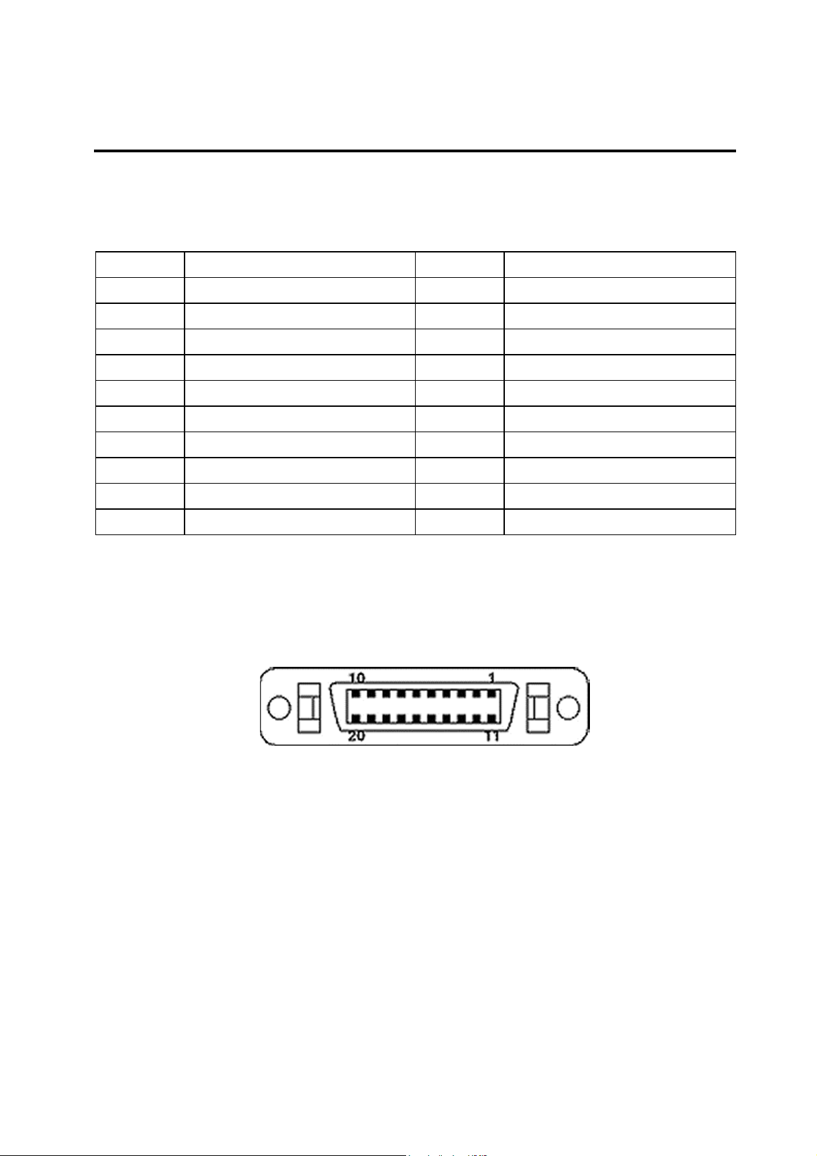
Chapter 5 Pin Assignment
r
p
p
r
p
p
The plasma monitor uses a 24-pin DVI-D connector as a video input interface while connecting to the
PLA-4260 set-top box with a system cable.
Pin Numbe
10 RX1+ TMDS
11 GND Logic Ground
12 Reserved 12 Reserved. No connection
13 Reserved 13 Reserved. No connection
14 VCCX Powe
15 GND Logic Ground
16 SENS SENSE Pin, Pull High
17 RX0- TMDS negative differential input, channel 0
18 RX0+ TMDS
19 GND Logic Ground
20 Reserved 20 Reserved. No connection
21 Reserved 21 Reserved. No connection
22 GND Logic Ground
23 RXC+ TMDS
24 RXC- TMDS negative differential input, reference clock
Signal Name Pin Function
1 RX2- TMDS negative differential input, channel 2
2 RX2+ TMDS
3 GND Logic Ground
4 Reserved 4 Reserved. No connection
5 Reserved 5 Reserved. No connection
6 DDC-CLK DDC2B Clock
7 DDC-DAT DDC2B Data
8 Reserved 8 Reserved. No connection
9 RX1- TMDS negative differential input, channel 1
ositive differential input, channel 2
ositive differential input, channel 1
ositive differential input, channel 0
ositive differential input, reference clock
CONFIDENTIAL – DO NOT COPY
File No. SG-0159
Page 5-1
Page 16
The plasma monitor uses a 20-pin DFP connector as an audio input interface and system control while
connecting to the PLA-4260 set-top box with a system cable.
Pin Number Pin Function Pin Number Pin Function
1 IR 11 Audio_R
2 Ground 12 N.C
3 Ground 13 Ground
4 DB15_Hot Plug 14 +3.3V
5 +5V 15 +5V
6 N.C 16 SDO/TDO (CPLD ISP Pin)
7 TxD 17 SDI/TDI (CPLD ISP Pin)
8 RxD 18 MODE/TMS (CPLD ISP Pin)
9 Audio_L 19 Ground
10 N.C 20 SCK/TCK (CPLD ISP Pin)
Remarks : 16,17,18,20 (CPLD In system programmable)
CONFIDENTIAL – DO NOT COPY
Page 5-2
File No. SG-0159
Page 17
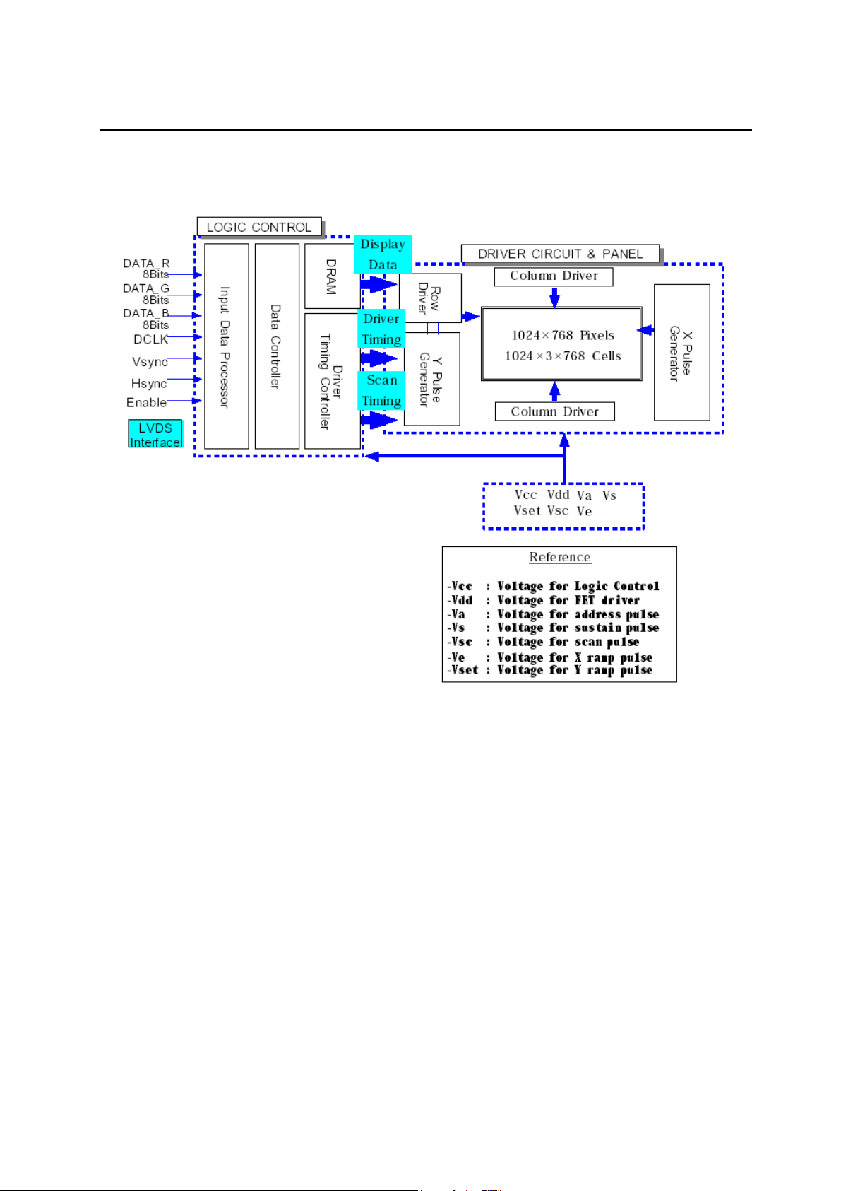
Chapter 6 PDP Block Diagram
System Block Diagram
PDP PANEL
POWER
BOARD
CN9004
LOGIC
BOARD
LA01
CN2
AUDIO
POWER SUPPLY
CN1
EMI
FILTER
AC
INPUT
IR/LED
BOARD
KEYPAD
BOARD
LEFT
J2
W1
W2
W3
J4
J5
SPEAKER
control
board
RIGHT
W5
SYSTEM
W4
W6
DVI_IN
The PDP system block diagram is powered by AC source of 100V~240V AC +/- 10%
@ 50/60 HZ ,another audio power supply that transforms AC source of 100V~240V AC
+/- 10% @ 50/60 HZ into DC 18V source. The DC 18V source supplies the audio AMP
of control board. The digital IC parts of control board is powered by DC 5V from PDP
panel side.
CONFIDENTIAL – DO NOT COPY
File No. SG-0159
Page 6-1
Page 18
PDP panel Block Diagram
CONFIDENTIAL – DO NOT COPY
Page 6-2
File No. SG-0159
Page 19
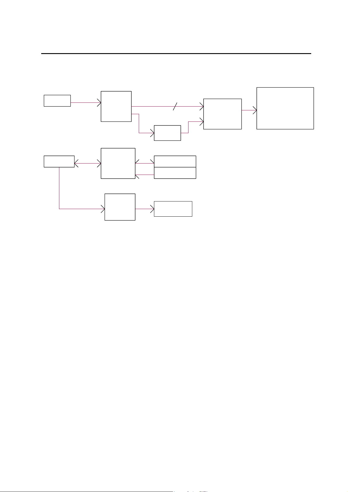
Control board Block Diagram
DVI_IN
SYSTEM_IN
RS232
AUDIO_L/R
DVI
RECEIVER
SIL161
up
SM5964
Audio
amp
TDA8947J
RGB24BIT
HS/VS/DE
CPLD
LC4128V
IR/LED BOARD
SPEAKER
KEYPAD
HS/VS/DE
LVDS
TRANSMITTER
DS90C387
PDP
LOGIC
BOARD
CONFIDENTIAL – DO NOT COPY
Page 6-3
File No. SG-0159
Page 20

Chapter 7 Control Board Internal I/O Connections
W1 CONNECTION (TOP→BOTTOM) "DC POWER INPUT/OUTPUT”
Pin Description
1 “+5VSB_INPUT”
2 “+5VSB_INPUT”
3 “+5VSB_INPUT”
4 “D_GND”
5 “D_GND”
6 “D_GND”
7 “PDP_RELAY_ON”
8 N.C.
W2 CONNECTION (TOP→BOTTOM) “IR/LED_BOARD_CONTROL”
Pin Description
1 “+5VSB_OUTPUT”
2 “IR_DATA_IN”
3 “LED_BLUE”
4 “D_GND”
5 “LED_RED”
6 N.C.
W3 CONNECTION (TOP→BOTTOM) “KEY_PAD”
Pin Description
1 “POWER_KEY”
2 “N.C.”
3 “N.C.”
4 “VOL-_KEY
5 “GND”
6 “VOL+_KEY
CONFIDENTIAL – DO NOT COPY
7 “CH-_KEY
8
9
“CH+_KEY
“SOURCE
Page 7-1
File No. SG-0159
Page 21

W4 CONNECTION (RIGHT->LEFT)”VIDEO(LVDS) SIGNAL TRANSMITION”
Pin Description
1 “D_GND”
2 “N.C.
3 “D_GND”
4 “N.C.”
5 “N.C.”
6 “D_GND”
7 “D_GND”
8 “N.C.”
9 “N.C.”
10 “N.C.”
11 “N . C.”
12 “N.C.”
13 “N.C.”
14 “D_GND”
15 “N.C.”
16 “N.C.”
17 “TXD+”
18 “TXD-“
19 “TXCLK+”
20 “TXCLK-“
21 “D_GND”
22 “TXC+”
23 “TXC-“
24 “TXB+”
25 “TXB-“
26 “TXA+”
27 “TXA-“
28 “D_GND”
29 “D_GND”
30 “D_GND”
CONFIDENTIAL – DO NOT COPY
Page 7-1
File No. SG-0159
Page 22

J2 CONNECTION (RIGHT→LEFT) “AUDIO_POWER_INPUT”
Pin Description
1 “+18V”
2 “+18V”
3 “+18V”
4 “A_GND”
5 “A_GND”
6 “A_GND”
J4 CONNECTION (RIGHT→LEFT) “SPEAKER_OUT”
Pin Description
1 “RIGHT-”
2 “RIGHR+”
J5 CONNECTION (RIGHT→LEFT) “SPEAKER_OUT”
Pin Description
1 “LEFT+”
2 “LEFT-”
CONFIDENTIAL – DO NOT COPY
Page 7-1
File No. SG-0159
Page 23

Chapter 8 Remove the Burn-in mark
To remove burn-in mark on the PDP
1 Be sure the set-top box is connected well.
2 Select TV as main source.
3 Turn off PIP window if any.
4 Press the password on the remote control:
“SWAP” -> “UP” -> “UP” -> “DOWN” -> “DOWN” -> “SELECT”
5 Burn-in mode starts. You will see red, green, blue and white screens display.
Keep them displaying at least 8 hours.
6 Press “EXIT” key to exit the burn-in mode and check if the mark is still visible. If so,
you may carry on the steps from 10.4.
CONFIDENTIAL – DO NOT COPY
Page 8-1
File No. SG-0159
Page 24

Chapter 9 PDP Trouble Shooting
PDP DISPLAY NOTHING(MONITOR ONLY WIHOUT BOX)
START
AC POWER
input ?
DVI has
signal ?
cable ?
DC
power?
SET AC POWER SWITCH TO ON
1.check DVI cable connection
2.set your PC resolution to 1024x768 /60HZ
3.set your PC display card to DVI output
4.set PDP AC switch to OFF then ON
check all internal cable have be connected.internal
1.check U2 input has +5V
2.check U2 output has +3.3V
3.check RELAY_ON signal is low
Hsync,
Vsync,DE
have signal?
END
CONFIDENTIAL – DO NOT COPY
1.check U10 have output Hsync/Vsync/DE signal
2.check U15 have output Hsync/Vsync/DE signal
3.check U7 have output LVDS signal
Page 9-1
File No. SG-0159
Page 25

PDP DISPLAY NOTHING( WITH BOX)
START
AC POWER
input ?
DVI&
SYSTEM
CABLE OK?
internal
cable ?
DC
power?
SET AC POWER SWITCH TO ON
1.check DVI&SYSTEM cable connection
2.check input source what you select
3.set input source to what you select
check all internal cable have be connected.
1.check U2 input has +5V
2.check U2 output has +3.3V
3.check RELAY_ON signal is low
Hsync,
Vsync,DE
have
signal?
END
CONFIDENTIAL – DO NOT COPY
1.check U10 have output Hsync/Vsync/DE signal
2.check U15 have output Hsync/Vsync/DE signal
3.check U7 have output LVDS signal
Page 9-2
File No. SG-0159
Page 26

PDP NO SOUND( WITH BOX)
START
AC POWER
input ?
DVI&
SYSTEM
CABLE OK?
internal
cable ?
DC
power?
SET AC POWER SWITCH TO ON
1.check DVI&SYSTEM cable connection
2.check input source(video&audio) what you select
3.set input source to what you select
check all internal cable have be connected.
1.check U2 input has +5V
2.check U2 output has +3.3V
3.check RELAY_ON signal is low
4.check F1 has +18V
speaker
output?
END
CONFIDENTIAL – DO NOT COPY
1.check U8 have audio input signal
2.check U8 MODE1 pin signal is +18V
3.check Q5 Gate pin has +5V
Page 9-3
File No. SG-0159
Page 27

TROUBLE OF DDC READING
Star t
Yes
Digital DDC OK?
Yes
END
N0
Support DDC2B
1.Digital cable ok?
2.Voltage of VCCX ok?
3.Check U32
5.Is compliant protocol?
CONFIDENTIAL – DO NOT COPY
Page 9-4
File No. SG-0159
Page 28

Chapter10 Spare Parts List
PD-42S / PLA-4260
PART NO DESCRIPTION LOC QTY REMARK
0185-1402-0003 FUSE 125V/4A SMD (R451004)
0420-1002-4611 MOSFET N-CH 2N7002 SMD (SOT-23)
0420-2003-1626 MOSFET P-CH 9A 30V P2003EV SOP-8
0430-4009-3109 IC TDA8947J DIP 17PIN
0430-6005-6004 IC LM1117MPX-ADJ SMD 3PIN (SOT-223)
1801-0117-4010 FRONT BEZEL (PD-42S)(ABS, 877C) ASS'Y 1
1925-1000-2150 CUSHION-R (AVC42) 2
1925-1000-2170 EPE FOAM-B (PD-42S) 1
1925-1000-2180 EPE FOAM-T (PD-42S) 1
1925-1000-2430 EPE FOAM-F (PD-42S) 1
1925-1100-1760 PE BAG (1300.0*1200.0*0.4t)(PD-42S) 1
1925-1200-6850 CARTON BLANK (PD-42S) 1
1925-1200-7210 ACCESSARY BOX (366.0L*232.0D*71.0H) 1
1925-1900-0490 GUARDBOARD 40.0*40.0*430.0mm (PD-42S) 4
1947-1200-0400 ACETATE CLOTH TAPE ( 醋酸布膠帶 ) 20*45mm 5
1947-1200-2290 Insulator (300*150*0.25t) 1
F1
Q10,Q2
Q1
U8
U2
1
2
1
1
1
1947-1200-2300 Insulator (8*170*0.25t ) 1
1947-1400-0110 SPEAKER FRONT BEZEL NET (PD-42S) 1
1947-1500-2160 PANEL CUSHION 950.0*10.0*7.0mm (PD-42S) 2
1947-1500-2170 PANEL CUSHION 550.0*10.0*7.0mm (PD-42S) 2
1947-1500-2180 SPONGE (PD-42S) 4
1947-1700-0240 GASKET BLOCK (40*4.0*1.0) 2
1947-1700-1100 GASKET BLOCK (20.0*13.0*10.0) 2
1947-1800-0150 GASKET EMI (17*25*210mm) 6
1947-1800-0240 GASKET EMI (5*1*100mm) 2
1947-1800-0370 GASKET BLOCK (5.5H*10.0W*30.0Lmm) 1
1947-1800-0670 Gasket Block (10W*3H*80L mm) 7
1947-1800-0690 Gasket Block (20W*0.3H*583L mm) 2
1947-1800-0700 Gasket Block (20W*0.3H*983L mm) 2
1947-1800-0710 Gasket Block (17.0W*1.0H*41.0L) 2
1947-1800-0780 Gasket Block (5W*2H*300L) 1
1947-1900-0030 HEATPATH (25x14mm) 1
CONFIDENTIAL – DO NOT COPY
Page 10-1
File No. SG-0159
Page 29

PART NO DESCRIPTION LOC QTY REMARK
1947-2400-0010 SPEAKER LOWER ASS'Y (PD-42S) 1
3842-0012-0154 PDP CONTROL BD ASS'Y (PD-42S)
3842-0012-0307 SWITCH ASS'Y (PD-42S)
3842-0022-0156 PDP DISPLAY BD ASS'Y (PD-42S)
3842-0032-0189 PDP IR BD ASS'Y (PD-42S)
CONFIDENTIAL – DO NOT COPY
Page 10-2
File No. SG-0159
Page 30

Chapter 11 Complete Parts List
Q
)
2842-4203-0004 Plasma monitor 42'' (PD-42S)(ABS,BLACK)
ITEM
1 3842-0022-0301 PDP BASE ASS'Y (PD-42S)(ABS, 877C
2 3842-0022-0303 PDP CHASSIS ASS'Y (PD-42S) 1
3 3842-0022-0312 PDP PACKING ASS'Y (PD-42S) 1
M/S
LOCATION
PART NO. DESCRPTION
TY
1
CONFIDENTIAL – DO NOT COPY Page 11-1
File No. SG-0159
Page 31

3842-0022-0301 PDP BASE ASS'Y (PD-42S)(ABS, 877C)
ITEM
1 1701-0515-1010 Base Cover (PD-42S)(ABS, 5108M) 1
2 1701-1000-0350 BASE FOOT ( φ 30.0mm t=1mm)(PD-42S) 6
3 1712-0100-6790 Base Plate (SECC t=2.2mm)(PD-42S) 1
4 1712-1200-0070 BASE Die (PD-42S) 2
5 1720-1306-1850 MAC. SCREW-MPSW M6.0*18.0L, BLK- Ni 8
6 1720-3006-1550 MAC. SCREW-MF M6.0*15.0L, BLK-Ni 8
7 1721-3047-1220 TAP SCREW-MF #4.7*12.0L, Ni 14
8 1947-1400-0110 SPEAKER FRONT BEZEL NET (PD-42S) 1
9 1947-2400-0010 SPEAKER LOWER ASS'Y (PD-42S) 1
M/S
LOCATION
PART NO. DESCRPTION QTY
CONFIDENTIAL – DO NOT COPY Page 11-2
File No. SG-0159
Page 32

3842-0022-0303 PDP CHASSIS ASS'Y (PD-42S)
ITEM
1 0213-0420-0967 PDP MODULE 42'' S42AX-XD02 (SAMSUNG) 1
2 0220-8020-0881 SW ROCKERSW 250V 6A 2P HF606A1BBATA 1
3 0260-0000-0210 LINE FILTER ASS'Y 6A 06DBDW3S-AM01 1
4 0460-1006-0202 WH PH6P-PH5P 1061#26 600mm CORE*1 SHIELDING 1
5 0460-1009-0411 WH PH9P-PH7P+SRA4.3*2 1061#26 710mm CORE*1 1
6 0460-1106-0160 WH XH6P-XH6P 1007#24 250mm 1
7 0460-1211-0020 WH 35572-11P-XH8P 2P 120mm 1
8 0460-3430-0540 WH FI-W31S/DF14-30S 20276#30 160mm 1
9 0500-0502-0030 POWER BD ASS'Y 18V 4.5A (0432D1881) 1
10 1701-0414-9010 Button (PD-42S)(ABS, 877C) 1
11 1701-0900-1300 Samsung 42'' PDP EMI Filter ,Mesh Type (42S3) 1
12 1701-0900-1350 WASHER (FR63, 0.5t)(F19R31) 4
13 1701-1500-0450 WIRE SADDLE (CH-01B) 8
14 1701-1919-1010 HANDLE (PC+ABS, Black)(PD-42S) 2
15 1712-0100-4590 HEAT SINK FIX MTEAL (TM-30A) 1
M/S
LOCATION
PART NO. DESCRPTION QTY
16 1712-0100-6740 Filter Clip (SECC t=1.0MM)(PD-42S) 10
17 1712-0100-6750 Main Frame Lateral High (SECC t=2.0mm)(PD-42S) 1
18 1712-0100-6760 Main Frame Cross (SECC t=2.0MM)(PD-42S) 2
19 1712-0100-6770 Rear Cover ( SECC t=1.0mm)(PD-42S) 1
20 1712-0100-6780 Flat Metal (SECC t=1.0mm)(PD-42S) 2
21 1712-0100-6930 PCB Supportor (PD-42S)(SECC t=1.0mm) 1
22 1712-0100-6940 I/O Bracket (PD-42S)(SECC t=1.0mm) 1
23 1712-0100-7480 Main Frame Lateral Low (SECC t=2.0mm)(PD-42S) 1
24 1712-0400-0720 HEAT SINK (PD-42S) 1
25 1712-1200-0060 Stand Frame (PD-42S) 2
26 1720-0003-0620 MAC. SCREW-MB M3.0*6.0L,Ni 16
27 1720-0004-1210 MAC. SCREW M4.0*12.0L, Zn-Cc 12
28 1720-1006-0820 MAC. SCREW-MP M6.0*8.0L, Ni 8
29 1720-1204-0820 MAC. SCREW-MPGW M4.0*8.0L,Ni 1
30 1720-1503-0620 MAC.SCREW-MPSWF M3.0*6.0L Ni 4
CONFIDENTIAL – DO NOT COPY Page 11-3
File No. SG-0159
Page 33

ITEM
31 1720-1505-1550 MAC. SCREW-MPSFW M5.0*15.0L, BLK-Ni 4
32 1720-5003-0550 MAC. SCREW-MI M3.0*5.0L, BLK-Ni 9
33 1720-7344-0820 MAC. SCREW-MHSW #4-40*8.0L,Ni 2
34 1721-0003-1050 TAP. SCREW-TB #3*10.0L, BLK-Ni 4
35 1721-0004-1050 TAP. SCREW-TP #4.0*10.0L, BLK-Ni 52
36 1721-5003-0520 TAP. SCREW-TI M3.0*5.0L,Ni 32
37 1801-0117-4010 FRONT BEZEL (PD-42S)(ABS, 877C) ASS'Y 1
38 1812-0100-6690 FilTER BKT ASS'Y (PD-42S) 1
M/S
LOCATION
PART NO. DESCRPTION QTY
39 1947-1200-0400
40 1947-1200-2290 Insulator (300*150*0.075t) 1
41 1947-1200-2300 Insulator (8*170*0.215t) 1
42 1947-1500-2160 PANEL CUSHION 950.0*10.0*7.0mm (PD-42S) 2
43 1947-1500-2170 PANEL CUSHION 550.0*10.0*7.0mm (PD-42S) 2
44 1947-1500-2180 SPONGE (PD-42S) 4
45 1947-1700-0240 GASKET BLOCK (40*4.0*1.0) 2
46 1947-1700-1100 GASKET BLOCK (20.0*13.0*10.0) 2
47 1947-1800-0150 GASKET EMI (17*25*210mm) 6
48 1947-1800-0240 GASKET EMI (5*1*100mm) 2
49 1947-1800-0370 GASKET BLOCK (5.5H*10.0W*30.0Lmm) 1
50 1947-1800-0670 Gasket Block (10W*3H*80L mm) 7
51 1947-1800-0690 Gasket Block (20W*0.3H*583L mm) 2
52 1947-1800-0700 Gasket Block (20W*0.3H*983L mm) 2
53 1947-1800-0710 Gasket Block (17.0W*1.0H*41.0L) 2
54 1947-1800-0780 Gasket Block (5W*2H*300L) 1
ACETATE CLOTH TAPE ( 醋酸布膠帶 ) 20*45mm
5
55 1947-1900-0030 HEATPATH (25x14mm) 1
56 3842-0012-0154 PDP CONTROL BD ASS'Y (PD-42S) 1
57 3842-0012-0307 SWITCH ASS'Y (PD-42S) 1
58 3842-0022-0156 PDP DISPLAY BD ASS'Y (PD-42S) 1
59 3842-0032-0189 PDP IR BD ASS'Y (PD-42S) 1
CONFIDENTIAL – DO NOT COPY Page 11-4
File No. SG-0159
Page 34

3842-0022-0312 PDP PACKING ASS'Y (PD-42S)
ITEM
1 1925-1000-2150 CUSHION-R (AVC42) 2
2 1925-1000-2170 EPE FOAM-B (PD-42S) 1
3 1925-1000-2180 EPE FOAM-T (PD-42S) 1
4 1925-1000-2430 EPE FOAM-F (PD-42S) 1
5 1925-1100-1760 PE BAG (1300.0*1200.0*0.4t)(PD-42S) 1
6 1925-1200-6850 CARTON BLANK (PD-42S) 1
7 1925-1900-0490 GUARDBOARD 40.0*40.0*430.0mm (PD-42S) 4
8 3842-0012-0393 PDP ACCESSORY ASS'Y (PD-42S) 1
M/S
LOCATION
PART NO. DESCRPTION QTY
CONFIDENTIAL – DO NOT COPY Page 11-5
File No. SG-0159
Page 35

3842-0012-0154 PDP CONTROL BD ASS'Y (PD-42S)
ITEM
1 384200120154A PDP CONTROL BD ASS'Y (PD-42S) AI 1
2 384200120154M PDP CONTROL BD ASS'Y (PD-42S) MI 1
3 384200120154S PDP CONTROL BD ASS'Y (PD-42S) SMD 1
M/S
LOCATION
PART NO. DESCRPTION QTY
CONFIDENTIAL – DO NOT COPY Page 11-6
File No. SG-0159
Page 36

3842-0012-0307 SWITCH ASS'Y (PD-42S)
ITEM
1 0220-6020-0186 SW PUSH Terminal DIP 2PIN 2
2 0242-0225-1504 HEAT S-T 2.0*0.25 15MM 125' 4
3 0460-1102-0072 WH XH2P-NC 1007#24 540mm CORE*2 1
4 0460-1102-0082 WH XH2P-NC 1007#24 400mm CORE*2 1
M/S
LOCATION
PART NO. DESCRPTION QTY
CONFIDENTIAL – DO NOT COPY Page 11-7
File No. SG-0159
Page 37

3842-0012-0393 PDP ACCESSORY ASS'Y (PD-42S)
ITEM
1 0320-4000-0140 POWER CORD 1800mm 110V UL/CSA (BLK)(N.M.) 2
2 0321-0000-0251 DVI/D TYPE CABLE 3000mm BLK core*4 1
3 1925-1200-7210 ACCESSARY BOX (366.0L*232.0D*71.0H) 1
M/S
LOCATION
PART NO. DESCRPTION QTY
CONFIDENTIAL – DO NOT COPY Page 11-8
File No. SG-0159
Page 38

3842-0022-0156 PDP DISPLAY BD ASS'Y (PD-42S)
ITEM
1 0170-1740-1182 PCB DISPLAY BD V0 165.0*16.2*1.6t S (PD-42S) 1
2 SWK1 0220-7020-0965 SW TACT 6*6mm 180' 160g SFKHHAM2520 1
3 SWK2 0220-7020-0965 SW TACT 6*6mm 180' 160g SFKHHAM2520 1
4 SWK3 0220-7020-0965 SW TACT 6*6mm 180' 160g SFKHHAM2520 1
5 SWK4 0220-7020-0965 SW TACT 6*6mm 180' 160g SFKHHAM2520 1
6 SWK5 0220-7020-0965 SW TACT 6*6mm 180' 160g SFKHHAM2520 1
7 SWK6 0220-7020-0965 SW TACT 6*6mm 180' 160g SFKHHAM2520 1
8 W1 0451-2000-0766 WAFER 2.00MM 7P 90' KINK (STM) 1
M/S
LOCATION
PART NO. DESCRPTION QTY
CONFIDENTIAL – DO NOT COPY Page 11-9
File No. SG-0159
Page 39

3842-0032-0189 PDP IR BD ASS'Y (PD-42S)
ITEM
1 384200320189A PDP IR BD ASS'Y (PD-42S) AI 1
2 384200320189M PDP IR BD ASS'Y (PD-42S) MI 1
3 384200320189S PDP IR BD ASS'Y (PD-42S) SMD 1
M/S
LOCATION
PART NO. DESCRPTION QTY
CONFIDENTIAL – DO NOT COPY Page 11-10
File No. SG-0159
Page 40

3842-0012-0154A PDP CONTROL BD ASS'Y (PD-42S) AI
ITEM
1 C3 0102-2102-1212 E/C L-L 1000uF/16V 105' NF-T 10*16 (KY) 1
2 SS 0103-6102-1212 E/C HF 1000uF 16V 105'C F (10*20)
3 C5 0103-1471-1211 E/C VZ 470uF 16V 105'C F-T (8*11.5mm) 1
4 C50 0102-2102-1312 E/C L-L 1000UF 25V 105' F (KY TYPE) 1
5 C54 0103-1220-1511 E/C VT 22uF 50V 105'C F-T (5*11mm) 1
6 C56 0103-1229-1511 E/C VT 2.2uF 50V 105'C F-T (5*11mm) 1
7 SS 0101-1229-1511 E/C GEN. 2.2UF 50V 105' F
8 C57 0102-2221-1311 E/C L-L 220uF/25V 105' F 8*11.5 (KY) 1
9 C68 0103-1101-1211 E/C VZ 100uF 16V 105'C F-T (5*11mm) 1
10 C69 0103-1470-1211 E/C VT 47uF 16V 105'C F-T (5*11mm) 1
11 SS 0101-1470-1211 E/C GEN. 47UF 16V 105' F
12 C70 0103-1470-1211 E/C VT 47uF 16V 105'C F-T (5*11mm) 1
13 SS 0101-1470-1211 E/C GEN. 47UF 16V 105' F
14 C8 0103-1101-1211 E/C VZ 100uF 16V 105'C F-T (5*11mm) 1
15 C84 0103-1470-1211 E/C VT 47uF 16V 105'C F-T (5*11mm) 1
M/S
LOCATION
PART NO. DESCRPTION QTY
16 SS 0101-1470-1211 E/C GEN. 47UF 16V 105' F
17 C85 0103-1470-1211 E/C VT 47uF 16V 105'C F-T (5*11mm) 1
18 SS 0101-1470-1211 E/C GEN. 47UF 16V 105' F
19 C86 0103-1470-1211 E/C VT 47uF 16V 105'C F-T (5*11mm) 1
20 SS 0101-1470-1211 E/C GEN. 47UF 16V 105' F
21 D22 0390-6002-8272 SCHOTTKY DIODE 1A 40V SB140 1
CONFIDENTIAL – DO NOT COPY Page 11-11
File No. SG-0159
Page 41

3842-0012-0154M PDP CONTROL BD ASS'Y (PD-42S) MI
ITEM
1 JP1 0455-2540-0479 PIN HEADER 2*2P 2.54mm 180' 1
2 J2 0451-2500-0616 WAFER 2.50MM 6P 180' KINK (STM) 1
3 J4 0451-2500-0216 WAFER 2.50mm 2P 180' KINK (STM) 1
4 J5 0451-2500-0216 WAFER 2.50mm 2P 180' KINK (STM) 1
5 U8 0430-4009-3109 IC TDA8947J DIP 17PIN 1
6 W1 0451-2500-0816 WAFER 2.50MM 8P 180' KINK (STM) 1
7 W2 0451-2000-0606 WAFER 2.00MM 6P 180'KINK 1
8 W3 0451-2000-0906 WAFER 2.00MM 9P 180'KINK (STM) 1
9 W5 0303-5000-2004 CONN D-TYPE 20PIN 1
10 W6 0302-3010-0240 DVI CONN R/A D 24PIN (DV2R024N11) 1
11 Y1 0280-2400-0115 X'TAL 24MHz 49/US 30PPM CL:18PF 1
M/S
LOCATION
PART NO. DESCRPTION QTY
CONFIDENTIAL – DO NOT COPY Page 11-12
File No. SG-0159
Page 42

3842-0012-0154S PDP CONTROL BD ASS'Y (PD-42S) SMD
ITEM
1 0171-2141-0062 PCB CONTROL BD FR4 165.0*150.0*1.6t D (PD-42S) 1
2 CP1 0111-5103-5121 ARRAY CAP 0.01uF 50V X7R 8PIN 1
3 CP2 0111-5103-5121 ARRAY CAP 0.01uF 50V X7R 8PIN 1
4 C100 0112-3471-5106 C/M Multi. 470PF 50V NPO 0603 1
5 C101 0112-3471-5106 C/M Multi. 470PF 50V NPO 0603 1
6 C102 0112-3471-5106 C/M Multi. 470PF 50V NPO 0603 1
7 C21 0112-3104-5116 C/M Muitl. 0.1uF 50V X7R 0603 1
8 C22 0112-3106-1614 C/M MULTI 10uF 16V X7R 1206 1
9 C23 0112-3150-5106 C/M MULTI 15PF 50V NPO 0603 1
10 C24 0112-3150-5106 C/M MULTI 15PF 50V NPO 0603 1
11 C25 0112-3106-1614 C/M MULTI 10uF 16V X7R 1206 1
12 C26 0112-3104-5116 C/M Muitl. 0.1uF 50V X7R 0603 1
13 C27 0112-3104-5116 C/M Muitl. 0.1uF 50V X7R 0603 1
14 C28 0112-3104-5116 C/M Muitl. 0.1uF 50V X7R 0603 1
15 C29 0112-3104-5116 C/M Muitl. 0.1uF 50V X7R 0603 1
M/S
LOCATION
PART NO. DESCRPTION QTY
16 C30 0112-3104-5116 C/M Muitl. 0.1uF 50V X7R 0603 1
17 C31 0112-3104-5116 C/M Muitl. 0.1uF 50V X7R 0603 1
18 C32 0112-3104-5116 C/M Muitl. 0.1uF 50V X7R 0603 1
19 C33 0112-3104-5116 C/M Muitl. 0.1uF 50V X7R 0603 1
20 C34 0112-3104-5116 C/M Muitl. 0.1uF 50V X7R 0603 1
21 C35 0112-3104-5116 C/M Muitl. 0.1uF 50V X7R 0603 1
22 C36 0112-3104-5116 C/M Muitl. 0.1uF 50V X7R 0603 1
23 C37 0112-3104-5116 C/M Muitl. 0.1uF 50V X7R 0603 1
24 C40 0112-3101-5106 C/M Multi. 100PF 50V NPO 0603 1
25 C41 0112-3101-5106 C/M Multi. 100PF 50V NPO 0603 1
26 C42 0112-3101-5106 C/M Multi. 100PF 50V NPO 0603 1
27 C43 0112-3101-5106 C/M Multi. 100PF 50V NPO 0603 1
28 C44 0112-3101-5106 C/M Multi. 100PF 50V NPO 0603 1
29 C45 0112-3101-5106 C/M Multi. 100PF 50V NPO 0603 1
30 C49 0112-3104-5116 C/M Muitl. 0.1uF 50V X7R 0603 1
CONFIDENTIAL – DO NOT COPY Page 11-13
File No. SG-0159
Page 43

ITEM
31 C53 0112-3474-2515 C/M Multi. 0.47UF 25V X7R 0805 1
32 C58 0112-3105-2514 C/M Multi. 1.0uF 25V X7R 1206 1
33 C6 0112-3104-5116 C/M Muitl. 0.1uF 50V X7R 0603 1
34 C65 0112-3104-5116 C/M Muitl. 0.1uF 50V X7R 0603 1
35 C66 0112-3470-5106 C/M Multi. 47PF 50V NPO 0603 1
36 C67 0112-3470-5106 C/M Multi. 47PF 50V NPO 0603 1
37 C7 0112-3104-5116 C/M Muitl. 0.1uF 50V X7R 0603 1
38 C71 0112-3104-5116 C/M Muitl. 0.1uF 50V X7R 0603 1
39 C72 0112-3104-5116 C/M Muitl. 0.1uF 50V X7R 0603 1
40 C73 0112-3104-5116 C/M Muitl. 0.1uF 50V X7R 0603 1
41 C74 0112-3104-5116 C/M Muitl. 0.1uF 50V X7R 0603 1
42 C75 0112-3104-5116 C/M Muitl. 0.1uF 50V X7R 0603 1
43 C76 0112-3104-5116 C/M Muitl. 0.1uF 50V X7R 0603 1
44 C77 0112-3104-5116 C/M Muitl. 0.1uF 50V X7R 0603 1
45 C78 0112-3104-5116 C/M Muitl. 0.1uF 50V X7R 0603 1
M/S
LOCATION
PART NO. DESCRPTION QTY
46 C79 0112-3104-5116 C/M Muitl. 0.1uF 50V X7R 0603 1
47 C80 0112-3104-5116 C/M Muitl. 0.1uF 50V X7R 0603 1
48 C81 0112-3104-5116 C/M Muitl. 0.1uF 50V X7R 0603 1
49 C82 0112-3104-5116 C/M Muitl. 0.1uF 50V X7R 0603 1
50 C83 0112-3104-5116 C/M Muitl. 0.1uF 50V X7R 0603 1
51 C87 0112-3101-5106 C/M Multi. 100PF 50V NPO 0603 1
52 C88 0112-3474-2515 C/M Multi. 0.47UF 25V X7R 0805 1
53 C89 0112-3104-5116 C/M Muitl. 0.1uF 50V X7R 0603 1
54 C90 0112-3104-5116 C/M Muitl. 0.1uF 50V X7R 0603 1
55 C91 0112-3104-5116 C/M Muitl. 0.1uF 50V X7R 0603 1
56 C92 0112-3104-5116 C/M Muitl. 0.1uF 50V X7R 0603 1
57 C93 0112-3104-5116 C/M Muitl. 0.1uF 50V X7R 0603 1
58 C94 0112-3104-5116 C/M Muitl. 0.1uF 50V X7R 0603 1
59 C95 0112-3104-5116 C/M Muitl. 0.1uF 50V X7R 0603 1
60 C96 0112-3104-5116 C/M Muitl. 0.1uF 50V X7R 0603 1
61 C97 0112-3104-5116 C/M Muitl. 0.1uF 50V X7R 0603 1
62 C98 0112-3104-5116 C/M Muitl. 0.1uF 50V X7R 0603 1
63 C99 0112-3471-5106 C/M Multi. 470PF 50V NPO 0603 1
CONFIDENTIAL – DO NOT COPY Page 11-14
File No. SG-0159
Page 44

ITEM
64 D10 0390-5001-9293 DUAL SURFACE DIODES BAV99 SMD (SOT-23) 1
65 SS 0390-5001-9133 DUAL SURFACE DIODE BAV99 SMD (SOT-23)
66 D11 0390-5001-9293 DUAL SURFACE DIODES BAV99 SMD (SOT-23) 1
67 SS 0390-5001-9133 DUAL SURFACE DIODE BAV99 SMD (SOT-23)
68 D12 0390-5000-1053 GEN. DIODE 1N4148 SMD 1
69 CS 0390-5000-1093 GEN. DIODE FDLL4148 SMD
70 CS 0390-5000-1223 GEN. DIODE RLS4148 SMD
71 D18 0390-5001-9293 DUAL SURFACE DIODES BAV99 SMD (SOT-23) 1
72 SS 0390-5001-9133 DUAL SURFACE DIODE BAV99 SMD (SOT-23)
73 D19 0390-5001-9293 DUAL SURFACE DIODES BAV99 SMD (SOT-23) 1
74 SS 0390-5001-9133 DUAL SURFACE DIODE BAV99 SMD (SOT-23)
75 D20 0390-5000-1053 GEN. DIODE 1N4148 SMD 1
76 CS 0390-5000-1093 GEN. DIODE FDLL4148 SMD
77 CS 0390-5000-1223 GEN. DIODE RLS4148 SMD
78 D4 0390-5001-9293 DUAL SURFACE DIODES BAV99 SMD (SOT-23) 1
M/S
LOCATION
PART NO. DESCRPTION QTY
79 SS 0390-5001-9133 DUAL SURFACE DIODE BAV99 SMD (SOT-23)
80 D5 0390-5001-9293 DUAL SURFACE DIODES BAV99 SMD (SOT-23) 1
81 SS 0390-5001-9133 DUAL SURFACE DIODE BAV99 SMD (SOT-23)
82 D6 0390-5001-9293 DUAL SURFACE DIODES BAV99 SMD (SOT-23) 1
83 SS 0390-5001-9133 DUAL SURFACE DIODE BAV99 SMD (SOT-23)
84 D7 0390-5001-9293 DUAL SURFACE DIODES BAV99 SMD (SOT-23) 1
85 SS 0390-5001-9133 DUAL SURFACE DIODE BAV99 SMD (SOT-23)
86 D8 0390-5001-9293 DUAL SURFACE DIODES BAV99 SMD (SOT-23) 1
87 SS 0390-5001-9133 DUAL SURFACE DIODE BAV99 SMD (SOT-23)
88 D9 0390-5001-9293 DUAL SURFACE DIODES BAV99 SMD (SOT-23) 1
89 SS 0390-5001-9133 DUAL SURFACE DIODE BAV99 SMD (SOT-23)
90 F1 0185-1402-0003 FUSE 125V/4A SMD (R451004) 1
91 L10 0130-0000-1859 RES. CF 0.0ohm 1/4W J 1206 1
92 L11 0111-3103-5116 C/M MULTI 0.01UF 50V X7R 0603 1
93 L12 0111-3103-5116 C/M MULTI 0.01UF 50V X7R 0603 1
94 L13 0111-3103-5116 C/M MULTI 0.01UF 50V X7R 0603 1
95 L14 0370-0000-6452 CHIP BEAD CORE 80ohm (MLB-201209-0080A-N2) 1
96 L15 0370-0000-6452 CHIP BEAD CORE 80ohm (MLB-201209-0080A-N2) 1
CONFIDENTIAL – DO NOT COPY Page 11-15
File No. SG-0159
Page 45

ITEM
97 L16 0370-0000-6452 CHIP BEAD CORE 80ohm (MLB-201209-0080A-N2) 1
98 L17 0370-0000-6452 CHIP BEAD CORE 80ohm (MLB-201209-0080A-N2) 1
99 L18 0370-0000-4651 CHIP BEAD CORE 80ohm (MLB-321611-0080P-N1) 1
100 L4 0111-3103-5116 C/M MULTI 0.01UF 50V X7R 0603 1
101 L5 0111-3103-5116 C/M MULTI 0.01UF 50V X7R 0603 1
102 Q1 0420-2003-1626 MOSFET P-CH 9A 30V P2003EV SOP-8 1
103 Q10 0420-1002-4611 MOSFET N-CH 2N7002 SMD (SOT-23) 1
104 Q2 0420-1002-4611 MOSFET N-CH 2N7002 SMD (SOT-23) 1
105 Q9 0410-5000-1610 TRANSISTOR MMBT3904LT1 SMD T 1
106 CS 0410-5000-1604 TRANSISTOR 2N3904 SMD T
107 RP1 0141-1001-3851 ARRAY RES. A(X) 1Kohm 4R J 8P 1
108 RP10 0141-0000-3851 ARRAY RES. A(X) 0.0ohm 4R J 8P 1
109 RP11 0141-0000-3851 ARRAY RES. A(X) 0.0ohm 4R J 8P 1
110 RP12 0141-0000-3851 ARRAY RES. A(X) 0.0ohm 4R J 8P 1
111 RP13 0141-0000-3851 ARRAY RES. A(X) 0.0ohm 4R J 8P 1
M/S
LOCATION
PART NO. DESCRPTION QTY
112 RP14 0141-0000-3851 ARRAY RES. A(X) 0.0ohm 4R J 8P 1
113 RP15 0141-0000-3851 ARRAY RES. A(X) 0.0ohm 4R J 8P 1
114 RP16 0141-2209-3851 ARRAY RES. A(X) 22ohm 4R J 8P 1
115 RP17 0141-2209-3851 ARRAY RES. A(X) 22ohm 4R J 8P 1
116 RP18 0141-0000-3851 ARRAY RES. A(X) 0.0ohm 4R J 8P 1
117 RP19 0141-2209-3851 ARRAY RES. A(X) 22ohm 4R J 8P 1
118 RP2 0141-1001-3851 ARRAY RES. A(X) 1Kohm 4R J 8P 1
119 RP20 0141-2209-3851 ARRAY RES. A(X) 22ohm 4R J 8P 1
120 RP21 0141-2209-3851 ARRAY RES. A(X) 22ohm 4R J 8P 1
121 RP22 0141-2209-3851 ARRAY RES. A(X) 22ohm 4R J 8P 1
122 RP9 0141-0000-3851 ARRAY RES. A(X) 0.0ohm 4R J 8P 1
123 R11 0130-0000-0055 RES. CF 0.0ohm 1/10W J 0603 1
124 R111 0130-1009-0055 RES. CF 10ohm 1/10W J 0603 1
125 R112 0130-1009-0055 RES. CF 10ohm 1/10W J 0603 1
126 R113 0130-1009-0055 RES. CF 10ohm 1/10W J 0603 1
127 R114 0130-4708-0055 RES. CF 4.7ohm1/10W J 0603 1
128 R117 0130-1000-0055 RES. CF 100ohm 1/10W J 0603 1
129 R118 0130-1000-0055 RES. CF 100ohm 1/10W J 0603 1
CONFIDENTIAL – DO NOT COPY Page 11-16
File No. SG-0159
Page 46

ITEM
130 R119 0130-1002-0055 RES. CF 10Kohm 1/10W J 0603 1
131 R120 0130-1002-0055 RES. CF 10Kohm 1/10W J 0603 1
132 R121 0130-5100-0055 RES. CF 510ohm 1/10W J 0603 1
133 R122 0130-1000-0055 RES. CF 100ohm 1/10W J 0603 1
134 R123 0130-0000-0055 RES. CF 0.0ohm 1/10W J 0603 1
135 R124 0130-4701-0055 RES. CF 4.7Kohm 1/10W J 0603 1
136 R125 0130-1001-0055 RES. CF 1.0Kohm 1/10W J 0603 1
137 R126 0130-0000-0055 RES. CF 0.0ohm 1/10W J 0603 1
138 R127 0130-1002-0055 RES. CF 10Kohm 1/10W J 0603 1
139 R128 0130-0000-0055 RES. CF 0.0ohm 1/10W J 0603 1
140 R129 0130-1002-0055 RES. CF 10Kohm 1/10W J 0603 1
141 R131 0130-0000-0055 RES. CF 0.0ohm 1/10W J 0603 1
142 R136 0130-4701-0055 RES. CF 4.7Kohm 1/10W J 0603 1
143 R137 0130-4701-0055 RES. CF 4.7Kohm 1/10W J 0603 1
144 R141 0130-0000-0055 RES. CF 0.0ohm 1/10W J 0603 1
M/S
LOCATION
PART NO. DESCRPTION QTY
145 R142 0130-1003-0055 RES. CF 100Kohm 1/10W J 0603 1
146 R143 0130-0000-0055 RES. CF 0.0ohm 1/10W J 0603 1
147 R145 0130-1003-0055 RES. CF 100Kohm 1/10W J 0603 1
148 R146 0130-0000-0055 RES. CF 0.0ohm 1/10W J 0603 1
149 R147 0130-0000-1859 RES. CF 0.0ohm 1/4W J 1206 1
150 R148 0111-3103-5116 C/M MULTI 0.01UF 50V X7R 0603 1
151 R149 0111-3103-5116 C/M MULTI 0.01UF 50V X7R 0603 1
152 R150 0130-0000-0055 RES. CF 0.0ohm 1/10W J 0603 1
153 R152 0130-1000-1858 RES. CF 100ohm 1/8W J 0805 1
154 R155 0130-1002-0055 RES. CF 10Kohm 1/10W J 0603 1
155 R23 0130-1002-0055 RES. CF 10Kohm 1/10W J 0603 1
156 R24 0130-1001-0055 RES. CF 1.0Kohm 1/10W J 0603 1
157 R25 0130-1004-0055 RES. CF 1.0Mohm 1/10W J 0603 1
158 R34 0130-0000-0055 RES. CF 0.0ohm 1/10W J 0603 1
159 R35 0130-4709-0055 RES. CF 47ohm 1/10W J 0603 1
160 R36 0130-4709-0055 RES. CF 47ohm 1/10W J 0603 1
161 R37 0130-4709-0055 RES. CF 47ohm 1/10W J 0603 1
162 R38 0130-4709-0055 RES. CF 47ohm 1/10W J 0603 1
CONFIDENTIAL – DO NOT COPY Page 11-17
File No. SG-0159
Page 47

ITEM
163 R39 0130-4709-0055 RES. CF 47ohm 1/10W J 0603 1
164 R4 0131-6049-0015 RES MF 60.4ohm 1/10W F 0603 1
165 R40 0130-4709-0055 RES. CF 47ohm 1/10W J 0603 1
166 R41 0130-1002-0055 RES. CF 10Kohm 1/10W J 0603 1
167 R42 0130-1002-0055 RES. CF 10Kohm 1/10W J 0603 1
168 R43 0130-1004-0055 RES. CF 1.0Mohm 1/10W J 0603 1
169 R45 0130-1001-0055 RES. CF 1.0Kohm 1/10W J 0603 1
170 R46 0130-0000-0055 RES. CF 0.0ohm 1/10W J 0603 1
171 R47 0130-8201-0055 RES. CF 8.2Kohm 1/10W J 0603 1
172 R51 0130-0000-0055 RES. CF 0.0ohm 1/10W J 0603 1
173 R55 0130-2209-0055 RES. CF 22ohm 1/10W J 0603 1
174 R56 0130-2209-0055 RES. CF 22ohm 1/10W J 0603 1
175 R57 0130-2209-0055 RES. CF 22ohm 1/10W J 0603 1
176 R6 0130-1000-0055 RES. CF 100ohm 1/10W J 0603 1
177 R61 0130-1001-0055 RES. CF 1.0Kohm 1/10W J 0603 1
M/S
LOCATION
PART NO. DESCRPTION QTY
178 R62 0130-8201-0055 RES. CF 8.2Kohm 1/10W J 0603 1
179 R63 0130-1000-0055 RES. CF 100ohm 1/10W J 0603 1
180 R64 0130-1000-0055 RES. CF 100ohm 1/10W J 0603 1
181 R65 0130-1000-0055 RES. CF 100ohm 1/10W J 0603 1
182 R66 0130-1000-0055 RES. CF 100ohm 1/10W J 0603 1
183 R67 0130-1000-0055 RES. CF 100ohm 1/10W J 0603 1
184 R68 0130-1001-0055 RES. CF 1.0Kohm 1/10W J 0603 1
185 R69 0130-1001-0055 RES. CF 1.0Kohm 1/10W J 0603 1
186 R84 0130-1002-0055 RES. CF 10Kohm 1/10W J 0603 1
187 R85 0130-4702-0055 RES. CF 47Kohm 1/10W J 0603 1
188 R86 0130-1003-0055 RES. CF 100Kohm 1/10W J 0603 1
189 R87 0130-2700-0055 RES. CF 270ohm 1/10W J 0603 1
190 R88 0130-1000-0055 RES. CF 100ohm 1/10W J 0603 1
191 R90 0130-0000-0055 RES. CF 0.0ohm 1/10W J 0603 1
192 R93 0130-4701-0055 RES. CF 4.7Kohm 1/10W J 0603 1
193 R94 0130-4701-0055 RES. CF 4.7Kohm 1/10W J 0603 1
194 U10 0430-7024-1738 IC SiI1161CT100 TQFP100 1
195 U11 0430-3001-1011 IC AT24C02N-10SI-2.7 SMD 8PIN 1
CONFIDENTIAL – DO NOT COPY Page 11-18
File No. SG-0159
Page 48

ITEM
196 SS 0430-3000-5017 IC 24LC02B/SN SMD 8PIN
197 U15 0430-5011-4788 IC ispMACH4128V 100P TQFP 1
198 U2 0430-6005-6004 IC LM1117MPX-ADJ SMD 3PIN (SOT-223) 1
199 U5 0430-5007-5578 IC SM5964C40J 44PIN PLCC 1
200 U5S 0204-1274-4012 PLCC SOCKET 44PIN SMD 1
201 U7 0430-8001-0804 IC DS90C387 SMD 100PIN (MQFP) 1
202 SS 0430-7024-1799 IC EP-387A 100PIN (TQFP)
203 W4 0302-2000-0306 CONN MALE R/A 30P SMD (MS240430) 1
204 ZD1 0400-0491-5012 ZENER 4.98~5.20V UDZSTE-175.1B 1/5W SOD-323 L-F 1
205 ZD10 0400-0491-5012 ZENER 4.98~5.20V UDZSTE-175.1B 1/5W SOD-323 L-F 1
206 ZD11 0400-0491-5012 ZENER 4.98~5.20V UDZSTE-175.1B 1/5W SOD-323 L-F 1
207 ZD12 0400-0491-5012 ZENER 4.98~5.20V UDZSTE-175.1B 1/5W SOD-323 L-F 1
208 ZD13 0400-0491-5012 ZENER 4.98~5.20V UDZSTE-175.1B 1/5W SOD-323 L-F 1
209 ZD2 0400-0491-5012 ZENER 4.98~5.20V UDZSTE-175.1B 1/5W SOD-323 L-F 1
210 ZD3 0400-0491-5012 ZENER 4.98~5.20V UDZSTE-175.1B 1/5W SOD-323 L-F 1
M/S
LOCATION
PART NO. DESCRPTION QTY
211 ZD4 0400-0491-5012 ZENER 4.98~5.20V UDZSTE-175.1B 1/5W SOD-323 L-F 1
212 ZD5 0400-0491-5012 ZENER 4.98~5.20V UDZSTE-175.1B 1/5W SOD-323 L-F 1
213 ZD7 0400-0721-5012 ZENER 7.28~7.60V UDZSTE-177.5B 1/5W SOD-323 L-F 1
214 ZD8 0400-0491-5012 ZENER 4.98~5.20V UDZSTE-175.1B 1/5W SOD-323 L-F 1
215 ZD9 0400-0491-5012 ZENER 4.98~5.20V UDZSTE-175.1B 1/5W SOD-323 L-F 1
CONFIDENTIAL – DO NOT COPY Page 11-19
File No. SG-0159
Page 49

3842-0032-0189M PDP IR BD ASS'Y (PD-42S) MI
ITEM
1 DR1 0440-5000-0170 LED L3-WSURKPBW B/R DIP 3 φ 1
2 DR1-H 1701-1500-0940 LED HOLDER (QLE-3) 1
3 DR5 0440-1000-0050 LED L-934ID-F01 3 ψ RED 1
4 DR5-H 1701-1500-0950 LED HOLDER (LED3-3) 1
5 UR1 0980-0200-2130 MODULE. IR RECEIVER (FM-6038LM-5AN) 1
6 WR1 0451-2000-0566 WAFER 2.00MM 5P 90' KINK (STM) 1
M/S
LOCATION
PART NO. DESCRPTION QTY
CONFIDENTIAL – DO NOT COPY Page 11-20
File No. SG-0159
Page 50

3842-0032-0189S PDP IR BD ASS'Y (PD-42S) SMD
ITEM
1 0171-1641-0222 PCB IR BD FR4 45.0*22.0*1.6t D (PD-42S) 1
2 CR2 0112-3104-5116 C/M Muitl. 0.1uF 50V X7R 0603 1
3 CR3 0112-3104-5116 C/M Muitl. 0.1uF 50V X7R 0603 1
4 CR4 0111-3475-1135 C/M MULTI 4.7uF 10V Y5V 0805 1
5 LR1 0370-0000-6452 CHIP BEAD CORE 80ohm (MLB-201209-0080A-N2) 1
6 QR1 0410-5000-1610 TRANSISTOR MMBT3904LT1 SMD T 1
7 CS 0410-5000-1604 TRANSISTOR 2N3904 SMD T
8 QR2 0410-5000-2610 TRANSISTOR MMBT3906LT1 SMD 1
9 CS 0410-5000-2604 TRANSISTOR MMBT3906 SMD (SOT-23)
10 QR3 0410-5000-1610 TRANSISTOR MMBT3904LT1 SMD T 1
11 CS 0410-5000-1604 TRANSISTOR 2N3904 SMD T
12 RR1 0130-4709-0055 RES. CF 47ohm 1/10W J 0603 1
13 RR10 0130-4709-0055 RES. CF 47ohm 1/10W J 0603 1
14 RR13 0130-3301-0055 RES. CF 3.3Kohm 1/10W J 0603 1
15 RR17 0130-4700-0055 RES. CF 470ohm 1/10W J 0603 1
M/S
LOCATION
PART NO. DESCRPTION QTY
16 RR2 0130-4709-0055 RES. CF 47ohm 1/10W J 0603 1
17 RR4 0130-3301-0055 RES. CF 3.3Kohm 1/10W J 0603 1
18 RR5 0130-4700-0055 RES. CF 470ohm 1/10W J 0603 1
19 RR6 0130-3301-0055 RES. CF 3.3Kohm 1/10W J 0603 1
20 RR7 0130-3301-0055 RES. CF 3.3Kohm 1/10W J 0603 1
21 RR8 0130-3301-0055 RES. CF 3.3Kohm 1/10W J 0603 1
22 UR2 0430-1004-7035 IC NC7SZ14M5 5PIN SOT-23 1
23 ZDR1 0400-0491-5012 ZENER 4.98~5.20V UDZSTE-175.1B 1/5W SOD-323 L-F 1
24 ZDR2 0400-0491-5012 ZENER 4.98~5.20V UDZSTE-175.1B 1/5W SOD-323 L-F 1
25 ZDR3 0400-0491-5012 ZENER 4.98~5.20V UDZSTE-175.1B 1/5W SOD-323 L-F 1
CONFIDENTIAL – DO NOT COPY Page 11-21
File No. SG-0159
Page 51

5
4
3
2
1
A18V
J1
1
D D
C C
2
3
4
5
6
7
N.C W250-7pin,180''
W1
1
2
3
4
5
6
7
8
W250-8pin,180''
R15 N.C 10K
12
C13
N.C 10uF/16V
POWER_ON (2)
PW_POMUTE (2)
PW_SW (2)
R9 N.C 0/1206
A18V1
+
C1
N.C 1000uF/25V/LOW ESR
A18V
R11 0
R14 N.C 0
C2
0.1uF
SW-V180
RELAY_ON (2)
BK_LIGHT (2)
PWM_P (2)
LM2575-ADJ
1
5
R2
0
VIN
CTL
FBK
OPT
GND
3
+
C9
N.C 1000uF/25V/LOW ESR
4
L1 100uH_1A(DIP)
2
D1
SB560
C10
N.C 0.1uF
U4
U1
J2
1
2
3
4
5
6
B B
W250-6pin,180''
A18V
F1FUSE
SW-V180
+
C14
N.C 1000uF/25V/LOW ESR
C16
N.C 0.1uF
Q1
L4 0/1206
L5 0/1206
L6 0/1206
R148 0/1206
A A
R149 0/1206
5
SW_ON(2)
R25 1M
A18V1
MOS_S MOS_D
R23
10K
+
C18
N.C 470uF/25V
D21 N.C 1N4148
R26
N.C 10K
P2003EV
1
2 6
3
4
MOS_G
2
12
C86
47uF/16V
4
5
7
8
G
R24
1K
31
Q2
2N7002
N.C LM2576-ADJ
1
VIN
5
CTL
R19
N.C 0
SW-V180
MOS_S
GND
3
MOS_G
R1
N.C 0
R5
0
U3
N.C LM2575-ADJ
1
VIN
5
CTL
R10
N.C 0
4
FBK
OPT
Q15
N.C AOD-405
2
32
1
L3 N.C 100uH_3A(DIP)
GND
3
D3
N.C SB560
MOS_D
3
R3
6.12K
FBK
OPT
5V_uP 5V_uP V33_uP
12
C5
C3
1000uF/16V
D2
N.C SB560
C4
0.1uF
R20
N.C 6.12K
R22
N.C 2K
470uF/16V
R8
N.C 0/0603
R12
N.C 0
+
C15
N.C 1000uF/16V
+
R7
2K
4
L2 N.C 100uH_1A(DIP)N.C F1001FUSE
2
R17
N.C 0
R21
NC 0
C6
0.1uF
3
R13
N.C 10K
R16
N.C 1.2K
SW-V50
U2
SPX1117-ADJ
IN
C17
N.C 0.1uF
ADJ
1
+
C11
N.C 1000uF/16V
2
OUT
SW-V120
C12
N.C 0.1uF
CHECKED BY:
APPROVED BY:
2
R4
60.4/0603
R6
100
NOTE : NC MEANS "NOT CONNECTED ON PCB BOA RD"
AmTRAN
TECHNOLOGY
100uF/16V
0.1uF
ALL RESISTORS 1/10 WATT,5% UNLESS NOTED.
ALL RESISTORS VALUES IN OHMS UNLESS NOTED.
ALL CAPACITORS 50 VOLT & 105"C UNLESS NOTED.
ALL CAPACITOR VALUES IN uF UNLESS NOTED.
ALL RESISTORS 25 VOLT IN .1uF UNLESS NOTED.
M= METAL 1%
MODEL
CIRCUITY
PCB P/ N:
ECN NO:
SCH FILE :
PCB FILE :
12
C8
C7
PD-42S (3842-0012-0154)
POWER
0171-2141-0062
APCN04090017
PD42S-C2.DSN
PD42S-M2.PCB
1
Sheet
REV:
PCB REV:
DATE:
Friday, October 15, 2004
of
8
1
02
02
Page 52

5
D D
C C
4
3
2
W1
1
2
3
4
5
6
7
W200-7
1
SWK1
VOL-
B B
SWK2
VOL+
SWK3
CH-
SWK4
CH+
SWK5
SOURCE
SWK6
POWER
NOTE : NC MEANS "NOT CONNECTED ON PCB BOARD"
ALL RESISTORS 1/10 WATT,5% UNLESS NOTED.
ALL RESISTORS VALUES IN OHMS UNLESS NOTED.
ALL CAPACITORS 50 VOLT & 105"C UNLESS NOTED.
ALL CAPACITOR VALUES IN uF UNLESS NOTED.
ALL RESISTORS 25 VOLT IN .1uF UNLESS NOTED.
M= METAL 1%
A A
AmTRAN
TECHNOLOGY
CHECKED BY:
APPROVED BY:
5
4
3
MODEL
CIRCUITY
PCB P/ N:
ECN NO:
SCH FILE :
PCB FILE :
2
PD42S (3842-0022-0156)
KEYPAD
0170-1740-1181
APCN04090017
PD42S-C2.DSN
PD42S-D1.PCB
Sheet
REV:
PCB REV:
DATE:
Friday, October 15, 2004
1
1
of
1
02
01
Page 53

5
4
V50
CR2
0.1uF/0603
3
2
1
D D
C C
B B
V50
RR10 47
4.7uF/0805
CR4
DR1
2
DR2
2
DR3
2
N.C LED3
UR1
FM-6038LM-5A
VCC3VO
GND
2
RR4 470/0603
3
RR5 470/0603
1
RR11 470/0603
3
RR12 470/0603
1
RR14 470/0603
3
RR15 470/0603
1
5
4
V50
V50
CR3
0.1uF/0603
RR2 47/0603
RR8
3.3K/0603
RR16
470/0603
LR1
80/0805
RR17
470/0603
QR3
3
2
1
2N3904-SOT23
RR9
470/0603
RR13
3.3K/0603
ZDR3
UDZS 5.1B
ZDR2
UDZS 5.1B
IR
LED1
LED2
ZDR1
UDZS 5.1B
WR1
1
2
3
4
5
W200-5
1
UR2
1
NC
RR1 47/0603
321
QR2
2N3906
RR6
3.3K/0603
QR1
2N3904-SOT23
1
2
RR7
3.3K/0603
3
VCC
2
A
GND3Y
7SZ14
RR3 NC 0/0603
12
DR4
N.C LED1
DR5
LED1
12
DR6
LED1
12
WR2
2
2
1
1
N.C W200-2
NOTE : NC MEANS "NOT CONNECTED ON PCB BOARD"
ALL RESISTORS 1/10 WATT,5% UNLESS NOTED.
ALL RESISTORS VALUES IN OHMS UNLESS NOTED.
ALL CAPACITORS 50 VOLT & 105"C UNLESS NOTED.
ALL CAPACITOR VALUES IN uF UNLESS NOTED.
ALL RESISTORS 25 VOLT IN .1uF UNLESS NOTED.
M= METAL 1%
A A
AmTRAN
TECHNOLOGY
CHECKED BY:
APPROVED BY:
5
4
3
2
MODEL
CIRCUITY
PCB P/ N:
ECN NO:
SCH FILE :
PCB FILE :
PD-42S (3842-0032-0189)
IR
0171-1641-0222
APCN04090017
PD42S-C2.DSN
PD42S-IR2.PCB
Sheet
REV:
PCB REV:
DATE:
1
Friday, October 15, 2004
1
of
1
02
02
Page 54

5
Q3N.C 2N3904-SOT23
1 3
2
D D
C C
5V_uP
W2
1
2
3
4
5
6
W200-6A
B B
5V_uP 5V_uP5V_uP 5V_uP
3
D9
BAV99
2
1
2
D8
A A
BAV99
1
R45 1K
PWRON
KPD[6:0]
D10
3
BAV99
5
IR
LED1
2
1
3
D11
BAV99
IR (4)
LED2
PWRON
2
3
1
KPD0
KPD1
KPD2
KPD3
KPD4
KPD5
KPD6
CP1
0.01uF
RP1
1K
LED1
N.C LED1
R33 N.C 1K
PDP_SCLK(3)
PDP_SDATA(3)
DVI_HotPlug(7)
CP2
0.01uF
4
4
R31 N.C 470
12
SCLK(6)
SDATA(6)
C19
N.C 0.1uF
CPLD_EN(8)
CPLD_ByPass(8)
EEPROM_EN(7)
TP1
Y1
5V_uP
24MHz
R43
1M
RP2
1K
C24
15pF
2
D4
3
BAV99
1
C23
15pF
5V_uP 5V_uP
R134
N.C 4.7K
BAV99
5V_uP
R135
N.C 4.7K
C20
N.C 0.1uF
1 2
D22SB140
2
D5
3
BAV99
1
R136
R137
4.7K
4.7K
LED1
LED2
R35 47
R36 47
R37 47
R38 47
KPD0
KPD1
KPD2
KPD3
KPD4
KPD5
KPD6
PWRON
2
D6
3
BAV99
1
C21
0.1uF
W3
W200-9R
5V_uP5V_uP5V_uP5V_uP
D7
3
9
8
7
6
5
4
3
2
1
2
1
R138
N.C 4.7K
43
42
41
40
39
38
37
36
2
3
4
5
6
7
8
9
23
34
1
12
20
21
44
3
是
U4 PLCC 44 typ
SMD 的Socket
U5
P0.0/AD0
P0.1/AD1
P0.2/AD2
P0.3/AD3
P0.4/AD4
P0.5/AD5
P0.6/AD6
P0.7/AD7
P1.0
P1.1
P1.2
P1.3
P1.4
P1.5
P1.6
P1.7
P4.0
P4.1
P4.2/INT3
P4.3/INT2
XTAL2
XTAL1
VDD
W78LE51P
5V_uP
3
VCC
GND
1
3
P2.0/A8
P2.1/A9
P2.2/A10
P2.3/A11
P2.4/A12
P2.5/A13
P2.6/A14
P2.7/A15
P3.0/RxD
P3.1/TxD
P3.2/INT0
P3.3/INT1
P3.4/T0
P3.5/T1
P3.6WR
P3.7RD
PSEN
U6
N.C MAX809
RSTN
2
DVS(3,7,8)
e, U4S
RST
VSS
要有
24
25
26
27
28
29
30
31
11
13
14
15
16
17
18
19
32
33
ALE
10
35
EA
22
R48 N.C 1K
R49
N.C 100
R39 47
R40 47
DVS_D
CTL_MODE1
CTL_MODE2
5V_uP
5V_uP
2
1 3
R51 0
R52 N.C 470
BLKH (3)
SW_ON (1)
LE (3)
LVDS_387_PD (3)
MUTE (5)
R44
N.C 1K
RESET_uP
Q4
N.C 2N3904-SOT23
5V_uP
2
2
R27 N.C 0
R28 N.C 0
R29 N.C 0
N.C R30 0
N.C R32 0
R34 0
R46
0
R50
N.C 1K
DVS_D
Q5
N.C 2N3904-SOT23
1 3
AmTRAN
TECHNOLOGY
CHECKED BY:
APPROVED BY:
2
1
POW ER_ON (1)
PW_POMUTE (1)
PW_SW (1)
BK_LIGHT (1)
PWM_P (1)
RELA Y_ON (1)
RxD (4)
TxD (4)
ALARM (3)
DHS _D (3)
DB15_HotPlug (4)
DVI_ ON (7)
5V_uP
R41 10K
R42 10K
5V_uP
+
NOTE : NC MEANS "NOT CONNECTED ON PCB BOARD"
CTL_MODE1
CTL_MODE2
C22
10u/1206
R47
8.2K
ALL RESISTORS 1/10 WATT,5% UNLESS NOTED.
ALL RESISTORS VALUES IN OHMS UNLESS NOTED.
ALL CAPACITORS 50 VOLT & 105"C UNLESS NOTED.
ALL CAPACITOR VALUES IN uF UNLESS NOTED.
ALL RESISTORS 25 VOLT IN .1uF UNLESS NOTED.
FOR NEC
Plasma Panel
FOR CMO LCD
Panel
FOR SAMSUNG
Plasma
Panel
JP1
1 2
3 4
HDR_2X2/2.54mm
M= METAL 1%
MODEL
CIRCUITY
PCB P/ N:
ECN NO:
SCH FILE :
PCB FILE :
PD-42S (3842-0012-0154)
POWER
0171-2141-0062
APCN04090017
PD42S-C2.DSN
PD42S-M2.PCB
PCB REV:
DATE:
1
Sheet
REV:
Friday, October 15, 2004
8
of
2
02
02
Page 55

5
4
3
2
1
V33_uP
BLKH(2)
D D
RRE[7:0](7)
RGE[7:0](7)
RBE[7:0](7)
C C
B B
FOR LG , NEC PDP
RRE0
RRE1
RRE2
RRE3
RRE4
RRE5
RRE6
RRE7
RGE0
RGE1
RGE2
RGE3
RGE4
RGE5
RGE6
RGE7
RBE0
RBE1
RBE2
RBE3
RBE4
RBE5
RBE6
RBE7
RRE6
RRE7
RRE0
RRE1
RRE2
RRE3
RRE4
RRE5
RGE6
RGE7
RGE0
RGE1
RGE2
RGE3
RGE4
RGE5
RBE6
RBE7
RBE0
RBE1
RBE2
RBE3
RBE4
RBE5
DRE0
RP3N.C 0
DRE1
DRE2
DRE3
DRE4
RP4N.C 0
DRE5
DRE6
DRE7
DGE0
RP5N.C 0
DGE1
DGE2
DGE3
DGE4
RP6N.C 0 C34
DGE5
DGE6
DGE7
DBE0
RP7N.C 0
DBE1
DBE2
DBE3
DBE4
RP8N.C 0
DBE5
DBE6
DBE7
FOR CMO
SAMSUNG
DRE0
RP90
DRE1
DRE2
DRE3
DRE4
RP100
DRE5
DRE6
DRE7
DGE0
RP110
DGE1
DGE2
DGE3
DGE4
RP120
DGE5
DGE6
DGE7
DBE0
RP130
DBE1
DBE2
DBE3
DBE4
RP140
DBE5
DBE6
DBE7
V33_uP
R60 N.C 1K
DCLK(7,8)
DEN(7,8)
DVS_Out(8)
DHS_Out(8)
DVS(2,7,8)
DHS(7,8)
DHS_D(2)
DUAL
R53 N.C 22
R54 N.C 22
R55 22
R56 22
R57 22
R139 N.C 22
R140 N.C 22
R150 0/0603 C32
LE(2)
PDP_SCLK(2)
PDP_SDATA(2)
N.C 15pF
LVDS_387_PD(2)
R61 1K
C38
V33_uP
C39
N.C 15pF
R58 N.C 4.7K
DUAL
DRE0
DRE1
DRE2
DRE3
DRE4
DRE5
DRE6
DRE7
DGE0
DGE1
DGE2
DGE3
DGE4
DGE5
DGE6
DGE7
DBE0
DBE1
DBE2
DBE3
DBE4
DBE5
DBE6
DBE7
11
CLKIN
56
DE
55
VSYNC
54
HSYNC
4
R16
3
R17
10
R10
9
R11
8
R12
7
R13
6
R14
5
R15
94
G16
93
G17
2
G10
1
G11
100
G12
99
G13
96
G14
95
G15
86
B16
85
B17
92
B10
91
B11
90
B12
89
B13
88
B14
87
B15
76
R26
75
R27
84
R20
81
R21
80
R22
79
R23
78
R24
77
R25
66
G26
65
G27
74
G20
73
G21
72
G22
71
G23
70
G24
69
G25
58
B26
57
B27
64
B20
63
B21
62
B22
61
B23
60
B24
59
B25
22
PD
14
PRE
15
PLLSEL
20
R_FB
21
R_FDE
23
DUAL
24
BAL
18
PVCC112PVCC2
U7
DS90C387
PGND113PGND216PGND317PGND419LGND125LGND235LGND343LGND451GND152GND368GND383GND4
48
LVCC130LVCC240LVCC3
97
VCC153VCC267VCC382VCC4
CLK1
CLK1
CLK2
CLK2
98
SW-V50
SW-V120
RA+
49
A0
A0
A1
A1
A2
A2
A3
A3
A4
A4
A5
A5
A6
A6
A7
A7
RA-
50
RB+
46
RB-
47
RC+
44
RC-
45
RD+
38
RD-
39
RCLK+
41
RCLK-
42
RE+
36
RE-
37
RF+
33
RF-
34
RG+
31
RG-
32
RH+
28
RH-
29
26
27
R151 N.C 0/0603
ALARM(2)
R59
N.C 10K
L10 0/1206
L7
N.C 0/1206
1 2
12
RARA+
RBRB+
RCRC+
RCLKRCLK+
RDRD+
RERE+
RFRF+
RGRG+
RHRH+
L8
N.C 0/1206
1 2
L9
N.C 0/1206
1 2
W4
30
29
28
27
26
25
24
23
22
21
20
19
18
17
16
15
14
13
12
11
10
9
8
7
6
5
4
3
2
1
DF14A-30P-1.25H
V33_uP
V33_uP V33_uP
C26
C25
+
10u/1206
0.1uF
V33_uP V33_uP V33_uP V33_uP V33_uP
C31
C29
0.1uF
0.1uF
C30
0.1uF
C35
0.1uF
0.1uF
C36
0.1uF
C28
0.1uF
V33_uP V33_uP V33_uP V33_uP V33_uP
C33
0.1uF
C27
0.1uF
0.1uF
C37
0.1uF
LVDS Output Header
LVDS Transmitter
NOTE : NC MEANS "NOT CONNECTED ON PCB BO ARD"
ALL RESISTORS 1/10 WATT,5% UNLESS NOTED .
ALL RESISTORS VALUES IN OHMS UNLESS NOTED.
ALL CAPACITORS 50 VOLT & 105"C UNLESS NOTED.
ALL CAPACITOR VALUES IN uF UNLESS NOTED.
ALL RESISTORS 25 VOLT IN .1uF UNLESS NO TED.
A A
CHECKED BY:
5
4
3
2
APPROVED BY:
M= METAL 1%
AmTRAN
TECHNOLOGY
MODEL
CIRCUITY
PCB P/ N:
ECN NO:
SCH FILE :
PCB FILE :
1
PD-42S (3842-0012-0154)
LVDS_TR
0171-2141-0062
APCN04090017
PD42S-C2.DSN
PD42S-M2.PCB
Sheet
REV:
PCB REV:
DATE:
Friday, October 15, 2004
8
of
3
02
02
Page 56

5
D D
IR(2)
5V_uP
DB15_HotPlug(2)
C C
B B
5V_uP
Audio_L(5)
RxD(2)
TxD(2)
R63 100
R62 8.2K
R141 0
R65 100
R66 100
R67 100
ZD3
UDZS 5.1B
ZD4
UDZS 5.1B
C43
100pF
ZD5
UDZS 5.1B
C44
100pF
C45
100pF
C42
100pF
4
ZD1
UDZS 5.1B
UDZS 5.1B
ZD12
UDZS5.1B
ZD8
R69
1K
C40
100pF
C87
100pF
1
2
3
4
5
6
7
8
9
10
W5
CON20B
3
ZD2
UDZS 5.1B
11
12
13
14
15
16
17
18
19
20
R68 1K
ZD9 UDZS 5.1B
ZD10 UDZS 5.1B
ZD11 UDZS 5.1B
ZD13 UDZS 5.1B
V33_uP
5V_uP
SDO/TDO (8)
SDI/TDI (8)
MODE/TMS (8)
SCLK/TCK (8)
ZD6
N.C UDZS 5.1B
C41
100pF
C46
N.C 100pF
2
R64 100
R71 N.C 100
R70
N.C 47K
R72
N.C 22K
Audio_R (5)
5V_uP
Q6
N.C BC847
R73
N.C 470
1
Audio_C (5)
NOTE : NC MEANS "NOT CONNECTED ON PCB BOARD"
ALL RESISTORS 1/10 WATT,5% UNLESS NOTED.
ALL RESISTORS VALUES IN OHMS UNLESS NOTED.
ALL CAPACITORS 50 VOLT & 105"C UNLESS NOTED.
ALL CAPACITOR VALUES IN uF UNLESS NOTED.
ALL RESISTORS 25 VOLT IN .1uF UNLESS NOTED.
M= METAL 1%
A A
AmTRAN
TECHNOLOGY
CHECKED BY:
APPROVED BY:
5
4
3
2
MODEL
CIRCUITY
PCB P/ N:
ECN NO:
SCH FILE :
PCB FILE :
PD-42S (3842-0012-0154)
D-TYPE
0171-2141-0062
APCN04090017
PD42S-C2.DSN
PD42S-M2.PCB
Sheet
REV:
PCB REV:
DATE:
1
Friday, October 15, 2004
8
of
4
02
02
Page 57

5
5V_uP 5V_uP
4
3
2
1
R74
N.C 47K
R78
N.C 22K
31
Q10
2N7002
Q7
N.C BC847
C47 N.C 47uF/16V
R79
N.C 470
Audio_R(4)
Audio_L(4)
SW-V180
R85
47K
2
1 3
1 2
R86
100K
Q9
2N3904
R87 270
R76 N.C 1K
R142
100K
R145
100K
Audio_RL
Audio_C(4)
C56
2.2uF/25V
D D
C C
R84
10K
7.5V
B B
MUTE(2)
R88 100
C58
1UF
ZD7
UDZS 7.5B
2
R89
N.C 1.5K
Audio_L(4)Audio_R(4)
Audio_RL Audio_RL
C51 N.C 0.22uF/0805
C88 0.47uF/0805
R144 N.C 0/0603
R146 0/0603
R82 N.C 0
R83 N.C 0
D12 1N4148
12
12
SW-V180
R75
N.C 47K
R80
N.C 22K
C52 N.C 0.22uF/0805
C53 0.47uF/0805
12
C54
22uF/25V
12
C57
220uF/25V
R90 0
MOD2
R91 N.C 0
Q8
N.C BC847
R81
N.C 470
R143
0/0603
MOD2
C48
1 2
N.C 47uF/16V
MOD2
R77 N.C 1K
U8
8
IN1+
6
IN2+
9
IN3+
12
IN4+
13
CIV
11
SVR
7
SGND
10
MODE1
5
MODE2
16
VCC13VCC2
GND12GND2
width 120 mil
OUT1+
OUT2-
OUT4+
OUT3-
TDA8947J
15
0.1uF
1
4
17
14
width 120 mil
SW-V180
C49
+
C50
N.C 1000uF/25V/LOW ESR
RL+
RLSUBWF+
SUBWF-
R147 0/1206R
J3
1
2
N.C W250-2pin,180''
J4
1
2
12
W250-2 pin,180''
C55
N.C 470uF/25V
2
1
W250-2 pin,180''
1
2
1
2
J5
2
1
Speaker R
Speaker L
SUBWFSUBWF+
NOTE : NC MEANS "NOT CONNECTED ON PCB BOARD"
ALL RESISTORS 1/10 WATT,5% UNLESS NOTED.
ALL RESISTORS VALUES IN OHMS UNLESS NOTED.
ALL CAPACITORS 50 VOLT & 105"C UNLESS NOTED.
L11
0/0805
L12 0/0805
A A
5
L13 0/0805
4
R152 0/0805
R153 0/0805
CHECKED BY:
APPROVED BY:
3
2
ALL CAPACITOR VALUES IN uF UNLESS NOTED.
ALL RESISTORS 25 VOLT IN .1uF UNLESS NOTED.
M= METAL 1%
AmTRAN
TECHNOLOGY
MODEL
CIRCUITY
PCB P/ N:
ECN NO:
SCH FILE :
PCB FILE :
PD-42S (3842-0012-0154)
AMP
0171-2141-0062
APCN04090017
PD42S-C2.DSN
PD42S-M2.PCB
Sheet
REV:
PCB REV:
DATE:
1
Friday, October 15, 2004
8
of
5
02
02
Page 58

5
V33_uP V33_uP
D D
R95
N.C 4.7K
R97 N.C 47
R98 N.C 47
31
Q12
N.C 2N7002
R96
N.C 4.7K
R99 N.C 4.7K
R100 N.C 1K
R94
R93
4.7K
4.7K
SCLK(2)
SDATA(2)
C61
C62
N.C 0.1uF
N.C 0.1uF
C C
PWMOUT1 FANIN1
R102 N.C 100
2
PWMOUT1
FANIN1
FANIN2
PWMOUT1
PWMOUT2
1
SOT23
4
R92 N.C 10K
I2C address
Hi=0x5Ch ,
Low=0x5Ah
1
2
3
4
5
6
7
8
SW-V120
Q11
N.C PBSS5140T
3 2
12
C63
N.C 10uF/16V
V33_uP
U9
FANIN1
FANIN2/GPIO0
PWMOUT1/ADDR_TRAP
PWMOUT2/GPIO1
FAN_FAULT#SMI#GPIO2
VOLT_FAULT#OVT#GPIO3
SCLK
SDATA
N.C F75373S
N.C 1N4148
CN3
3
2
1
N.C 3pin,180''
D14
1 2
VCC
VT1
VT2
VREF
VIN1
VIN2
VIN3
GND
R101
N.C 4.7K
R103 N.C 27K
3
C59
N.C 0.1uF
16
T1
15
T2
14
13
12
11
10
9
VREF
R104
N.C 10K
C60
N.C 10u/1206
CN1
N.C 3pin,180''
CN2
N.C 3pin,180''
2
T1
3
2
1
3
2
1
VREF
T2
VREF
VREF
T1
R132 N.C 10K 1%
1
R133 N.C 10K THERMISTOR
B B
SW-V120
R105 N.C 4.7K
R106 N.C 1K
31
R108 N.C 100
A A
5
Q14
N.C 2N7002
2
1
SOT23
Q13
N.C PBSS5140T
3 2
12
C64
N.C 10uF/16V
4
CN4
3
2
1
N.C 3pin,180''
D15
N.C 1N4148
1 2
R107
N.C 4.7K
R109 N.C 27K
NOTE : NC MEANS "NOT CONNECTED ON PCB BOARD"
ALL RESISTORS 1/10 WATT,5% UNLESS NOTED.
ALL RESISTORS VALUES IN OHMS UNLESS NOTED.
ALL CAPACITORS 50 VOLT & 105"C UNLESS NOTED.
ALL CAPACITOR VALUES IN uF UNLESS NOTED.
FANIN2PWMOUT2
R110
N.C 10K
CHECKED BY:
APPROVED BY:
3
2
ALL RESISTORS 25 VOLT IN .1uF UNLESS NOTED.
M= METAL 1%
AmTRAN
TECHNOLOGY
MODEL
CIRCUITY
PCB P/ N:
ECN NO:
SCH FILE :
PCB FILE :
PD-42S (3842-0012-0154)
Fan
0171-2141-0062
APCN04090017
PD42S-C2.DSN
PD42S-M2.PCB
Sheet
REV:
PCB REV:
DATE:
1
Friday, October 15, 2004
8
of
6
02
02
Page 59

5
4
3
2
1
C66
C67
L14
1 2
80/0805
L15
1 2
80/0805
L16
1 2
80/0805
L17
1 2
80/0805
4
ZD14 N.C UDZS 5.1B
ZD15 N.C UDZS 5.1B
ZD16 N.C UDZS 5.1B
ZD17 N.C UDZS 5.1B
C65
0.1uF
U11
24C02/SMD
R119 10K
R120 10K
12
C69
47uF/16V
12
C70
47uF/16V
12
C84
47uF/16V
12
C85
47uF/16V
1
NC
2
NC
3
NC
4
GND
8
VCC
7
VCLK
6
SCL
5
SDA
ZD18 N.C UDZS 5.1B
ZD19 N.C UDZS 5.1B
ZD21 N.C UDZS 5.1B
ZD22 N.C UDZS 5.1B
AVCC
PVCC
CVCC
OVCC
CVCC
VCCX
76
OGND
77
QO23
OVCC
AVCC
AVCC
AVCC
AVCC
AVCC
PVCC
Sii1161_EP-387A
CVCC
C72
0.1uF
AVCC
C73
0.1uF
DVI_ON
DVI_ON(2)
AVCC OVCC
C71
0.1uF
78
OVCC
79
AGND
80
RX2+
81
RX2-
82
AVCC
83
AGND
84
AVCC
85
RX1+
86
RX1-
87
AGND
88
AVCC
89
AGND
90
RX0+
91
RX0-
92
AGND
93
RXC+
94
RXC-
95
C74
0.1uF
CVCC
100
3
96
97
98
99
AVCC
EXT_RES
PVCC
PGND
RESERVED
OCKINV
R1260
R1280
R129
10K
R121 510
R123 0
AVCC PV CC OVCC
68
75
67
VCC
GND
QO1669QO1770QO1871QO1972QO2073QO2174QO22
DFO1PD2ST3PIXS4GND5VCC6STAG_OUT7SCDT8PDO9QE010QE111QE212QE313QE414QE515QE616QE717OVCC18OGND19QE820QE921QE1022QE1123QE1224QE13
CVCC
CVCC
R130
N.C 10K
R131
0
C75
0.1uF
OVCC
C77
0.1uF
QO251QO352QO453QO554QO655QO7
OGND
OGND
25
R155N.C 0/0603
CVCCCVCC
U10
50
QO1
49
QO0
48
HS
47
VS
46
DE
45
44
ODCK
43
OVCC
42
CTL3
41
CTL2
40
CTL1
39
GND
38
VCC
37
QE23
36
QE22
35
QE21
34
QE20
33
QE19
32
QE18
31
QE17
30
QE16
29
OVCC
28
27
QE15
26
QE14
Sii1161_EP-387A
C78
0.1uF
2
66
57
56
60
58
QO859QO9
QO1061QO1162QO1263QO1364QO1465QO15
OVCC
OGND
SiI161
OVCC
Sii1161_EP-387A
CVCC
CVCC
C76
0.1uF
NOTE : NC MEANS "NOT CONNECTED ON PCB BOARD"
ALL RESISTORS 1/10 WATT,5% UNLESS NOTED.
ALL RESISTORS VALUES IN OHMS UNLESS NOTED.
ALL CAPACITORS 50 VOLT & 105"C UNLESS NOTED.
ALL CAPACITOR VALUES IN uF UNLESS NOTED.
ALL RESISTORS 25 VOLT IN .1u F UNLESS NOTED.
M= METAL 1%
OVCC
CVCC
OVCC
R111 10
R112 10
R113 10
R114 4.7
R115N.C 0
R116N.C 0
R1560/ 0603
C79
0.1uF
CVCC
RP1622
RP1722
RP1922
RP2022
RP2122
RP2222
OVCC
RRE7
RRE6
RRE5
RRE4
RRE3
RRE2
RRE1
RRE0
RGE7
RGE6
RGE5
RGE4
RGE3
RGE2
RGE1
RGE0
RBE7
RBE6
RBE5
RBE4
RBE3
RBE2
RBE1
RBE0
OVCCAVCC
C81
C80
0.1uF
0.1uF
AmTRAN
TECHNOLOGY
CHECKED BY:
APPROVED BY:
RRE[7:0] (3)
RGE[ 7:0] (3)
RBE[7:0] (3)
C82
0.1uF
OVCC
C83
0.1uF
DHS (3,8)
DVS (2,3,8)
DEN (3,8)
DCLK (3,8)
MODEL
CIRCUITY
PCB P/ N:
ECN NO:
SCH FILE :
PCB FILE :
1
PD-42S (3842-0012-0154)
Sil161
0171-2141-0062
APCN04090017
PD42S-C2.DSN
PD42S-M2.PCB
Sheet
REV:
PCB REV:
DATE:
Friday, Oct ober 15, 2004
of
7
02
02
D D
RXB+
RP150
RXBRXG+
RXG-
W6
DVI
1
2
3
4
5
6
C C
B B
A A
7
8
9
10
11
12
13
14
15
16
17
18
19
20
21
22
23
24
C1
C2
C3
C4
C5
C6
5
R122 100
DVI_SCL
DVI_SDADVI_SDA
D201N4148
R1244.7K
1 2
1 2
R125 1K
ZD20
N.C UDZS 5.1B
VCCX
D18BAV99
3
R117 100
R118 100
3
D19BAV99
RXR+
RP180
RXRRXC+
RXC-
R127
10K
V33_uP
VCCX
VCCX
DVI_ HotPlug (2)
12
D16 N.C 1N4148
5V_uP
D17 N.C 1N4148
EEPROM_EN(2)
47pF
47pF
V33_uP
C68
100uF/16V
8
Page 60

5
D D
TP10
TP20
TP_DIP
TP_DIP
1
1
TP3 TP_DIP
1
TP4 TP_DIP
1
TP5 T P_DIP
1
DHS(3,7)
C C
B B
DCLK(3,7)
DVS(2,3,7)
1
TP11 T P_DIP
TP7 TP_DIP
TP13 T P_DIP
1
TP12 T P_DIP
CPLD_EN(2)
CPLD_ByPass(2)
1
TP8 TP_DIP
1
TP9 TP_DIP
1
DVS_Out(3)
DHS_Out(3)
DEN(3,7)
TP2
TP6
TP_DIP
TP_DIP
1
1
1
TP14
TP_DIP
4
TP_DIP
TP67
TP_DIP
SCLK/TCK
1
TP15
TP_DIP
TP66
TP65
TP_DIP
1
V33_uP
TP64
TP_DIP
1
V33_uP
SDI/TDI
1
TP_DIP
1
TP16
TP_DIP
TP60
1
TP_DIP
TP61
1
TP_DIP
TP62
1
TP_DIP
TP63
1
1
LC4064/128/256-T100_FULL
1
GND
2
TDI
3
I/O(B0)
4
I/O(B0)
5
I/O(B0)
6
I/O(B0)
7
GND(B0)
8
I/O(B0)
9
I/O(B0)
10
I/O(B0)
11
I/O(B0)
12
INPUT(B0)
13
VCCO(B0)
14
I/O(B0)
15
I/O(B0)
16
I/O(B0)
17
I/O(B0)
18
GND(B0)
19
I/O(B0)
20
I/O(B0)
21
I/O(B0)
22
I/O(B0)
23
INPUT(B0)
24
TCK
25
VCC
1
TP17
1
TP_DIP
TP_DIP
TP58
TP_DIP
TP59
1
TP_DIP
96
100
I/O(B0)97I/O(B0)98I/O(B0)99I/O(B0)
95
GND(B0)
VCCO(B0)
U15
LC4064/128/2 58 -T100C
GND26INPUT(B0)27I/O(B0)28I/O(B0)29I/O(B0)30I/O(B0)31GND(B0)32VCCO(B0)33I/O(B0)34I/O(B0)35I/O(B0)36I/O(B0)37CLK1/INPUT(B0)
TP18
1
TP_DIP
TP19
1
TP_DIP
TP57
94
1
3
1
90
91
89
VCC
I/O(B0)92I/O(B0)93I/O(B0)
IO/GOE0(B0)
87
88
IO/GOE1(B1)
CLK3/INPUT(B1)
CLK0/INPUT(B0)
CLK2/INPUT(B1)
38
39
82
77
76
81
86
83
GND
I/O(B1)78I/O(B1)79I/O(B1)80I/O(B1)
I/O(B1)84I/O(B1)85I/O(B1)
GND(B1)
VCCO(B1)
INPUT(B1)
VCC40I/O(B1)41I/O(B1)42I/O(B1)43I/O(B1)44VCCO(B1)45GND(B1)46I/O(B1)47I/O(B1)48I/O(B1)49I/O(B1)
50
1
VCC
TDO
INPUT(B1)
I/O(B1)
I/O(B1)
I/O(B1)
I/O(B1)
GND(B1)
I/O(B1)
I/O(B1)
I/O(B1)
I/O(B1)
VCCO(B1)
INPUT(B1)
I/O(B1)
I/O(B1)
I/O(B1)
I/O(B1)
GND(B1)
I/O(B1)
I/O(B1)
I/O(B1)
I/O(B1)
TMS
GND
1
TP21
TP_DIP
1
75
74
73
72
71
70
69
68
67
66
65
64
63
62
61
60
59
58
57
56
55
54
53
52
51
V33_uP
1
TP22
TP_DIP
1
TP49
TP_DIP
TP23
TP_DIP
1
TP50
TP_DIP
1
1
TP51
TP_DIP
V33_uP
1
TP24
TP_DIP
TP53
1
TP_DIP
TP52
TP_DIP
SDO/TDO
MODE/TMS
TP25
TP_DIP
1
1
1
TP54
TP_DIP
1
TP26
TP_DIP
1
TP55
TP_DIP
TP27
TP_DIP
2
TP56
TP_DIP
1
1
TP28
TP_DIP
1
TP29
TP_DIP
SDO/TDO(4)
SDI/TDI(4)
MODE/TMS(4)
SCLK/TCK(4)
TP30
TP_DIP
1
1
TP45
TP_DIP
1
TP46
TP_DIP
1
TP47
TP_DIP
1
1
TP48
TP_DIP
1
TP37
TP_DIP
TP36
TP_DIP
1
V33_uP
1
TP38
TP_DIP
TP35
TP_DIP
1
1
TP40
1
TP_DIP
TP39
TP_DIP
TP34
TP_DIP
TP33
1
TP_DIP
1
V33_uP
SDO/TDO
SDI/TDI
MODE/TMS
GND
SCLK/TCK
1
TP41
TP_DIP
TP32
TP_DIP
1
1
TP42
TP_DIP
TP31
TP_DIP
1
TP44
1
TP_DIP
TP43
TP_DIP
PCB Footprint Error
W7
1
2
3
4
5
6
7
8
N.C CON8
V33_uPV33_uP V33_uPV33_uPV33_uP V33_uP V33_uP V33_uPV33_uP V33_uP
C93
C90
0.1uF/0603C
2
C91
C92
0.1uF/0603C
0.1uF/0603C
AmTRAN
TECHNOLOGY
CHECKED BY:
APPROVED BY:
C89
0.1uF/0603C
A A
5
4
NOTE : NC MEANS "NOT CONNECTED ON PCB BOARD"
ALL RESISTORS 1/10 WATT,5% UNLESS NOTED.
ALL RESISTORS VALUES IN OHMS UNLESS NOTED.
ALL CAPACITORS 50 VOLT & 105"C UNLESS NOTED.
ALL CAPACITOR VALUES IN uF UNLESS NOTED.
ALL RESISTORS 25 VOLT IN .1uF UNLESS NOTED.
M= METAL 1%
3
0.1uF/0603C
C94
0.1uF/0603C
C95
0.1uF/0603C
MODEL
CIRCUITY
PCB P/ N:
ECN NO:
SCH FILE :
PCB FILE :
C97
C96
0.1uF/0603C
0.1uF/0603C
C98
0.1uF/0603C
PD-42S (3842-0012-0154)
CPLD
0171-2141-0062
APCN04090017
PD42S-C2.DSN
PD42S-M2.PCB
1
Sheet
REV:
PCB REV:
DATE:
of
8
02
02
Friday, October 15, 2004
8
Page 61

CAM350 V 7.6 : Thu Nov 25 15:46:19 2004 - (Untitled) : Board
Page 62

CAM350 V 7.6 : Thu Nov 25 15:46:22 2004 - (Untitled) : TopSilk
Page 63

CAM350 V 7.6 : Thu Nov 25 15:46:23 2004 - (Untitled) : Board
Page 64

Page 65

Page 66

Page 67

Page 68

 Loading...