

PlayStation SCPH-7501 - Game Console, SCPH-9000, SCPH-9001, SCPH-9002A, SCPH-9002B Service Manual
...
Registered No.
Reproduction Prohibited
SERIES
3rd Edition
Japan Model
SCPH-9000
US/Canada Model
SCPH-9001
Australia Model
SCPH-9002A
UK Model
SCPH-9002B
AEP Model
SCPH-9002C
Asia Model
SCPH-9003
SCPH-9000
SCPH-9000 SERIES
Sony Computer Entertainment Inc.
Customer Service Dept.
1999. 5 Printed in Japan © 9-927-069-03
Sony Computer Entertainmant Europe

— 1 —
SCPH-9000 SERIES
Reproduction Prohibited
TABLE OF CONTENTS
1. SPECIFICATIONS ..................................................................2
2. EXPLODED VIEW ..................................................................3
3. ADJUSTMENT
3-1.Adjustment and Check Specification .............................................4
4. NOTICE .......................................................................................4
5. BLOCK DIAGRAMS..............................................................5
6. PRINTED WIRING BOARDS
AND SCHEMATIC DIAGRAMS
• Printed Wiring Board [PU-23 Board (-11/-21/-31/-41/-51)] ...........8
• Schematic Diagram [PU-23 Board (1/4) (-11/-21/-31/-41/-51)] .....9
• Schematic Diagram [PU-23 Board (2/4) (-11/-21/-31/-41/-51)] ...10
• Schematic Diagram [PU-23 Board (3/4) (-11/-21/-31/-41/-51)] ...11
• Schematic Diagram [PU-23 Board (4/4) (-11/-21/-31/-41/-51)] ...12
• Power Block (1-468-366-11) ......................................................... 14
• Power Block (1-468-365-11) ......................................................... 15
• Power Block (1-468-303-13) ......................................................... 16
• Power Block (1-468-243-11) ......................................................... 17
7. ELECTRICAL PARTS LIST
• PU-23 Board ..................................................................................18
• Power Block...................................................................................23
Notice
Manual copylight 1999 by Sony Computer Entertainment Inc. All rights.
Reproduction without the expressed written permission of Sony
Computer Entertainment Inc. is strictly prohibited.Commercial use or
rental prohibited.
Revisions
Design and specifications are subject to change with out notice.
SCEI. Customer Service Dept. Service web site PS SERVICE PLAZA
(http:// svc. scei. co. jp) should be used together with this manual.
Attention
Ordering replacement components.
SCEI. Customer Service Dept. Parts-Group is received PlayStationrepair parts order. When you want to get them. Please accesses to
this E-mail address. (sec_parts@ hq. scei. sony. co. jp)

SCPH-9000 SERIES
— 2 —
Reproduction Prohibited
SECTION 1
SPECIFICATIONS
General
Power requirements
100 V AC, 50/60 Hz
Power consumption
9 W
Dimensions
270 × 60 × 188 mm (w/h/d)
Mass
1.2 kg
Laser diode properties
•Material : GaAlAs
•Wavelength : 1 = 780 nm
•
Emission duration : Continuous
•
Laser output : Less than 44.6 µW
(measured at a distance of
200 mm from the lens surface
on the optical pick-up block)
Inputs/ Outputs on the front
Controller ports (2)
Memory card slots (2)
I
nputs/Outputs on the rear
Serial I/O port (1)
Outputs on the rear
AV Multi out port
Supplied accessories
AC power cord (1)
A/V connecting cable (1)
Analog controller (1)
Instruction manual (1)
SCPH-9000
General
Power requirements
120 V AC, 60 Hz
Power consumption
17 W
Dimensions
270 × 60 × 188 mm (w/h/d)
Mass
1.3 kg
Laser diode properties
•Material : GaAlAs
•Wavelength : 1 = 780 nm
•
Emission duration : Continuous
•
Laser output : Less than 44.6 µW
(measured at a distance of
200 mm from the lens surface
on the optical pick-up block)
Inputs/ Outputs on the front
Controller ports (2)
Memory card slots (2)
I
nputs/Outputs on the rear
Serial I/O port (1)
Outputs on the rear
AV Multi out port (1)
Supplied accessories
AC power cord (1)
A/V connecting cable (1)
Analog controller (1)
Instruction manual (1)
SCPH-9001
General
Power requirements
220-240 V AC, 50 Hz
Power consumption
10 W
Dimensions
270 × 60 × 188 mm (w/h/d)
Mass
1.2 kg
Laser diode properties
•Material : GaAlAs
•Wavelength : 1 = 780 nm
•
Emission duration : Continuous
•
Laser output : Less than 44.6 µW
(measured at a distance of
200 mm from the lens surface
on the optical pick-up block)
Inputs/ Outputs on the front
Controller ports (2)
Memory card slots (2)
Inputs/Outputs on the rear
Serial I/O port (1)
Outputs on the rear
AV Multi out port (1)
Supplied accessories
AC power cord (1)
A/V connecting cable (1)
(except for the SCPH-9002B)
Analog controller (1)
Instruction manual (1)
RFU adaptor (1)
(for SCPH-9002B)
AV-connector plug (1)
(for SCPH-9002C)
SCPH-9002/A/B/C
General
Power requirements
110-240 V AC, 50/60 Hz
Power consumption
11 W
Dimensions
270 × 60 × 188 mm (w/h/d)
Mass
1.2 kg
Laser diode properties
•Material : GaAlAs
•Wavelength : 1 = 780 nm
•
Emission duration : Continuous
•
Laser output : Less than 44.6 µW
(measured at a distance of
200 mm from the lens surface
on the optical pick-up block)
Inputs/ Outputs on the front
Controller ports (2)
Memory card slots (2)
Inputs/Outputs on the rear
Serial I/O port (1)
Outputs on the rear
AV Multi out port (1)
Supplied accessories
AC power cord (1)
A/V connecting cable (1)
Analog controller (1)
Adapter Conversion 2P (1)
Instruction manual (1)
SCPH-9003
Design and specifications are subject to change without notice.
— 3 —
SCPH-9000 SERIES
Reproduction Prohibited
Screw
+BV 3X14
Screw
+BV 3X14
Screw
+BV 3X12
A
Screw
+BV 3X12
Screw
+BV 3X12
Screw
+BV 3X12
Screw
+BV 3X12
AEM 8-820-067-01 DEVICE OPTICAL KSM-440AEM
A
LOWER 3-056-223-01 CABINET (LOWER)
L-SHIELD 3-056-229-01 SHIELD (LOWER)
UPPER X-3949-786-1 CABINET(UPPER) ASSY (9000) (9003)
UPPER X-3949-787-1 CABINET(UPPER) ASSY (9001)
UPPER X-3949-788-1 CABINET(UPPER) ASSY (9002)
PU-23 A-6791-936-A MOUNTED CIRCUIT BOARD, PU-23 (9000)
PU-23 A-6791-939-A MOUNTED CIRCUIT BOARD, PU-23 (9001)
PU-23 A-6791-937-A MOUNTED CIRCUIT BOARD, PU-23 (9002)
PU-23 A-6791-938-A MOUNTED CIRCUIT BOARD, PU-23 (9003)
SUB X-3949-789-1 FRAME ASSY, SUB
P 3-972-494-01 CUSHION P
PSB 1-468-366-11 POWER BLOCK (9000)
PSB 1-468-365-11 POWER BLOCK (9001)
PSB 1-468-303-13 POWER BLOCK (9002)
PSB 1-468-243-11 POWER BLOCK (9003)
PM 1-945-377-31 HARNESS (PM-86)
INSU 3-965-376-01 INSULATOR
FFC A-6775-347-A CABLE BLOCK ASSY, FLAT
TERMINAL 1-694-473-12 TERMINAL BOARD (FRONT)
S-FRONT 3-052-152-02 SHIELD (FRONT)
PP 1-959-132-13 HARNESS (PP-169)
STOPPER 3-052-440-02 STOPPER, HARNESS
CAUTION : for SCPH9001
CAUTION SERIAL No. LABEL (3- 969- 533- 11)
must be putted on the top of TERMINAL BOARD
according to the standard of UL1492.
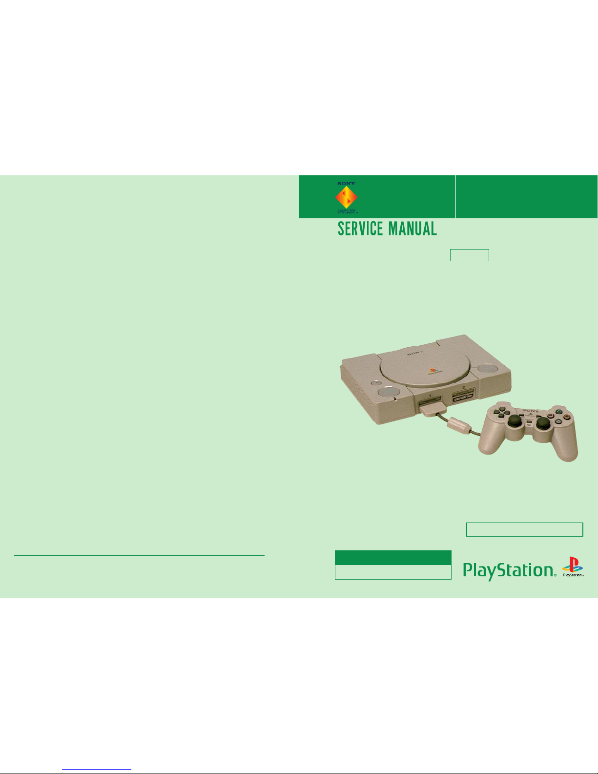
SECTION 2
EXPLODED VIEW
The components identified by
mark ! or dotted line with mark.
! are critical for safety.
Replace only with part number
specified.
CAUTION
CAUTION :
Use of controls or adjustments or performance
of procedures other than those specified herein
may result in hazardous radiation exposure.
— 4 —
SCPH-9000 SERIES
Reproduction Prohibited
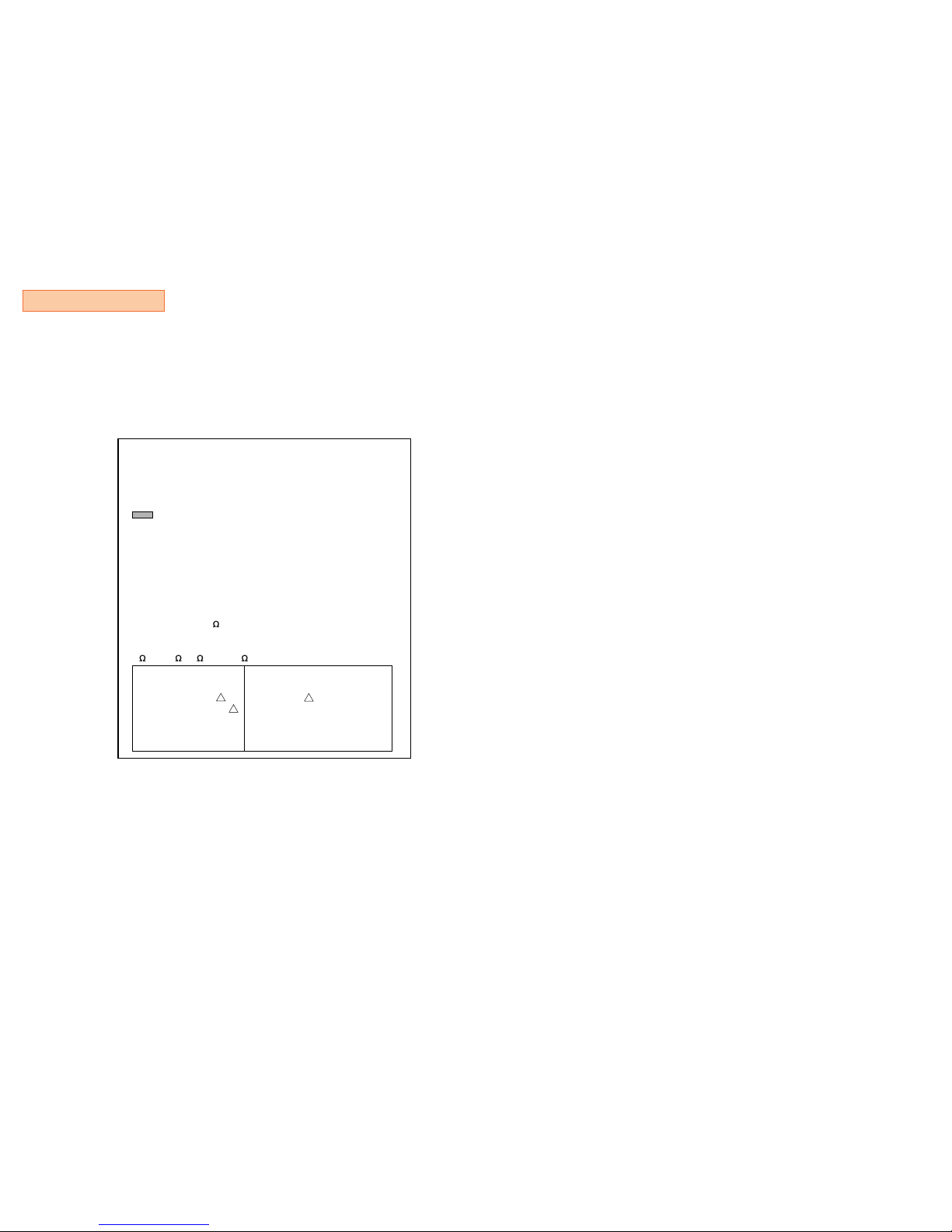
3-1. Test Specification
RF Level 0.90 to 1.35 Vp-p (Test point : Between CL704 and CL710)
Use SCD-2700 DISC when measured RF level.
Use an oscilloscope with input impedance over 10 M Ω
RF Jitter Less 9.0 nS (Measuring with KSM- 6135S JITTER METER.)
Less 27.0 nS (Measuring with KSM- 6235S JITTER METER.)
PP Level 1.1 ±0.6 Vp-p (Test point : Between CL776 and CL710)
Use LPF (fc = 10 kHz)
Tracking Level 1.3 ±0.6 Vp-p (Test point : Between CL709 and CL710 )
Caution Vc Line (CL710) do not wire to other lines together.
Caution. Vc Line (CL710) do not make common use with GND line.
Test Point for PU-23 Board.
1-674-987-
52
1
14
15
14
59
13 15
53
R747
R775
R770
R793
R750
R732
R733
FB703
C742
C720
C726
C721
L701
C701
R723
CL760
CL708
CL706
CL780CL778
CL777
CL776
CL790
C741
CL791
CL711
CL709
CL728
CL786
CL784
CL787
CL785
CN701
FB701
FB704
CL775
CL710
Q701
CL316
CL704
CL727
C729
C725
C718
C761
C716
C738
C739
HA002
R727
FB702
R717
CL779
11 12
1-674-987-
CL776
CL727
CL709
CL710
CL704
CL706
CL728
SECTION 3
ADJUSTMENT
• RF signal waveform (Eye pattern)
0 V
VOLT/DIV
TIME/DIV
0.90 to 1.35 Vp-p
: 0.2 V
: 500 nS
SECTION 4
NOTICE
Circuit Notes :
: B+ Line.
Voltages are measured with a Digital Multimeter. (Input impedance over 10 MΩ.)
Waveforms easured with an Oscilloscope DC coupled.
Semiconductors.
In each case. u : µ, for example ; uA : µA, uPA : µPA, uPB : µPA, uPC : µPA.
Unit Descriptions :
Capacitors.
Unit of Capacitor is µF and pF, for example ; uF : µF, pF : µµF.
Resisters.
Unit of Resistor is Ω.
Inductance.
Unit of Inductance is µH and mH
Parts List Notes:
Due to standardization, Parts may be different from the parts described in the diagrams or used on
the Set.
Attention :
Dielectric voltage withstand test and Insuiation resistance test.
After repair complete. Dielectric voltage withstand test and Insulation resistance test to be conducted according to the regulation of IEC-65 EN60065 or UL1492 or .
About replacement of Optical Device.
Before exchanging the Optical Device, Check the RF level, Jitter, Eye pattern, Focus gain and
Tracking error. When Optical Device is meet the specification, Playback the PS1 testing disc
“QA-DISC” or “AGING DISC” for checking the double speed and sled mechanism ability.
Optical Device should have to no exchange when spacification and ability are satisfied.
— 5 —
SCPH-9000 SERIES
Reproduction Prohibited
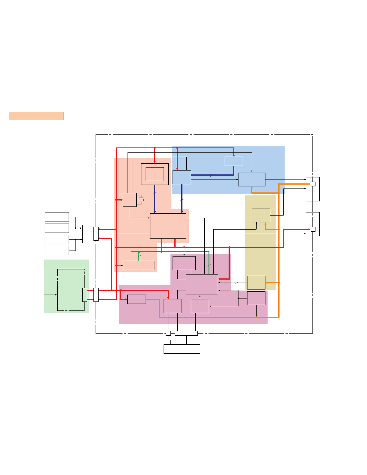
SECTION 5
BLOCK DIAGRAMS
POWER
AUDIO
VIDEO
CPU
SERVO
IC722
(DRIVER)
BA5977
IC304
(SUB CPU)
MC68HC05G6
IC723
(CD, RF)
CXA2575
IC201
(SG-RAM)
IC502
VDAC +RGB
(
ENCODER
)
IC102
(BOOT RAM)
IC602
(RIPPLE)
LP2985
IC310
4Mbit
DRAM
Filter
SER +3.3V
DIG +5V
MAIN BUS
X201
5V
MOT +8V
SUB BUS
4.19MHz
33.8688MHz
VIDEO OUT
AUDIO OUT
67.7376MHz
NTSC : 53.693175MHz
PAL : 53.203425MHz
NTSC : 3.58MHz
PAL : 4.43MHz
AUD +5V
CN701 CN702
CN602
+8V
+3.5V
AC IN
+3.3V
CONTROLLER
MEMORY
CARD
TERMINAL
BOARD
FRONT
CONTROLLER
IC204
IC732
(CD-ROM
CONTROLLER
+ CD DSP)
CXD2938
OPTICAL DEVICE
KSM-440AEM
IC103
(CPU)
CXD8606
IC601
78M05
CN102
CTR3.3V
PU-23 BOARD
POWER
SUPPLY
BLOCK
EXT +8V
IC405
(DAC)
NJM2174
IC203
(GPU)
CXD8561
VID +5V
CN502
AV MULTI OUT
CN104
SERIAL I/O
MEMORY
CARD
32
32
32
16
16
8
IC106
(DRAM)
16Mbit
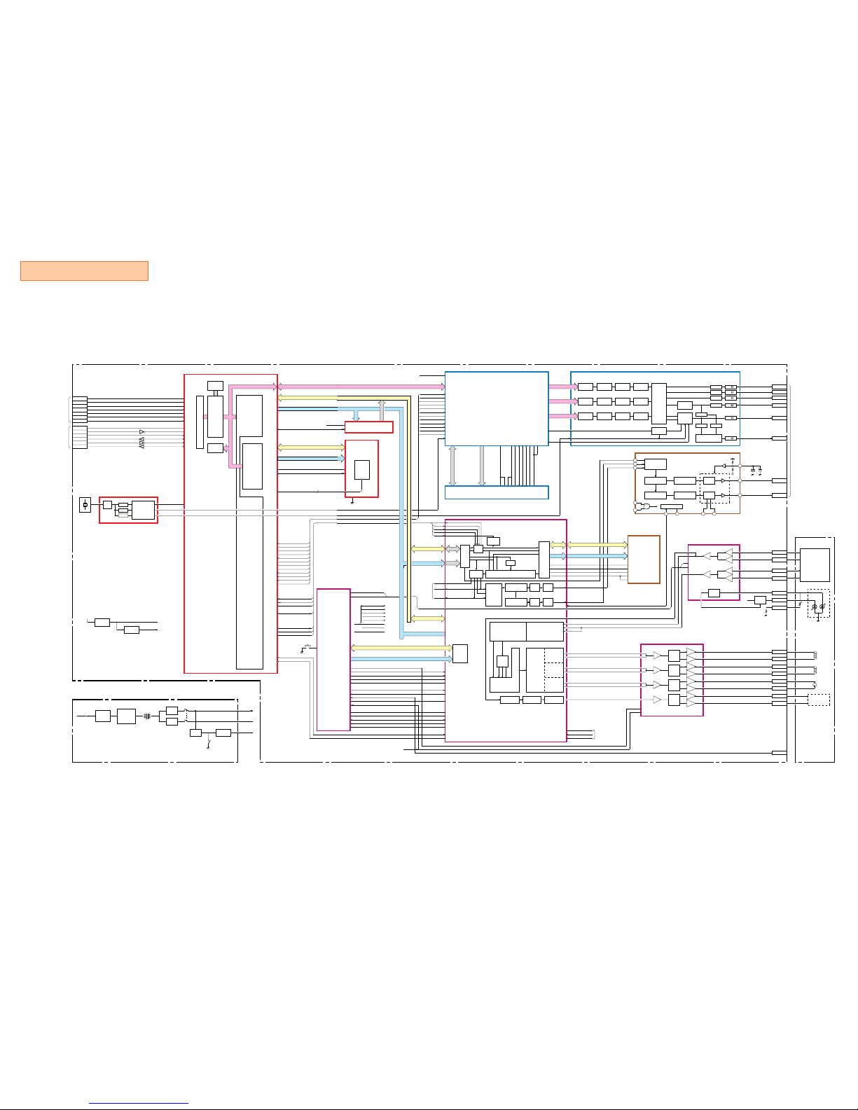
— 6 —
SCPH-9000 SERIES
Reproduction Prohibited
RES3.3
127
128
126
125
124
122
123
131
134
DQM1
DQM3
DQM0
DQM2
WE
CAS
RAS
CS
DSF
CLK
565723242526272853
55
DQMH
DQMLWECAS
RAS
MCS0
DSF
MCLKOUT
MCLKIN
MUTO
AOUTL
AOUTR
154
147
150
105
6
24-28, 31-36, 39-42,
45-50, 53-59, 62-65
SR0-SR7
77-79, 82-86
89-95, 98-104
107-112, 115-118
RST
137-140
143-145
148-150
29, 31-34
47-51
1, 3, 4, 6, 7, 9, 10,
12, 13, 17, 18, 20,
21, 60, 61, 63, 64,
68, 69, 71, 72, 74,
75, 77, 78, 80, 81,
83, 84
D0-D31
GPU
FD0-FD31 LA0-LA9
DQ0-DQ31 A0-A9
IC203
VIDEO DAC + RGB ENCODER
IC502
IC201
SG RAM
SD0-SD15
1, 2, 5-14
16-19
20-27, 30
R
DECODER
R
SG0-SG7
G
DECODER
G
SB0-SB7
C SYNC
NTPL
SPMUTE
AU-R
AU-L
SPMUTE
RESET
B
DECODER
CELL
MATRIX
CELL
MATRIX
CELL
MATRIX
BURST
FLAG
Y/C
M/X
CHROMA
GEN.
SYNC
ADD
LATCH
LATCH
LATCH
SCF
APC
SCF
CLOCK DIVIDER
CLAMP
CLAMP
MATRIX
CLAMPB
HD0-HD15
HA1-HA8
IC732
SD0-SD15
125-142
105,107-111,113-116
85-92
97-99,101,102
HD0-HD15
DTIB
BCK0
LRC0
CD-ROM CONTROLLER + CD DSP
4Mbit DRAM
IC310
CD-RF
PDIC
KSM440AEM
IC723
14
15
13
SYNC IN
SC IN
NT/PAL
B-Y
R-Y
Y
B
G
R
156
157
181
179
182
178
OE
WE
RAS
UCAS
LCAS
27
57
55
53
54
58
59
11
12
13
14
17
18
15
16
122
SPEED
RESET
6
7
5
4
22
23
2
3
20
37
38
39
RFAC
TFDR
TRDR
FRDR
FFDR
SRDR
SFDR
SRD
SWR0
SYSCLK1
FE
SE
XOE
XWE
XRAS
XCAS
119
120
144
XHRD
XHWR
SYSCK
27
13
14
28
29
LPF
BPF Y TRAP
6dB 75
75
75
6dB 75
6dB 75
6dB 75
MD0-MD15
2-5, 7-10
31-34, 36-39
16-19, 22-26
160-164, 166-172
174-177
MA1-MA9
MED0-MED15
MEA0-MEA8
183-186, 188-192
I/O 1-16
7
6
PD1
PD2
5
4
E
F
MI
LD
TRK–
TRK+
FCS–
FCS+
SL–
SL+
SP–
SP+
SLED
MOTOR
FOCUS
COIL
TRACKING
COIL
8
A0-A8
HA0-HA9
SA0-SA9
SUB CPU
I/F
CLV
PROTECTOR
LEVEL
SHIFT
IC722
DRIVER
LEVEL
SHIFT
LEVEL
SHIFT
LEVEL
SHIFT
SWITCH
AND
BUFFER
MIRR
DFCT
FOK
SERVO DSP
TRACKING
PWM
GENERATOR
TRACKING
PWM
GENERATOR
TRACKING
PWM
GENERATOR
TIMING
GENERATOR
PWM
GENERATOR
A/D
CONVERTER
SYNC
PROTECTOR
5
6 7
SPCLK
19 18
12
13
2
VREFL
VOOM
M_R
TRM_L
TRM_R
+5V
IC405
7
4
5
11
REG
Q701
SERIAL INPUT
INTERFACE
8x
INTERPOLATOR
XLT1
8x
INTERPOLATOR
∆
∑
MODULATOR
∆
∑
MODULATOR
502-2
LD
702-12
M_G
502-1
M_B
502-4
M_Y
502-8
M_C
502-6
M_VIDEO
502-7
M_AUL
502-11
M_AUR
+B
9
502-9
702-7
702-6
702-8
702-4
702-9
702-1
702-10
702-15
702-14
702-16
702-13
701-1
701-2
701-4
701-3
AMP
AMP
AMP
AMP
AMP
AMP
AMP
BUFF
BUFF
BUFF
BUFF
BUFF
BUFF
BUFF
BUFF
AMP
AMP
AMP
SPINDLE
MOTOR
BLOCK
M
LASER DIODE
13
2
14
199
17
12
9
5
4
3
1
206
192
15
13
11
12
16
IREQ
A2
H BLANK
PCK
V BLANK
DREQ
SYSCLK
DACK
WR
RD
CS
D SYSCK
VCKN-A
GPUNIT
GPUA2
H BLANK
PCK
V BLANK
GPUDREQ
SYSCLK0
GPUDACK
GPUWR
GPURD
GPUCS
DBLCLK
RES3.3
36
35
34
32
33
31
41
96
DREQ
XIRQ
DACK
XRD
XWR
XCS
SYSCLK1
DTIB
SPUDREQ
SPUNIT
SPUDACK
SRD
SWR0
SPUCS
SYSCLK1
EXTDATA
74
75
76
77
80
81
11
94
95
96
79
82
103
117
DATA
XLAT
CLOK
SCOR
SQCK
SQS0
FSOF
XCS
XWR
XRD
XINT
SENS
XHCS
H INT
SPUDREQ
SRD
SWR0
SPUDACK
SYSCLK1
SA1-SA9
AV MULTI OUT
24
22
23, 25-31
1-12
13-15,
17-21
OE
CE
BOOT RAM
IC102
SRD
44
27
2-5, 7-10,13-16,18-21
50-53,55-58,61-64,66-69
28-34, 37-39
WE
RAS
I/O1-I/O32
A0-A9
33-38, 40, 41
6-10
SUB CPU
IC304
S301
DECD0-DECD7
19
DECA0-DECA4
DOOR
SPEED
DAT0
XLT0
CLK0
SCOR
SQCK
SUB Q
LS
MCLK
XRST
MCS
MWR
MRD
MINT
SENS
CD RD CS
CD RD INT
27
43
44
45
31
26
24
18
14
13
46
47
48
30
23
SPEED
DATA
XLT
CLK
SCOR
SQCK
SUB Q
LMTSW
DSC1
RESET
DECCS
DECWR
DECRD
X INT
SENSE
LDON
AGC_CNT
49
28
LDON
MIRROR
OE
45-48
HYPER DRAM (16M)
IC106
IC106
CAS1-4
A0-A19 D0-D7
MCA0-MCA4MCA0-MCA4
MCD0-MCD7MCD0-MCD7
FROM IC103
DMA
TIMING
GEN
HOST
IF
ENV
SERIAL
IF
DSP
8x
INTERPOLATOR
8x
INTERPOLATOR
SERIAL
INPUT
INTERFACE
EXRAM
IF
∆
∑
MOD
SCF
∆
∑
MOD
SCF
FROM IC103
81
83
84
80
77
82
89
SCK0
TXD
RXD
DTR0A
DTR0B
DSR
INT
102-10
102-8
102-6
102-5
102-3
102-2
102-1
75
73
74
71
72
70
VD0-VD31
SD0-SD15
SA0-SA23
CS2
RXD
DSR
TXD
CTS
DTR
RTS
5 67MHz
6
3.58MHz (NTSC)
4.43MHz (PAL)
1
53.63MHz (NTSC)
53.20MHz (PAL)
SCK0
TXD0
RXD0
DTR0A
DTR0B
DSR0
INTIN10
SIO
161-165, 172-181, 184-194, 197, 198
MAIN DATA BUS (GPUD0-GPUD31)
RXD1
DSR1
TXD
CTS1
DTR1
RTS1
97
43, 4
CRYSTALP
Q106 (1/2)
Q106 (1/2)
Q105 (1/2)
Q105 (1/2)
104-1
104-3
104-4
104-5
104-6
104-8
CONTROLLER
SERIAL I/O
CPU
IC103
EP ROM
CONFIGURABLE
MULTIPLEXER
AND
DIVIDE LOGIC
DWE
DRAS0
DCAS0-DCAS3
43
45
46-49
DD0-DD31
5-13, 16-25,
28-37, 40-42
DA0-DA7
DA9
DA11
55, 57, 59-64
67, 68
107-116, 119-142
145-152, 132-142, 125-129
PLL 1
IC204
X201
14.318182MHz (NTSC)
17.37MHz (PAL)
REF.
OSC
PLL 2
PLL 3
4
SYSTEM
RESET
DC-AC
CONV.
SWITCHING
REG.
ADDRESS BUS (SA0-SA23)
SUB DATA BUS (SD0-SD15)
SRD
SWR0
SYSCLK1
101
100
154
RES3.3
SRD
SWR0
SYSCLK1
95
94
CS5
INT IN2
88
90
87
96
SPUDREQ
SPUNIT
SPUDACK
SPUCS
DREQ4
INT IN9
DACK4
CS4
102
153
159
160
199
200
201
202
203
204
205
206
GPUNIT
GPUA2
H BLANK
PCK
V BLANK
GPUDREQ
SYSCLK0
GPUDACK
GPUWR
GPURD
GPUCS
DBLCLK
INT IN1
VA2
TCLK1
TCCK0
INT IN0
DREQ2
SYSCLK0
DACK2
VWR
VRD
CS7
DSYSCLK
+5V
REG.
+8V
+3.5V
REG.
+5V
SER +3.5V
RECT.
RECT.
FULL
WAVE
RECT.
UC
AUS/UK/AEP
POWER SUPPLY BLOCK
PU-23 BOARD
2A/125V
1.6A/250V
F001
RECT.
+8V
+3.5V
MDEC
CPU CORE
B/U
DRAM
CONTROLLER
GTE
— 7 —
SCPH-9000 SERIES
Reproduction Prohibited
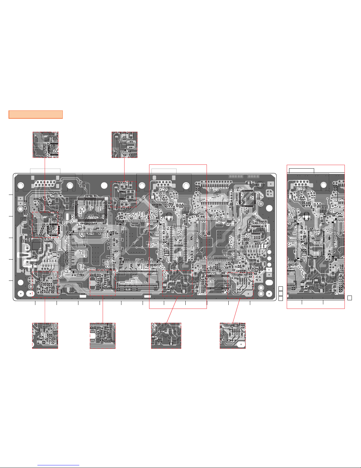
SECTION 6
PRINTED WIRING BOARDS AND SCHEMATIC DIAGRAMS
THIS NOTE IS COMMON FOR PRINTED WIRING
BOARDS AND SCHEMATIC DIAGRAMS.
Note on Printed Wiring Boards :
••Through hole is omitted.
: Pattern on the side which is seen.
Note on Schematic Diagram :
•
•
•
•
Use caution when replacing chip parts.
New parts must be attached after removal of chip.
Be careful not to heat the minus side of tantalum capacitor,
because it is damaged by the heat.
All capacitors are in µF unless otherwise noted. pF : µµF 50 WV
or less are not indicated except for electrolytics and tantalums.
All resistors are in and 1/4 W (Chip resisters : 1/10w) unless
otherwise specified.
Chip resistors are 1/8 W or 1/10 W unless otherwise noted.
k : 1000 , M : 1000 k .
Note :
The components
identified by mark
!
or
dotted line with mark
!
are critical for safety.
Replace only with part
number specified.
Note :
Les composants identifies par
une marque ! sont critiques
pour la securite.
Ne les remplacer que par une
piece portant le nubero specifie.
— 8 —
SCPH-9000 SERIES
Reproduction Prohibited
A
B
C
D
E
F
123456
7 8 9 10 11 12
IC201
IC405
IC203
IC204
IC106
IC103
IC310
IC602
IC102
IC732
IC722
IC304
IC723
IC502
IC601
208
1
148
5
1
52
53104
105
156
157
1
35
36
13
45
70
208
52
1
152
1
1
14
1528
114
59
13
2
610 16
15
10
1120
53
104
105156
157
20
21
40
208
104
116
1732
105
156
157
1
2
9
10
1357
2468
31
50
51
80
81
100
1
17
14 8
30
1
1
1
5
3
2
12
13 24
25
36
3748
1
CN502
C635
D510
D511
C524
C631
C511
C510
R541
R542
R215
C622
R606
CL505
CL508
CL507
CL512
CL510
CL613
Q505
CL506
FB502
C508
C602
C519
C523
C642
C606
PS603
PS601
L104
FB201 FB202
C639
FB123
R150
R142
R132
R133
D103
D101
FB121
FB122
FB120
FB117
ET102
C209
C116
C115
C114
C118
C122
C641
C611
C137
C108
C109
RB123
RB119
ET101
R135
R154
C702
R619
C744
R734
R739
R738
R741
R796
R745
R746
R747
R775
R770
R793
R750
R732
R733
FB703
C742
C720
C726
L701
R748
R749
R783
FB710
C740
C701
C728
C743
C737
C763
C762
C736
R345 R344
C150
C326
C306
RB122
S301
C129
C130
L606
FB602
C617
C317
C637
C705
C745
C714
R706
R774
R723
R704
R705
C703
C706
C776
C146
C113
C238
C104
C134
C213
C215 C217
C112
C218
C138
C111
C110
FB111
FB114
FB112
C223
C445
C407
C409
R107
FB102
R207
R205
JR201
RB125
JR202
L203
X201
FB119
FB118
CN602
C620
C621
C523
C245
C239
C220
C228
R528
R527
R529
C502
C509
FB504
FB503
FB401
FB402
D503
C551
C550
C227
C243
C225
C244
C236
C241
C222
C529
C145
R425 R429
L401
C247
C242
CL511
CL101
CL401
CL534
CL129
CL162
CL128
CL163
CL132
C144
C208
C221
C224 C226
C530
C424
C404
C406
C423
C408
R430 R426
CL502
CL501
CL503
CL608
CL509
CL603
PS604
L604
R522
R521
R520
R518
R517
C608
C609
L507
R501
C627
C601
C607
CL611
CL605
CL118
CL606
CL152
CL131
CL119
CL199
L106
CL105
CL137
R140
R139
R141
R137
R138
CL150
CL151
C214
C216
C248
C249
CL601
CL205
CL206
L601
C605
C240
C211
C210
C219
C136
C106
C105
C234
C235
R204
R206
CL117
CL607
CL134
CL136
CL103
CL104
CL138
CL102
CL166
CL705
CL133
CL167
CL111
CL526
CN104
FB115
FB113
FB116
CL527
CL528
CL529
CL531
CL532
CL160
CL115
C102
C151
C140
CL120
CL124
CL126
CL161
CL143
CL121
CL110
CL144
CL145
CL112
CL147
CL146
CL113
CL155
CL107
CL140
CL106
CL114
C319
R342
R341
R341
C325
L304
CL315
CL154
CL159
CL149
CL127
CL125 CL122 CL157 CL123
CL158 CL156 CL130 CL109
CL142 CL141
CL108
CL530
L102
CL533
CL164
CL614
CL795
CL762
C768
CL794
CL793
CL774
CL792
CL796
CL761
CL719
CL760
CL769
CL773
CL782
CL781
CL783
CL708
CL706
CL780CL778
CL777
CL776
CL790
C741
CL791
CL711
CL709
CL728
CL786
CL784
CL787
CL785
CN701
FB701
FB704
CL775
CL779
CL710
Q701
CL316
CN702
C774
R795
R769
R740
CL704
CL727
CL799
CL610
L607
C731
R702
R703
R701
R725
C704
C747
C733
C724
C709
C715
C729
C725
C761
C738
C739
HA002
R727
R712
R714
C749
FB702
R717
R710
C327C315
C132
C131
C133
C316
C773
C775
C767
C124
C139
C101
RB120
RB124
R104
R134
R338
Q106
Q105
R136
R904
R901 R903R902
R148
R146
D104
RB121
JR203
R620
R115
CL201
CL116
PS602
CN102
PS605
CL612
R519
CL604
CL504
11
12
2
113
14
26
27 39
40
52
1-674-987- 31
21
11
PU-23 BOARD (-11/-21/-31/-41/-51)
8 97
1-674-987- 41
IC310
IC602
35
36
13
45
52
1
1
28
1
156
157
20
21
40
208
104
1
32
105
1357
2468
C118
C122
C641
C611
C137
C108
C109
RB123
RB119
ET101
R154
C702
R619
RB122
S301
C129
C130
L606
FB602
C617
C317
C637
C705
C745
R706
R704
R705
C703
C706
C776
FB111
FB114
FB112
CL607
CL134
CL136
CL103
CL104
CL138
CL102
CL166
CL705
CL133
CL167
CL111
CL526
CN104
FB115
FB113
FB116
CL527
CL528
CL529
CL530CL532
CL531
CL160
CL115
C102
C151
C140
CL120
CL124
CL126
CL161
CL143
CL154
CL159
CL149
CL127
CL125
CL158
L102
CL533
CL164
CL614
CL795
CL762
C768
CL794
CL793
CL774
CL792
CL796
CL761
CL799
CL610
L607
C731
R702
R703
R701
R725
C704
C733
C724
C327
C315
C132
C131
C133
C315
C775
C767
C124
C139
C101
RB120
RB124
R134
R135
R338
Q106
Q105
R136
R148
R146
D104
RB121
Note : PU-23 board number suffix of -41 is described partially.
IC502
1
12
13 2
4
3748
C511
C510
R54
C
C508
C5
C523
3
R528
C502
C509
CL608
CL509
L604
R501R502
C608
C609
R543
IC405
17
14 8
C407
C409
L401
47
5
34
C530
C424
C404
C406
C423
C408
R430 R426
R423
C639
FB123
R150
R132
R133
D103
D101
FB120
FB117
FB118
CL199
L106
CL105
CL137
R140
R137
R138
CL150
L
CL116
IC204
148
5
208
C209
R205
JR201
JR202
L203
X201
C210
C219
C234
C235
R204
R206
JR203
R620
CL201
IC602
13
45
C641
C617
L606
FB602
C
C637
CL607
CL614
CL610
L607
C618
14
15
14
R775
R
R
FB703
C
C
CL
7
CL784
CL787
CL785
CN701
FB701
CL727
C725
C718
R727
Suffix of -51 Suffix of -51
Suffix of -51 Suffix of -51 Suffix of -51 Suffix of -51
 Loading...