


EL4737HB and EL4737HB-ICE

 320 x 128 Pixel Electroluminescent Display
Product Profile |
OperationsManual |
|
|
The EL4737HB and the EL4737HB-ICE displays are low power, rugged, high-resolution electroluminescent (TFEL) flat panel displays. They replace the LCD or bulky CRT in instrument product designs. Their compact dimensions save space that can allow addition of features or reductions in overall size. They are designed to function in extreme environments, and the crisp displays are viewable under most lighting conditions at wide viewing angles. Their ease of installation reduces system integration costs.
The EL4737HB and the EL4737HB-ICE are 320 column by 128 row flat panel displays. The pixel aspect ratio is 1:1. The CRT-type interface is TTL-compatible and is designed to match the needs of most systems. These displays also have an interface mode for hardware compatibility with the Hitachi HD61830B or equivalent LCD controller. These displays may be driven at frame rates up to 120 Hz for applications requiring extra brightness.
The displays require DC power and four basic signals to operate:
1.Video Data or pixel information (VID)
2.Video Clock, pixel clock, or dot clock (VCLK)
3.Horizontal Sync (HS)
4.Vertical Sync (VS)
EL Technology
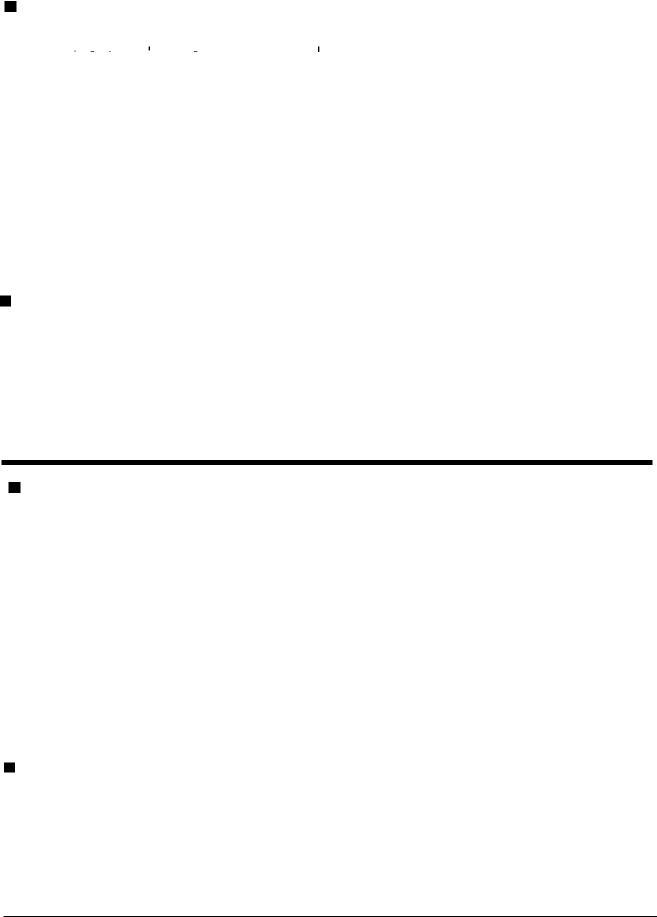
A display consists of an electroluminescent glass panel and a mounted circuit board with control electronics.
ALUMINUM ROW
ELECTRODE
DIELECTRIC
LAYERS
1 micron |
|
LIGHT EMITTING LAYER |
|
|
|
|
||||||
1 mm |
|
|
|
|
|
|
|
|
|
|
|
|
|
|
|
|
|
|
|
|
|
|
|
||
|
|
|
|
|
GLASS |
SUBSTRATE |
||||||
|
|
|
|
|
|
|
|
|
|
|
|
|
|
|
|
TRANSPARENT |
|
|
VIEW |
||||||
|
|
COLUMN ELECTRODE |
|
|
|
|
||||||
The EL glass panel is a solid-state device with a thin film luminescent layer sandwiched between transparent dielectric layers and a matrix of row and column electrodes. The row electrodes, in back, are aluminum; the column electrodes, in front, are transparent. The entire thin film device is deposited on a single glass substrate. A circuit board is connected to the back of the glass substrate. Components are mounted on this circuit board within the same area as the electroluminescent viewing area on the glass panel. The circuit board is connected to the glass with metal-on-elastomer interconnect technology. The result is a flat, compact, reliable and rugged display device.
The EL4737HB-ICE display includes a light absorbing Integral Contrast Enhancement (ICETM) construction of the display glass. ICETM background
significantly improves the luminance contrast of the display in bright ambients, and makes the display easier to read by increasing the crispness of the pixels.
The 320 column electrodes and 128 row electrodes are arranged in an X-Y formation with the intersecting areas performing as pixels. Voltage is applied
V(t) to both the correct row electrode and the correct column electrode to cause a
lit pixel. Special operating voltages required are provided by a DC/DC converter.
®
T he Definition of Quality ®

EL4737HB, EL4737HB -ICE |
2 |
Electrical Characteristics
Display
The EL4737HB and EL4737HB-ICE products consist of a display, a DC/DC converter, and interconnecting cable as shown below.
|
|
BackofDisplay |
|
J1 |
|
|
|
J1 |
|
|
|
|
P3 |
DC/DCConverter |
|
1 |
2 |
2 |
16 |
P1 |
J3 |
||
|
|
|
|
|
J0 |
|
|
J1 |
|
1 |
15 |
|
|
P0 |
J0 |
19 |
20 |
|
|
Input to the Display at P0
Pins |
Signal |
Symbol |
Description |
1, 2 |
Voltage |
VH |
+12V. See also the descriptions of DC power requirements on page 4. |
3, 4 |
Voltage |
VL |
+5V optional input, see page 4. |
5 |
Scan Mode |
SMODE |
Mode 1 (Standard timing) is selected by taking pin 5 high (or left unconnected). Mode 2 (LCD |
|
|
|
timing) is selected by pulling pin 5 low. This signal passes directly from the user to the display |
|
|
|
via the DC/DC converter. It is not buffered or terminated within the DC/DC converter. |
6not connected
7, 8, 10 |
|
|
|
|
12, 14, 16 |
Ground |
GND |
Signal return. |
|
9 |
Vertical Sync |
VS |
A new frame is initiated by the high state of VS. To properly sync the EL display, VS must be high |
|
|
|
|
at the end of line 1. This signal passes directly from the user to the display via the DC/DC |
|
|
|
|
converter. It is not buffered or terminated within the DC/DC converter. |
|
11 |
Horizontal Sync |
HS |
Mode 1: HS high time brackets the active pixel data for a horizontal scan line. Mode 2: HS marks |
|
|
|
|
the last pixel of a horizontal scan line. HS high time should be less than 1 tVCLK. In either mode, |
|
|
|
|
HS period must be an even multiple of 4 tVCLK. The last 320 pixels prior to the falling edge |
|
|
|
|
of HS will be visible on the display. This signal passes directly from the video source to the display |
|
|
|
|
via the DC/DC converter. It is not buffered or terminated within the DC/DC converter. |
|
13 |
Video Clock |
VCLK |
VCLK provides the necessary signal to latch in the information present on VID. The VID and HS |
|
|
|
|
signals are referenced to VCLK, which must continuously run. Data latching occurs on the falling |
|
|
|
|
edge of VCLK. This signal passes directly from the video source to the display via the DC/DC |
|
|
|
|
converter. It is not buffered or terminated within the DC/DC converter. |
|
15 |
Video Data |
VID |
VID contains the serial video data to be displayed. A logic high corresponds to a lit pixel. Pixel |
|
|
|
|
information on VID is supplied from left to right and from top to bottom; the first bit of data on |
|
|
|
|
VID at the beginning of a frameis displayed as the pixel at the upper left corner of the display. |
|
|
|
|
Bit number 320 is at the upper right corner. Bit number 321 is directly beneath pixel number |
|
|
|
|
1 and so on. This signal passes directly from the video source to the display via the DC/DC |
|
|
|
|
converter. It is not buffered or terminated within the DC/DC converter. |
|
|
|
|
|
|
3 |
EL4737HB, EL4737HB-ICE |
VideoTimingatP0
StandardVideoTiming(Mode1)
Mode1VideoParameters
Parameter (Symbol) |
|
Min. |
Max. |
Units |
|
1 |
Videoclockperiod |
(tVCLK) |
195 |
— |
ns |
2 |
VCLKrise/falltime |
(tDR/tDF) |
— |
15 |
ns |
3 |
VCLKlowtime |
(tWL) |
100 |
— |
ns |
|
VCLKhightime |
(tWH) |
100 |
— |
ns |
4 |
VIDsetuptoVCLK |
(tDS) |
50 |
— |
ns |
5 |
VIDholdfromVCLK |
(tDH) |
50 |
— |
ns |
6 |
HSholdfromVCLK |
(tHSH) |
50 |
— |
ns |
7 |
HSsetuptoVCLKfall |
(tHSS) |
50 |
— |
ns |
|
|
|
|
|
|
320
Parameter (Symbol) |
|
Min. |
Max. |
Units |
|
|
|
|
|
8 HSlowtime1 |
(tHSlow) |
8 |
— |
tVCLK |
9 HShightime |
(tHShigh) |
320 |
— |
tVCLK |
10VSholdfromHS |
(tVSD) |
0 |
— |
ns |
11VSsetuptoHS |
(tHSD) |
60 |
— |
ns |
12VShigh/lowwidth |
(tVSh/l) |
1 |
— |
tVCLK |
13HSperiod1 |
(tHS) |
65 |
— |
µs |
14VSperiod |
(tVS) |
128 |
— |
tHS |
FrameRate |
(1/VSperiod) |
— |
120 |
Hz |
1 VCLKmustberunningduringHSlowtime.
VideoTimingatP0 forHitachi61830BLCDController(Mode
319 320
Mode2VideoParameters
Parameter (Symbol) |
|
Min. |
Max. Units |
||
1 |
Video clock (CL2) period |
(tVCLK) |
195 |
630 |
ns |
|
VCLK rise/fall time |
tDR/tDF |
— |
15 |
ns |
2 |
VCLK lowtime |
(tWL) |
100 |
— |
ns |
|
VCLK high time |
(tWH) |
100 |
— |
ns |
3 |
VID setup to VCLK |
(tDS) |
50 |
— |
ns |
4 VID hold from VCLK |
(tDH) |
50 |
— |
ns |
|
5 |
HS (CL1) high time |
(tHShigh) 100 |
tVCLK |
ns |
|
|
|
|
|
|
|
|
Parameter (Symbol) |
|
Min. |
Max. |
Units |
|
|
6 |
HS setup time |
(tHSS) |
100 |
tWL |
ns |
|
|
7 |
HS hold from VCLK |
(tHSH) |
0 |
tWH |
ns |
|
|
8 |
VS (FLM) setup to HS |
(tHSD) |
400 |
— |
ns |
|
|
9 |
VS hold from HS |
(tVSD) |
1000 |
— |
ns |
|
|
|
|
HS (CL1) period |
(tHS) |
320 |
— |
tVCLK |
|
|
|
VS period |
|
(tVS) |
128 |
— tHS |
|
|
|
FrameRate |
(1/VS period)— |
120 |
Hz |
|
|
|
|
|
|
|
|
|
|
 Loading...