

Page 1
proNeerl"
(v)
Tlp
Art
ot Entertaiment
6
^
Service
_EB
q
_f__l:i
io
:tr)lo6a-
/oo.
Manual
STEREO
MULTI-PLAY
CD
CASSETTE
R.P7
r;
o6tb
.68
it
a5
DECK
RECEIVER
4()M
ORDER NO.
RRV1O23
-P64olul
x
x
STEREO
XR
XR
XR
R
R
-P34()M
CD
I
I
I
CASSETTE
P
P
P
7
6
3
4
4
4
DECK
o
o
o
RECEIVER
r
THIS
MANUAL
Typ.
SD
KU
KC
xR-P740M
o
o
IS
APPLICABLE
xR-P740
o
xR-P640M
o
o
TO
THE FOLLOWING
Modol
XR-P6/|{)
o
CONTENTS
CHAPTER
PIONEER
PIONEER
PDNEERELECTROI{ICSOFCANAOA,tNC.3O0A
PIONEER
PIoNEEB
o P|oNEER
1
ELECTRONIC
ELECTRONICS
ELECTROT{IC
ELEcrRoNlcs
ELECTRONTC
SERVTCE lNC.
[EUROPE]
AusrBALla Pw.
CORPORATION
pO
Box 1760,
N.V Haven
CORPORATTON
jO87
LTD. r78 r84
IVIODEL(SI
xR-P3/l(,M
o
o o
o
o
-5
-8
-9
-tl
-20
4,j, Mesuro
Long
slareparkwayN.4arkham,OntanoL3BOp2Canada
Keetberataan
Bea;h, CatrJornra
Boundary
1993.
xR'P340
o
1.8 PARTS
EXPLODED
1.9
PCB PARTS
CHAPTER
2.1
PACKING
2.2
SCHEMATIC
DfAGRAMS
I chome, Mesuro
t,9j2O Met;ete.
ioad
90801 U.S.A.
B aesroe. vr.fo.ra
Betorurn
AND TYPE(S}.
Powor
Roquhemant
AC110V
AC240V
AC120V
AC120V
t120-
220V
t240V
LIST
2
AND EXPLODED
ku, rokyo 1s3
3195
127V
FOR PACKING
VTEWS
LIST
AND
Japan
Ausrra a TLL
r DFF
Tha vohago
by lh. folowlng
I
With the
... .......
PCB CONNECTION
[03]
DEC. 1993
cln ba
convanod
m.thod.
voltago solector
AND
..............
...
VIEWS
580,99r1
, .
.........2-16
Printed
1 - 38
1-47
2-2
in
Japan
Page 2
XR-P74()M,
xR-P7
&, XR-pOaO,
XR-P64()M,
XR-P34()
XR-P34()M
CHAPTER
1.1
SAFETY INFORMATION
This
service manual
1
is
do-it-yourselfer. Oualified
trained to
lmproperly
properly
performed
the warranty,
risk trying
not
WARNING
Lead in 3oldor
may
cause birth
Whsn s.rvicing
the
3oldor. Alao,
NOTICE
(FOR
CANADIAN
Fuse
symbols
must
be ol adentical designation.
REMARQUE
(POUR
Les symboles
pidces
de remDlacement
us6d
o. handling
MODELE
de lusible
and safely repair
repairs
you
It
defoct.
when aold.rlng do not inhala
€S
are not
to
do so
and reter the repair to
ptoducl
in thlr
or othor r.prcductive hetm
circuit board. end
MODEL
CANADIEN
ONLY)
(last
operating fuse) and/or
SEULEMENT)
€F
doivent avoir la mCme
intended for
technicians
quallfled
have
complex
can
adversely
qualified
ir liltod by th. Celifornia
(fusible
pertorm
to
(Calllo.nia
oth.. compon.ht!
eny amok.
de type rapide) evou
d€sionation.
service technicians;
the necessary
products
aftoct
ths repair
qualllled
a
or lurnar
€*
such as those
ths.satety
ot
servlce techniclan.
Hcalth
and Wcltaro agoncy
Hoelth
& Saf.ty Cod., Sectlon
which contein l..d in
produc.d.
(slow
operating fuse) on PCB indicate
-E8-
lt ls not
test
equiprnent and tools,
covered by this
and retiability
product
thls
(tusible
of the
properly
aa a known .sproductiva
25249.S).
.old.r, .void unprotoctod
de type lent)
meant tor the
casual
and have
manual.
product
and
sur CCI indiquent
and may void
safely,
!kin contact with
replacement
that
you
should
toxicant which
que
been
parts
les
(FO
R
USA MODEL
ONLY)
l.SAFETY PRECAUTIONS
The following
continued
technician.
LEAKAGE
Measure
(water
current tester
equivalent between the
metal
screwheads,
the
AC
current
pipe,
parts
AC Iine
outlet
6OHz
measured
check should l)e
protection
CURRENT CHECK
leakage
conduit, etc.) by connecting a leakage
such as Simpson Model 229 2 or
of
the appliance
metal
cord ol the
and turn
plug
(Using
plug
of the customer
current to a known earth
ground
earth
linput/output
overlays,
must not
Test
reversed
AC
adaprer
as requfed]
AC
control shaft, etc.). Plug
appliance directly inro a 1 20V
power
AC
the
exceed
all
Leakage
performed
and all exposed
switch on.
O.5mA.
0 smA
Tesl
for the
and service
ground
terminals,
Any
ANY MEASUREMENTS
OUTLINED ABOVE ARE INDICATIVE
TENTIAL SHOCK HAZARD AND
RECTED BEFORE RETURNING
THE CUSTOMER.
2. PRODUCT
Many
ance have soecial safetv related characteristics. These
are often not evident
protection
tained
by using
tage, wattage, etc.
these specaal safety characteristics are identified in
this Service Manual.
Elect.ical
identilied
on the
The
dose not have
PIONEER
the
fire,
new instructions are issued
the latest
PIONEER Service
ditional
obtained at a
parts
use
of a
parts
or other
Product Safety is conlinuously
copies ol, PIONEER Service
SAFETY
electrical and
afforded by them
replacement components rated
components
by marking
list in this Service Manual.
substitute replacement component
the same safety characteristics
recommended reDlacement
list in this Service
hazards.
intormation, alwavs consult the current
Manual. A
nominal
NOT WITHIN
THE APPLIANCE TO
NOTICE
mechanical
from visual
necessarily
Replacement
having
with
a
on the schematics and
A,
Manual, may
trom time to time.
subscription
charge
from PIONEER.
LIMITS
THE
OF A PO,
MUST BE
parts
inspection nor the
parts
such features are
one.
create shock,
under
Manual
COR-
in
the appli-
can be
which have
review
to,
ob-
for vol-
which
as the
shown in
and
For
or ad-
may
be
Page 3
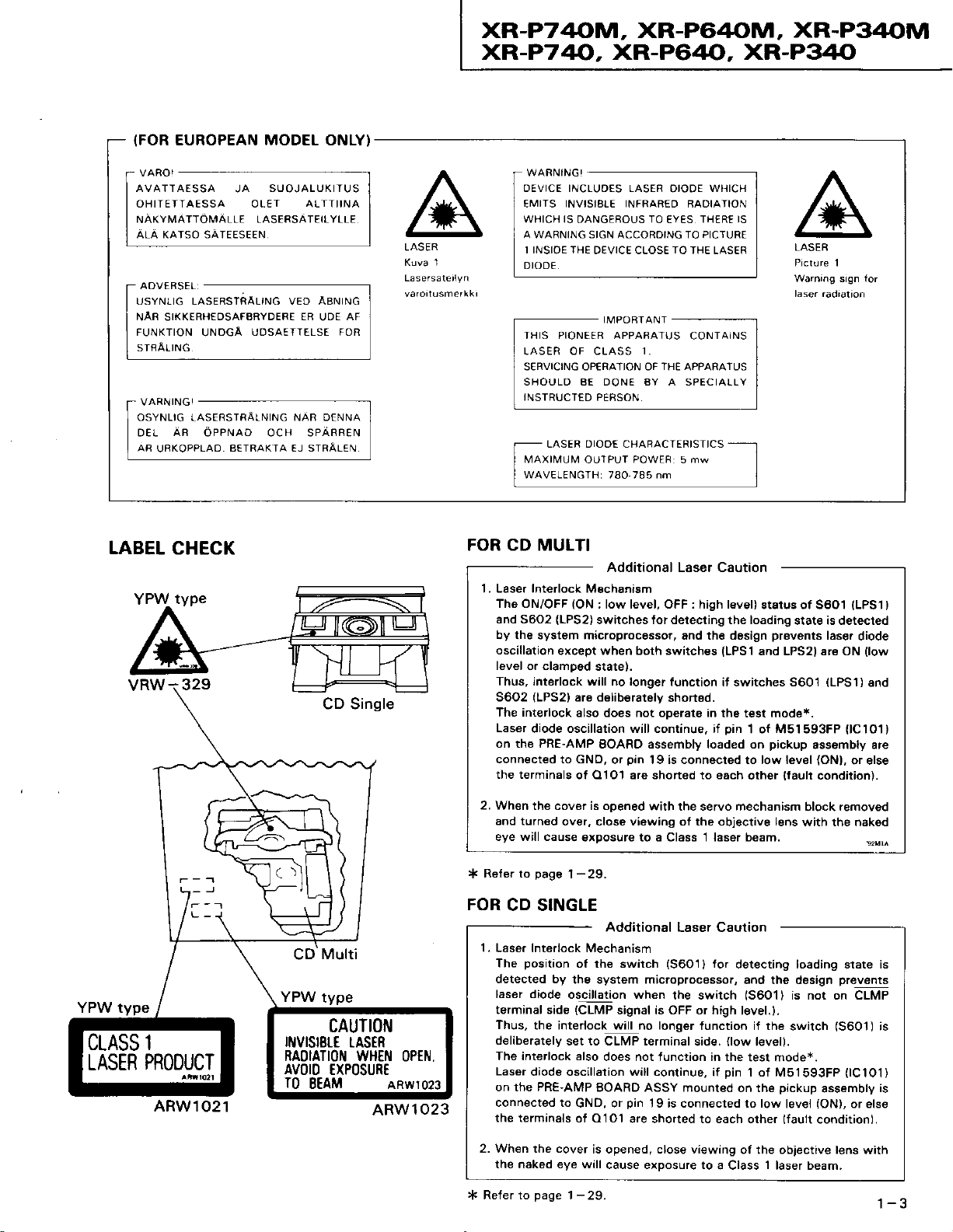
(FOR
EUROPEAN MODEL ONLY}
XR-P74OM, XR-P64OM,
xR-P7
N,
XR-P64(), XR-P34()
XR-P34OM
AVATTAESSA
OHITETTAESSA OL€T ALTTIINA
NAKYMATToMALLE
ALA KATSO SATEESEEN
USYNIIG LASEESTRALING VED ABNING
NAB SIKKERHEDSAFBRYDEFE
FUNKTION
STFALING
OSYNLIG LASEASTRAINING NAB DENNA
D€L
AB
LABET
UNDGA
AB
oPPNAo ocH SPABaEN
URKOPPLAO
CHECK
SUOJALUKITUS
JA
LASERSATEILYLLE
UDSAETTELSE FoR
AETRAKTA EJ STRALEN
ER
UDE
AF
OEVICE INCLUOES LASER
EMITS INVISIBLE INFRABED BADIATION
WI]ICH IS
A WARNING SIGN ACCOROING TO PICTURE
] INSIOE THE
DtooE.
THIS PIONEER APPANATUS
LASER OF CLASS
SERVICING OPERATION OF
SI-IOULD BE DONE BY A SPECIALLY
INSTRUCTED
MAXIMUM
WAVELENGTH: 78O 785 nm
DANGEROUS
DEVICE CLOSE
PERSON
OUTPUT
FOR CD MULTI
1. Laser Interlock Mechanism
Th6 ON/OFF
and S602
by the systern microprocessor,
oscillation
level o. clampgd
Thus, interlock will no longer
(LPS2)
S602
The int€rlock
Laser
diode oscillation will continue. if
on the PRE-AMP
connected to GNO,
the terminal6
: low level, OFF : high lev€l)
{ON
(LPS2)
switches for detecting rhe loading
except when borh switches
state).
are d€liberat€lv
also does not oDerat€ in
EOARD assembly loaded on
or
of O1O1 are shorted to each
WHICH
OIODE
TO
].
POWER: 5 mw
pin
19 is connected to low level
THERE IS
EYES
TO
THE LASER
CONTAINS
THE
APPARATUS
status of 3601
and the design
(LPS1
and LPS2I are ON
lunction it switches 360l
shorted.
the t€st mode*.
pin
1 ot M51593FP
other lfault condition).
stat€ is detected
prevents
pickup
laser
{LPSI)
ass€mbly are
{ON),
(LPS1}
diode
{low
and
{lC101)
or else
CLASS 1
LASER
PRODUCT
ARW1021
CAUTION
[{vrsr8r,E rAsER
RA0tATtot{
AVOIO
T0
EEAM aRw1o23
wHHrl oPtN.
TXPOSUR€
ARW
1 023
2. When
Refer to
tr<
FOR
1.
2. When the cover
Refer to
tr<
the cover is opened
and turn€d
eye will caus€
over, close viewing of the obj€ctive lens
€xposure to a Class 1 laser beam.
-29.
page
1
CD SINGLE
Laser Interlock Mechanism
posilion
The
detecred by
laser diode
terminal side
Thus,
deliberately
The interlock also
Laser
on the PRE-AMP
connected to
the terminals
the naked eve will
of the switch
the system microprocessor,
oscillation when
{CLMP
the interlock will no longer
set to CLMP terminal
diode oscillation will continue,
GND, or
of O1O1
page
1-29.
with the servo mechanism
(5601)for
signal is OFF or high
does not function in the
BOARD ASSY mounted
is opened,
cause exoosure to
the switch
function if rhe
side.
pin
if
pin
19 is connected
are shorted to each other
viewing
close
a Class 1 laser beam.
remov€d
block
with the nakod
detecting loading srare is
and the design
(5601)
is not on CLMP
level,}.
switch
level).
{low
test mode*.
1 of M51593FP
pickup
on the
low
to
level
lfault condition).
of the objective lens
prevents
(5601)is
(lC1O1)
assembty
(ON),
or else
with
is
-J
|
Page 4
XR-P74()M,
xR-P7
Q, XR-P64(),
1.2
SPEC|F|CATIONS
XR-P64()M,
XR-P3@
XR-P340M
STEREO
MULTI-PLAY
n 0 I x3'P,
P3/('M
Ampliftcr
<XR-E
FRON|T
Continuou. Av.ng.
cfiannC, min.,
th.n 1 96..
Continuous
Peak
REAR
Continuous
cf,]{TEn
Continuous Power
<XR-P6,rc/XR-P6,lltM>
FRONT
Continuour
ch.nn.l,
th.n t
Continuous
Peak
REAR
Continuous Power
<XR-P:,IO/XR-P3alll/b
FRONT
Condnuou.
.h.nnal,
th.n I
Continuous Power
Peak Music Power
FM/AM
FM Tunrr
Frgqu€ncy
(9
kHy'l0 kHz
Antenna Input
Alli Tunce
Frequency
Antenna....................
Miscellanaous
Power
Power
Dimensions .....................260
Weight
CD CASSETTE DECK RECEIVER/STEREO
CD CASSETIE DECK
XR-Pr6aO/XR-F6{!M/XR+AO/XR-
&NU
scction
iOlXR-E
lMusic
*.r totll h.rrnonic
Music Power....
.ta.r
a0i/b
Pow.r Oueqt
rt 8 ohm. from
totrl hrrrf|onlc
Power
Outout
Power....
Power
Output
Output
Av.rlgr Powqr
mln., rt 8 ohmr Lom
Power
Output
Output
g.
Avr
min., !t 8
ohm.lrom 50 HarE
tot l hlrrnonic
Output
dirtortion,
{RMS}
(RtvlS).................................
(RMS)......-..........................
Ou$ut i! 70
didortion.
(RMSI
(RMS)
(1
Pow.r Oufprrt
di.tortlon.
(RMS)
50 H.rt with
................ 100
(1
(1
kHz. T.H.D.
(1
kHz, T.H.D.
50 HarE
................
{1
..........................
kHz. T.H.D. 10%.
................._..50
(1
....................................500
tun.r slstion
Soction
Range
step) ..............................7.5
Scc.tlon
Rang€
With 10 kHz
With I kHz
Roquirements
Singapor€
Other mode|
Consumption
(xR-P740lKR-p740M)
(xR-P640r(R-P64oM).
fiR-P3401(R-P340M ) .
(xR-P740t\,1r(R-p640M)
(xn-p740lxn-pan0l
rxR-P34oM)
(xR-p3401........
step .. ........................530
st€p .............................531
model.......................226n'n40
.............. ..1101t2G127l22O/240
.
(XR-P74OAR-P74OMIXR-PAOAR.PAOM}
260
(withour
packagel
..........................................9.5
.
...75
x
371.5
W)
x 310
{W)
. . ....
RECETVER: XR-
i.70 W.ttro
kHz. T.H.D.
W!tt.
with no mor.
kHz. T.H.D. 1oyo.
...............950
i. 33 W.ttr.
with no mora
kHz, T.H.D.
MHz
ohms unbalanced
kHz
kHz
... Loog Antenna
(H)
(H)x
(xR-P340lXR_P340M)
.............. ....
p.r
no mor.
W + 100 W
'10%.
.. ........1050
10%, 16
107o. 16
100 W + 1OO W
to 1,700 kHz
to
.........444lw
.........432
.........276,W
x 295
..........0.2
8 O)
W
1 5 W
O x 2)
1 5 W
O x 2)
pcr
8 O}
W
....15
W
16 O x 2)
p..
W +
W
50
1oYo,
I Ol
w
to 108 MHz
1,602
kHz
V. 50/60 Hz
V.
50/60 Hz
W
mm
{D)
(D)
29S
mm
ko
....e.e ii
..2.a ri
ri
CD Scction
Type................................Compact
Wow and Fluttsr................................
Cassdte deck
Systems
Heads.......................................
Motor .....................................................
Tape
type .............. TYPE |
3.ction
........................
G0.001%
-................
(Normal)
disc digiral audio
Limit ol m66suremont
W.PEAK)
4 track, 2-channel
Record;ng/playbsck
Plavback
Erasing he6d x 1
DC s6rvo motor x 1
tape/TYPE ll
less
or
head x 1
head x 1
(CrO2)
system
(EIAJ)
stereo
tap€
Page 5
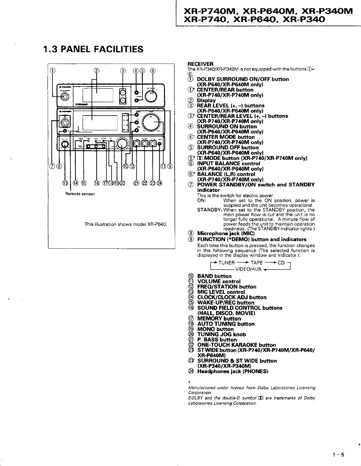
PANEL
1.3
FACILITIES
This rilustratron
shows
model
XR-P640.
XR-P74OM, XR-P64OM,
)(R-P7
Q.
RECEIVER
The XR-P340/XB-P340fi/ is 1ot
a.
DOLBY SURROUND
O)
(XR-P640/XR-P6/OMonly)
^
(1)'
CENTER/REAR button
{XR-P74|!/XR-P740M
_
(?
Display
REAR LEVEL
€)
IXR-P64|!/XR-P640M
^
CENTER/REAR LEVEL
t3'
(XR-P74{I/XR-P740M
^
SURROUND ON button
Qt
(XR-P64O/XR-P6/rcMonly)
^
CENTER
€)'
(XR-P74{,/XR-PT/OMonly}
_
(t
SURBOUND OFF button
IXR-P6/t0/XR-P$oMonly)
^
m MODE bufton
Q)'
INPUT BALANCE control
G)
(XR-P640/XR-P6/0Monly)
^
BALANCE
€)'
(XR-P740/XR-P740M
_
(,
POWER
indicator
rs
This
rhe
ON:
STANDBY: When ser to the STANDBY oosition. the
^
(O
Microphons
(9)
FUNCTION
Each time this button is
in
following
the
displayed
-
I
60
BAND button
ND
VOLUME
02
FREO/STATION button
03
MIG
04)
6b
@
f,
6A
09)
6
al)
6a
LEVEL control
CLOCK/CLOCK ADJ button
WAKE-UP/REC
SOUND FIELD OONTROL buttons
(HALL.
MEMORY
AUTO TUNING
MONO button
TUNING
P. BASS
ONE-TOUCH KARAOKE bufton
STWIDE button
XR-P6/|t!M)
SURROUND & ST WIDE button
@
(xR-P340/XR-P340M)
Hsadphones
@
XR-P6@, XR-P34O
eaurpped
ON/OFF
only}
-)
(+,
buttons
only)
(+,
only}
MODE bufton
(XR-P740/XR-P740M
(L,R)
control
only)
STANDBY/ON
for
switch
When
supplied and the unit becomes operational.
n'arn
longer fully
power
readiness.
in
the display
rUNEB
electfic
set to the ON
power
tlow rs
operational.
feeds
the ,.inrt to
fihe
(MlC)
iack
(TDEMO)
button and
pressed,
sequence
window
-------+
rAPE
vrDEo,/AJX <---------------
control
button
D|SCO. MOVIE)
button
button
JOG knob
button
(XR-P7/O/XR-P74OM/XR-P641)/
(PHONES)
iack
w n the butto4s
button
-l
buttons
swhch and STANDBY
power.
position,
cut and the r,nrt
A minute flow
maintain operation
STANDBY
lThe
indicator lights.)
indicators
the function changes
seiocted
and
-+
tlnction is
indicator.i:
CD
I
XR-P34OM
OF
only)
is
oower
.s
no
of
Manufactured
DOLBY
ta
La bo
under license frcm Dolby Labo?toies Ltcensing
and the double-D symbol @ are trademarks ol
to n e s Li ce n si ng C a rpo ra tton.
Dolby
1-5
Page 6
XR-P74()M,
xR-P7
&,
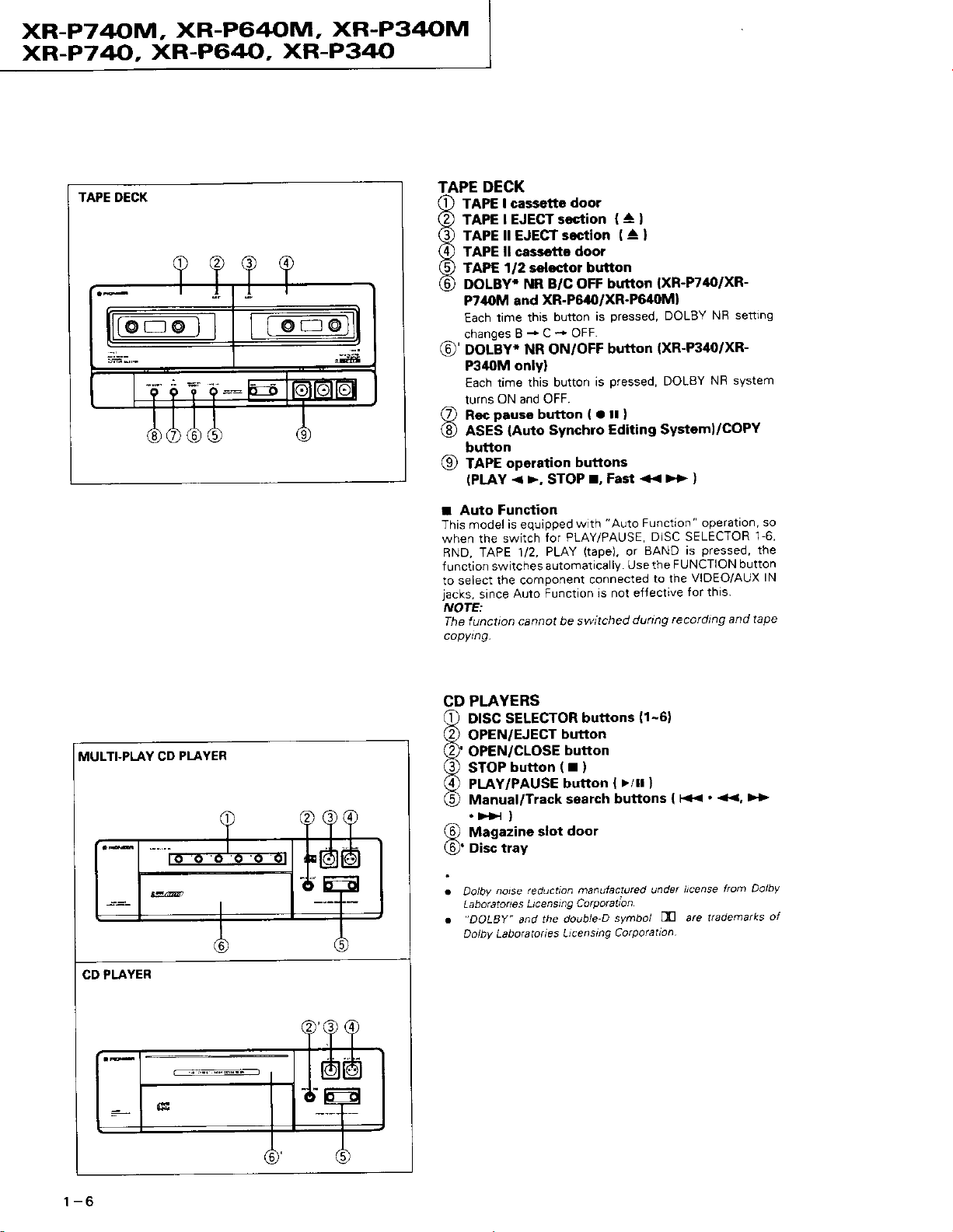
TAPE DECK
XR-P621()M,
XR-P64(),
XR-P34()M
XR-P340
DECK
TAPE
Q
q)
Q)
(4)
6
@
I ca$etto
TAPE
I EJECT soction
TAPE
TAPE ll EJECT
TAPE ll cassctto
fnPt 1/2 soloctor
DOLBY. NR
P?40M and
lime this
Each
chanoesB*C*OFF.
oor--ev.
@'
P3/0M
Each time
turns
CD Rec
aSe-S
tD
button
TAPE
@
(PLAY
NR oN/OFF
only)
this button
ON and OFF.
pause
(nuto
op6ration
>,
<
door
(A)
s.ction
(A
)
door
button
B/C OFF
butron
(XR-P74O/XR-
XR-P6/0/XR-P640M)
button
button
Synchro
STOP
pressed,
is
button
pressed,
is
(
a ll
Editing System)/GOPY
buttons
r, Fast
DOLBY
(XR-P3/o/XR-
DOLEY
)
>>
<<
NB settlng
NR sYstem
)
MULTI-PIAY
PLAYER
CD
Auto Function
I
This model
when the switch
BND. TAPE
function switches automatically.
to select
iacks. since
NOTE:
The
copying.
CD
a
(2)
(3)
(4)
G)
(0.
is
equipped
for PLAY/PAUSE,
PLAY
1/2,
the component
Auto Function
luncton
PLAYERS
DISC
OPEN/EJECT
OPEN/CLOSE
STOPbutton(l)
PLAY/PAUSE
Manual/Track
.
Magazine
Disc tray
Dolby
Laborcton e
-DOLBY"
Dolby Laboratoties
cannot be swlched
SELECTOR
>Dl
)
slot
nolse rcduction
s Lrc e n s
and the
i ng Car
"Auto
wlth
(tape),
or
Use the
connected
ts not eftective
dunng
buttons
button
button
button
search
door
double'D
Ltcensing
>/ll
{
butlons
manufactured under
pot
n.
atto
symbol
Carpatatrcn
Function operatron'
DISC SELECTOR
EAND
to the
(1-6)
}
pressed,
is
FUNCTION
VIDEO/AUX
for this.
recatdng
'
(
K<
hcense
ffi arc trademarks
1-6
the
button
and tape
+<, >>
from Dalbv
so
lN
of
CD PLAYER
-6
I
Page 7
XR-P74()M, XR-P64()M,
xR-P7 N, XR-P640,
XR-P34()
XR-P340M
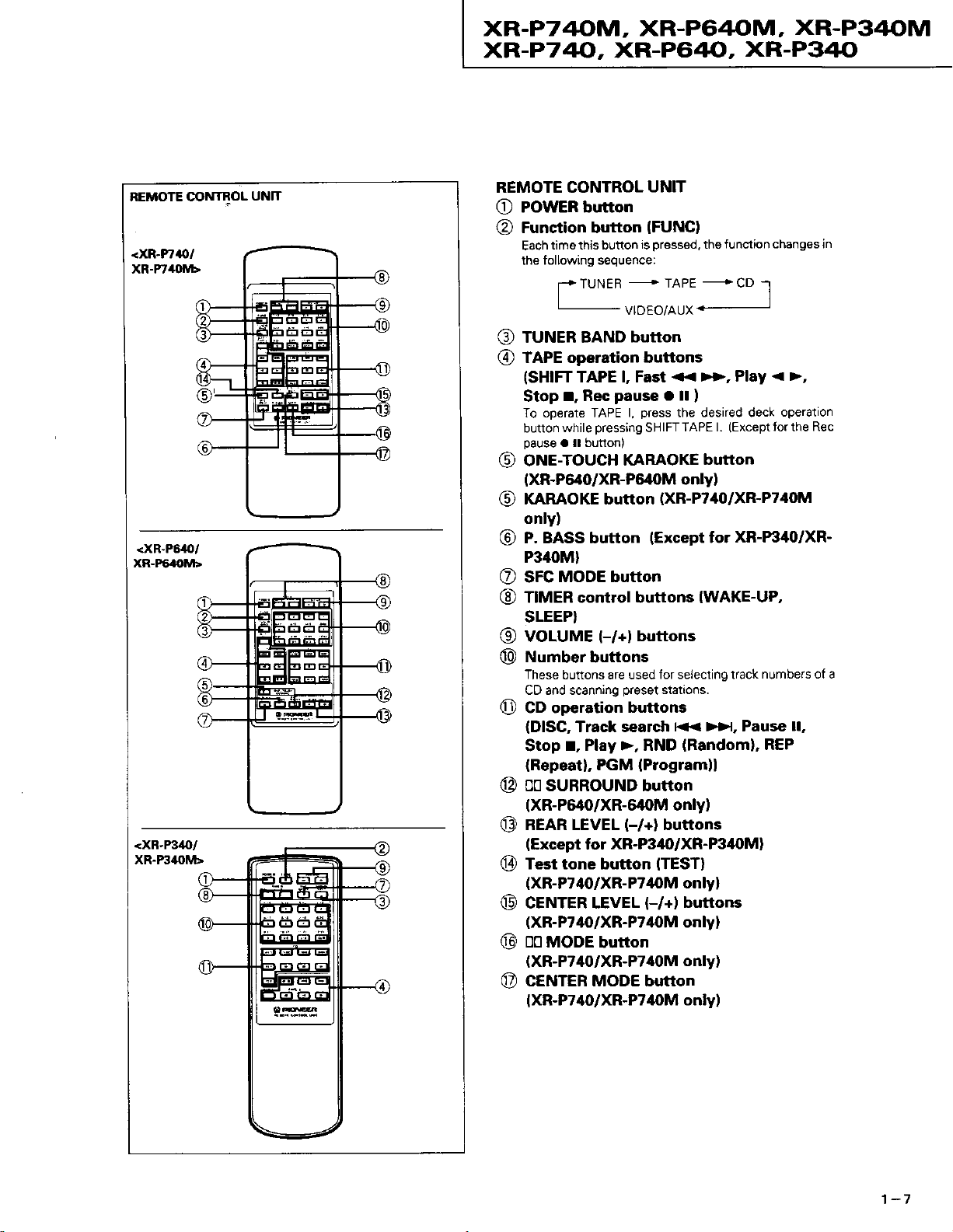
REMOTE CONTROL
UN]T
REMOTE CONTROL
PowER butron
O
Function button
@
timethis button
Each
following sequence:
the
TUNER BAND
TAPE op€ration buttons
@
{SHIFT
Stop
To operate TAPE
buttonwhile
pause
TAPE 1, 56s1
r, Rec
a ll button)
is
+
VIDEO/AUX
bufton
pause
press
l.
pressing
SHIFTTAPE
ONE-TOUCH KABAOKE
(XR-P640/xR-P640M
,G)
KARAOKE button
onlyl
P. BASS button
@
P340Ml
MODE button
SFC
@
TIMER control buttons
@
SLEEP}
6l
VOLUME
Number buttons
@
These
CD and scanning
CD operation
o
{DISC,
Stop
(Repeatl,
D0 SURROUND button
@
(-/+l
buttons
buttons are used
preset
buttons
Track search
r, Play >, RND
(Programll
PGM
{XR-P640/XR-6/I0M
REAR LEVEL
@
(Except
Test tone button
@
(-/+)
for XR-P34O/XR-P34{!M}
(XR-P740/XR-P7'OM
CENTER LEVEL
@
(-/+l
(XR-P740/XR-P7'OM
DC MODE
@
button
(XR-P740/XR-P7t[0M
CEIITER MODE button
@
{XR-P740/XR-P7'l{)M
UNIT
(FUNCI
pressed,
TAPE
11 >>, Play
a ll
the desired deck
function changes in
the
l
(Excepttorthe
l.
< >,
operation
button
only)
(XR-P7II0/XR-P740M
(Except
XR-PI|40/XR-
fot
(WAKE-UP,
for selecting track
stations.
K< >>, Pause
(Randoml,
numbers ol a
ll,
REP
only}
buttons
{TESTI
onlyl
buttons
only)
only]
onlyl
Rec
Page 8
XR-P74()M,
xF|-P7 40, XR-P640,
XR-P640M, XR-P34()M
XR-P34()
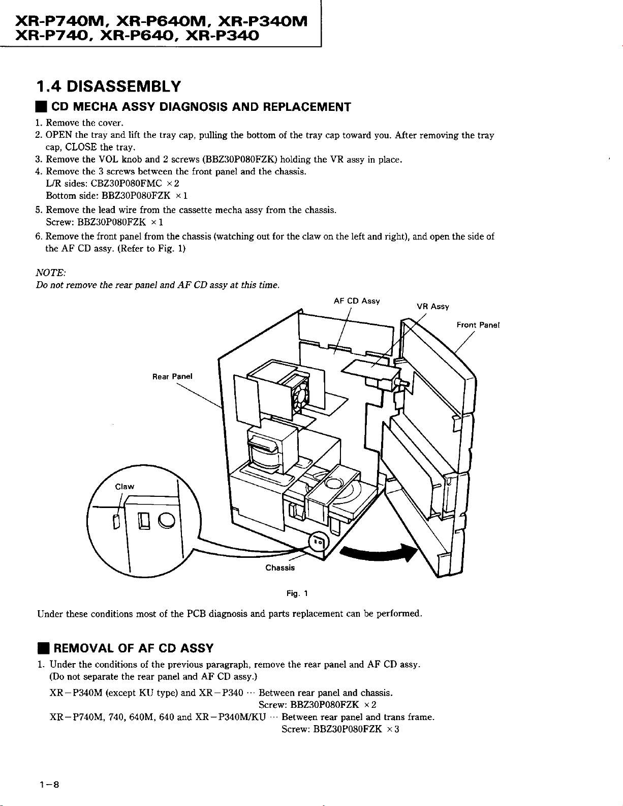
1.4 DISASSEMBLY
CD MECHA ASSY DIAGNOSIS AND REPLACEMENT
T
1. Remove the cover.
2. OPEN the tray and lift
cap,
CLOSE the tray.
3. Remove the VOL knob and 2 screws
4. Remove the 3 screws between the front
L/R sides: CBZ30P080FMC
Bottom side: BBZ30P080FZK x 1
5. Remove the lead wire from the cassette mecha assv from the chassis.
Screw: BBZ30P080FZK x I
assy.
panel
(Refer
6. Remove the front
the AF
NOTE:
Do not remove the rear
CD
tray
the
x2
from the chassis
Fig. 1)
to
panel
and AF CD assy at this time.
pulling
cap,
(BBZ30P080FZK)
Danel and
(watching
the bottom of the tray cap toward
holding the VR
the chassis.
out for the claw on the left
assy in
and right), and open the side of
AF CD Assy
you.
After removing the
place.
tray
these conditions most of the PCB diagnosis
Under
REMOVAL OF AF CD ASSY
I
1. Under the conditions of the
(Do
not separate the rear
XR-P340M
XR-P740M,
1-8
(except
740, 640M, 640 and
previous paragraph,
panel
and
KU type) and XR P340
and
remove the
AF
CD assy.)
. .
XR-P340IWKU
Fig. I
parts
replacement can be
panel
rear
Between rear
Screw: BBZ30P080FZK
. .
Between rear
Screw:
panel
BBZ30P080FZK
and A-F CD assy.
and chassis.
panel
performed.
x2
trans frame.
and
x3
Page 9
XR-P740M,
xR-P740,
XR-P640M,
XR-P64{J--,
XR-P340M
XR-P34.o
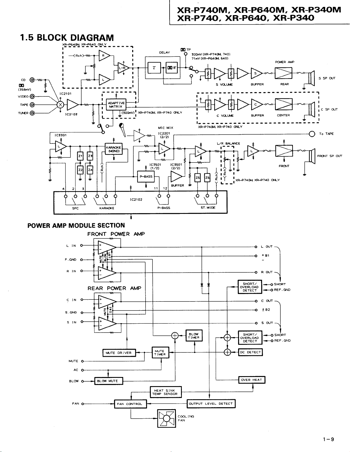
1.5 BLOCK
DIAGRAM
XR--P64O\I, XR-P640 ONLY
-<
!
I
I
I
I
I
I
lc21 03
tc3301
""n
I
I
I
I
)cup740M xR-P74o o.LY
l:oorntl!
I
MIC MIX
tc2201
(2/21
rcr501 1c3501
(/21
Q/2)
(XFI-P7401,(
30omv
(XR-P54O'{
71nV
S VO-Lri€
rt
I
c
t-
- -
-
XR-P740M XR-P740
L,/R
I
I
$
7a0)
E40)
I
vo|-t.tiC
otl-Y
BAI-A€E
tfll
rl
lr
t
l'i
'5'
t
r&
;-Y_ _i**74o*
B\TFFER
BIJFFER
x*74o o^{-Y
POAER
REAR
CENTER
AI'IP
S SP OUT
't
I
I
I
o{JT
c sP
I
I
I
ro TAPE
FRONT SP OUT
POWER AMP MODULE
FRONIT PO\A'ER
REAR
MUTE
AC
BLc)\IV
SECTION
PCTA/ER AT4P
AN,IP
L OVT
l
:"'
-.1
R O(,'T
I
l<,
::r:,."
C O'JT
l
!82
S OTJT
-l
l--.o
:::::'."
l+-o
I
I
I
I
I
I
I
OUTPUT LEVEL
r.rc
cooL I
FAN
DETECT
1-9
Page 10
XR-P740M,
XR-P64()M,
XR-P340M
xR-P7 44, XR-P640, XR-P34()
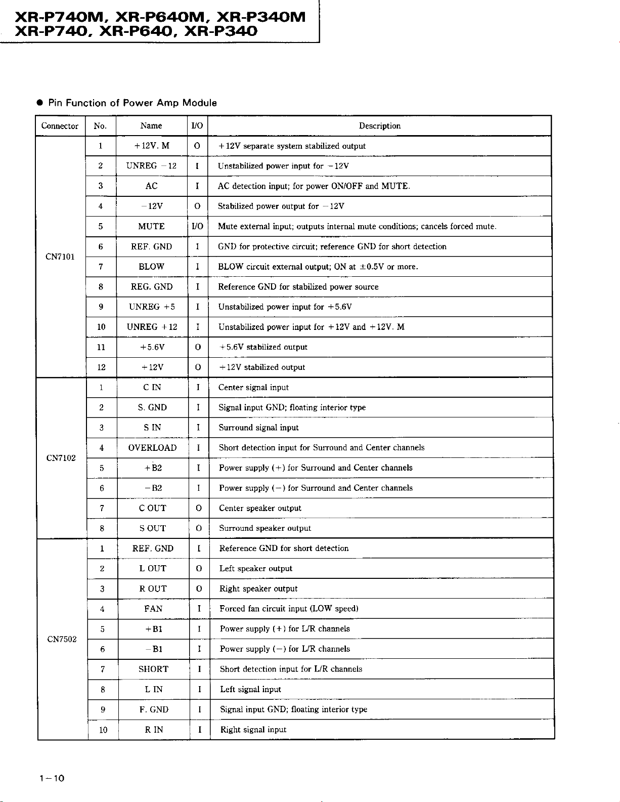
a
Pin
Function
Power Amo
of
Module
Connector
cN7l01
No.
2 UNREG
3
4
5 MUTE
6 REF, GND I GND
7 BLOW I BLOW circuit extemal output; ON at
8 REG. GND I Reference GND for stabilized
9 UNREG
10 UNREG + 12 I Unstabilized
11
T2
1 CIN I Center signal input
Name UO
+ 12V.
M o
12 Unstabilized
+
12V separate system stabilized output
power
AC I AC detecrion input: for
tzv o Stabilized
power
vo Mute external input; outputs intemal mut€ conditions; cancels forced mute.
protective
Ior
power
power
stabilized output
+5.6V
+t2v
+5
I Unstabilized
+5.6V stabilized output
o
+
o
12V
input for
output for - 12V
circuit;
input for
input for
-
12V
power
ON/OFF and MUTE.
reference GND for
power
+5.6V
+12V
2 S. GND I Signal input GND; floating interior type
Description
:t0.5V
source
+12V.
and
short detection
or mo!e.
M
cN7l02
cN7502
3 srN
4 OVERLOAD I Short
5
6
+82
82 I Power supply
7 C OUT
8 S OUT o
I REF. GND I Reference
I Surround signal input
detection input for Surround and Center channels
I Power supply
o Center speaker output
Surround speaker output
GND lor short detection
2 L OUT o Left speaker
3
4 FAN I
5
6 B1
7
R
OUT o
+81
SHORT Short detection
8 LIN
9 F. GND
Right speaker output
Forced fan circuit input
Power supply
I
Power supply
Left signal input
Signal input GND; floating interior type
(+)
for Surround and Center channels
(-)
for Surrcund and Center channels
output
(LOW
speed)
(*)
for L/R channels
(
for L/R channels
)
input for I-./R channels
10
RIN Right signal
input
Page 11
IC INFORMATION
1.6
XR-P740M, XR-P640M,
xR-P7
40,
XR-P64trJ_,
XR-P340
XR-P34()M
c
The information
may not correspond exactly
and
shown in the
schematic diagrams.
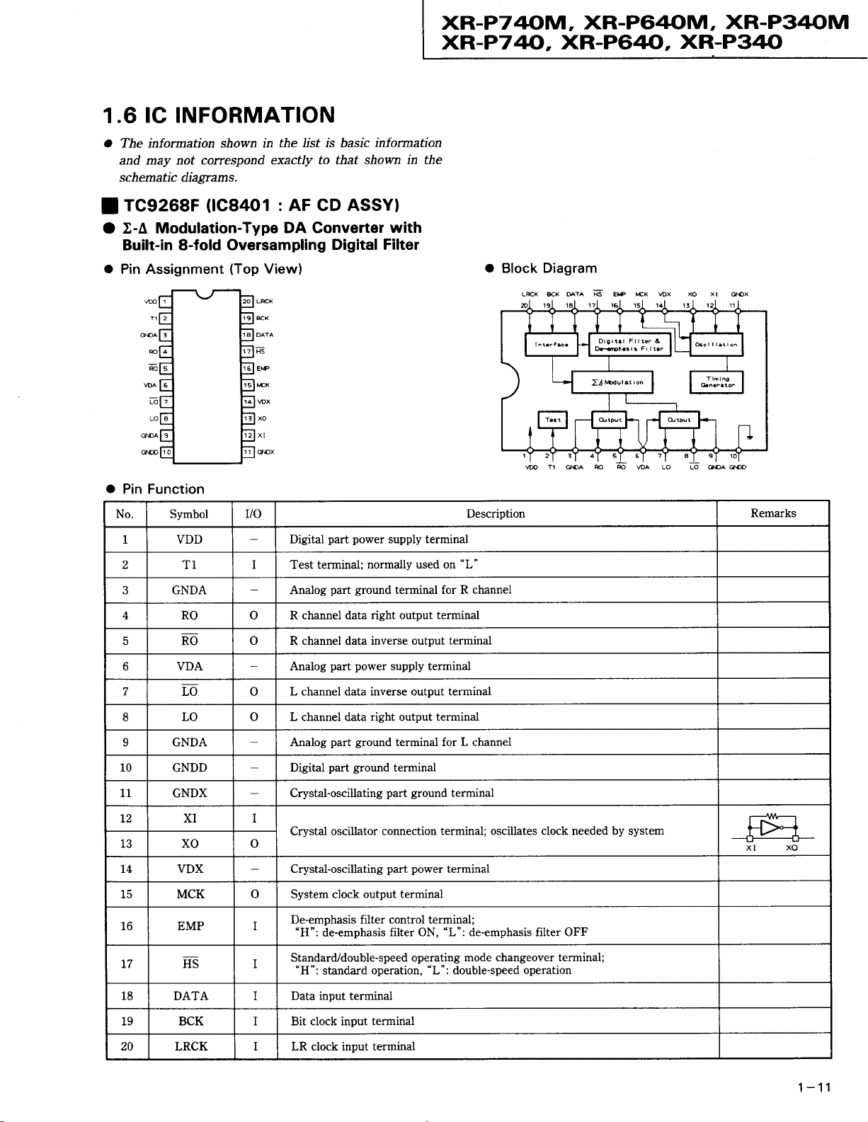
rc9268F
I
O X-A
ilc84o1
Modulation-Type
: AF cD AssY)
DA Converter
Built-in 8-fold Oversampling
o
Pin Assignment
WA
-
o
Pin Function
No. Symbol
I VDD Digital
2
T1
(Top
LrcX
rcK
EF
WX
xo
XI
NX
VO
I
View)
list is basic information
to that shown
with
Digital Filter
part power
Test terminal; normally
supply terminal
in
the
used on
o
Block Diagram
Description
"L"
LrcK MX MTA K EF rcK WX
Remarks
GNDA Analog
4 RO o R channel data right output
RO
6
VDA Analog
o R channel data inverse output
7 LO o
8 LO o L channel data right output
9 GNDA
10
ll
GNDD
GNDX
part ground
part power
L channel data inverse output terminal
part ground
Analog
part
Digital
Crystal-oscillating
terminal for R channel
supply
terminal for L channel
ground
terminal
part ground
L2 XI I
IJ XO o
t4
vDx
15 MCK o System clock
16 EMP I
L7 HS I
18
DATA
I Data input terminal
r
Crystal-oscillating
De-emphasis filter control terminal;
"H":
de-emphasis
Standard/double-speed operating
"H":
standard
part power
output terminal
filter ON,
operation,
terminal
terminal
terminal
terminal
terminal
terminal
"L":
de-emphasis filter OFF
mode changeover terminal;
"L":
double-speed operation
19 BCK I Bit clock input
20
LRCK
LR clock input terminal
terminal
1-11
Page 12
XR-P740M,
xR-P7
40,
XR-P640M,
XR-P6
Q, XR-P340
XR-P340M
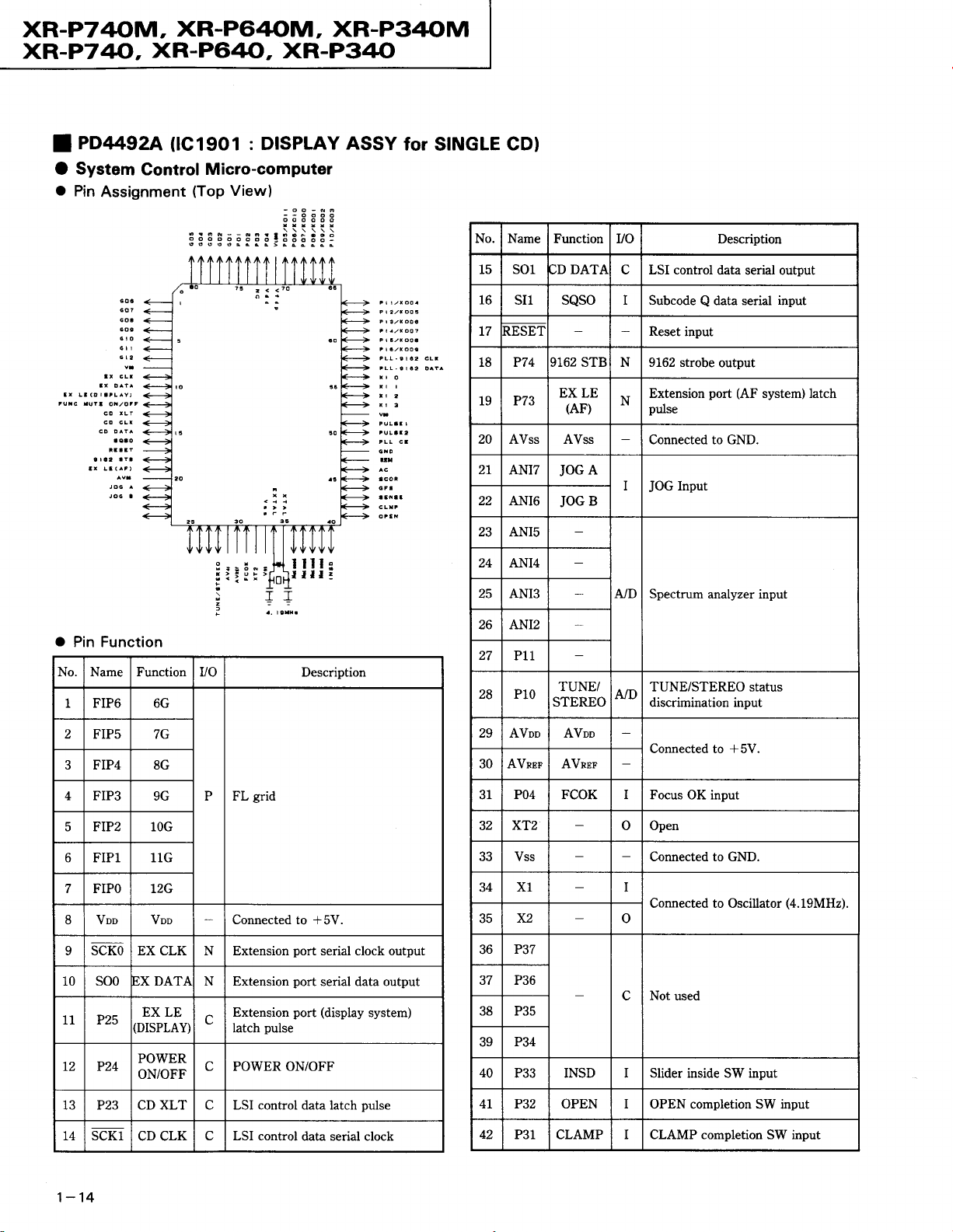
PD4493A
I
System
O
o
Pin
Assignment
Et LE(DISPL^Y)
:
{tC19O1
DtSpLAy
Control Micro-computer
(Top
View)
GO.
?
60
60a
609
cro
-T'
T
V',
tt
ASSY
for
MULTT
CDI
No.
Name Function
15
so1 ]D
16
SIl SQSO
L7
IESEl
l8 P74
19
P73
20
AVss AVss
2l
ANIT
22 ANI6
23
ANIs
24 ANI4
25 ANI3
vo
DAT/
}162 STB N
EX LE
(AF)
A
JOG
B
JOG
A/D
c LSI control
I
Subcode Q data
Reset
input
9162 strobe
Extension
N
pulse
Connected to
Input
JOG
Spectrum analyzer
Description
data
serial outout
serial
output
(AF
port
GND.
input
system)
input
latch
O
Pin
Function
No.
Name Function
I FIP6
2 FIPs
3 FIP4
4
FIP3 9G
5
FIP2 10G
t)
FIPl
FIPO rzc
8 Voo Vop
9
SCKO EX
10
so0 'X DATI
11 P25
T2 P24
,DISPLAY'c
POWER
ON/OFF
VO
6G
7G
8G
P FL
11G
Connected to *5V.
CLK N Extension
N Extension
EX LE
Extension
latch
C POWER
grid
oulse
Description
port
serial clock
port
serial data
(display
port
ON/OFF
output
output
system)
26 ANI2
27
Pl1
28
P10
29 AVoo
30 AVnrr
31
P04 FCOK
32 xT2
33 Vss
TUNE/
STEREO
AVoo
AVnrr
TUNE/STEREO
A/D
discrimination input
Connected to +5V.
I Focus OK input
o Open
Connected to GND.
34 X1
x2
35
36
P37 DCNT I Disc count
37 P36
P35
38
39 P34
40
DCHM I Disc selector home
MZSZ
MZSl
P33 INSD I Slider inside SW input
o
I
pulse
status
input
SW
IJ
P23
L4 SCKl
1-12
CD XLT
CD CLK t-
L
LSI control data latch
LSI control
oulse
data serial clock
4l P32 LP52
I
42 P31 IPSl
Page 13
XR-P74()M,
xR-P7 &,
XR-P640M,
XR-P640,
XR-P34()M
XR-P34()
1 reel
Description
pulse
pulse
pulse
+5V.
No. Name Function uo
LSI operating status multi-mode
P30 SENS
44 P03 GFS I
45 INTP2 SCOR I Subcode synch SO
46 INTPl
47 INTPO REM I Remote control
48 tc Connected to GND.
49 P72 PLL CE PLL latch
50 P71 PULSE2
51 P70 PULSEl I Tape
52
PI27
PT26
55 P125
56 P124
57 P123
AC I AC input
PLL 9162
DATA/
KO11
I
iDput
Frame/syncMock input
I Tape 2 reel
Connected to
I Key scan i[put
P PLL and 9162 serial data
+ SI input
sigrral input
input
input
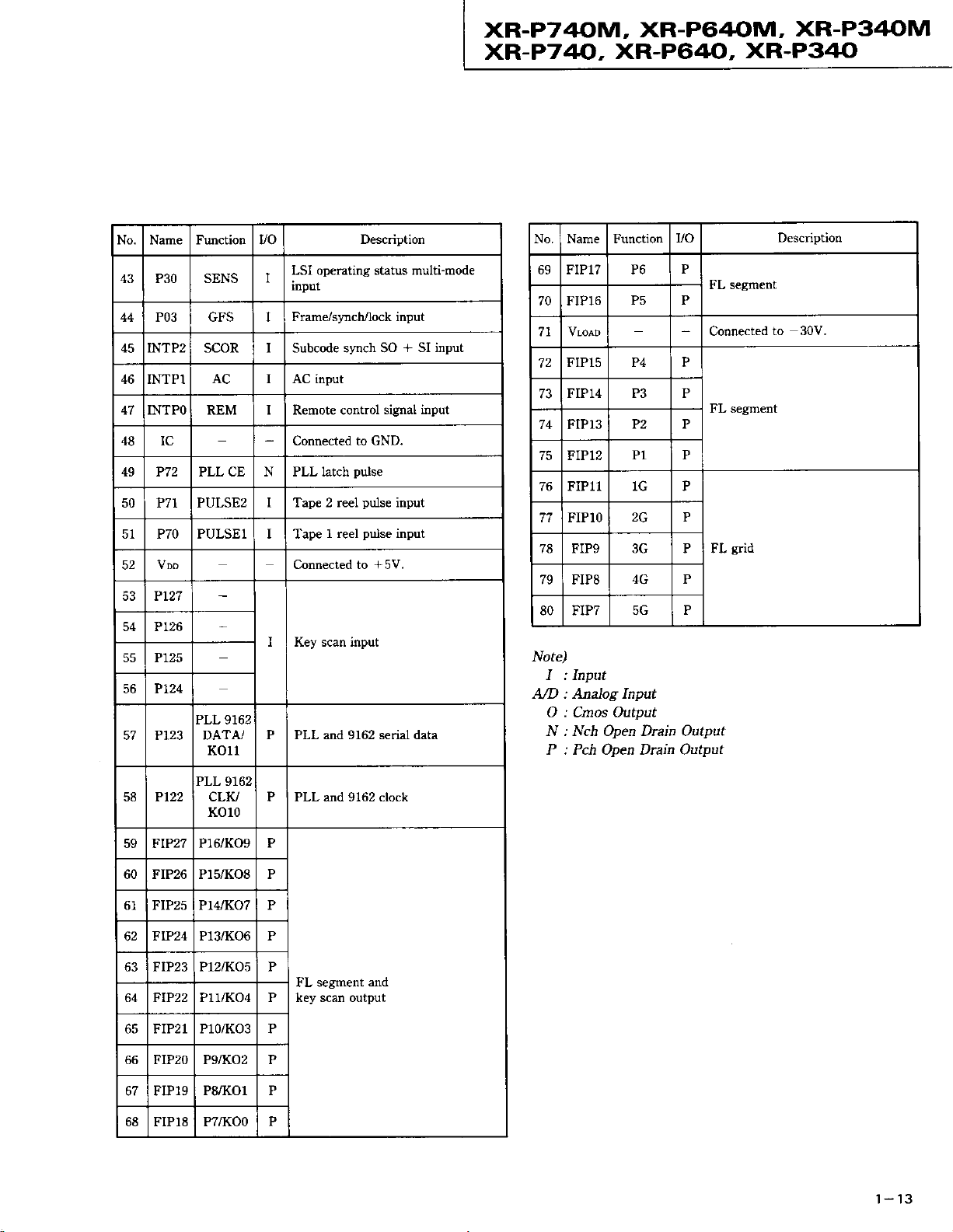
No. Name Function
69 FIP17 P6
70 FIP16
71
FIP15 P4 P
72
FIP].4 P3 P
73
74 FIP13
75 FIP12
76 FIP11 P
77 FIPlO
78 FIPg 3G P
79 FIP8
80 F1P7 5G
vo
P
P5 P
P2 P
P1 P
2G P
4G P
P
Note)
I : Input
A/D : Analog Input
O :
Cmos
Artput
N : Nch Open Drain Output
P : Pch Open Drain Output
FL segment
Connected
FL segment
grid
FL
Description
to 30V.
PLL 9762
P122
59 FIP27
60 FIP26 P15/KO8 P
FIP25 Pr4tKOT P
FIP24 P13/KO6 P
62
FIP23 P12lKO5 P
63
64 FIP22 P11/KO4 P
FIP21 P1o/KO3 P
66 FIPzO P9tKO2 P
FIP19
68 FIP18 P7lKO0
cLw
KO10
P16/KO9 P
P8/KO1 P
P PLL and 9162 clock
FL segment
key scan output
P
and
Page 14
XR-P7@M,
xR-P7
&,
XR-P640M,
XR-P64{J_,
XR-P340M
XR-P340
PD4492A
I
System
O
o
Pin
Assignment
lr cLr
ar o^i^
ar Ll(oratLAY)
Control
GO6
co?
coa
coa
6ro
Gr r
6ta
{lC19O1
: DISPLAY
Micro-computel
(Top
View)
_0i!,))))))
oooo:
oooooo
ASSY
ltr
for
SINGLE
CDI
No. Name
15 so1
16
L7 Reset
RESEl
18 P74 )162 STB N 9162 strobe
19 P73
20 AVss AVss
2l
22 ANI6
23 ANI5
24 ANI4
25 ANI3
Function uo
]D DATA c LSI control
SI1 SQSO Subcode
ANIT
EX LE
(AF)
JOG
JOG
A
B
Extension
N
pulse
Connected to GND.
Input
JOG
A/D Spectrum
input
Description
data serial outout
data serial
Q
output
(AF
port
analyzer input
system) latch
input
o
Pin Function
No. Name Function
I
FIP6 6G
VO Description
2 FIP5 7G
J
FIP4 8G
4 FIP3
9G
P FL
grid
5 FIP2 10G
o
FIPl 1lG
FIPO L2G
Vno Voo Connected to +5V.
8
9 SCKO EX CLK N Extension
10 so0 ]X DATT N Extension
11 P25
12 P24
EX LE
DISPLAY)
POWER
ON/OFF
Extension
c
latch
pulse
c POWER ON/OFF
port
serial clock output
port
serial data output
(display
port
system)
26 AN12
27
P11
28 P10
TUNE/
STEREO
TUNE/STEREO status
A/D
discrimination input
29 AVoo AVoo
30 AVnBr AVnBn
Connected to
31 P04 FCOK I
xT2
32
JJ
Vss Connected to GND.
Focus OK input
o Open
34 x1 I
x2
35
36
JI
P37
P36
o
c Not used
38 P35
P34
39
40
P33 INSD I Slider inside SW input
+5V.
P23 CD XLT c LSI control data latch
l4 SCKl
CD CLK
c LSI control
1- 14
pulse
data serial clock
47 P32 OPEN I
42
P31 CLAMP I CLAMP completion SW input
OPEN completion SW input
Page 15
XR-P74OM,
XR-P64OM.
xR-P7 &, XR-P64(),
XR-P34OM
XR-P34()
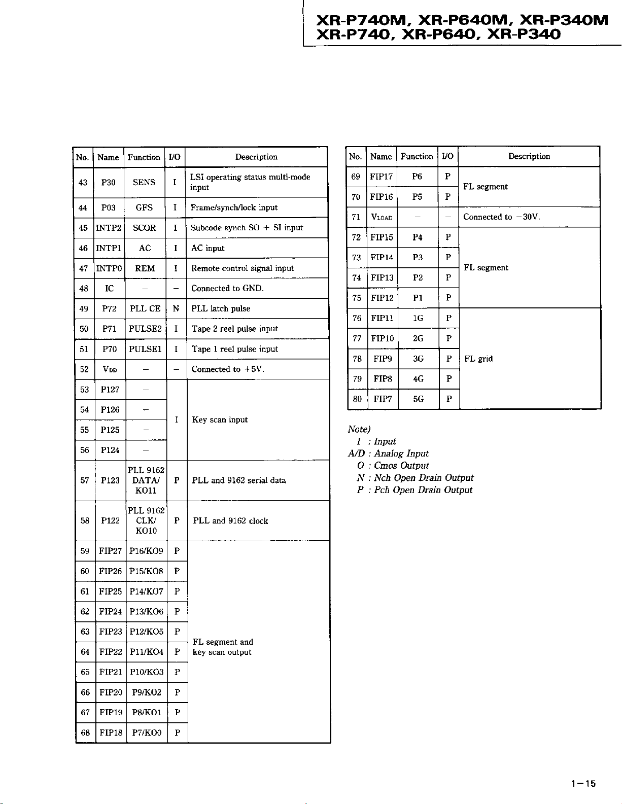
No. Name Function
43 P30 SENS
44 P03 GFS I
45 INTP2 SCOR I Subcode synch
46
INTPl AC I
INTPO REM I Remote
4a IC Comected
49 P72 PLL CE N PLL latch
50
52 Conoected to
53 Pt27
54 PL26
55 Pl25
PULSE2 I Tape 2 reel
P70 PULSEl I Tape
Pt24
PLL 9162
Pt23
DATA.i
KO11
uo Description
LSI operating status
I
input
Frame/syncMock input
AC input
control signal input
to GND.
pulse
I reel
Key scan
PLL and 9162 serial data
input
SO + SI input
pulse
input
pulse
input
+5V.
multi-mode
No. Name Furction
69 FIP17
FIP16 P5 P
70
7L
FIP15 P4 P
FIPl4 P3 P
73
FIP13 P2
74
FIP12 P1
76 FIP1l P
77 FIPlO
78 FIP9 3G P
FIP8 4G P
79
80 FIPT 5G
Note)
I : Input
A/D : Analog Input
O : Cmos Output
N : Nch Open Ihain Output
P : Pch Open Drain Output
UO Description
P6 P
2G P
FL segment
Connected to
FL segment
P
FL
P
-30V.
Srid
5at
Pt22
CLIv
KO10
PLL 9162
59 FIP27 P16/KO9 P
60
FIP26 P1s/KO8
FIP25 P14|KOT P
62 FIP24 P13/KO6 P
63 FIP23 P12lKO5 P
u F]P22 P11/KO4
65 FIP2l P10/KO3
66 FIP2O P9tKO2 P
FIP19 P8/KO1 P
68 FIP18
P7lKO0 P
P PLL and 9162
P
FL segmelt and
V
key scan output
P
clock
t-t5
Page 16
XR-P740M,
xR-P7
Q, XR-P64(),
XR-P640M,
XR-P340
XR-P34()M
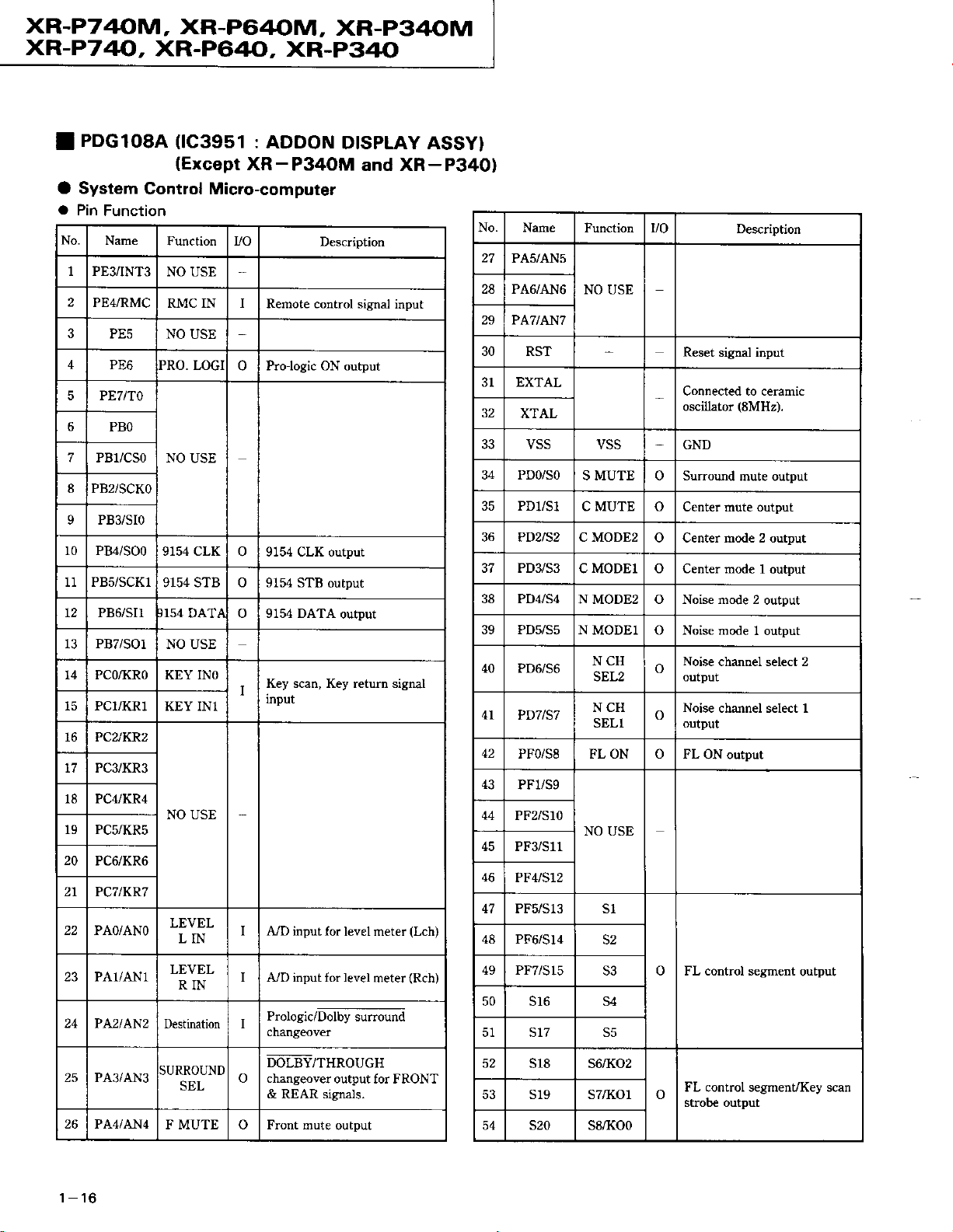
pDGtoSA
I
flc3951
(Except
O System
a
Pin
No.
1 PE3/INT3
2
PE4/RMC
3
4 PE6
5 PE7ITO
6
7 PBl/CSO
8 PB2|SCKO
10 P84/SOO
11 PB5/SCKl
t2 PB6/511 )154
13 PB7/SOi
14 PCO/KRO KEY INO
PCi/KR1
PC2IKR2
17 PC3/KR3
18 PC4/KR4
19 PC5/KR5
20
PC6/KR6
2l PCTIKRT
22 PAO/ANO
Control Micro-computer
Function
Name
PE5 NO
PBO
PB3/SIO
Function to
NO USE
RMC IN I
USE
PRO. LOGI
NO
USE
9154 CLK
9154 STB o 9154 STB
DATA o 9154 DATA
NO USE
KEY IN1
NO USE
LEVEL
LIN
:
ADDoN
XR-P34OM
Remote control signal
DtspLAy Assy)
and XR-P34Ol
Description
o Prologic ON output
o 9154 CLK output
output
output
Key scan, Key retum signal
I
rnput
I A/D input for
level meter
i[put
(Lch)
No. Name
27
PAs/AN5
28 PA6/AN6
29 PA7/AN7
30 RST
EXTAL
32
XTAL
33 VSS
34 PDO/SO
PD1/S1
36 PD2t32 C MODE2
PD3/S3
38 PD4/S4
39 PDs/S5
40 PD6/S6
4l
PD7lS7
42
PF0/S8 FL ON o FL
43
PF1/S9
44
PF2/S10
45
PF3/S11
46
PF4/S12
47 PFs/Sr.3
48 PF6/S14
Function vo
NO USE
VSS GND
S MUTE o Surround
C MUTE o
C MODE1 o Center mode 1
N MODE2 o Noise mode 2
N MODE1 o Noise mode
NCH
SEL2
NCH
SELl
NO USE
S2
Descliption
Reset
signal input
Connected to ceramic
oscillator
Center mute output
(8MHz).
mute output
o Center mode 2 output
output
output
I output
Noise
o
o
channel select 2
output
Noise
channel select I
output
ON output
23 PA1/AN1
24 PA2iAN2
25 PA3/AN3
26 PA4/AN4
| - to
LEVEL
RIN
Destination I
SURROUND
SEL
F MUTE o Front mute
I A/D input for level
Prologic/Dolby
changeover
DOLBY/THROUGH
o
changeove!
& REAR signals.
(Rch)
meter
surround
output for FRONT
output
49 PF7/S15
50 S4
S3
s17
52
s18 s6/KO2
s19 s7/KO1
54 s20
s8/KO0
o FL control segment
FL control segment/Key scan
o
stlok output
output
Page 17
XR-P7@M,
XR-P64OM,
XR-P34OM
xR-P7 40, XR-P64(), XR-P3ZU)
No. Name Function UO Description
T15/S21 S9
'ft4ls22
57 Tr3/S23
'tt2ts24
58
59 Tli/525
60 Tr0/s26 s14
T9tS27
62 T8/528 st6
63 T7
64 T6
65 T5
s10
sl1
s12
NO
sl3
USE
FL control segment
o
output
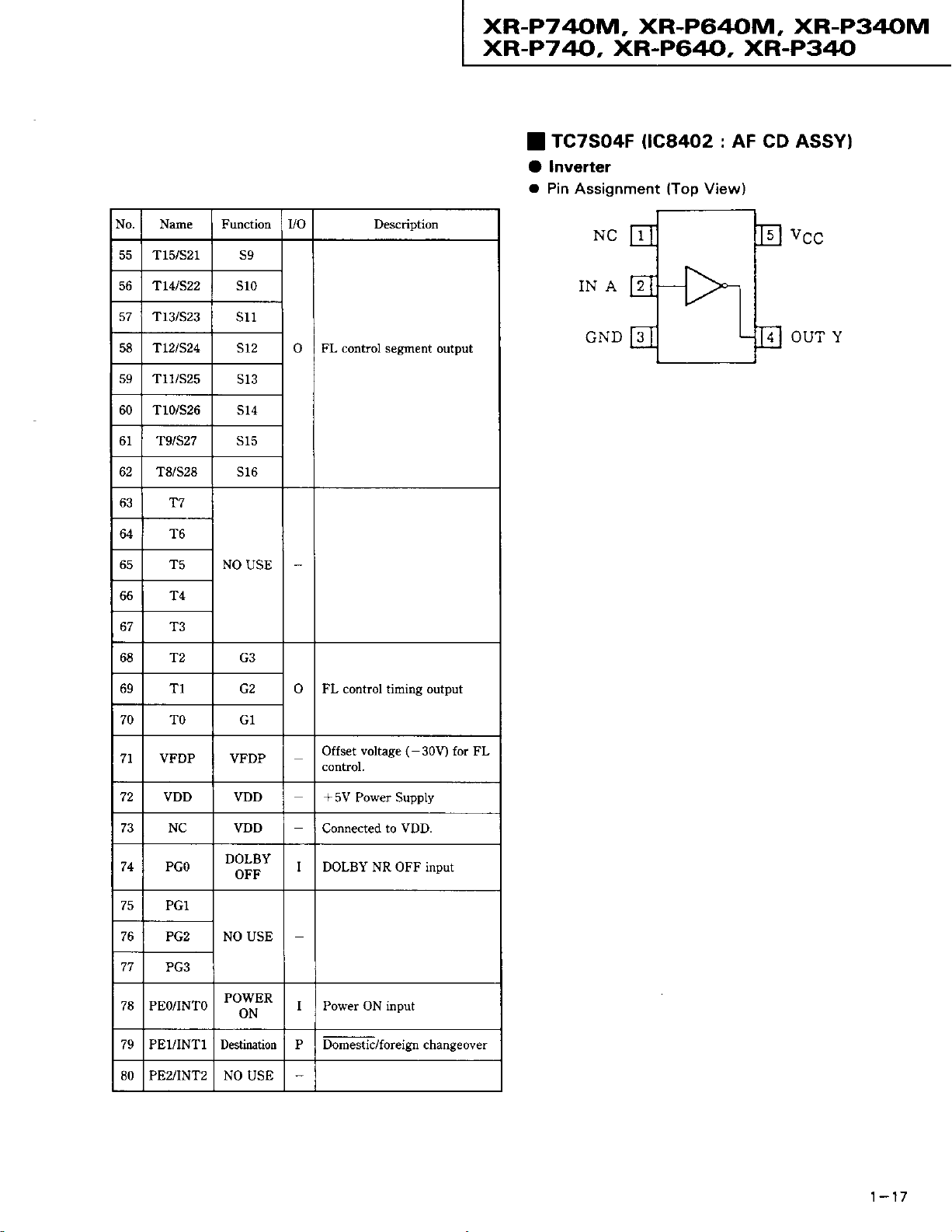
TcTso4F
I
lnverter
O
a
Pin
Assignment
INA
GND
0c8402
View)
{Top
: AF
GD
OUT Y
ASSYI
66 T4
T3
68 T2
69
70 TO G1
71 VFDP VFDP
72 VDD VDD +5V Power
75 PG1
77
78 PEO/INTO
79 PE1/INT1 Destination P Domestic/foreiSn changeover
TI G2
NC VDD
PGO
PG3
DOLBY
OFF
NO USEPG2
POWER
ON
o FL control timing output
(-30V)
voltage
Offset
control,
Supply
Connected to
I DOLBY NR OFF input
I Power ON input
VDD.
for FL
80 PE2NNT2 NO
USE
Page 18
)(R.P7
4OM.
xR-P74(),
XR-P64OM,
XR-P34OM
XR-P64{), XR-P340
AAVTOO2
I
FL Tube
O
o
Grid
Assignment
rCI0
o
Assignment
Pin
(Vl7O1
: DISPLAY
t]S n nill fltNfi frl\V'll
uvvIYJ4 $'uvue v!llj,
UN
ASSY)
B8E
ot--
ooL-
tFrll
nnno
IA\UIEU DO BO REPEAT
5
RNCI
Rll lBltD
MEC
PGM
n3mnS>
uffi"
@TIMER
WAKEUP
tn
m"nmnh"mcfu
a?||1{l tYl
O
Pin Connection
Sl
6
4i
8l
7
\ 2 3
s n0 nn n2i
------\sr -
Oqr
83f=
Bzc=
8rf=
=18r6
-lo1tr
-Jorq
-
-)otz
=1811
=1810
=f
(12G-9G)
h\:- A
/ i nhn,
|1\\n // n6
| \1nt/ 1l
v9 v h v
O-
,,tfl
0
"//////\\
lltl lJo \\ l,
v ull
llu
z-,V
d
(
7G-3G )
88t-:
ot|€
ooL€
oql...._
83t-:
82r:
89 Brt-:
kn
/ /
x" fl
/i"
(BG)
-.-
an
o
Anode Connection
t2G
P]
P2 82 B2
P3 83 B3
QA
P5
P6
P7
P8 BB BB
P3 8S
Pta 8r8
Pr1 Brl Bll
rtz
a|2
Pl3
813
al A
P14
Pl5
Pl6
P17
r00
llG
8l
QA AA
B1
B5 B5
B6 B6
87 B7
83 B9
8ra 810
ai2
Br3
814
815 815
Br6
Br6
til
6),
toG 9G BG
B1
B2
B3
B4
85
86
B7 B7
BB
Bll
812 812
813 813
814
815 Br5
816 Br6
IK t.3K
B]
B2
B3
a/ QA
85 B5
B6
BB
B9
B1A
811
<ralr>
ff
[(Drsco)J.J
l.L(MOvlE)JJ
TUNEO
4
81
STEffiO
!0(
B1
B2
B3
B6
B?
BB
)
mm
CIOPV
ASES
ss
l)
NOTE
2)
3) DL
4)
7G
AM
Fil
6G 5G
co12
n n n n
e e
I s s
b
k k k k
)
d d d
p p
r
c
m m
I I
n h h n
o
b
) )
c
m m
I
co0l
Fl,F2
------
NP
______
1G-12G
4G 3G
kffir
e
s
b
d
c
o
k
J
d
r
t
r
c
m
{
h
ffift
---
Fi0ament
No
Pin
Datum
---
Grid
2G
KAIRAI}KE\-
P6M
tsN0
@TIffiR
n
m
S3
SrWm[
P. BASS
BI!A?
cur
SILEEP
9
unfrE [,P
ffiCI
ME.AT
n
ls
s2
)q
L
i ne
]G
m
r0
M
IE
IgJ
2
n
{a
ft6
0
[l
h
n
I
?
f,l
1-18
Page 19
xR.-P7 4AM, XR-P640M,
xR-P74(),
XR-P64(), XR-P340
XR-P340M
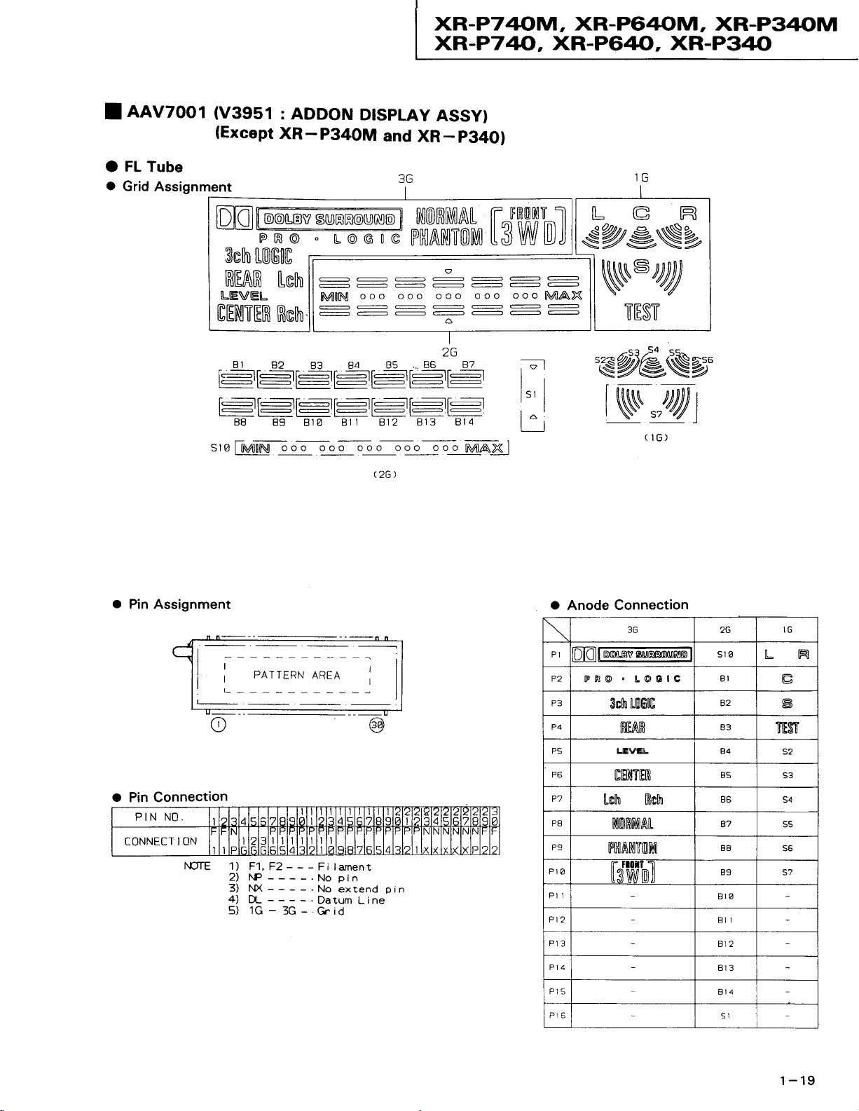
lnvzool
I
FL Tube
O
o
Grid Assignment
(v3951
(Except
: ADDoN
DtspLAy
XR-P34OM
and
XR_P34O)
Assyl
EG@$0RM4t"F"rflRHT^l
P
R
@
3ah
t0G[G
REAR
LEVEL
CIENTER
81
r-a-r-F-
B8
srafN40N
Lah
Rah
82
89
oo-o ooo ooo ooo
L @M
N4[SU
84
83
B1A 81
ooo
1
PHANTOM
ooo ooo
I
,.,86
85
Bl 3 814
812
ooo
(2G)
ILSJ \U\V
ooo
87
N4AXJ
UJJJ
ooo
NI]AX
E
IU
I
l-! tlg lr-{
szsNz
=]
ll Il{tn[( s rllltl)
ll \\\\\\N
\""
'll
a///////
'///
II TEST
e4@Nz
lN-/11
(G)
o
Pin Assignment
Pin Connection
NPTE
, PAIIFRN ARFA
r-l
L--_
o
1) Fl,
F2---Filament
3G
-No
-
No
-Datum
-
Grid
2) NP
3) NX
4)
D_
)) tu
-
I
@
pin
extend p i n
Line
o
Anode Connection
3G
PI
Aru@tvsunts@umo
P2
PR@. [.OG0C
P3
P4
P5 LEVE[- 84
P6
P7
P8
PS
P1A
Pt I
Pt2
Pr3
Pt4
Pr5
Pr6
LOGIG
3ch
MEAIR
GENTER
Lah Rah
NOMMAT
PHANTCIM
't
6l
2G
sr€
BI
82
B3
BS
87
B8
B9 s7
Bla
Bt
Br2
8r3
BI
n16)
lIEST
l
IG
s
S2
s4
ss
s6
1-19
Page 20

XR-P7@M,
xR-P7
40, XR-P64(),
1.7
ADJUSTMENTS
XR-P64OM,
XR-P34()
XR-P3@M
1. TUNER
FM Tuner
I
a
Set the mode
a
Connect
Step No.
I
2
3
Nofes.'
o
Before
contact with
o
Make
the wiring
Adjustment
Adjustment
Front
Sencitivity
TUNED
Lighting
adjusting,
indicator adjustments
FM75 Q Anrenna
SECTION
Section
selector to
as shown in
Title
Center
End
IND.
Level
make sure there is
each other first,
Te.minat
FM BAND.
Fig. I
FM SG
(lkHz,
Frequency
(MHz)
98
Non
modulation
98
98
and then make
in order of AM
1.
t
75kHz dev.)
Level
(dBpV)
80 or
more
l0- 30
lfi.2 98MHz
gap
no
between
adjustments.
-
FM.
Reception
Frequency
Display
98MHz
Adjustment
Location
L6207
L6102
T6101
vR6201
L6101 and L6102.
Adjust
and Pin 28
Adjust so
IC6201
level.
Adjust
IND. start
If there is
Specifications
so that the DC voltage
of IC6201 becomes
that the DC voltage of
(S-meter)
so that the indicators
gap
a
becomes at maximum
to light up.
between them,
la;?n1
IC5201
befween
ot TUNED
bing them into
Pin 4
0Vt50mV.
the Pin12 of
AM
I
a
a
Step
Note.'
a
Tuner
Set
the mode selector
Conoect the wiring
Adjustment
No.
TUNED
I
Lightirg
When SD
and YPW type is
Section
as shown
Title
IND.
Level
to AM
AM SG
Frequency
A M
XR_P74OM,
xR-P740,
Fig.
1- 1 FM Adjustmont
BAND.
in Fig. I 2.
(400H2,
(kHz)
999
used, set
An renna Ter.m
3070 Mod.)
Level
(dBpY,h)
47 !2
the AM Irequency
Loop Antenna
AM
XR_P54OM,
XR-P640.
Connection Diagram
Reception
Frequency
Display
999kHz
step to 10kHz.
r na l
XR_P74OM,
xR-P740,
XR_P
34M
XR-P340
Adjustment
Location
vR6202
XR_P64OM,
xR-P54
Adjust
so that the indicators
IND. start
0. XR-P340
to light up.
X R_P
VOLTMETER
DC
Specifications
34M
of TUNED
1-20
Fig,
1-2 AM
IMW)
Adjuslment
Connection Diagram
Page 21

FM/AM TUNER MODULE
Fig. 1
XR-P74OM.
xR.-P7 4o-,
-3
Adjustment Points
XR-P64OM,
XR-P64HJ_,
XR.P34OM
XR-P340
2.
POWER AMP
1.
Handling Precautions
o
Since
the heat sink and transistor metallic
MODULE SECTTON
nected to the Front Amp
contact the
o
Since there is residual
Module Assy
+B2
(REAR,
power
is
OFF, caution should be
the voltage should
a
When handling the Power Amp
you
do not
Front Amp
I
itep Measurement
I
2
3
Lch side
(chassis)
GND
high voltage in the Power Amp
+31
(FRONT
PWR, PRTEC ASSY)
be discharged).
touch the fan motor
(FRONT
Side
Short both sides of
Insert a resistor
CN7502 *81
Short both sides of C7524.
Turn
voltage in
(Refer
parts
are con-
output, make sure they do not
or other circuits.
ASSY FOR 100W)
even when the
exercised.
Module Assy, make
blade.
ASSY FOR 1OOW)
C7L23 afi C7L24 on the Rear Amp
(0.220,
-81)
the
(or
power
Step 2.
line
ON, wait 6
(If
3W or more) in series
and
necessary,
sure
Item
(terminal
seconds, and then measure
No.
to
5 or 6).
Fig. 2-1.1
2. Adjustment
o
Basically,
replacing a
transistor,
Power Amp
o
Make sure
measuring
same
as room temperature; 25oC is
o
Idle
current stipulated value:
side. Do not operate the Rear
in the connector
(Refer
to FiS.2-2.\
the resistance
and Confirmation of ldle Current
the idle crurent needs to be confirmed
power
transistor,
or when the entire split board Assy
Module Assy has been replaced.
the heat sink has cooled sufficiently
the idle current.
For measuring
resistor
Do not operate Rch
Lch Idle
driver transistor, or bias
(Temperature
should
ideal, if
possible.)
3-50mA.
Remarks
Amp side.
voltage
at both sides of
side.
current l:V/0.22
(0)
when
of the
before
be the
5
Rch side
6
8 Lch
I
side Short between
Rch side Short
10
NOTE:
If
the idle current is
sistor
base, and confirm that
o
Same as Steps
.
Short both sides otC7523.
Turn the
measure
If the
ing
After
firm
power
ON under the above conditions,
the resistance voltage in
measured idle current is
procedure.
the Point A
between the Point B
performing
that it is below 50mA.
below 3mA, support
the idle cunent is within
1 and 2 above.
Step 2.
greater
than 50mA,
pattern
in Fig. 2-3
pattern
in
Fig. 2-3 using solder.
Steps 8 and 9, remeasure
a resistor
(33kQ)
between the emitter and
3-50mA.
and after 6 seconds
perform
using solder.
the idle current
the follow-
and con-
the
Do not
operate Lch side.
Connect
cuit.
Connect R7518
cuit.
Q7501
R7517
(Lch)
to R7515 in a
to R7516 in a oarallel cir-
Q7502
(Rch)
and
parallel
bias tran-
1-21
cir-
Page 22

XR-e2461y1,
)(R-P7
Q,
XR-P64O,
XR-P640M, XR-P34()M
XR-P34O
Rear Amp Side
!
Step Measurement
1
2
Center amp side
(REAR,
PWR,
Short
both sides of C7523 and C7524 orr the Front Amp
Insert a resistor
CN7102 +B2
PRTEC ASSY)
(0.220.
(or
2W or more) in series in the conDector
(terminal
82)
line
Item Remarks
not
operate the Front
For measuring voltage at both sides of
resistor
No. 5 or 6).
side. Do
(Refer
to Fig. 2-4.)
Amp
3 Short both sides of C7124 on the Surround Amo side. Do not operate the Surround Amp.
4
5
Surrould amp side
6
7
C€nter amp side
8
Surround amp side
9
10
Turn
voltage in
a
a
Turn the
seconds measure the resistance
If the
ing
Short b€tween the Point
Short between the Point D
AJter
firm that it is below 50m-{.
power
the
Same as Steps I and 2 above.
Short both sides of C7123 on Surround Amo side.
measured idle current is
procedure.
performing
ON, wait 6 seconds, and then measurc the resistance
2.
Step
power
ON under the conditions in Steps I and 2, and alter 6
Steps 8 and 9, remeasure the idle current and con-
pattem
C
pattern
voltage
greater
than 50mA,
in Fig. 2 5 using solder.
in Fig.2 5 using solder.
in Step
2.
perform
the follow-
R7115
(O)
Amp.
in a
Idle current: | = Y10.22
Do not opemte Surround
Connecl R7l17
cult.
Connect R7118 to R7116 in a
cuit.
to
side.
parallel
parallel
cir
cir-
-
NOTE:
If the idle current is below 3mA, support a resistor
ch)
and confirm that the idle current is
base.
3. Adjusting the Operating
This adjustment is necessary
regulator),
Q7301
VR7701 has been
Assy of the Power Amp
Adjustment-Related Cautions
I
a
sure the heat sink has sufficiently cooled
Make
and
Q7302
replaced, or when the entire split board
Module Assy has been replaced.
same as room temperature
a
Once the
power
measurements and adjustments as
too much time is taken, the
rise, and the
measurement
Adiustment
I
1. Connect a
IC7702 terminals
measurements will deviate
point.)
voltmeter between TEMP and TP
No.3 and 2).
2-6.)
2. Determine the
fan motor operating temperature
by means of the following
t30mV.)
-
Formula:
(85oC
Ta)
Ta: ambient lemp€rature
3. Adjust VR7701 so that the
TP is the value obtained
For examole:
when the room temperature
set value : 185 - 25)
=
't
1140mV
-22
{tolerance
(temperature
Ta.)
has been turned ON, make
heat sink temperature will
formula.
(mV)
x
19
("C)
voltage between TEMP and
from the above Iormula.
is 25oC,
x
19
{mV}
Temperature Setting
when IC7403
quickly
(Refer
within t3OmV).
within
sensors), or
possible,
as
from
(or
to Figs. 2 3
(Tolerance
(15kQ
)
3-50mA.
(+12V
(is
the
Ta
the
between
and
setting
is within
between
of the
(If
the emitter and the
Fan Motor
(VR77O1l
Q7101
(Center-ch)
FROIT ASSY FOR l OOW
FAN
+12V
R7708
R7749
R771 0
R771 1
VR7
701
@
Fig. 2-6 Adjustmenl of Opersting
Motor
Q7102
(Surround-
and
Temperatur€ Setting
ot Fan
Page 23

XR-P74O/M.
xR-P7
4o^,
XR-P6,4{J-, XR-P34()
XR-P64OM.
XR-P34OM
FRONT
REAR,
Point
@
ASSY FOR
PWR,
PRTEC
Fig.
2-1 Power
cN7502
-81
+81
Fig.
2-2
l
OOW
ASSY
Amp
(POWER
FRONT
MOD.
ASSY
(Front
(Rear
Module
FlOO+R2O)
Resistor
FOR
lOOW
Amp
Amp
(O.22e,
Side)
Side)
3W
or more)
Point
@
Resistor
Fig.2-4
Point
(O.22A,
@
REAR, PWR,
cN7 1 02
PRTEC ASSY
Point
@
o
gror.;@
o
bi[b'
I;T:"f
r
i
b
rfu3g*
lil
ff*:,*:'"'u
#;
T"*'b8;Il
-Eqg
-ldji
if**
'
"tj
"
b.
.'":
J
?l#i
.:r 6
c)
5
i:'b
o.
o
lI::,:::
J-,*,-j5-:'.=:l
o---------ttlQ,,]762
o--rrrlQTT$z
6
irrrrr-c eFf
Er%i
!
+l
o-
...4
{l'
EJ
o
? r=1.il
l"t..tgl
J
i"
@-atrro-3
o-Jrtrr-o
*"**oLi"Fr,
li t
*,,,,ffi
${1
*-,*
Y
_Rrj.-"3,ii{
o_*.,o1,,:"'l
Lf qq
^ TH
lgrqi
iltE$
l1"i
jj"j
:*=
:H;.*.'lt"$fl'
o-*sr"--c
o_
i_e
q:
- -r ? I
illi
f..Ogf
6-orro:-=
* r
T I
is1
^-'"'1
*'1fl.1*l
dj-
Ll
I
cN7Eo2
=
Fig. 2-3 FRONT
(This
diagram is viewed
ASSY FOR lOOW
from
the
foil
side)
Fig. 2-5 REAR, PWR, PRTEC ASSY
(This
diagram
is
viewed from the foil side)
1-23
Page 24

XR-P74OM,
xR-P7
40, XR-P640,
XR-P64OM,
XR-P34()
XR-P34OM
3. CASSETTE
a
Adjustment
Mechanical
I
a
Set the TAPE
.
Test
tape: STD-301
1 . Tape
No.
Speed Adjustment
Mode Test
DECK
points
and test
Adjustment
function.
sTD-301
1 PLAY
Electrical
!
(Playback:
3kHz)
Adjustment
Check the tollowing
1.
Confirm that the
tape speed adjustment
completed.
2. Clean the heads
and demagnetize
eraser.
3.
Set the measurement level
4.
Use the specified tape for
(A)
side of the test tape.
STD-331E: For
STD-631: Normal
5. Provide
a
o
a
o
6. Adjust
specified.
Tum
7.
specified.
8. Warm up the
In
REC/PLAY
recordingT/playback
ment.
9. Always follon'
Otherwise, a complete
yoursel{
AC millivoltmeter
Low-frequency oscillator
Attenuator
Oscilloscope
both
the DOLBY NR switch
particular,
playback
blank tape
with the foUowing
right
and left channels
unit fgr several minutes
be sure to
mode for
indicated
the
SECTION
points
are
shown in Fig.
(3kHz,
Tape
before
frequency characteristics
30min).
Adjusting
Points
DECK
Unit
vR4111
starting.
them using a head
to 0 dBV = I Vrms.
adjustment. Use the labeled
adjustment
measuring devides:
unless otherwise
off
unless otherwize
before adjustment.
wartn up the unit in
3 to 5 minutes before starting
adjustment
adjustment may not
order.
be achieved.
3-2 and Fig.
Measurement
Points
TAPE
POINT
(AF
CD Assy)
has been
the
adjust-
TEST
(Rch)
3-4.
Adjustment
Press
the PLAY SW
becomes
flutte! level is below
confirm that
Playback
1. Head
2.
Recording Adiustment
1. Bias Oscillation Frequency
2. Recording Level
3. RecordingT/playback
4. ALC
'As
STD-331E,
STD-3318
attention
3010Hza10Hz. Confirm that wow
the reading is within 3010H2 t
Adjustment
Azimuth Adjustment
Playback Level Adjustment
Adjustment
Operation Check
the reference
the recording level will be hfuher
(160nwbz/m).
to the type oI tape used.
Procedure
and adjust so that the reading
(in
0.270
Adjustment.
the reverse direction,
(Decks
(Deck
Frequency Characteristics
recording level is
When adjusting,
I
and ll)
ll)
Adjustment
Remarks
&
60Hz).
250nwb7/m Ior
by 4 dB for
pay
carefull
1-24
3!5H.
6.3kHu
lOtHr
3t5Hr
Fig.
3- 1 STD-331E Test Tape
12. 5
0kHr
SkHr
6.3
2lHz t{0Hz
I25Hr
53Ht
/t0l'L
Page 25

XR-P74OM,
xR-P7 &,
XR-P64(),
XR-P64OM,
XR-P34()
XR-P34OM
notse
Dolby
to.,€s L,cens,rg Coryoration .
'DOLBY'
Labontoies Lrcensng Corpotation
rcductrcn
and lhe double-D symbol
manufacturcd undet
o
Fig. 3-2
Head Azimuth Adjustment
ltcense
cn arc tadematks of
.
(ol
ion Dolby
Labota-
Dolby
PLAY BACK
RECORDING
Fig. 3-3
Frequency Characteristics
Playback Adjustment
O
Head Azimuth Adjustment
1 .
Tape
Step
Selector
Mode
(AUTO)
I NORMAL PLAY
2. Playback Level
Tape
Step
S€lector
(AUTO)
1 NORMAI
Adjustment
Mode
PLAY
Input Signalzl
Test Tape
_331E
STD
tape
test
(Playback:
-
10dB)
Input SignaT
Test Tape
STD 331E
teat lape
(Playback:
0dB)
10kHz,
315H2,
o
This unit is equipped
a
Do not switch between
Adjustidg Points
Deck
Deck
Deck I
Deck II
Head azimuth
I
adjustment
tr
(Fie.3
a
Since this adjustment determines
Adjusting
VR4201
VR4202
VR4203
VR4204
with auto tape selectot.
{orward and reverse
Measurement
TAPE TEST
sclew
Points
2)
(Lch)
(Rch)
(Lch)
(Rch)
(AF
Measurement
TAPE TEST
(AF
Points
POINT
(L,
Rch)
CD Assy)
Points
POINT
(L,
Rch)
CD Assy)
op€ration with the screwdriver
Adjustment
Value
Ma*.
playback
signal
playback
leYel
Dolby
After adjustment,
paint
lock
azimuth adjustment
screw.
NR level,
Adjustrnent
Value
-
i.2 dBV
Remarks
to the head
perform
Remarks
inserted.
apply
it carefully.
1-25
Page 26

XR-P740M,
xR-P7
Q, XR-P64(), XR-P34()
Recording
O
1 . Bias
Oscillation Frequency Adiustment
XR-P64()M,
Adiustmont
XR-P34()M
Step
Selector
Mode
(AUTO)
NORMAL REC
2. Recording Level
Tap€
Step
Tape
Selecto!
(AUTO)
Mode Input Sigrral/Test Tape Adjusting
1 NORMAL REC
2
NORMAL
REC,,
PLAY
Input
Signaf
Test Tape
Load the STD 631
test
tape and set the
recording mode.
Adjustment
Input
a 315H2 signal to the
VIDEOiAUX IN terminal and set
the input selector to VIDEO.
STD 631 test tape and
"playback
record,
signal.
Adjusting Points
Deck
Deck tr
the 315H2
Measuement
Poiots
I
Between
point
in Fig.
3-4 and GND.
Points
Deck
I
Input signal
Deck
II
Deck
I TAPE TEST
Deck tr
level
vR4301
vR4302
(Lch)
(Rch)
Oscillation fre-
quency
@
Measurement
TAPE TEST
(AF
(AF
Adjustment
Value
to be
105.0kH2
t2kHz.
Points
POINT
(L,
Rch)
CD Assy)
POINT
(L,
Rch)
CD Assy)
Remarks
When the
ON while
is depressed, the frequency
will decrease 2
Adjustment
Repeat recording,
and adjustment until
playback
signal becomes 5.2dBV.
pori.er
BAND buttol
the
Value
5.2 dBV
level of the 315H2
is tumed
3 kHz.
Remarks
playback
Recording/playback Frequency
3.
Characteristics Adjustment
Tape
Step
Selector
Mode Input Signal/Test Tape Adjusting Points
(AUTO)
Deck
Deck
Deck
Deck tr
I
II
I
L NORMAL REC
2 NORMAL
REC,,'
PLAY
Input a 315H2 siSnal to the
VIDEO/AUX IN terminal
and set
the input selector to VIDEO.
Load the STD
record/playback
10kHz signals.
below)
-631
test tape and
the 315H2 and
(see
the Note
Note; Set to the same level used for the 315H2 input signal at step 1.
4.
ALC Operation Check
Step Selector
(AUTO)
I
NORMAL
2
Mode Input Signal/Test Tape Adjusting Points
Input siSnal level
Set to a level + 10dB
above the input level at
step 1.
REC
PAUSE
Input a 315H2 signal to the
.
VIDEO/AUX IN
terminal and set
the input selector to VIDEO.
a Since
distortion Irom increasingdue to underbias.
adjustment
this
Measurement
Points
aJfects recording bias,
Adjustment
TAPE TEST
POINT
Input
level
VR4351
VR4352
signal
(I-ch)
(Rch)
(L,
Rch)
(AF
CD Assy)
TAPE TEST
POINT
(L,
Rch)
(AF
CD Assy)
Measutement
Points
Repeat
playback
signal is vrithin 0 t0.5dB
from that of the 315H2
signal.
TAPE TEST
POINT
(L,
Rch)
(AF
CD Assy)
Value
25.2 dBy
adjustment until
level of the 10kHz
Adjustment
Value
-5.2
dBV
2.h.2.5d8y
prevent
Remarks
Remarks
1- 26
Page 27

XR-P74o/M,
xR-P7 4o^, XR-P6,40^,
XR-P64()M,
XR-P340
XR-P34()M
Left Side
DECK
Unit
4. DOLBY PRO.LOGIC
ADJUSTMENT
Cassette
Fig.
3-4
Right
Side
vR41
1
1
vR4301
vR4302
vR4352
Mecha
vR4351
DECK
Unit
Adjusting Points and Measurement
DOLBY
5.
Points
SURROUND ADJUSTMENT
1. Turn FUNCTION
LOGIC,
2. Input
Terminal
180o inverse
Adjust
3.
and CENTER MODE
a IkHz sine wave
(L/R). (But
of the input signal for
VR3401
so that the Dolby
300mVrms.
NOTE:
Wait
before
least
at
making
2 minutes
adjustments.
,PROLOGIC
to VIDEO,
the
after the
assy
MODE to PRO-
to NORMAL.
(253mVrms)
input
signal for R should
L.)
Test Point
power
has been turned
to the
(CN3402)
Front
Video
be
ON
1. Turn
2. Input
3. Adjust VR3401
is
FUNCTION
a LkHz sine wave
Terminal
(L/R). (But
180" inverse
7lmVrms.
to VIDEO and SURROUND to
(260mVrms)
the input signal for
of the input signal for L.)
so that the Dolby Test Point
to the
R should
(R3440)
ON.
Video
be
is
NOTE:
--_
::
-^-^
-^--
o
|
o-,'r{
ltllC
power
e**9o-a
?
...i
f. I
!
i i i
..Od
@!
-
-f,
o-rrr.
o-'r" <
oo o: p
oa
o;
l-la
El!
u: o)
u: o)
o !!ic
has
been turned ON
o-.r'. <
e'r''n
^p==,;,.i;;J1
,o
A I
a
J lo-Jr.r {
"
:l
iLe
i,,:,.
@^ -
:l
:l
:l.l :
:l.l :
o
o
eo:r-r
eo:r-r
:l
o-,r.. <
front
ororor
::
ol olo
"..1
{o'o:
'o:
o-
€:
$
i
v
x
D
Wait at least 2 minutes
before making
DOL
SURR
o-o
assy
R3440
i Ft*,
(:)E-l
Akl
:
(g'
r
adjustments.
"-"
qi
o
after the
.,1&,
VR34OI
'l^
:;-.o
.'+
;-.8f*.:"
'
:o.:"io'or
|
I
a
:
-3;
-3;
--+-1u3J-A
:"
Dolby noise
tories
Llcensing
"DOLBY"
Laboratories
and
reduction
Corporation
the
Licensing
manufactured
.
double-D
symbol t!
Corporation.
under license
are trademarks
from
Dolbv
of Dotby
Labora.
Manufactured
ratton.
DOLBY and the double-D symbol CE are
tories Licensing Corporation.
under
/icense
from Dolby
Laboratories Licensing
trademarks
of Dolby
Corpo-
Labora-
1-27
Page 28

XR-P740M,
xR-P74{),
XR-P64()M,
XR-P34()M
XR-P64(), XR-P34()
6. CD SECTION
Adiustment Methods
I
If
aU wrong with the
a Adjustment ltems/Vefitication ltems
If the specified values cannot
described in steps 1-4, the
player
a disc
Step
1 Focus offset verification TPl, Pin6
2 Tracking error balance verification TPl, Pin2
Pickup radial/tangential
3
adjustment
RF level
Focus servo loop
{FOR
is
adjusted incorrectly or inadequately, it may
pickup
veriJication
CD MULTI AND
or the circuitry. Adjust correctly
be obtained or no adjustment is
pickup
block may be defective.
Item
direction tilt
gain
adiustment
CD SINGLE)
and Order
malfunction or not work at all even though tlere is nothing at
foUowirg the adjustment
possible
Test Point Adiustment Location
(FOER)
(TRER)
TP1, Pinl
TPl, Pinl
TP1, Pin5
TP1, Pin6
(RF)
(RF)
(FOIN)
(FOER)
performing
by
procedure.
verifications
the
None
None
Radial tilt adjustment screw,
Tangential titt adjustment screv/
None
VR8152
(FCS
GAN)
or adjustments
6 Tracking servo loop
Abbreviation Table
O
FOER :Focus Error
TRER : Tracking Error
FCS GAN : Focus Gain
TRK GAN : Tracking Gain
FOIN
TRIN
Measuring Instruments and Tools
O
1. Dual trace oscilloscope
2. Low-frequency oscillator
3. Test disc ffEDS-Z)
4. Low
Resistor
5.
6. 8cm disc
7. Ball
8. Standard tools
: Focus In
: Tracking In
pass
filter
(100kO)
(With
point
hexagon
(39kO
at
gain
adjustment
(10
probe)
:
I
+ 0.0019F)
least about 20 minutes oI recording)
wrench
(GGK1002)
TPl, Pin3
TPl, Pin2
(TRIN)
(TRER)
VR8151
(TRK
GAN)
1-28
Page 29

Test Point
O
and Adjustment
XR-P740M,
xR-P740,
Variable Resistor
XR-P640M, XR-P340M
XR-P64{J_, XR-P34()
Positions
DISPLAY
Notes
O
1. Use a 10 :
2.
All the knob
Assy
probe
1
positions (settings)
for
the oscilloscope.
Fig. 1 Adjustment
for
the oscilloscope in
\t/
ooo
the adjustment
vR81s2
[a]
Location
/\
procedures
are for when
a 10 : 1
probe
is
used.
Test
O
These
these models
carried
mode.
How
1. When
2.
When the test mode
If
Mode
models have
are
out by operating
lSetting
these
to set this model
the Power
Short-circuit
the display is still
a test mode so
in
test mode,
these keys with
models to
switch to activated,
between both
is set correctly,
the same as
test model
into test mode.
that the adjustment
the keys on the
the correct
set the FUNCTION
CD TEST
usual, test mode
points.
the display
and checks required
panel
front
(See
is different from
work
procedure.
Fig. 1)
has not been
for service
differently from normal.
For
these models, all adjustments
button
to CD.
vrhat it usually
set correctly, so repeat
is when the
carried
can be
Adjustments and
power
Steps 1-2.
out easily.
are carried out in
is
When
checks can be
test
turned
1-29
Page 30

XR-P74OM, XR-P64OM, XR-P34OM
xR-P7
4,
XR-P64(),
XR-P34()
lRelease
Here
1. Press the STOP key and stop all operations.
2. Tum off the
loperations
Code Key Name Function in Test Mode Explanation
>/:l
from test model
procedure
is
the
of the keys in
DOLBY
for releasing the test mode:
pov/er
switch on
NR
the
test model
Focus servo close The laser
front
PLAY//PAUSE Spindle servo ON
panel.
is lit up and the focus actuator is lifted up,
diode
then lowered slowly and
point
where the objective
With the
disc by hand,
If
correctly. If
laser diode
the actuator is
to its original
Starts the spindle motor in the clockwise direction and
the disc rotation reaches the
500rpm
closed loop.
Be careful. Plessing
makes the
If the focus servo does not
the laser light shines on the mirror section
periphery
player
in this state,
you
you
can hear this sound, the focus servo is operating
you press
lights up, the focus actuator is
lowered and raised three times and returned
position.
at the inner
spindle motor run at the maximum speed,
of
disc, the same symptom is occurred.
the
the focus servo is closed at the
lens is focused on the disc.
you
if
cao hear the
this key with no disc mounted,
prescribed
periphery),
this key when there is no disc mounted
go
correctly
lightly rotate the
sound the focus servo.
pulled
speed
sets the spindle
into a closed loop or
at the outermost
stopped
up, then
(about
servo in a
the
when
1-30
Tracking servo
close,,'open
Pressing this key
operating correctly
into a closed loop, displays
back and the elapsed time
playback
the
If the elapsed time is not displayed or
or the audio
is shining on the section with no sound recorded
laser
outer edge of the
or that there is some other
This key is a toggle
alternately. This
when the focus servo and spindle servo are
in closed loops
the track number being
on the front
signal.
played
is not
disc, that something is out of adjustment,
key has no elfect if no disc is mounted.
back correctly,
problem.
key
and
puts
the tracking
panel,
not counted correctly
it may
open/close the tracking servo
servo
played
and outputs
that the
be
at
the
Page 31

XR-P740M, XR-P640M, XR-P34()M
xR.-P7 40, XR-P64(),
XR-P340
Code Key Name Function
Lr<<
MANUAL//
TRACK
SEARCH
Carriage reverse
(inwards)
REV
MANUAI-//
TRACK
Caniage
(outwards)
SEARCH
FWD
STOP Stop
E
EJECT CD
A
magaz ine eiect
(For
CD
in Test Mode Explanation
forward
Multi)
Moves the
disc. When this key
closed loop, the tracking
open loop, Sitrce the motor does
tlre mechanical end
operation.
Moves the
disc. When this key is
closed
open loop. Since the
the mechanical end
operahon.
Initializes and the disc rotation stops.
The
oressed.
Stores Disc I in the CD magazine, then ejects the CD
magazine. However, even tlough the CD magazine is
ejected,
Eveo if the CD magazine
remains where
pickup position
position
pickup
loop,
pickup
the
tracking servo automatically
the
and disc remain where they are when this key is
pickup
it is.
toward the inner diameter o{ the
pressed
is
point
pressed
motor does not automatically stop at
point
does not return to the
with the tracking servo in a
servo automatically
in test mode, be
tov/ard the outer diameter of the
with the tracking servo
in test mode, be careful with this
is mounted
goes
into an
not automatically stop at
careful
park position.
again, the
goes
pickup
with this
in
into an
a
OPEN/,CLOSE Disc tray open,,'close
A
Note: When inserting
playback
to
lHow
In test mode, since
correct order to close
Here is
DOLBY
I
the
key
operation sequence for
NR
0
i-- mr I
+
t r'- r.--l
Open/close the disc tray. This key is a toggle key and
(For
CD Single)
the magazine, disc 7 of the
a disc
in
servos operate independently,
the
the servos.
Lights up the laser diode and closes the focus servo.
Starts the
Closes the tracking
model
test
playing
spindle motor
servo.
magazine is
back a disc in test mode.
and closes
open/close
Pressing this key when the disc
then opens the tray.
This key operation does not affect the
pickup.
loaded automatically.
playing
the spindle servo.
back a disc
tray altenately.
requires
that
is
turning
you
stops
position
operate
the disc,
of the
the keys in the
Wait at least 2-3 seconds between each of these operations.
t-Jl
Page 32

XR-P740M,
xR-P7
&,
XR-P64()M,
XR-P64(),
XR-P340M
XR-P34()
Focus
I
.
Objective
a
Symptom when out
of adjustment
a
Measurement
Instrument
Connections
IProcedurel
Verify the DC voltage
Note: If the specified values
Tracking Error Balance Verification
I
.
Objective
Offset Verilication
Verify
The
Connect the oscilloscope
TPl, Pin6
[Settings]
at TPl,
or adjustments
described in adjustment items 1-4, the
To verify
the DC offset for the focus
model does not focus in
(FOER)
SmVldivision
l0ms7/division
DC mode
Pin6 FOER) is 0tsOmV.
cannot be obtained or no adjustment
that there
error amp.
and the RF sigaal is dirty.
to
is
no variation in the sensitivity of the tracking
a
Player
a
Adjustment
a
Disc
State
is
pickup
Location
possible
by
block may be defective.
Test mode, stopped
(just
None
None needed
pertorming
the
photo
Power
switch on)
the veifications
diode.
a
Symptom
of adjustment
a
Measurement
Instrument
Connections
lProcedurel
1. Move
key or REV
2. Press the DOLBY NR key, then
serYo.
3. Line up the bright line
4. Supposing that the
is
When
When
when
out
Play does not start or track search is impossible.
Connect the
TPl,
connection may be Yia a low
pass
[Settings]
(B).
the
the
pickup
to midway
i{<1
following
.
<l{
(ground)
positive
expression is satisfied.
o=t,+']=o.r
A.B,
?']so.r
Pin2
filter.
across the disc
key.
amplitude of the trackiqg error signal at TP1,
a
oscilloscope to
(TRER).
50mV7/division
5ms7/division
DC mode
the
at the center of the oscilloscope screen and
This
(R:35mm)
PLAY7/PAUSE
Player
State
a
Adjustment Location
a
Disc
with the MANUALz/TRACK SEARCH FWD
key in that order to close the focus servo then the spindle
Futl
pin2
Test mode, focus and spindle
servos closed
open.
None
and tracking
YEDS_7
put
the oscilloscope into DC mode,
(TRER)
(A)
is
and the negatiye amplitude
servo
>>. >>l
When lhsrg
compon€nt
is
a DC
thero is no
Whon
componenr
DC
Page 33
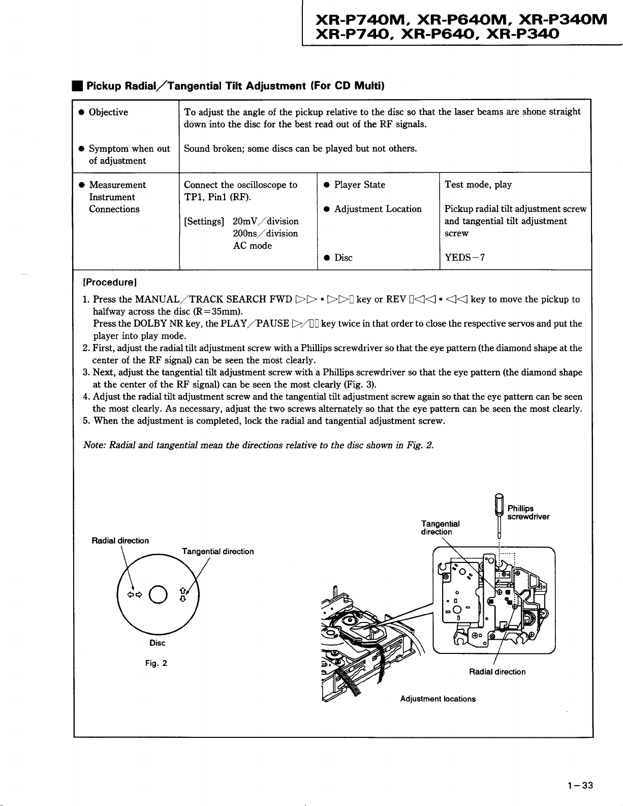
XR-P740M,
xR-P7 40,
XR-P640M, XR-P34()M
XR-P64{J_, XR-P340
Pickup Radlal/Tangential Titt Adjustmont
!
a
Objective
o
Symptom
of adjustment
o
Measurement
Instrument
when out
To adjust t}te angle of the
down into
Sound broken; some discs can be
Connect the oscilloscope
TP1, Pinl
disc for the best read out of the RF signals.
the
(RF).
Connections
[Settings]
20mV/division
200ns7ldivision
AC mode
pickup
to
(For
o
o
o
Multil
GD
relative to the disc so that
played
Player State
Adjustment Location
not others.
but
Disc
the laser beams are
Test mode,
Pickup radial tilt adjustment screw
and tangential tilt adjustment
screw
YEDS-7
lProcedurel
1.PresstheMANUAL/TRACKSEARcHFwD>>.>>!keyorREv|<<.<<
halfway across the disc
Press the DOLBY NR key, thePLAY/PAUSE
player
2. First, adjust the radid tilt adjustment screw with a Phillips screwdriver so that the eye
center of the RF signal) can be seen the most clearly.
3. Next, adjust the tangential tilt adjustment screw with a
at the center of the RF signal) can be seen the most clearly
4. Adjust the radial tilt adjustment screw and the tangential tilt adjustment screw
the most clearly. As necessary, adjust the two screws alternately so that the eye
5. When the adjustment is completed, lock
into
play
mode.
(R:35mm).
the
>/|,key
radial
and tangential adjustment screw.
twice in that order to close the respective servos and
Phillips
screv/driver so that the eye
(Fig.
3).
again
pattern
pattern
so that the
shone
straight
play
put
the
(the
diamond shape at
eye
(the
diamond shape
pattern
can
pattern
can be seen the most clearly.
the
be seen
Note: Radial and tangential mean
Radial direction
Tangential
d"O
Fig.2
I
Disc
directions relative
the
direction
to the disc shown
in Fig. 2.
1-33
Page 34

XR-P740M, XR-P64()M, XR-PS4()M
xR-P74(), XR-P64trJ_, XR-P340
Pictup Radial/Tangential Tilt Adjustment
I
o
Objective
o
Symptom
of adjustment
Measurement
Instrument
Connections
when out
To
adjust the angle of the
down into the disc for the best
Sound broken; some discs can be
Connect the oscilloscope to
TP1,
[Settings]
(RF).
Pinl
2OmV division
20Ons7ldivision
AC mode
(For
pickup
read
Single)
GD
relative
out of
played
O
Player State
o
Adjustment Location
o
Disc
the disc so that
to
the RF signals.
but not others.
the
Test mode,
Pickup radial tilt adjustment
and tangential tilt adjustment
screw
8 cm disc
[Hewever,
min of audio signal
lProcedurel
l.PresstheMANUAL/TRACKSEARCHFwD>>.>>!keyorREV[<<.<<
external
Press the DOLBY
player
2. First, adjust the
shape at the
Next, adjust the tangential
3.
diamond shape at
X
4. Adjust the radial tilt
the most clearly.
5. When the adjustment
circumference of the disc.
NR key, thePLAY
play
into
The ball-point
used.
mode.
radial tilt adjustment
center of the RF signal)
the center of the
type hexagonal
adjustment screw
As necessary, adjust the
tilt adjustment
wrench is used because
is completed,
/PAUSE
screw with the hexagon wrench
can be seen the
RF signal) can be seen the
and the tangential tilt
lock the radial and tangential
>/alkey
screw with the
two screws alternately
twice
most clearly.
hexagon wrench
most clearly
the disc will
adjustment screw again
in
order to close the
that
(GGK1002)
(GGK1002)
(Fig.
get
in the way
so that the eye
adjustment
so that the eye
3).
so that the eye
pattern
screw.
laser
respective servos and
so that the eye
if a normal hexagonal wrench
can be seen
are shone straight
beams
play
those
pattern
pattern
screw
with approx.
(music).1
put
(the
diamond
pattern
the most clearly.
(the
can be seen
20
the
is
Note:
-34
1
Radial and tangential
direction
Radial
J"o
Disc
Fig.2
mean the directions
Tangential
direction
3
relative to the
disc shown in
Fig. 2.
direction
Tangential
direction
Page 35

Out ol adiustment
XR-P740M,
xIl.-P7
Optimum adiustment
40, XR-P64(), XR-P340
I
tl
.t l,
XR-P64()M,
of adiustment
Out
,//A r,
u// vI
XR-P34()M
RF Level Verification
I
o
Objective
o
Symptom when out
of adjustment
Measurement
Instrument
Connections
To verify
play
No
Connect the oscilloscope to
TPl, Pinl
ISettings]
playback
the
no
or
search
(RF).
50mV
10ms/division
AC mode
RF signal amplitude.
division
W
Out of
adiustment
Fig. 3 Eye Pattern
o
Player State
o
Adjustment Location
o
Disc
I
Optimum
adiustment
Mil\
Out of
adjustment
Test
mode,
None
YEDS-7
play
lProcedurel
or
pickup
REV
to midway across the disc
!<<
1.
Move the
key
close the respective servos
2.Yerify the RF signal
(R:35mm)
put
and
amplitude is 1.2Vp-p+0.2V.
the
player
into
with the MANUAL/TRACK SEARCH FWD
play
mode.
>> . >>!
1-35
Page 36

)(F..P74(,.M.
xR-P74(),
XR-P64{J--,
XR-P64OM,
XR-P34O
XR-P34OM
Focus
!
o
Objective
o
Symptom
of
o
Measurement
Instrument
Connections
Servo
when
adjustment
Loop
out
Gain
Adjustment
To optimize
Playback
See Fig. 4.
ISettings]
does not start
the focus
servo
or focus
loop
gain.
actuator
o
Player
o
Adjustment
noisy.
State
Location
Test mode,
vR8152
cHl
20mY/division
X-Y mode
a
Disc
YEDS-7
CHz
5mVzldivision
lProcedurel
1.
Set the AF
generator
output
to t.2kLlz
and lVp-p.
2.PresstheMANUAL/TRACKSEARcHFwD>>.>>!keyorREV!<<.<<
halfway
to close the corresponding
3. Adjust VR8152
across the disc
(FCS
(R:35mm),
servos
GAN) so
that the Lissajous
then
and
press
put
t}re DOLBY NR
player
the
into
waveform is
key, thePLAY
play
mode.
symmetrical
/PAUSE
about the X axis
>/D]key
play
(FCS
GAN)
twice in
and the Y axis.
that order
Focus
Gain
Higher
Pin5
Pin4
Pin6
Adjustment
gain
{FOIN}
(GND)
(FOER)
1.2kHz
1 Vp-p
Fis. 4
ffi
Optimum gain
(10:1)
ffi,
gain
Lower
1-36
Page 37

xR-P7 4oM, XR-P64{)M,
xR-P7 4{), XR-P64{),
XR-P340
XR-P34()M
Tracking
I
o
Objective
O
Symptom when out
of adjustment
o
Measurement
Servo
Loop
Gain Adjustment
To optimize the tracking servo loop
Playback
does
not
start, during searches the actuator is noisy, or tracks
See Fig. 5.
o
Player
gain.
State
Test mode,
Instrument
Connections
ISettings]
o
Adjustment Location
vR8151
CH1
50mVzldivision
X-Y
mode
o
Disc
YEDS_7
CHz
20mVzldivision
lProcedurel
1.
Set the AF
generator
output to l.2kHz
and
2Vp-p.
2.PresstheMANUAL/TRACKSEARcHFwD>>.>>!keyorREV!<<.<<
halfway across the di5g
to close the corresponding
3. Adjust VR8151
(TRK
(ft:35mm),
servos and
GAN) so that the Lissajous waveform is symmetrical
then
put
press
the DOLBY NR key,
player
the
into
play
mode.
(10:
thePLAY
1)
/PAUSE
about the X axis and the Y axis.
>/llkey
are skipped.
play
(TRK
GAN)
twice in that order
Tracking
Pin3
Pin4
Pin2
Gain Adjustment
(TRIN)
(GND)
(TRER)
0.001
pass
Low
uF
filter
(10:
t1
1.2kHz
2VP-P
Fis.
ffi
Higher
gain
Optimum
gain
Lower
gain
1-37
Page 38

XR-P74()M,
xR-P7
NOTES
a
c
c
(1I
4, XR-P64(),
1.8
PARTS
;
Parts mafued
The
mark found
A
be
swe to use
Paxs
marked
PACKING
XR-P640M,
"NSP'
by
parts
by"Q'
LIST
on some
of
FOR
generally
are
component
identical
ate not always
XR-P340M
XR-P340
PACKING
,navailabre
parts
indicates
designation.
kept
in stock.
AND
because
t]1ey
the imNrtance
Their delivery
EXPLODED
are not in
ow Master
of the safety
time
may be longer
factor oI
VIEWS
parts
spare
the
than
usual or
part.
List.
Therefore,
they may
when
replacing,
be unavaihble.
1. FOR
{1)-
For
!
Ma.* ilo.
I
Part
XR
XR-P7z10M/SD
1
2
3
4
6
7
8
9
10
11
For
XR-P74OM/YPW,
number
_
P74OM/SD
Mark
XR-p740M,
Dascription
MAGAZINE
OPERATING
(ECS-
1,2,3/SA4)
REMOTE
(cu-xRo12)
BATTERY
FM ANTENNA
LOOP ANTENNA
FRONT PAD
REAR
PAD LR
PACKING
SHEET
differs between
No.
ASSY
INSTRUCT]ONS
CONTROL
COVER
(L8043)
LR
CASE
Symbol
& Do3cription
XR-p7zto,
UNIT
XR-P7zrO/SD,
-
XR
P74OM/YPW,
XR-p6rroM
parts
No,
PXA1s49
ARC7006
AXD7007
Az.47032
ADH1O16
ATB1O12
AHATOO4
AHATOO5
AHD7O39
AHGTOO4
XR-P64OM/SD.
SD
-
XR
xR-P740M
YPW
AND
XR_p640
p74OlSD,
XB-
YPW
and XR-P64O/SD
XR-P64OM/SD,
P.n
I{o.
P7lu)
SD
xR- P640M
SD
YPW, XR
xR-P640
YPW
-
P640/SD
SD
and
Romarks
r
-38
Operating instructions
(English/Spanish/Chinese)
Operating instructions
(English)
to
P€cking
Remote control
csse
{cu-xRo12)
1
Romote
{cu
Msgazin€
control unit
-xFo10)
assy
unit
ARC7006
AHD7O39
AXDTOOT
PXAl
549
ARBTOO6
AHD7O39
AXDTOOT
PXAl549
ARC7006
AHD7O38
AXDTOOT
ARC7006
ARBTOO6
^1"1::'
iT-1":'
AXDTOO2
PXA1549
AXDTOO2
PXA1549
ARC7006
iT-1":'
AXD7002
Page 39

XR-P74()M,
xB.P7 &,
XR-P64()M,
XR-P64(),
XR-P340M
XR-P340
lll-2.
I
Mark [tlo. D$crlption
I
Part number differs
FOR XR-P3rtOM
For XR-P3zl0M/KU
MAGMINE ASSY
I
2
OPERATING
(E
1, 2,3/S/M)
REMOTE CONTROL
3
(cu
xR009)
BATTERY COVER
5
FM ANTENNA
6
7
LOOP ANTENNA
8
FRONT PAD
REAR PAD LR
9
10
PACKING CASE
11
SHEET
For XR-P3z[OM/KC,
between XR-P34OM/KC,
M.rk No. Symbol &
AND XR-P3rtO
INSTRUCTIONS
UNIT
(L8043)
LR
SD, YPW,
Dcacriptlon
No.
Parts
PXAl549
ARBTOO6
AXD7001
MA703r
ADHlOT6
ATB1O12
AHATOO2
AHATOO3
AHD7O35
AHGTOO3
XR-P34O/SD and
SD, YPW,
xR
KU
KC SD
YPW
XR-P34O/SD, YPW and
Pln No.
-
P3/OM xF- P3/ro
YPW SD YPIV
XR-P340M/KU
Rcmark3
Operating
(English)
Operating
(English/Spanish/Chinese)
Operating
(French)
10
Packing case
I
Magazine assy
instructions
instructions
instructions
ARBTOO6
AHD7O35
PXA1549
AR87006
ARC7007
AHD7O35
PXA1549
ARC7006
AHD7O34
PXA1549
ARBTO06
AHD7O34
PXA'I549
ARBT006
ARC7006
AHD7O33 AHD7O33
1-39
Page 40

XR-P74OM, XR-P64OM, XR-P34OM
xR.-P7 N, XR-P64(), XR-P34()
(2I
EXPLODED VIEWS
(21-
1. EXTERIOR
For XR-P7zlOM, XR-P74O,
I
For XR-P7zOM/SD
O
Mark l{o.
Doscription
XR-P6rtOM and XR-P640
Parts No. Mark
Doscrlption
o.
Pans No.
A
A
A
NSP
A
NSP
POWER TRANSFORMER
1
(T8005)
2 FUSE
3
4 STRAIN RELIEF
5 GROUND
6
7 MULTI MECHA
8 CASSETTE
9 CHASSIS
10 REAR
11
12
t7
18
19
20
2l
22
23
24
25
26
28
29
30
("t2.5N250V,
AC POWER CORD
LEAD
FLEXIBLE CABLE
MOD. BC
PANEL
RUBBER
TRANS FRAME
BRACKET
NYLON BINDER
PCB SPACER
PCB CONNECTOR
FRONT PANEL
TUNER PLATE
DOLBY PLATE
DECK
JOG
VOL KNOB
BALANCE
P. BASS KNOB
BONNET
AF CD
VR ASSY
H. P ASSY
SHEET
PI.ATE LR
KNOB
KNOB
ASSY
(3
x
ASSY
FU1)
01)
ASSY
12)
(PVC)
ATS7O15
AEK_512
ADG1O51
AEC-882
ADBlOOl
ADD1127
AXA7006
EXK2420
ANATOOl
ANC7036
AEB1111
ANATOO2
ANGTOO2
AEC-093
AECI372
AEC1500
AMB7084
AAK7O12
AAK7O13
AAK7O18
AABTOO6
AAB7O21
AABTOO8
AAB7O13
ANETOOS
AWZ?095
AW27282
AW27t05
46
47
48
49
50
52
54
56
58
59
60
62
64
66
68
NSP7172
SCREW
FRONT PANEL A
LENS
AMP. TUNER
DOOR L
DOOR
CATCHER
DOOR SPRING
SPRING
DOOR
DECK. CD
M_CD PANEL
DAMPER
KEEP PI.ATE
FRONT PANEL
DOLBY BUTTON
LEVEL BUTTON
DOOR SHAFT
DAMPER
DOOR SPRING
MULTI BUTTON
MULTI DOOR
LOCK LEVER
SCREW
VOLTAGE SELECTOR
(T2.5A./250V,
FUSE
GROUND LEAD
PAXATLEL
R
BUT-TON
ASSY
WIRE
BUTTON
(L)
(R)
B
SPRING
FU2)
02)
vPz30P080FzK
AMB7O59
(S8OO1)
AAK7O21
AAD7O48
AAN7016
AANTO2O
AEC7001
ABHTOOl
ABHTOO2
AAD7049
AAK7O16
AXA7001
ABK1O17
AMB7067
AADTOOT
AAD7012
AXA7003
PXA1484
ABHTOO3
AADTO09
AAK7O17
ABHTOO4
BPZ2OPOSOFMC
507
AXX
AEK-512
ADBlOO5
D20PyY0615E
32
33
u
36
37
38
39
40
4t scREw
42 SCREW
43
44 SCREW
45 SCREW
1-40
SECONDRY TRANS
DISPLAY ASSY
CD DECK SW
TRANS
PROLOGIC ASSY
ADDON DISPLAY ASSY
FIWAM TUNER
POWER MOD. F100+R20
SCREW
SCREW
PRIMARY ASSY
(P2.6 x
ASSY
ASSY
MODULE
8)
AWZT2rl
AWZ72L5
AWZ7r25
AWZ7t30
AWZ7l38
AW27141
AXQ1012
AXQ1019
ABA1095
ASZ4OPO6OFMC
BBZ3OPO6OFMC
BBZ3OPOSOFZK
BPZ26PO8OFMC
CBZ3OPO8OFMC
Page 41

XR-P721()M, XR-P640M,
xR-P7 &, XR-P64(),
XR-P34()
XR-P340M
For XR-P74OM/YPW.
O
Part number differs between
xR-P74O/SD, XR-P64OM/SD,
XR - P74OM/YPW, XR - P74OISD,
XR - P74OM/SD
Mtrk No, Symbol & Do3criptlon
2a
29
34
36
7
7
69
A
1
A
A
70
A
AF
CD assy
VR assy
DISPLAY
CD
TRANS PRIMABY assy
PROLOGIC assy
DOL SURR assy
ADDON DISPLAY assy
MULTI MECHA assy
SINGLE MECHA assy
58001 Voltage selector
T8OO5 Powertransformer
AC
FU2 Fuse
assy
DECK
Sw assy
power
cord
{T2.5A/2sOV}
-P
XR
740M
SD YPW SD
AWZ7095
AWZ72A2
AWZ1215
AWZ7125
AWZ7130
AWZ7138
AWZ7141
AXATOO6
AKX-507
ATS701 5
ADG1051
AEK_512
AWZ7095
AWZ7282
AWZT 215
AWZ1125
AWZ7127
AWZ7138
awz7141
AXATOO6
aTs7015
ADGl 123
YPW and
XR-P64OM/SD,
Parl No,
XR - P7ltO xR-P640M
XR-P64O/SD
YPW. XR-P640/SD and
SD YPW SD
awz7281
AWZ72a2
awzT
AWZ1124
AWZ7130
AWZ7091
AWZ7099
AWZ71 18
214
awz? 124
AWZ7130
AWZ7091
AWZ7099
AWZ71 18
AWZ7125
AWZ1127
AWZ7138
awz1141
awz1137
AWZ7139
AXATOO6
AWZ7137
AWZ7139
^11'::'
;;,;;.
AKX-
ATS7015
ADG1O51
AEK-512
507
AKX_ 5O7
ATS7013
ADG1051
AEK-512
ATS70l3
i::I:'
xR - P640
AWZ7089
AWZ7099
AWZ71
AWZ7124
AWZ7130
AKX_507
16
AWZ1137
AWZ7139
AXATOO4
ATS70 t 3
AOG't
051
AEK-512
Ramo]ks
: Refer to
X
17
47
59
64
56
66
10
67
71
19
21
42
73
Front
F-
t_
f-
I
f-
Ft^
.
F
lL
R€sr
Multi button
Lock lever spring
Ground lead
Dolby
Tray
Scrgw
(tor
Caution label
page
2-3
panel
assy
panel
Front
FronI
oaner
A
t'
Door spring
Door
shalt
Damper
ucr€w
M-cD
s-co
Danel
panet
t,t,,ni aoo,
panel
plate
cap
CD MECHA assy)
(*3).
AM87084
AMB7O59
AMB7O67
ABHTOO3
AXATOO3
PXA1484
AAK7016
AAK7017
ANC7036
AADTOO9
ABHTOO4
ADBl OO5
AAKTO,I3
BlaJUr"UUUfa[
AMB7O84
AMB7O59
AMB7067
ABHTOO3
AXATOO3
PXA1484
AAK7016
AAK7017
ANC7040
AADTOO9
ABHTOO4
AOB1005
AAK701
uu4Jutuuut{l
vRw-329
3
AMA7083
AMB7O58
AMB7O67
AMB7O82
4M87056
AMB7O65
ABHTOO3
AXATOO3
PXA1484
AAK7016
AMB7O82
AMB7O56
AMB7065
ABHTOO3
AXATOO3
PXA1484
AAK7016
oo.*.ro:'
ANC7035
AAK7013
AAKTO2O
AAK7017
ANC7029
AADTO09
A8H7004
ADBl OO5
AAK7014
AAK7017
ANC7033
AADTOO9
ABHTOO4
ADB IOO5
AAK7O14
uuliurluufwuuz3{jtlJUUr-aiUU4JUTUUUIZI(
vRw-329
AMB7O81
AM87055
AMB7O65
AAK7O53
ANC7028
;;;;;.
AAKTO2O
't-41
Page 42

XR-P74OM.
xR-P7
40, XR-P64(),
XR-P64OM.
XR-P34()
XR-P34OM
For XR
I
-
P3rtOM and
O For XR-P34OM/KU
Mark No. Doscription
A
A
A
NSP
A
NSP
I POWER
(T8005)
2 FUSE
3 AC POWER
4
CORD STOPPER
5
GROUND LEAD
6 FLEXIBLE
7
MULTI MECHA ASSY
8 CASSETTE MOD. B
9 CHASSIS
10 REAR PANEL
11
RUBBER SHEET
12 BRACKET
13 NYLON BINDER
14 PCB SPACER
15 PCB
FRONT PANEL
t7
TUNER PLATE
18
DECK
19
20
TRANSFORMER
(44J125V,
CORD
CABLE
CONNECTOR
PLATE LR
xR-P340
FUI)
01)
(3x
12)
(PVC)
ASSY
Pa.ts
No.
ATSTOO9
AEK 125
ADG1146
AEP-
113
ADBlOOl
ADD1127
AXA7006
EXK2430
ANATOOl
ANC7026
AEB11T1
ANGTO02
-
AXC
093
AEC1372
AXC1500
AMB7O75
AAKTOI2
AAK7O18
Mark No. Doscription
51 M CD PANEL
52 DAMPER
53 KEEP PLATE
54
55 65 LABEL
56
58
59
60
61
62
63
NSP
64
TRANS FRAME
DOOR
DOOR
MULTI BUTTON
MULTI DOOR
LOCK LEVER
DAMPER
SCREW
GROUND
PARALLEL
ASSY
SHAFT
SPRING
LEAD
SPRING
WIRE
(J2)
Pans No.
AAK7016
AXA7001
ABK1O17
ANATOO2
oRwl069
AXA7003
ABHTOO3
AADTOO9
AAK7O17
ABHTOO4
PXA1484
BPZ2OPOSOFMC
ADBlOOS
D2OPYYO615E
2I
22 VOL
23 P. BASS KNOB
24
25 AF
26
28
29
30
32
34
36
38
39
40
42
43
45
KNOB
JOG
KNOB
BONNET
CD ASSY
VR ASSY
H. P ASSY
SECONDRY TRANS
DISPLAY ASSY
CD DECK SW ASSY
TRANS
FI!{/AM TUNER
POWER MOD. FsO
SCREW
SCREW
SCREW
SCREW
SCREW
SCRE'IV
SCREW
FRONT PANEL A
LENS
AMP. TUNER BUT.TON
DOOR_L
PRIMARY ASSY
(P2.6
MODULE
x
8)
ASSY
AABTOO6
AABTO2I
AAB7O13
ANETOO3
AWZ7088
AW27270
AWZ7t03
AWZ7107
AWZTTI3
AW27t25
AWZTt3l
AXQr012
AXQt018
ABA1095
AS24OPO6OFMC
BBZ3OPO6OFMC
BBZ3OPOSOFZK
BPZ26PO8OFMC
cBz30P080FMC
vPz30P080FzK
AMB7O54
AAK7O21
AAD7O48
AAN7O16
1- 42
46
DOOR R
CATCHER
48
DOOR
49
DOOR SPRING
50
DECK.
SPRING
CD BUTTON
(L)
(R)
AAN7O19
AEC7001
ABHTOOl
ABHTOO2
AAD7O49
Page 43

XR-P740M, XR-P640M,
xR.-P7 4, XR-P64(),
XR-P340
XR-P340M
For XR-P3rIOM/KC,
O
Part number differs
Mark
No. Symbol & D.3crlptlon
25
26
29
30
7
7
66
A
A
S8OO1 Voltage s€loctor
I
T8OO5 Powertranstorm€r
A
65
A
FU2 Fuse
42
57
61
51
59
between XR-P340M/KC, SD,
AF CD assy
DISPLAY
CD DECK SW assy
TRANS PRIMARY
CASSETTE
MULTI MECHA assy
SINGLE
power
AC
Front
l-
|-
-
-
lF
L
SD, YPW, XR-P34O/SD and
KU
AWZ7088
AWZ7270
assy
MOD.
MECHA assy
cord
(T1A/25OV)
panel
assy
panel
Front
Door spring
Door shaft
uamper
screw
panel
M-cD
panel
S-CD
ttrtr; aoo,
a$y
B
A
AWZ7l 13
AWZ7125
AWZ7131
EXK243O
AXATOO6
ATSTOO9
^:"111:
AM87075
AMB7O54
ABHTOO3
AXATOO3
PXA1484
AAK70,I6
AAK7017
YPW
YPW, XR-P340/SD, YPW and XR-P34OM/KU
P.n l{o.
-
P340
KC SD YPvY SD YPW
AWZ7088
AW27270
AWZ71 13
AWZ7125
AWZ713r
EXK241O
AXA7006
ATSTOO9
ADGl 146
AM87075
AM87054
ABHTOO3
AXATOO3
PXA1484
AAK7016
AAK7017
AWZ7086
AWZ7280
AWZ71't 4
AWZ7125
AWZ7130
EXK241O
AXAT006
AKX_507
ATS7010
ADG1O51
AEK_ 5O8
AMB7O75
AMB7O54
ABHTOO3
AXATOO3
PXA1484
AAK7016
AAK7017
AWZ7086
AWZ7080
AWZ1114
AWZ7125
AWZ1127
EXK241O
AXATOO6
ATS7010
^":ll:'
AMB7O75
AMB7O54
ABHTOO3
AXATOO3
PXA1484
il"l:l:
AAK7O17
AWZ7084
AWZ7080
AWZ71 10
AWZ1124
AWZ7130
EXK241O
AXATOO4
AKX _ 5O7
ATS7010
ADG1051
AEK_ 5O8
AMB7O74
AM87053
AAK7O53
AWZ70g4
AWZ7080
AWZ7110
AWZ7124
AWZ7127
EXK241O
AXATOO4
ATS7010
^::ll:'
AMS7074
AMB7O53
AAK7O53
Ram6rksXR- P34OM xR
: Refer to
X
r0
60
63
54
20
67
Rear
Multi
Lock lever spring
Ground lead
Cord
Trans
Tray cap
Screw
Screw
(for
65 lavel
Caution label
page
2-6
panel
button
slopper
frame
CD MECHA assy)
(*3).
ANC7026
AADTO09
ABHTOO4
AOB 1005
AEP_
ANATOO2
B8Z30m80FZK
ANC7027
AADTOO9
ABHTOO4
A'D81005
1 13
AEP_ 1 13
ANATOO2
BBZ30m80FZK !!zJufudl.ltat(
oRW1069
ANC7021
AADTOO9
ABHTOO4
ADBl
OOS
AEC - 882
ANC 7025
AADTOO9
ABHTOO4
ADBl OO5
AEC - 882
vRw-329
ANC7020
AEC-882
AAKTO2O
ASZ30P060F2(
AEC-882
asz30P060FzK
lUZJUI'IUUIMU
vRw-329
^T10:'
AAKTO2O
1-43
Page 44

XR-P740M, XR-P64()M,
)(R-P7
Q, XR-P64O.
XR-P34O
XR-P340M
(2)-2.
Mark No. Doscrigtion
CASSETTE MECHA
I SPRING
2 SPRING
3 SPRING
4
SPRING
5 SPRING
6 SPRING
SPRING
7
SPRING
8
9 ARM
10 BRAKE
11 ARM
12 GEAR
13 PULLEY
14 REEL
15 GEAR
16 REEL
17 ARM
18 BUSH
19 ARM
20 LIMITER
2I FLYWHEEL UNIT
22 FLYWHEEL UNIT
23 ROLLER UNIT
24 ROLLER
25 FLYWHEEL
UNIT
UNIT
UNIT
SECTION
Parts No, Mark
EBH1467
EBHT475
EBL1021
EBH1478
EBH1483
EBHt 472
EBH1496
EBH1495
ENV1431
ENv1395
ENVl394
ENVl393
EN.r'1291
ENV1385
ENV1383
ENV1384
ENV1400
ENV1386
ENV1403
EXA1349
EXA1330
EXA1329
EXA1352
EXA1353
EXAI322
(FOR
ALL MODETSI
No. Doscription
S\ryITCH
52
SWITCH
SWITCH
54
CONNECTOR
55
CONNECTOR
PHOTO
56
LEAD WIRE
RESISTOR
58
59
SCREW
60
CASSET"TE MECHA UNIT
(For
CASSETTE MECHA UNIT
60
(For
SPRING
HEAD UNIT
62
HEAD UNIT
63
SPRING
64
SPRING
66
SPRING
SPRING
67
LEVER
68
SCREW
69
(AR
F)
(CrO2)
(HAIF)
INTERRUPTER
(For
AZIMUTH)
EXK2420 and EXK2410)
EXK2430)
Parts No.
ESN1009
ESNlOO9
ESGlOO2
EKS1O12
EKS1017
oN1004
EDElOT2
ERD25T561S
EBA1O34
EXA1347
EXA1362
EBL1O19
EXA1316
EXA1317
EBLI473
EBLT474
EBLI4?6
EBLI479
ENC1349
EBA1035
26
FLYWHEEL UNIT
SHAFT
28
SPRING
29
SOLENOID
30
ARM
ARM
32
BRACKET
33
BRACKET
34
BELT
35
BELT
36
CHASSIS
HEAD BASE ASSY
38
MOTOR ASSY
39
HEAD BASE ASSEMBLY
40
SUB COMPLEX PCB
4L SUB COMPLEX PCB
42 DECK UNIT
42 DECK UNIT
(For
43 SCREW
44
SCREW
45
SCREW
46
SCREW
WASHER
48
WASHER
49
SWITCH
50
SWITCH
UNIT
(For
EXK2420)
EXK2410 and EXK2430)
(AR
R)
(CrO2)
EXA1321
ELAI332
EBH1468
EXP1011
ENC1359
ENC1358
ENC1357
AZN7094
ENT1O33
ENT1O32
EXA1348
EXX1031
EXX1030
EXX1029
ENX1026
ENX1022
EWM1002
EWM1001
BSZ2OPO35FMC
PMS26P02sFUC
BSZ2OPO3OFMC
ATZ26PO8OFMC
EBF1028
EBF1O27
ESNlOO9
ESNlOO9
't-44
Page 45

XR-P7ZIOM,
-p74.
*
XR-P64OM,
XR-P64O,
XR-P34OM
XR-P34O
(2}_3.
Mark No, D€scription
CD MULTI MECHA
'
(FOR
1 MOTOR PULLEY
2 GEAR HOLDER
3 PU FREXIBLE CABLE
4 CAM GEAR
5 BELT
6 TOP GUIDE N
7 GEAR PULLEY
8
9 GEAR L
10 EJECT SPRING
11 SWITCH LEVER
12 SEVEN BAR PNW1931
13 SUB ROTARY LEVER
14 SUB ROTARY
15 ROTARY LEVER PNW1932
16 DRIVE PLATE
17 MOTOR SCREW
18 HOLDER LEVER SPRING
19 DISC HOLDER
20 CUSHION A
XR-P740M,
GEAR S
ASSY
XR-P640M
Pans No.
PNW1634
PNW1929
PNP1343
PNW1923
PEB1138
PNW2,!4t
PNW1918
PI.{W1919
PNW1920
PBH1107
PNW1927
PNW1933
LEVER SPRING PBH1111
PI.IW1930
112
PBA
PBH111O
PNW1924
PEDlOOl
AND XR-P34OMI
Mark No. Description
GEAR 1
GEAR
52
GEAR 3
PINION GEAR
54
PWB HOLDER
55
CARRIAGE DC MOTOR/0.3W
56
NSP
D.C. MOTOR
57
(SPINDLE,
PICKUP ASSY
58
DISC TABLE ASSY
59
SCREW
60
SCREW
SCREW
62
SCREW
63
SCREW
64
WASHER
65
66
STOP SPRING
67
STOPPER
68
CARRIAGE
69
2
ASSY
with OIL)
DC MOTOR ASSY
No.
Parts
PNW2052
PNW2053
PNW2054
PNW2055
PNW2057
PXM1027
PEA1235
PEA1179
PEA1O35
BBZ26PO60FMC
BPZ2OPO6OFMC
BPZ26PlOOFMC
lFz17P025FZK
JFZ20P040FMC
wT12D032D025
PBH1131
PNW2069
PEA1246
2I HOLDER LEVER
22 FLOAT RUBBER
23 FLOAT RUBBER
24 FLOAT SCREW
25 RELEASE LEVER
26 RELEASE SPRING
27 CLAMPER CAM
28
CLAMPER
29 CLAMPER SPRING
30 CLAMPER
31 LOCK LEVER
LOCK SPRING
32
33 STAIR NL
34 STAIR
35 SYNCHRONIZE LEVER
MOTOR ASSY
36
(LOADING,
37 SCREW
SCREW
38
39 SCREW
40 WASHER
4I
WASHER
42
E RING
43
SCREW
RUBBER SPACER
RUBBER SPACER
HOLDER
NR
DISC SELECT)
PNW1925
PEB1O14
PEB1132
PBA1O73
PNW1934
PBHIl06
PNW1922
PNW1921
PBH1109
Pl.tw1857
PNW1917
PBH1108
PNW2443
PNW24,14
PNW1926
PEA113O
PM226PO4OFMC
PPZ3OPO80FMC
BBZ3OPO60FMC
wT26D047D025
w431D054D025
-
239
010
tPz30P080FMC
PEB1238
PEB1179
101
NSP
NSP 102
103
NSP 104
NSP 105
106
107
NSP 108
NSP 109
NSP 110
NSP 111
NSP 112
113
NSP
NSP 114
NSP 115
NSP 116
rt7
MOTOR
EJECT LEVER
UPPER CHASSIS
SERVO MECHANISM ASSY M
LOADING BOARD ASSY
SUB CHASSIS N
MAIN CHASSIS
SELECT
MOTOR BOARD
MECHANISM BOARD ASSY
EA-R.TH
CLAMP
GEAR STOPPER
YOKE M
AV ANGLE
CARRIAGE
BOARD ASSY
LEAD UNIT
MAGNET
N
ASSY
BASE
vxM1033
PNB1306
PNB1267
PXA1537
AWZ7207
PNW2440
PNW2074
AWZ7209
AWZ7208
PWX1192
PDF1O74
PMFlOT4
PNB13O3
PNB1312
PNB1405
PNW2445
46 SILENT RING
47 WASHER
48
EARTH
49 GUIDE BAR
50 DISC
SPRING
TABLE
PBK1093
wA62D130D025
PBH1132
PLA1O94
P|IW1067
1-45
Page 46

XR-P74OM,
xR.-P7
N, XR-P64(),
XR-P64OM,
XR-P34()
XR-P34OM
(2I-4.
Mark No. Doscription
NSP 18 DC MOTOR
CD SINGLE MECHA
1
LEVER SWITCH
s8001)
2 FLOAT SCREW
3
RUBBER BELT
4 MOTOR PULLEY
5 TRAY
6 FLOAT BASE
7 DRIVE GEAR 2
8 GEAR PULLEY
9 CLAMPER BASE
10 CLAMP CAM
II
DC MOTOR/o.7sW
12
FLOAT RUBBER
FLOAT RUBBER
I4
SCREW
SCREW
i6 SCREW
17 PINION GEAR
19
DC MOTOR ASSY
20
CARRIAGE BASE
21 DISC TABLE
22 SCREW
23 SCREW
24
GEAR 3
25 GEAR 2
(CLAMP,
(LOADING)
(CARRIAGE)
(SPTNDLE)
ASSY
(FOR
Pans o.
DSKlOO3
PBA1O48
PEB1193
PNW1634
PNW2265
PNW2032
PNW2369
PNW2034
PNW2375
PNW2364
PXM1010
PEB1O14
PEB1132
BPZ26POSOFMC
239- 018
PMZ26PO4OFMC
PNW2055
PXM1027
PEA1235
PNW2058
PNW1608
JFZ2OPO3OFNI
lFz17P025FZK
PNW2054
PNW2053
xR-P740,
MErk No. Doscription
NSP 30
NSP 34
NSP
NSP 37
NSP 38
NSP 39
NSP 40
NSP 4I
NSP 43
NSP 45
NSP 46
XR-P640 AND XR-P3401
Pans No.
WASHER
26
PICKUP
27
GUIDE BAR
28
29
GEAR 1
GEAR STOPPER
SCREW
3t
PWB HOLDER
32
SCREW
33
EARTH LEAD UNIT
SCREW
36
MECHANISM BOARD ASSY PWX1192
CLAMPMAGNET PMF1O14
YOKE PNB1216
H RUBBER
CLAMPER S PNW16O9
LOADING BASE PNW2376
42
DC MOTOR ASSY
SERVO MECHANISM ASSY
44
SCREW
CONNECTOR ASSY
CONNECTOR ASSY
ASSY
(CARRIAGE)
(4P)
(5P)
wTl2D032D025
PEA1179
PLA1O94
PNW2052
PNB13O3
BPZ2OPO6OFMC
PNW2057
BPZ26PlOOFMC
PDF1104
BBZ26PO6OFMC
PEB1249
PEA1246
PXAI536
BBZ3OPOSOFZK
PDE1238
PDE1239
(2)-5.
Mark l{o. Doscription
Ai6
A17
POWER AMP MODULE SECTION
1
FRONT ASSY FOR 1OOW
(For
I
2
2
3
4
5
6
7
8
9
10
11
12
13
14
AXQ1019)
FRONT ASSY FOR sOW
(For
AXQ1018)
REAR. PWR. PRTEC ASSY AWZ5391
(For
AXQ1019)
PWR, PRTEC ASSY
(For
AXQ1018)
HEAT SINK
BRACKET
SHEET
MOLD A
MOLD B
SCREW
SCREW
SCREW
FAN MOTOR
REGULATOR IC
REGULATOR IC
REGULATOR IC
REGULATOR IC
TRANSISTOR
(AXQ1019
TRANSISTOR
(AXQ1019
(3 x
(AL)
10)
only)
only)
UC74O1)
OC74O2)
OC74O3)
(IC74O4)
(Q7111)
(Q7112}
(FOR
No. Mark
ParG
AWZ5389
AWZ5390
AW25392
ANH1446
ANG1868
AEB1256
AMR2594
AMR2595
ABA102L
BBZ3OP14OFZK
BPZ3OP3sOFZK
AXM1019
MC7812CT
NJM7912A
MC7812CT
MC780sCT
2SBt274
2SBt274
ALL MODETSI
ltlo. Oescription
18 TRANSISTOR
A
A
A
A
A
A
A
A
A
A
(AXQ1019
19 TRANSISTOR
(AXQ10I9
20 TRANSISTOR
(AXQ1019
21 TRANSISTOR
(AXQ1019
22 TRANSISTOR
(AXQ1019
23 TRANSTSTOR
(AXQ10I9
24 TRANSISTOR
(For
AXQ1019)
24 TRANSISTOR
(For
AXQ1018)
25 TRANSISTOR
(For
25 TRANSISTOR
26 TRANSISTOR
26 TRANSISTOR
27 TRANSISTOR
27 TRANSISTOR
AXQ1019)
(For
AXQ1018)
(For
AXQ1019)
(For
AXQ1018)
(For
AxQl019)
(For
AXQ1018)
only)
only)
only)
only)
only)
only)
(Q7113)
(Q7114)
(Q7503)
(Q7504)
(Q7509)
(Q7510)
(Q7511)
(Q7511)
(Q7512)
(Q7512)
(Q7s13)
(Q7513)
(Q7514)
(Q7514)
Parts No,
2SD1913
2SD1913
2SC4793
25C4793
2SA1837
2541837
2SA1264N
2SA1263N
2SA1264N
2SAi263N
2SC3181N
2SC3180N
2SC3181N
2SC3180N
Page 47

XR-P74OM,
XR.P64OM.
xR-P7 Q, XR-P64(),
XR-P34OM
XR-P34()
PCB PARTS
1.9
NOTES;
a
Pafts marked
o
The A mark
stne to use
be
a
Parts marked
C
Wen ordering
Vlthen there are 2 eflective
Ex. 1
and K
560A
47ka
0.5o
la
2 When there are 3 eflective
Ex.
"NSP"
by
found on some
parts
"A"
by
resistors, first convert
:
1070).
-
56 x 10t - 561
-
47 x 103
-0R5
-010
5.62ka - 562
(1)
FOR XR-P74OM,
(1I-1.
M6rk
LIST OF
Symbol & Do3crlption
assy
MAIN
AF CD
H. P assy
SECONDRY
VR assy
LIST
generally
are
component
ol identical designation.
are not always kept
-
473
x
10t-5621
XR-P74O,
WHOLE PCB ASSEMBL]ES
assy
TRANS assy
unavailable because
parts
indicates
in stock. Their
resistance
digits
digits
(any
values into code torm
apart from 0), such
d6t
(such
as
in high
XR-P64OM
AWK7041
AWZ7095
AWZ710s
AWZT 211
AWZ12a2
the importance
RDL/9PM
RDI/4PS@AE
RN2lttrtrtrK
Rs.lPtr
RMl/4PCgtrtrtrr
XR- P7lroM
SD
they are
delivery time may
precision
not in our Master Spare
oI the salety tactor
be longer than usual
as shown in the
as 560 ohm and
E@E
tr tr
l
l
K
metal film resistors).
AND XR-P64O
xR- P740
YPW SD SD
AWK7O41
AWZ7095
AWZ7105
AWZ7211
AWZ12A2
AWK7080
awz7281
AWZT'tO5
AWZ1211
AWZ12a2
Pan No.
AWK7037
AWZ7091
AWZ7105
AWZ721l
AWZ7099
Parts List.
part.
ol the
following examples.
4tu ohm
XR - P6/IOM xR
Therefore,
or they may be unavailable.
(tolerance
YPW SD
AWK7037
AWZ7091
AWZ7105
211
AWZT
AWZ7099
when replacing,
is shown
-
P640
AWK7O35
AWZ7089
AWZ7105
AWZ72'l1
AWZ7099
by
:
|qo,
J
Ramark3
NSP
NSP
NSP
NSP
NSP
COMPLEX assy
co oecr sw assy
F-
TRANS PRIMABY assy
l-
L
DISPLAY assy
PRO LOGIC assy
pnoLoctc
FL
aooot't DTSPLAY assy
DOLBY SURROUND assy
DOL SURR assy
l-
t-
ADOON DISPLAY assy
MULTI MECHA assy
LOADING BOARO assy
MOTOR BOARD assy
SELECT BOARD assy
MECHANISM EOARD assy
SINGLE
FM/AM TUNER MODULE
POWER MOD. F 1OO+ R2O
CASSETTE
MECHA assy
L-
MECHANISM BoARD assy
FRoNT AssY FoR roow
l-
L-
REAR, PWR, PRTEC ASSY
L-
DECK UN't
assy
MECHA MOD. BC
AWM7050
AWZ7125
AWZ7130
AWZ7215
AWM7054
AWZ713A
awz'7141
AXATOO6
AWZT 207
AWZ720A
AWZ1209
PWXl 192
AXo101 2
AWM7051
AWZ1125
AWZ1127
AWZ7215
AWM7O54
AWZ7138
AWZ7141
AXAT006
AWZT 207
awzT 208
AW27209
PWXl't 92
AXOl01 2
I
Inxorors
lAwz5389
Awz53e
AXO1019
AWZ5389
1
AWZ5391
I
lEXK2420
tEWM 1002
EWMlOO2
EXK2420
awM7081
AWZ1124
AWZ7130
AWZT 214
AWM7O54
AWZ7138
AWZ7141
AXATOO4
PWXl 192
AXO101
AXOl019
AWZ5389
AWZ5391
EXK2420
EWM1002
2
AWMTO4O
AWZ1125
AWZ7130
AWZ71
AWM7053
18
AWZ1137
AWZ7139
AXATOO6
AWZ7207
AWZ7208
AWZ7209
't
PWXl
92
AXO1012
AXOl019
AWZ5389
AWZ5391
EXK2420
EWM 1002
AWM7041
AWZ7125
AWZ1127
AWZ7l 18
awM7053
AWZ7137
AWZ7139
AXATOO6
AW27207
AWZ7208
AWZ7209
PWX 1 192
AXOl012
AXO1019
AWZ5389
AWZ5391
EXK2420
EWM'l002
AWM7034
AWZ7124
AWZ7130
AWZ71 16
AWM7053
AWZT't37
AWZ7139
AXATOO4
192
PWX't
AXO101 2
AXO1019
AWZ5389
AWZ5391
EXK2420
EWM 1002
1-47
Page 48

XR-P74OM, XR-P64OM.
xR-P7 4(), XR-P64(),
FOR
{1}-2.
xR-P740M/SD
XR-P34()
XR-P34OM
Msrk No.
AF
CD ASSY
SEMICONDUCTORS
ICa151
IC8301
ICr001
ICa20t, IC8202 LA6520
1C2L04
tc2L01
tc2103, IC220r IC2203,
IC3601, IC8405
lca402
1c2102
IC8401
Qr051, Q1053
Q1002, Q1006, Qr040
Q1005, Q106
Q1052, Q1403, Q9001 Q9003, Q9005
Qr003
Qr05
Q8401
Qr001,
Q1004, Q9004
Q8402
D1001
D1021. Dt022, D1027, D1031
Dl153, D1154, D6901, D8301, D8401
D900t
D2201, D8217
D1010
D1002. D1003
D1023
D1151, D1152
D1011, D1012
D1007, D1008, D1013-D1020
D1024,
D1996 D1999
CAPACITORS
c100r, c1002
c2255, C8173, C81?4
c8403, C8404
c3303, C3304
c2204
c8435 - C8438
c8429, C8430
c8433,
cl0t9
c1016
c1011, c1012
c1018
ct007
,
c1017
c1004 cr006
Description Pans
Qr007, Qr04r
D1025, Dl04l D1043,
(6800/63)
C8434
cr225
lc330l, IC3501
No. Mark No.
cxAr372Q
CXD25I?Q
ICP _ N7O
M6631tFP
MCr405zBF
NJM4558M D
NJM4558M_D
TCTS04F
TCgr62N
TC9268F
2SAl048
2SAt5r5
2SB560
2SC2458
25C3377
2SD438
25K246
RN1201
RN2201
RN2203
D5SB2OF
HSSr04-02
HSS104-02
HSSl04-02
HZS6CL
HZSTBL
RB152
RD3OES84
RD5.IESB
RD5,6ES82
s5688G
s5688G
ACHTZ47
ccsQcHl0lJ50
ccsQcHl50J50
ccsQcH220Js0
ccsQcH331J50
ccsQcH390J50
ccsQcHs6oJ5o
CEANP2R2M50
CEASOIOM5O
CEASIOlMlO
CEASlOlMI6
CEASIOIM63
CEAS22OMsO
CEAS221M35
CEAS222M35
Description
c1013, C1014
c225r, C2252
c30r, ff302,
c2503, C2504
c3502, C3601, C8309
c8164, C8167,
c8306,
c3309. C3310, Ca155
c3503
c3305, C3306
c3307, C3308, C8170
c8156, C8168
c2201
c8171, CaV2
c8307
c3311, C3312, C8157, C8202, C8203
c4205-ca207
c130r
c8r58, C8159, C816r,
c8304, c8308, C8361, C8414, C8415
c8431, C8432, Ca461, C8462
c1009
RESISTORS
vR8l5l, \.R8152
R2125
R1159, Rl160
R1064. Rll53, Rl157
R1041
R1002
R1020
R1003
Rl0l9
Rl30t, R1302
R1031, R2101, R2102, R2105-R2107
R2111- R2113, R2117, R2129, R9007
Rr040, Rr0ff,
R8368
R1026
R1015
R1051
R3502
R1052
Rl151, R2136, R9001, R9002
R2114
Rr013
R272t, R2122
R1006, R1016
R1001
R1998
R1007, R1017
R1999
Other Resistors
c3501, c8160, C8162
C8169, C8212
C8441, C8442
c2203
ct304, c2253, C2257
Rl154, Rr158
C8r63, C8301
(22kO)
Pans No.
CEAS470Ml6
CEAS4TOM50
CEAS4RTM50
CEASR].5M50
CEASR4TM50
CKSQYBTO3K50
CKSQYBT52K50
CKSQYBTS2K50
CKSQYB223K50
CKSQYB273K50
CKSQY8332K5O
CKSQYB333K50
CKSQY84TTK50
CKSQY8472K50
CKSQYB473K50
cKSQYFr03Zso
CKSQYFlO3Z5O
CKSQ\T1O4Z5O
cKSQYF104250
cKSQYF104Zs0
CKSQYFIO4Z5O
CQMA333K250
ACPl057
RA11TIO3J
RDI/2PM15U
RDl/4PMIO2J
RDl/4PM2227
RDl/4PM272J
RD1/4PM432J
RD\I4PM472T
RDT/4PM51U
RDT/4PMF6R8J
RD1/8PM1O2J
RD1/8PM1O2J
RDl/8PM1O3J
RD1/8PM1O5J
RD1/8PMI14J
RDl/8PM223J
RD1/8PM331J
RD1/8PM433J
RDl/8PM47U
RDI/8PM472J
RDT/8PM473J
RDl/8PM562J
RD1/8PM912J
RSILMFR22J
RS2LMF].5U
RS2LMF22OJ
RSzLMFR22J
RS3LMF3RgJ
RS1/l0St]nnJ
c250t, c2s02
cf,.216, C8217, C8302
c8175, C8176
c1003
ct224
-48
1
CEAS2R2MSO
CEAS33OMI6
CEAS$TMI6
CEA5332M35
CEAS3R3MsO
OTHERS
CN8I3I CONNECTOR
CN82O4 6P
CN21O1 PIN
SPEAKER TERMINAL
CNT
36P
JUMPER
JACK
SOCKET
CONNECTOR
(VIDEO/AUX)
2P
4-P
\2FMZ
0610
52147
AKBlITI
AKE1026
AKPIl05
ABT
Page 49

Mark
No.
Doscription
Partr
No.
XR-P740M,
xR-P7
Q,
Malk No.
XR-P64()M,
XR-P640,
Description
XR-P34()M
XR-P340
Parts
No.
coNNscron
(OSC)
RES
CONNECTER
CONNECTOR
H.P
ciqro
x8401 XTAL
PCB BINDER
CN82O2
CN82O3
ASSY
Jut'{pen
RESISTORS
Rr202
R1201,
R€sistors
Other
OTHERS
cN12or
SECONDRY
JACK
TRANS
ASSY
SEMICONDUCTORS
Ic1002-Ic1005
ASSY
VR
SEMICONDUCTORS
C1s56
C1553
(10oK
Q1706
NJM4558M-D
C1519, C1520
3B*4)
IC1501, tct5o2
IC1551
CAPACITORS
c1517, C15r8
cl554
cr5$, c1504, cr51r
cr50l, c1502
c1557, Cl558
c1509, C15r0,
c1555,
c1551
RESISTORS
vR301
Resistors
other
DECK SW ASSY
CD
SEMICONDUCTORS
Q1701
Dt708
D1706, D1707, D1709
swtTcHEs
s1816-S1835
RESISTORS
R1703
R1704
Resistors
other
TRANS
COILS AND
CAPACITORS
RESISTORS
PRIMARY ASSY
FILTERS
Ll101
(0.0u400)
c1102
Resistors
Other
4P
c1514
D1714
KPC6
PSSTOO8
vEF1008
vKNt051
4 173981
RS3LMF331J
RS1/10St]f]ni
AKN1029
ICP_N?O
TA84O9S
4
ccsQcH470Js0
CEASlOlMT6
CEAS2R2MsO
CEYA2R2MsO
CKSQYB273K50
CKSQYB473K5O
cKsQYB473K50
CKSQYFlo4z5o
ACXl088
RST/1ostr!NJ
2SAl048
AELTI3I
AEL1I32
ASG1O34
RDT/8PM2O1J
RD1/8PM24U
RSl/TOStrtrfjj
ATF_ 157
ACG1003
RSl/10Sftt:lJ
DISPLAY
SEMICONDUCTORS
ASSY
IC1951
IC2501, IC370r-IC3703
IC1901
Q1801
Qr901
Q1902
Q1707
Dl701 D1705
D1801 Dr817,
D1905, D1906,
D1951,
Dr904
D1819, D1901,
D3701-D3705
D1953
corL
Lt901
SWITCHES
s1801-S1815
s1901
CAPACITORS
c1903
c1952
c2504
c1907
c1910, C2503,
c1905
c1902
c2502
c1908
c1915, C1916
c1954
c2501
c3710, C3711
c3704, C370s
c3713, c3714
c3707,
c2507,
c2506
c1909
c1955
c1901, c1904,
c2508, C2509,
c37\2,
RESISTORS
vR250l
R1701
R1801 Rr804
R1941
R19r9
Rr935, R1938, Rl939
Other Resistors
OTHERS
v1701
JACK
CNIOO1 36P
x1901
REMOTE RECETVER
C2505
C3?08
C3701, C3702
crm6, c1911-c1914
C3703, C3706, C3709
C3715
(roK-B)
SOCKET
UNIT
D1903
M66311FP
NJM4558M D
PD4493A
2SA1048
2SC2458
RN1201
RN220r
AELIlI8
HSSl04-02
HSSro4-02
HZS6CL
HZSTAL
LAU22O]
ASG1O34
ASX1021
ACH1246
ccsQcH101J50
ccsQcH22lJ50
cEJAo10M50
CEJAlOOM5O
CEJA22IMTO
c8tA470Mr6
CEJA4RTMsO
CFTY4224J5O
CKSQYBl02KsO
CKSQYB IO3K5O
CKSQYB 122K50
CKSQYB152K5O
CKSQYB153K5O
CKSQYB471KsO
CKSQYB472K5O
CKSQYB473K5O
CKSQYB682K5O
cKSQlTr02Z50
CKSQYFr03250
CKSQYF47325O
cKsQtT473Z50
CKSQYF4?3Z50
ACSl104
RDT/8PM18U
RDl/8PM223J
RD1/8PM472J
RD1/8PM473J
RDT/8PM56U
RS1/1osaf]nJ
AAV7002
AKNlO3O
AKPlIOS
ASSl0l8
AXX1023
1-49
Page 50

XR-P740M,
xR-P74(),
XR-P64()M,
XR-P64(),
XR-P34()M
XR-P340
Mark No. Doscription
PROLOGIC ASSY
SEMICONDUCTORS
IC3406
IC3410
IC3408
IC3,()2
IC3403-IC3405, Ic34m
IC3401
Q340r, Q3402, Q3407,
Q3409
Q3405
Q3403, Q3404, Q3406
D3401, D3403, D3404, D3406-D3410
D3l12
CAPACITORS
c3403, C3404,
c3460,
C3469
c3455, C3470
c3484
c3410, C3430, C3440
c3444, C3445, C3449, C34s0
Q3408
C3407, C3408
cu29
c3443
cu27
c3416, C3419, C3421, C3422, C3426
c3u1, c3uz c3446
cyrT
c3474
c3464, C3471
c3472
c34t3, cut4, c3476, c3477
c3415
c3466
c3463, C3467
c3452, C3453
c3425
c3457, C3458
c3431, C3432
c3411
c3409, C3433, C3436, C3438, C3439
c3456
c3412
c3451, C346r, C3462
c3459, C3468
c3428
c3447
c3454
c3424
c3475
c3434
c3478, C3483
c3418
c3448
c3465, C3473, C3479 C3482
c3423
cu20
Parts l{o.
LA278ON
LM3364K 15
LV1001M A
MC14053BF
NJM4558M _ D
TCgr54A!
zSC17405
2SC24s8
25D438
RN2203
HSS104 02
RDs.lESB
ccsQcH
ccsQcH 102J50
ccs@H15u50
101J50
ccsQcH33u50
ccsQcH6s rJso
CEANIIR?M5O
CEANPIOOM3S
CEANPR33M5O
CEAS0l0M50
cEAS100M50
CEAS100M50
CEASTOIMl6
CEAS221M1O
CEAS221M16
cEAS221M25
CEAS2R2MSO
CEAS4?OM25
CEAS47IM16
CEAS4RTMSO
CEASRT5M5O
CEASR22M5O
CEYA3R3MSO
CEYAR33MSO
CFTYAIO3J50
CFTYAIO4J50
CFTYATO4J50
CFTYAI53J50
CFTYAl54J50
CFTYA223J50
CFTYA333J50
CFTYA334J50
CFTYA473J50
CFTYA683J50
CKSQYB 1O3K5O
CKSQYMTTK5O
CKSQYB4?3K5O
CKSQYB562K5O
CKSQYB68IK5O
cKSQYFlo4Z50
CQMA392Js0
CQMA472J50
Mart
RESISTORS
OTHERS
ADDON
SEMICONDUCTORS
COILS AND
SWITCHES
CAPACITORS
RESISTORS
No, Description
(22kO)
vR340r
R3472
R3473-R3475
Other Resistors
cN301 PIN
X3401
(CENTER,
CRYSTAL RESONATOR
JACK
3P
REAR)
DISPLAY
IC3952
IC3951
Q39s1
Q39s2
D3951-D3954,
D3955
L3951
s3951- 53955
c3953, C3954
c3951
c3956
c3952
c3961
c3957 - C3960
!'R3951
R4029-R4032, R4034
Other Resistors
D3956 D3960
FILTERS
(10K
B)
OTHERS,
V395T
FL TUBE
X395T CRYSTALRESONATOR
cN20 CoNNECTOR
LOADING
BOARD ASSY
SWITCHES
s601, s602
MOTOR BOARD ASSY
OTHERS
CN6O2 6PJUMPERCONNECTOR
SELECT BOARD ASSY
SWITCHES
s604 - s606
s603
(13P)
Pans l{o.
ACP1044
RDl/2PM56TJ
NDlI8PW22J
RSr/r0s!ltjj
AKBI2I5
ASSIOl5
NJM4558M D
PDGlO8A
2SAl5r5
RN2201
HSS104-02
HZS6CTL
LAU22OK
ASGTO34
CEJAIOOMl6
CEJAlOOMSO
CEJAlOlMlO
CKSQYFTO2Z5O
CKSQYFTO4Z5O
CKSQYF47325O
ACSr103
RDI/8PMT02J
RSr/10S!
XR-P74OM.
xR.-P7
40, XR-P64(),
XR-P64OM.
XR-P34()
XR-P34OM
Mark
FM/AM
No. Description
TUNER MODULE
SEMICONDUCTORS
IC6201
rcn202
Q6102
Q6203
Q6202
Q6103, Q6214
Q6201
Q6104
Q6101
Q6204
Q6217
D6101, D6102
COILS AND FILTERS
L6104
L6101
t-6102
T6101
L6207
lto.7MHZl
(SFE10.7MA8)
F6204
(SFE10.7MS3G)
F6203
F6101
F6202
\A'OKHZ\
L6103
Parts No.
LA1836M
LMTOOU
25C2223
25C2235
25C2712
2SC27t4
2SK208
2SK302
35K194
XDAl24EK
xDc124EK
lT33
ATCr003
ATCl020
ATCr02r
ATE 063
ATE1O13
ATF 10?
ATF'119
ATF _ 155
ATF1I45
ATH1O43
Mark lIo. Doscription
c622s, C624r, C6266
c6232
c6251
c6223
c6263
RESISTORS
vR6201(10kO)
vR6202
R6299, R6300
R6113, R6r16, R6118, R6268-R6271
R627s, R6276, R6278, R6283, R6284
R6290, R6293, R6294, R6297
R6243, R6244
R6211
R6237
R6209
R6239
R6101
Other Resistors
OTHERS
BN62O1 TERMINAL 4_P
X6203 CRYSTALRESONATOR
X6201 CRYSTALRESONATOR
X6202 CERAMICRESONATOR
AM RI TUNING BLOCK
Parts l{o.
CKSQYF473250
CKSYRJ33K5O
CKSYB,I72K5O
CKSYF103250
CKSYF473Z50
ACP1043
VRTB6V5223
RDl/8PM1O2J
RSl/SSOOOJ
RSr/8S000J
RSl/SSOOOJ
RSr/85101J
RS1/8S1O3J
RSl/8S182J
RSl/8S22U
RS1/8S332J
RSr/89r70t
RST/1ostr-]BJ
Al(A1016
ASS1O42
ASS1066
ATF1027
AXX104l
L6202, L6203, L620A
CAPACITORS
c6202, C6234, C6236
c6235
c6107
c6229
c6110
c6l0l
c6108, c6203,
c6I l t, c6 t 16, c6208, c6221. c6222
c6115
c6114
c6r13
c6r0s
c6261
c6224, C6231, C6233, C6246, C6262
c62t6, C62t?
c6219
c6243-C6245
c6227
c6%a
c6249, C62s0
c6215
c6214
c6103, C6r06, C6112, C62M
c6102, C6109, C6117, C62tO, C6264
c6213
c6230
c6228, C6252
c6209, C6237, C6265, C6267
c6212,
c6220, C6226, C6239, C6242, C6255
(0.47125\\
c6268
C6218
ltd16V)
LCT 42R2J3225
ACGr051
ACGr052
ccscH010c50
ccscHS2uso
ccsQCH020c50
CCSQCHO5OC5O
ccsQcHlorJ50
ccsQcH150J50
ccsQcH330J50
ccsQRlIo80Dso
ccsQRHr80J50
ccsQTHl5oJ50
CEASOIOM50
CEASIOOMSO
CEAS33OM16
cEAV?oM10
CEAS47OM16
CEAS47OM25
cEJA100Mr6
CEJA4R7M35
CFIXA103J50
CFTXA224J50
CKSQYBlO2K5O
CKSQYBl03KsO
CKSQYB223K5O
CKSQYB333K5O
CKSQYB472K50
criSQYB473K50
cKSQYFl03250
ci(SQYF223250
FRONT
ASSY
FOR 1OOW
SEMICONDUCTORS
IC7501
1c7701, tc7702
Q7s07, Q7s08
Q7601
Q7501, Q7502
Q7605, Q7606, Q7703
Q7505, Q7506
Q7603
q7704
D7505, D7506, D7517, D7518
D7503, D7504, D7516
D7521-D7524
D7519, D7520, D7525, D7526, D7531
D7533, D7701
D7710 - D7713
-D7510
D7507
CAPACITORS
(1/16V)
c7703
c?523, C7524
c7s09, c75r0
c7339, C7540
c7519 C7522, C7545 C7552
c7525 C7528
c7s03, c7504
c7547, C7542
c7529 C7532
c7543, C't544
c?602
c7601, c7603, c7702
c753?
D7704, D7707
(1Ot35Vt
(47l16V)
(22t16V)
uPc4570G2
XRA4558F - P
2SAl182
2SAl255
25C2240
25C2712
2SC2859
2SC3t38
xDcr43EK
rss181
rss184
1SS244
HSS104-02
HSSr04-02
HSS104
RD3,3ESB2
ACG1051
ACH1l50
ACH1l51
ACH1248
ccsQcHl0u50
ccsQcH271J50
ccsQcH331J50
ccsQcH470J50
CKSQYB333K50
CKSQYB172K50
cKSQYF103Z50
CKSQYFT04Z50
CKSQYF473Z50
02
1-5'1
Page 52

XR-P74OM,
XR-P64OM,
xR-P7 40, XR-P64(),
XR-P34OM
XR-P34()
Mark No,
RESISTORS
vR?70r
R7519, R7s20
R7515, R7516
R7541. R7542
R7547
R7709
R7710
R7708
R7753
R7537-R7540
R7551, R7552
R7553
R7543, R7544
Other Resistors
REAR,
PWR, PRTEC ASSY
DescriDtion
(1ko)
(630kO)
(1.8kO)
R7550
SEMICONDUCTORS
IC710r
Q710?, Q7r08, Q7208,
Q7213
Q7109,
Q7r1o
Q?30r,
Q7302
Q7l0l. Q7102
Q7105, Q?106, Q72os Q72O7,
Q72t2, Q7214, Q72t8,
Q7216
Q721r, Q72\7
Q7103, Q7104
Q7210,
Q7222
D7113, D7114
D71t1, D7t12
D7103-D7106, D7201, D7205
D7204, D7206
D7203
D7107
D7110
CAPACITORS
c7402, C74O6, C74O8
c7401, c7405, c7407
c7t23, C7t24, C7212
(10/35V)
c7409
c7tog, c7110, c7205, C7207,
\47116V1
c7t40, c7t4l
c7t19 C7t22
c7133 C7136
c7125
C7r28
c7103. C7r04
c7142, C7t43
c730r
c?129 c7132
c7213, C7214
c?206, c7404
c7137, CT13a
c7139
Q72r5, Q7219
Q7209
Q7220, Q7221
\O.O82|25V)
(0.33/s0v)
lu50V\
C720a
Parts
No. Mark
ACP1076
ACN1106
ACNrr0T
RD1/4PMF1OOJ
RS r. / 10S2200F
RSl/1OS39ROF
RSI/TOS56ROF
RSt/10S7500F
RSr/SSoooJ
RSI/851ooj
RD1/8PM333J
RS1/8510U
RS1/8S7R5J
RS1/r0SnfIJ
uPc4570G2
2SAl162
2SAl182
2SB1l15
2SCr8l5
25C2240
2SC27t2
25C2712
2SC2859
2SC3l38
2SDl6r5
XDA124EK
1SSl8r
1SSl84
HSS104-02
HZS6C3L
HZS9A2L
RD2,2ESB2
ACG1050
ACG1053
ACH1056
ACH1150
ACHlt5l
ACH1248
ccsQcHrorJso
CCSQCH22TJSO
ccsQcH27rJ50
ccsQcH331J50
ccsQcH4ToJso
CKSQYB332K5O
CKSQYB333K5O
CKSQYFlO3ZSO
CKSQYF 1O4Z5O
CKSQYF472Z5O
CKSQYF473Z50
OTHERS
cN7101
No.
R7137 R7140
R7303
R7151,
R7147R7304
R7141-R7144
R7153
Other
Resistors
Deacription
R7152
R7150
CONNECTOR
OTHER ELECTRICAL
FRONT
ASSY FOR 1OOW
SEMICONDUCTORS
1c7404
IC7401,IC7403
1c7402
A
Q7111, Q7112
A
Q7113, Q7114
REAR, PWR,
PRTEC ASSY
SEMICONDUCTORS
A
Q7511, Q7512
Q7509, Q7510
a Q7513, Q75r4
Q7503, Q7504
OTHERS
POWER MOD. PCB
FAN MOTOR
DECK
SEMICONDUCTORS
UNIT
IC4431
IC4901
1c4202
IC4101, IGlr5r, IC430r
Q4r1r, Q4r13, Q4161,
Q4356
Q4101, Q4102, Q4151, Q4152,
Q4203 - Q4206. Q€or, Q4302, Q4305,
Q4306, Q4451 - Q4454
Q4355
Q4353, Q4354
Q4307, Q4308
Q4303, Q4432, Q4901
Q4208
Q41r2, Q4114, Q4155, Q4162, Q4357,
Q4431, Q4433, Q4434
Q4207,
Q435r.
D4111, D4161,
D4301-D4306, D4451, D4452,
D4901- D4906
D4201, D4202,
(r2P)
PARTS
Q4352
Pans No.
RS1/10S0100F
RS1/10Sr002F
RS1/10S333J
RS1/1052200F
RSl/1058200F
RSl/SSTOOJ
RS1/85IOlJ
RS1/t0SnnaJ
KPE12
MC7805CT
MC7812CT
NJM7912A
2581274
25D1913
2SA1264N
2SA1837
zSC3181N
2SC4793
ANP17O8
AXMl019
cxA13305
M66320FP
MC14066BF
NJM4558M_D
2SA1515
25C2240
2SC2458
25C2712
25C3377
2SK373
XDAI24ES
XDA143ES
xDcl24ES
xDcl43ES
HSSl04-02
RESISTORS
R?403, R7404
R7119,
R7r15, R71r6
1-52
R7120
(1.00)
(r.8kO)
ACN1104
ACNll05
ACNl107
COILS AND FILTERS
F4431, F4432
T4351
u301,
w302
u303,1a304
ATF1064
ATX 043
LT 42721
L't 48221
Page 53

XR-P74OM,
xR-P7 Q,
XR-P64OM, XR-P34OM
XR-P64(), XR-P34()
Mark No. Doscriolion Pa.ts No. Mark
CAPACITORS
C4361(2000p/630V)
c4319, C4320
c4323, C4324
c4902
c4353
c4109, c4110, c4159, C4160
c4151, C4152
c4101, c4102, c4321, c4322, C4355
c4303, C43{X. C4451, C4452
c4359, C4360, 0{364, C4403, C4404,
c4443 - C4446, C4454
c4365, C4366, C4453
c4301, C4302, C4315, C4316
c4103, C4104, C4153,
c$r7, c4318
c4357
c4107, c4108, c4157, C4158
c4351
c4207, C4208
c4437, C4438
c4439 - C4442
c4363
c4352, C4354
c4313,
C4314
c4307, C4308
c4305, C4306
c,t901
C4154,
C4309,
C4310,
ACEl020
ccDSL271K500
CCSQCHlOODSO
CCSQCHlOlJSO
ccsQcH22uso
ccsQcH4TrJ50
ccsQcH56u50
ccsQcH68u50
CEASOTOMSO
CEASlOOMSO
cEAS220M16
CEAS2R2M5O
CEAS33OMl6
CEAS3R3M50
CEAS4TOMIO
CEAS470M16
CEAS4RTMSO
CEASR22MSO
CEASR33M50
cKcYB222K500
CKSQYBlO3K5O
CKSQYB222K50
CKSQY8273K50
cKsQY8473K50
CKSQYF473250
RESISTORS
OTHERS
No. Description
c4358
c4356
c4433-C4436
c4362
c4105, C4106, C4155, C4t56
C43r2
c4311,
C4999
c4998,
vR4l11
vR4201 VR4204
vR435r, VR4352
vR430t, vR4302
R4353
R4444
R4121
R4361, R4362
R4401, R4402
R4357
R4r14, R4163, R4164, R4323, R4324
R4113,
Resistors
Other
CN24 3P SOCKET
CN25 5P SOCKET
CN16 12P
CN3OOz 13P
JUMPER
CONNECTOR
JUMPER
CONNECTOR
Parts No.
CQMA123K2s0
CQMA153J50
CQMA222J50
CQMA562K4OO
CQMA682J50
CQMA823J50
cQMA104J50
VRTP6HSl03
VRTP6H5203
VRTP6HS2O4
VRTPoHSSO2
RD1/2PMs6OJ
RD1/8PM1O3J
RD1/8PM153J
RDI/8PM333J
RD1/8PM473J
RDI/8PM6R8J
RD1/8PM82OJ
RSl/10Sijj]]ti:J
EKSlOI8
EKS1O19
KPE12
KPET3
(1I-3.
FOR XR-P74OM/YPW, XR-P74O/SD, XR-P64OM/SD, YPW AND XR.P64O/SD
AF CD ASSY
A-W27281, AWZ7Og1,
Mark Symbol & Doscription
|c2203
D1010
R2217,
R2219, R2220
R341 1, R3412
R5003, R5009
R501
cN8203
cN8203
cN8204
R221A, R3469, R3470
't.
R50't 2
AWZ7089 and AWZ7095 have the same construction except
Prrr No.
AWZ7095 AWZ72g1 AWZ7091
NJM4558M_O
HZSTBL
RS 1/10S472J
RS 1/10S 104J
RS1/10S911J
4- 173981
-0610
52147
VEFlOOS
NJM4558M_D
RD7.5ESB
RS'!
/105472J
RS1/10S 104J
RS1/10S911J
-4
VKN1O52
HZSTBL
RS1/10S223J
RS 1/ loSOOOJ
4-
173981-4
-O410
52147
VEF,IOOS
for
the
AWZ7089
HZSTBL
RS r / 10S223J
RS 1/10S000J
VKN1O52
following :
Rom6rka
1-53
Page 54

XR.P74OM.
xR-P7
VR
AWZ7O99
Q, XR-P64(),
ASSY
and
XR-P64OM,
XR-P3@M
XR-P34()
AWZT
282 have the same construction
except for the following :
Mark Symbol & Daacrlptbn
c1 501, C1502
VR3Ol
CD DECK SW ASSY
AWZ7124
M.rk Symbol & D.lcrlptlon
()1701
D 1709- D1714
sl828, S 1830-S1835
s1836
R1705- R1710, R 1729 - R1734
R171 1 - R1716
R'l7 17
AWZ7125 have
and
-
01706
-
F.17
22
ttrrt t{o.
AWZ12g2 AWZ7099
CEYA2R2M5O
ACX1088
CEAS2R2M50
ACX1092
the same construction except for the following :
P.n filo.
awz7125 awz1124
2SA1048
AELl 132
ASGl
O34
ASG1034
RS1/105301J
RS1/10S273J
RSl
/10S272J
Ram6rla
nam!rkt
TRANS PRIMARY
ASSY
AWZ7127 and AWZ713O
Mlrt Syrnbol & D.rc
11 101
(0.o1/400)
c1102
DISPLAY ASSY
AW27214, AW27118,
following:
Marl Symbol
tc1901
Rl7 23- Rl7 2A
& Descdptlon
have the same construction except lor the following
pllon
Prrt t{o.
awz7r30 awz1127
ATF-151
ACG1003
AWZ7116 and
AWZ7215 have the same construction
Part No.
AWZ7215
PD4493A
RS1/10S562J
awz1214 AWZ7118
PO4492A PO4493A
RS I
/10S562J
:
Ramarkr
except for the
Ramrrk.
AWZ71 16
PD4492A
1-54
Page 55

ADDON DISPLAY ASSY
AWZ7139 and
AWZ7141 have the same
XR-P74OM,
xR-P7 4'.J^, XR-P640,
construction except
for
following :
the
XR-P64OM,
XR-P340
XR-P34OM
il!rk Symbol &
R3968
R3969
R4030-
84034
Dosc.lpllon
DOt SURR ASSY
Mark No. Description
SEMICONDUCTORS
1c3404
IC3403
IC3405
IC3401, IC3402, IC3407
IC3406
Q3402
Q3405
Q3404
Q3403
Q340r
D3410
D3404, D3406-D3408
D3401
D3409
Pa.l No.
AWZ7141
RS 1i 10S473J
RD,t
/8PM
1O2J
Pans No. Mark
RESISTORS
L42730
M50198P
MC14066BF
NJM4558M
TC9154AP
2SC1740S
2SC2458
RN1201
RN220l
RN2203
1SS226
HSS104 02
RD5.1ESB
_D
OTHERS
AWZ7139
Ramark3
RS1/103473J
No. Doscription Paits
vR3401
R3451
R3422
R3440
R3454
R3452
Other Resistors
JACK
(2P)
PIN
X3401 CERAMICOSCILLATOR
No,
ACPl044
RD1/2PM27U
RDT/4PM39OJ
RDT/8PM1O2J
RDI/8PM2221
RS1/r0SntrtrJ
AKBT164
ASS1O16
AND FILTERS
COILS
IJ4O1
CAPACITORS
c3414
c3421
c3404, c3417, c3424, C3427, C343I
c3426
c3425
c3401, c3402, c3430, C3432
c3434 - C3436
C3409
c3405,
c3418
c3419
c3416
C3413, C3420
c3408,
c3422, C3429
c3410, c3411
c3437
c3440, C3441
c3403, C3442
c3423
cu28
c3407, C3415
c3406, c34r2
LAU5R6K
CEANPlOOM35
CEASOlOM50
CEASlOOMSO
CEASlOTMIO
CEAS22OMI6
CEAS2R2M50
CEAS2R2M50
CEAS4TOMT6
CEA5470M25
CEASR33M50
CFTYAlO3JSO
cF'TYAr04Jso
CFTYA333J50
CFTYA474J50
CKSQYMTTK5O
CKSQYFI04Z50
cKSQYF473Z50
cQMAr$J50
cQMA472J50
cQMAS6Uso
CQMA562J5O
1-E6
Page 56

XR-P74()M,
XR-P640M,
xR-P7 Q, XR-P64(),
(2I
FOR
XR-P34OM
(2I-
1 . LIST
Mark Symbol & Dcrcriptlon
OF WHOLE PCB ASSEMBLIES
MAIN
assy
AF CD
H. P
assy
SECONDRY TRANS
VR assy
AND XR-P34O
assy
XR-P34()M
XR-P340
assy
KU KC
AWK7034
AWZ7088
AWZ7103
AWZ7107
AWZ7270
xR - P340M
AWK7034
AWZ7088
AWZ7103
AWZ1107
AWZ1270
Part No.
SD YPW
AWK7082
AWZ1287
AWZ7103
AWZ1107
AWZI2SO
AWK7082
AWZ12a7
AWZTt03
AWZ7107
AWZT2AO
xR - P340
SD YPW
AWK7081
AWZ72A6
AWZ7103
AWZ7107
AWZT
2eO
Ramarta
AWK7081
awz72a6
awz7103
AWZ1107
AWZT2AO
COMPLEX assy
co oecr sw a""y
F-
TRarus
l--
I
L
DISPLAY
MULTI
MECHA assy
NSP
NSP
NSP
NSP
LOADING EOARD
MOTOR
SELECT BOARD assy
MECHANISM BOARO
SINGLE MECHA
NSP
L-
MEcHANtsM
FM/AM TUNER MODULE
POWER MOD. FsO
raorut lssv ron
F-
I
L
REAR, PRTEC
CASSETTE MECHA MOD. B
L-
DECK
pRttrtARY
assy
BOARD assy
assy
BoARo assy
ASSY
unit
"""u
assy
sow
€ssy
AWM7027
AWZ7125
AWZ713 t
AWZ71 13
AXATOO6
AWZ7207
AWZ72oA
AW27209
PWX1 192
AXO1012
AXO1018
AWZ5390
AWZ5392
EXK2430
EWM100'1
AWM7027
AWZ7125
AWZ7r
31
awz7113
AXATOO6
AWZ1207
AWZ7208
AWZ7209
PWX1
192
AXOl01 2
AXO1018
AWZ5390
AWZ5392
EXK241O
EWM
1001
AWM7028
AWZ112A
AWZ7130
AWZ7114
AXAT006
AWZT
207
AWZT 204
AWZ7209
PWXI 192
AXO1012
AXO1018
AWZ5390
AWZ5392
EXK241O
EWM 100'l
AWM7029
awz7125
AWZ1127
awz7114
AXA7006
AWZ1207
AWZ7208
AWZ7209
PWX1
192
AXO1012
AXO1018
AWZ5390
AWZ5392
EXK241O
EWM1001
AWM7020
AWZ7124
AWZ7130
AWZ7l 10
AXATOO4
PWX1 192
AXO10t 2
AXOlOlS
AWZ5390
AWZ5392
EXK2410
EWM1001
AWM7O21
AWZ1124
AWZ1127
AWZ7110
AXATOO4
,I92
PWX,I
AXO1012
AXO1018
awz5390
AWZ5392
EXK241O
EWM 1001
(21-2.
FOR XR-P3r[OM/KU
Mark No. Dosc.lptlon
AF CD ASSY
SEMICONDUCTORS
ICa151
IC830t
IC1001
rcf2ot, t(x202 L46520
IC2104
IC2101
1C2201, 1C2202, 1C3301, IC3s01,
IC8405
1C3402
rc2102
IC8401
1-56
tC3601
Pans No.
cxA1372Q
cxD2517Q
tcP-N70
M6fiT1FP
MCl4052BF
NJM4558M-D
NJM4558M _ D
TC7S04F
TCgr62N
TC9268F
Mark l{o. Doscription
Q1051, Q1053
Q1002, Q1006, Q1040
Q1005, Q106
Q1052, Q1403,
Qr003
Qr0s
Q8401
Qr001, Qr0o7, Q104r
Q1001, Q9oo4
Q8.r02
Dl001
D1021, D1022, D102?, D1031
D1153, D1154, D6901, D8301, D8401
D9001
Q9O0l, Q9002
Part! l{o.
23410.18
2541515
2SB560
2SC2458
2{,3377
2SD438
2SK2t6
RN120l
RN220l
RN2203
D3SBA20
HSS104 02
HSSI04-02
HSSl04
(A)
-02
Page 57

XR-P740M,
xR-P7
4, XR-P640,
XR-P64()M,
XR-P340
XR-P34()M
Mark
CAPACITORS
f{o. Dsscription
D2201,
D1010
D1002
D1023
Dlr5t, D1152
D1011, D10r2
D1007, D1008,
D1024, D102s,
cr0o9
cloo1, croo2
c2255, C8r7s,
c8403, C8404
c3303, C3304
c2204
c8435 - CA438
c8429, C8430
c8433, C8434
c1019
c1016
cr011, c1012
ct0r8
c1007, c1225
c10r7
c1004
c82t6, C82t7. C8302
c8175, C8176
c1003
c1224
D8211
D1013-D1020
Dr041
(0.01/150v)
(5600/56v)
C8r74
-D1043
Parts No.
HZS6CL
HZSTBL
RB152
RD3OESB4
RD5.ESB
RD5.6ES82
s5688G
s5688G
ACG1005
ACH12l1
ccsQcH10u50
ccsQcH150J50
ccsQcH220J50
ccsQclr33rJso
ccsQcH390J50
ccsQcH560J50
CEAI,lP2R2M50
CEASOlOMSO
CEASTOlMlO
CEASTOIMI6
CEASTOlM63
CEAS22OMSO
CEAS221M35
CEA5222M35
CEAS33OMI6
CEAS331M16
CEAS332M35
CEAS3R3M5O
Mark No.
R1019
R1301, R1302
Rr03r, R2101, R2r02,
R2111-R2113, R21r7,
R1040, R10$,
R8368
R1032
R1051
R3502
R1052
RI151,
R2114
Rl0l3
R1026
R2121, R2122
R1007, Rlo1?
Other Resistors
OTHERS
CN8T3T
CN82O4 6P
CN2TO2 PIN
CN21O1 PIN
SPEAKER TERMTNAL
CNT 36P SOCKET
CN1O
x8401 XTAL RES
PCB BINDER
CN82O2 CONNECTER
CN82O3
Description
Rr154, R1158
R2136
CONNECTOR
JUMPER
JACK
JACK
JUMPER
CONNECTOR
CONNECTOR
R2r05 R2107
R2r29, R9007
CONNECTOR
(SP
2P
OUT)
(VIDEO/AUX)
2P
4 P
(OSC)
4P
Parts No.
RD1/4PM5IU
RD1/4PMF6R8J
RDT/8PMTO2J
RDI/8PM1O2J
RD1/8PM1O3J
RD1/8PM1O5J
RDT/8PM152J
RD1/8PM$TJ
RD1/8PM433J
RD1/8PM47U
RD1/8PM472J
RDT/8PM473J
RD1/8PM562J
RDl/8PM823J
RD1/8PM912J
RS2LMFR22J
RS1/r0Sn!nJ
12FMZ ABT
-0610
52147
AKB1I46
AKB1171
AKE1026
AKP1105
KPC6
PSSlOO8
VEFlOOS
vKNl0sr
4 173981- 4
cr013, c1014
c2251, C2252
c3301, c3302, c3501, C8160, C8162
c2503, C2504
c3502, C3601, C8309
c8164, Ca167, C8169, C8212
ca306, ca44l, c4442
c3309, C3310, C8155
c3503
c3305, C3306
c3307, C3308, C8r70
c8156, C8168
c2201 C2203
ca171, C8172
c8307
c33l r, c3312, c8r57, C8202, C8203
c8205 C8207
c1301- c1304, c2253. C2257
c8158, C8r59. C816r. C8163. C830t
c8304, C8308, C836r,
c84r, c8432, C8461, C8462
RESISTORS
vR8r51, VR8152
R2125
Rl159, Rr160
R1064, R1153, R1157
Rr041
(22kO)
C8414, C8415
CEAS47OM16
CEAS4TOM50
CEA54RTM50
CEASRl5MSO
CEASR4TM50
CKSQYBIO3KSO
CKSQYBl52KsO
CKSQYB182K5O
CKSQYB223K5O
cKsQYB273Kso
CKSQYB332K5O
CKSQYB333K5O
CKSQYB47lKsO
CKSQYB472K5O
CKSQYB473KsO
CKSQYFTMZsO
CKSQYFTO3Z5O
CKSQYFro4Z5o
cKSQYFlo4z5o
CKSQYFlO4Z50
CKSQYFl04Z50
ACPl057
RAllTro3J
R-D1/2PMr5rJ
RDl/4PMT02J
RDt/4PM2221
H. P ASSY
RESISTORS
R1201, R1202
Other Resistors
OTHERS
CN12O1
SECONDRY TRANS
JACK
ASSY
SEMICONDUCTORS
IC10m
ICl006
VR ASSY
SEMICONDUCTORS
ICl501
ICl55l
CAPACITORS
c1554
crs01-cr504
c1557, C1558
c1509, cr510, c1555, c1556
c1551-C1553
RESISTORS
(100K-38*2)
VR301
other Resistors
RS2LMF33IJ
RS1/l0SnXaJ
AKN1O29
N70
lcP
NJM4558M
TA&{09S
CEASlOTMl6
CEAS2R2M50
CKSQYB273KsO
CKSQYB473KsO
cKSQ'tT 1042s0
ACX1089
RSl/10S!!aJ
D
R1002
R1020
R1003
RDI/4PM2727
RDT/4PM432J
RD1/4PM472J
1-57
Page 58

XR-P740M,
xR-P740,
XR-P640M,
XR-P64(),
XR-P340M
XR-P34()
Ma*
DISPIAY
No.
ASSY
De!criptlon
SEMICONDUCTORS
ICr951
IC250l,
IC3701- IC3703
IC190l
Q1901
Ql902
Q1707
D1701-D1705
D1801.-D1815,
D1903,
D1951,
D1904
COILS
AND FILTERS
Llml
SWITCHES
s180r
s1901
CAPACITOFS
c1903
c1952
c2504
c1907
c1910, C2503, C2505
c1905
c1902
c2s02
c1908
c1915,
D1819,
D1905, Dr906,
D1953
s1815
Cr9l6
D1820, D1901
D3?01-D3705
Parts
l!o.
M6631lFP
NJM4558M
PIX493A
2SC2458
RN1201
RN220r
A-ELI118
IISS104-02
1ISS104-02
ITZS6CL
HZS?AL
LAU220l
ASGIO34
ASX102l
ACH1246
_
D
ccsQcHr0rJ50
ccsQcH22 rJso
CEJAOlOMsO
CEJA1OOMsO
CEJA22lMlO
CEJA470M16
CEJA4RTMsO
cFTrA224J50
CKSQYBlO2K5O
Mark
CD DECK
CD DECK
XR
Refer
TRANS
l{o.
SW
SW
_
P?4OIWSD.
to'(1)-2. FOR
assy of XR P340M/KU
PRIMARY
ASSY
CAPACITORS
(0.01/100)
c1102
RESISTORS
(2.2M,
Rr101
Other
Resistors
LOADING
LOADING BOARD
-
XR
Refer to
BOARD
P74OlvtSD.
'(1)-2.
FOR XR
assy of XR
MOTOR EOARD
MOTOR BOARD
-
xR
P740WSD.
Reler to'(1)-2.
assy oI XR-P34oM/KU
FOR X-R
SELECT BOARD
SELECT BOARD
xR P740IWSD.
Refer to
"(1)
assy oJ XR-P34oM/KU
2.
FOR XR P740N'SD'.
Doscriptlon
XR - P740IWSD"
ASSY
1/2W)
ASSY
-
P340M/KU is
-
P740t\t/SD'.
ASSY
-
P74olvUSD' .
ASSY
Pans l{o,
is the
same as that of
ACG1003
ACN- 208
RSl/l0st]trtrJ
the same as that
is
the same as that of
is the
same as that of
of
c1954
c2301
c3?10, c3711
c3704, C3705
c37t3, C3714
c3707,
C370A
c2fi7,
C370t, C3702
c2506
c1909
c1955
c1901, c1904, c1906, cr9r1
c2508,
C2509, C3?03, C3706,
c3712, C3715
RESISTORS
-
(10K
vR2501
R1701
R1801-Rr804
Rl941
R1919
R1935, R1938, R1939
Other Resistors
B)
OTHERS
VI7O1 FL TUBE
JACK
CN1OOI 36P SOCKET
XI9O1 CERAMICRESONATOR
REMOTE RECEWER
UNIT
c1914
C3709
CKSQYBlO3K5O
CKSQYBl22K5O
CKSQYBT52K5O
CKSQYBI53KSO
CKSQYB4TIKSO
CKSQYB4T2K5O
CKSQYB473K5O
CKSQYB682K50
CKSQYF1O2Z5O
CKSQYF1O3Z5O
cKsQYF473250
cKsQYF473250
cKsQrT473250
ACSl104
RDl/8PMT8U
RDl/8PM223J
RDl/8PM4727
RD1/8PM473J
RDU8PM56U
RS1/r0S!trtrJ
AAV7002
AKNTO3O
AKPIlOS
ASS1O18
AXX1023
MECHANISM
MECHANISM
that
of XR-P740M/SD.
Refer to
"(1)'
FMIAM TUNER
FM/AM
that of XR-P7,101!USD.
Refer to
TUNER MODULE
'(1)-2.
FRONT ASSY FOR
BOARD
ASSY
BOARD assy oI XR-
2. FOR XR P7401\/.i
MODULE
FOR XR P740I!'SD"
sOW
SEMICONOUCTORS
IC750l
IC770l, IC7702
Q7507, Q7508
Q7601
Q7517, Q7s18
Q7501,
Q7605, Q7606,
Q7505, Q7506
Q7603
Q7515, Q7516
A7M
D7505, D?506,
D7503, D7504,
D7521-D?524
w519, D7520, D7525,
XX.A4558F P
Q7502
Q7703
D7517, D7518
D7516
D7526, D7531
P340M/KU is the
SD'.
oi XR P340M/KU
uPol570G2
2SA1182
2SAr255
2SB1115
2rc22&
2SC2712
2SC2859
2SC3138
2SD1615
XDC143EK
lss181
1SS184
rss244
HSSr04-02
same as
is the same as
1-58
Page 59

XR-P74OM,
xR-P7 &,
XR-P64OM,
XR-P34OM
XR-P64(), XR-P340
Mark No. Description
D2201, D821r
D1010
D1002
D1023
Dr152
D1151,
Dr011, D1012
D1007, D1008, Dl0r3
D1024, D1025,
CAPACITORS
c1009
c1001, c1002
c2255, C8173, CA]74
ca403, c8404
c3303, C3304
c2204
c8435 C8438
c8429, C8430
c8433, C8434
c1019
(0.01/150v)
(5600/56v)
Dr020
D1041 Dr043
cr0r6
cl0l1, cr012
c1018
c1007, c1225
c1017
c1004
c82r6, C82t7. C8302
c8175, C8176
c1003
c1224
No. Mark
Parts
HZS6CL
HZSTBL
R3152
RD30ES84
RD5.1ESB
RDs.6ESB2
s5688G
s5688G
ACG1005
ACHl2t
ccsQcHlouso
ccsQcHl50Jso
ccsQcH22oJ50
ccsQcH33lJ50
ccsQcHsgojs0
ccsQcH560J50
CEANP2R2M50
CEASOlOM50
CEASIOTMTO
CEASIOIMT6
CEAS101M63
CEAS220MsO
cEAS221M35
CEAS222M35
CEAS$OMT6
CEAS331M16
CEAS332M35
CEA53R3M50
No, Dsscription
Rr019
Rl301, R1302
R1031, R2101,
R2111-82113,
R1040,
R8368
R1032
Rr051
R3502
R1052
R1l5l, R2136
R2114
Rt0l3
Rr026
R2t2t, R2t22
Rr007, R1017
Other Resistors
OTHERS
CN8131 CONNECTOR
CN82O4 6P
CN21O2 PIN
CN21O1 PTN
SPEAKER
CN1 36P SOCKET
CN1O
X8401
PCB BINDER
CN82O2
CN82O3 CONNECTOR
R2102, R2105-R2107
R2r17, R2129, R9007
Rr0ffi, Rl154, Rl158
JUMPER
TERMINAL 4 P
JUMPER
XTAL RES
CONNECTER
CONNECTOR
(SP
2P
JACK
JACK
(VIDEO/AUX)
2P
CONNECTOR
(OSC)
4P
OUT)
Parts No.
RD1/4PM51U
RDI/4PMF6R8J
RD1/8PM1O2J
RD1/8PM1O2J
RDl/8PM1O3J
RDT/8PMTO5J
RDT/8PMT52J
R-D1/8PM33U
RD1/8PM433J
RDI/8PM47U
RDT/8PM472J
RD1/8PM473J
RD1/8PM562J
RDr./8PM823J
RD1/8PM9T2J
RS2LMFR22J
RS1/roS!nnJ
12FMZ
52147
AKB1I46
AKB1I71
AKEI026
AKP1105
KPC6
PSSlOO8
VEFlOO8
vKNl0sl
4 173981
ABT
0610
4
c1013, C1014
c2251, C2252
c3301, c3302, c3501, c8160, c8162
c2s03, c25M
c3502, C3601, C8309
c8164, C8167, C8169, C8212
c8306, C844r., C8442
c3309, C3310, Ca155
c3503
c3305, C3306
c3307, C3308, C8170
c8156, C8168
c2201 c2203
c8171, C8t72
c8307
C3312, C8157, Ca202, CA203
c3311,
ca205 c8207
c1301 C1304, C2253, C2257
c8158, C8159, C8161, C8163, C8301
c8304, C8308, C8361, C8414, C8415
ca431, c8432, c8461, C8462
RESISTORS
vRSrsr, vR8r52
R2t2s
Rl159, R1160
R1064, R1153, Rr157
R1041
(22ko)
CEA547OM16
CEAS4TOMSO
CEAS4RTM50
CEASRl5MsO
CEASR4TM50
cKSQYBro3Kso
CKSQYBT52KSO
CKSQYBTS2KsO
CKSQYB223K5O
CKSQYB273K5O
CKSQYB332KsO
cKsQYB333K50
CKSQY847lK5O
CKSQYB472K5O
CKSQY84T3K5O
CKSQYFl03Z5O
CKSQYFl03Z5O
CKSQYF 1O4Z5O
CKSQYFIO4ZSO
CKSQYFl0425O
CKSQYFlO4Z5O
ACP1057
RA1IT1O3J
RD1/2PM151J
RD1/4PM1O2J
RDl/4PM2221
H. P ASSY
RESISTORS
R1202
R1201,
Resistors
Other
OTHERS
cN12ot
SECONDRY
JACK
TRANS ASSY
SEMICONDUCTORS
ICr006 ICl009
VR ASSY
SEMICONDUCTORS
lcl501
lct551
CAPACITORS
c1554
c1501-C1504
cl557, C1558
cl509, Cl510, C155s,
c1551 C1553
RESISTORS
(100K
VR30l
Other Resistors
3B*2)
C15s6
RS2LMmsrJ
RS1/l0Snn|-J
AKN1O29
ICP N?O
NJM4558M'D
TA84O9S
CEAS1O1Ml6
CEAS2R2MSO
CKSQYB273K5O
CKSQYB473K5O
CKSQYFl
ACXl089
RS1/1OS!!f]J
o4zs0
R1002
R1020
R1003
RDTI4PM272I
RD1/4PM432J
RDII4PM472T
1-57
Page 60

XR-P74()M,
xR-P7
40,
XR-P64(),
XR-P640M,
XR-P340
XR-P340M
Mark
DISPLAY
o. Descrlptlon
ASSY
SEMICONDUCTORS
ICr951
IC2501,
IC3701 - IC3?03
IC1901
Q1901
Q1902
Q1707
D1701-D1705
D1801-D1815,
D1903,
D1951,
D1904
COILS AND FILTERS
Lt901
D1819, Dr820,
D1905, D1906,
D1953
swrTcHEs
s1801-S1815
s1901
CAPACITORS
c1903
c1952
c2504
c1907
cl9l0, c2503, c2505
c1905
c1902
c2s02
c1908
c1915, Cl9r6
D1901
D3701 D3705
Parts l{o.
M66311FP
NJM4558M - D
PD4.{93A
2*215A
RN1201
RN2201
AELI118
-02
llss104
HSS104-02
HZS6CL
HZSTAL
LAU220!
ASGl034
ASX1021
ACIIl246
ccsQcH101J50
ccsQcH221J50
CEJAOlOMsO
CEJAl00M50
colA22lMr0
CEJA47OMl6
CEJA4RTM50
cF.Tv
4224150
CKSQYBIO2K5O
Mark
l{o. Do3cription
CD DECK SW ASSY
CD DECK
XR - P740n/tSD.
Refer to
TRANS
CAPACITORS
RESISTORS
LOADING
LOADING BOARD
xR
Refer to
SW assy of XR-P340M/KU
'(1)-2.
FOR XR P74olvt/SD'
PRIMARY ASSY
(0.01/400)
cr102
(2.2M,
Rr101
Ot!€r R€sistors
1/2W)
BOARD ASSY
-
P740I\4/SD.
'(1)
assy of XR - P340M/KU is the
-
2. FOR XR-P740IWSD".
MOTOR BOARD ASSY
MOTOR BOARD
-
XR
P740lvtSD.
Refer to
"{1)-2.
FOR XR P740ltSD'.
SELECT BOARD ASSY
SELECT BOARD assy of XR-P340M/KU
xR P74oIl,l/SD.
Refer to
"(I)-2.
FOR XR
assy of
XR-P340M/KU
P74oleUSD'
Parts
[tlo,
is the same
as that of
AcG1003
ACN 208
RSr/10strDDI
same as that of
is the same
is the sahe as that of
as that of
c1954
c2501
c3710, C3711
c3704, C3705
c3713, C3714
c3707,
C3708
c2507, C3701, C3702
c2506
c1909
c1955
c1901, c1904, c1906, c1911-c1914
c2508,
C2509, C3703, C3706, C3709
c37r2, C3715
RESISTORS
(10K-B)
vR250r
R170r
R1801-R18M
R1941
R1919
R1935,
R1938, R1939
Other Resistors
OTHERS
VI7O1 FL TUBE
JACK
CNIOO1 36P SOCKET
X1901 CERAMIC RESONATOR
RXMOTE RECEIVER UNIT
cKsQYB103K50
CKSQYB122K5O
CKSQYB152K5O
CKSQYBl53X5O
CKSQYB471KsO
CKSQYMT2KsO
CKSQYB473K5O
CKSQYB682K5O
cKsQfT102250
cKsQYF103250
cKsQYF473Z50
CKSQYF473250
CKSQYF4?3250
ACS1l04
RDl/8PM181J
RDT/8PM223J
RDT/8PM472J
RD1/8PM473J
RDl/8PM56U
RS1/r0SlDfU
AAVTOO2
AKNlO3O
AKPT
I05
ASS1018
AXX1023
MECHANISM
MECHANISM BOARD
that of XR - P74olvlSD.
Refer to
"(1)
BOARD ASSY
assy of XR-P340M/KU is the safte as
2. FOR XR
-
P7401!USD'
FMIAM TUNER MODULE
FM/AM TUNER MODULE of XR P340M/KU is
that of XR
Refer to
P740WSD.
"(1)-2.
FOR XR P74olvtSD'
FRONT ASSY FOR sOW
SEMICONDUCTORS
IC7501
IC7701, IC7702 XRA4558F P
Q7507, Q7508
Q7601
Q7517, Q75i8
Q7501, Q7502
Q7605, Q7606, Q7703
Q7505, Q7s06
Q7603
Q7515, Q7516
Q??01
D7505, D7506, D7517, D7518
D7503, D7504, D7516
D7521-D7524
D?519,
D7520, D7525, D7526, D7531
uPc4570C2
2SAl182
2SA1255
2S81115
2*2240
2{2?12
2SC2859
2SC3138
2SD1615
xDc1l3EK
1SS18r
1SS1&
lss244
HSS104-02
the same as
1-58
Page 61

XR-P740M, XR-P64()M,
XR-P34()M
xR.-P7 40, XR-P64(), XR-P34()
Mark O..
D7s33, D7701 D77M, D7?07
D7710-D7713
-D7510
D7507
CAPACITORS
(1/1611
c7703
c7523, C7524
c7509, C7510
C754O
c7539,
c7519 C7522,
c7325-C752a
c7503, C7504
c7511, C7542
c7529-C7532
c7513, C7541
c7il2
c76t)t, c7603, c?702
c7537
RESISTORS
yR?701
(1ko)
R7519, R7520
R7515, R7516
R7541, R7U2
R7547-R7550
R?709
R7710
R7708
R7753
R7537 R7540
R7551, R7552
R7553
R75€, R7544
other Resistors
Do3cription Part! No. Mark lIo. Description
RESISTORS
R7403, R7404
R7303
R7304
Other
OTHERS
CN71O1 CONNECTOR
(1O)
Resistors
(I2P)
OTHER ELECTRICAL PARTS
FRONT ASSY FOR sOW
SEMICONDUCTORS
1c7404
IC7401, tc740s
tc?402
PWR. PRTEC ASSY
[U35!)
(471169
(22^6\)
C7U5- C7552
HSS104-02
HSS104 02
RD3.3ESB2
ACG105r
ACHl150
ACH1151
ACH1248
ccsQcH101J50
ccsQcH2T
ccsQcH33u50
ccsQcH470J50
CKSQYB333KsO
CKSQYB472KsO
cKSQtT103250
cKSQfT104250
CKSQYF473Z50
rJ50
SEMICONDUCTORS
Q7511,
(630ko)
(1.8ko)
ACP1076
ACN1106
ACN1107
RD1/4PMF1OOJ
RS1/10S2200F
r
RS
10S39R0F
/
RS1/1OS56ROF
RS1/10S7500F
RS1/8S000J
RS1/85100J
RD1/8PM333J
RSI/851O1J
RSI/8S7R5J
RS1/l0SEflDJ
OTHERS
DECK UNIT
SEMICONDUCTORS
Q7s12
Q7513,
Q7514
POWER MOD, PCB
FAN MOTOR
tc442l
IC490l
tc4202
IO{101, IOr151, tO{301
Q4111, Q4113, Q4161, Q4352
Pans No.
ACN1104
RSl/10S1002F
RSl / 10S8200F
RSl/10S!lDJ
KPEl2
MC7805CT
MC7812CT
NJM7912A
2S41264N
2SC3181N
ANPITOS
AXMr019
cxA1l00P
M6632oFP
MC14066BF
NJM4558M _ D
2SA15l5
Pl'\'R,
PRTEC ASSY
SEMICONDUCTORS
Q7208, Q7215, Q72t9
Q7213
Q73or, Q7302
Q7207,
2SC2?12
Q7220, Q7221
q72$
Q7211, Q72t?
q72t0,
D7201, D7205
D7204, D7206
D?203
CAPACITOBS
c7402, C7406,
c7401, C7405, C7407
c72r2
c7409
c7205, C7207, C7208
c7301
c7213, C7214
c7206, C?4U
Q728,
Q7222
lllsov)
(10/35\')
q7212,
C740a
Q72r4, Q72r8
(0.O82t25V)
(0.33/50V)
t47tr6\\
2SA1l62
2SA1t82
2SC1815
2SC27t2
2SC2859
2SC3138
XDA124EK
HSS104-02
HZS6C3L
HZSgA2L
ACG1050
ACG1053
ACH1056
ACH1l50
ACHlr5r
C KSQYB:}32K50
CKSQYFlO3Z50
CKSQYFTO4Z50
Q4356
Q4101, Q4102, Q4151, Q4152,
Q4203-Q4206, Q4301, Q4302, Q4305,
Q4306, Q4451-Q44s
Q43s5
Q4353, Q4354
Q4307, Q4308
Q4303, Q4901
Q4208
Q4112, Q4114, Q4155, Q4162, Q4357
Q4207, Q4351
D4t1l, D4161, D4201, D4202,
D4301 D4306, D4451, D4452,
D4901
D1906
COILS AND FILTERS
F4401, F4402
T4351
u301, L4302
11303, L4304
CAPACITORS
(2000P/630V)
c4361
c4319, C4320
c43%,4324
c1902
c4353
2sc2240
2SC2458
25C2712
25C337?
2SK373
XDAl24ES
XDAl43ES
xDc124ES
xDc143ES
HSS104
ATFI064
ATX 043
LT M72J
LTAA22l
ACE1020
ccDSL271K500
ccsQcH1o0D50
ccsQcH10u50
ccsQcH221J50
02
1-59
Page 62

XR-P74OM. XR-P64OM,
xR-P74(),
XR-P64(), XR-P340
XR-P34OM
Mark o. Description
c4109, C4r10, C4r59, C4160
c4t't, c41.52
c4101,
C41.02,
c4303, C4304,
c4359, C4360,
C4454
c4407
,
c4401, C4408
C4366,
c4365,
c430r, c4302,
c4r03, c4104,
c4317,
C4318
c4357
c4107, c4108, c4157, C4158
c4351
c4207, C4208
cu02, c4406
c4363
c4352, C4354
C4314
c4313,
c4307, C4308
c4305, C4306
c4901
c4358
c4356
c4362
C4322, C435s
C4321,
C4451, C4452
C4364, C4403-C4405,
C4453
c43t5, c4316
c4153, C4154, C4309, C4310,
Pans No.
ccsQcH47u50
ccsQcH56rJ5o
ccsQcH68rJ50
CEASOr0M50
CEAS100M50
CEASlOIMI6
CEAS22OMI6
CEAS2RZM50
CEAS33OMT6
CEAS3R3M5O
CEAS4TOMlO
CEAS47OM16
CEAS4R?M5O
CEASR22MSO
cKcYB222K500
CKSQYB IO3K5O
CKSQYB222K5O
CKSQYB273K5O
CKSQYB473KsO
CKSQYF473Z5O
CQMA123K250
CQMA153J5O
CQMA562K400
Mark No. Da8cription Parts No.
c4105, C4106
c4155, C4t56
c/3t1, c43t2
RESISTORS
vR41l1
vR4201 VR4204
vR435L, VR4352
vR4301,
R4353
R4121
R4401, R4402
R4361, R4362
R4357
R4113,
Other Resistors
OTHERS
CN24 3P SOCKET
CN25 5P SOCKET
CNI6 12P
CN3OO2
VR4302
R4114,
JUMPER
13P
R4164, R4323, R4324
R4163,
CONNECTOR
JUMPER
CONNECTOR
CQMA682J50
CQMA682J50
CQMA823J50
VRTP6HSl03
vRTP6l{S203
VRTP6H5204
VRTP6HSSO2
RD1/2PM56OJ
RDI/8PMT$J
RDT/8PM242J
RDI/8PM333J
RDI/8PM6R8J
RDT/8PM82OJ
RS1/r0Safll,-J
EKS1O18
EKSIOl9
KPET2
KPET3
(2I-3.
FOR XR-P34OM/KC, SD, YPW, XR_P34O/SD AND YPW
AF CD ASSY
AWZ72A7, AWZT 2A6 and AWZ7O88
M.rk Symbol & Do.c,iption
D 1010
D1032, D1033
D2201,
Dl996, D1997
c 100't , c1002
c 1001, c1002
c1010
al223
R1997
R1998
R1999
R3503
cN8203
cN8203
cN8204
PCB binder
08211
(5600/56)
(3300/50)
{o.o1/150)
have the same construction except tor the following
Part
No.
AWZ70a8 awzT 247 awz7286
HZSTBL
HZS6CL
ACH1211
RS1/10S303J
RS1/10S272J
4- 173981
52147 - 0610
VEFl OOS
-4
FD7.5ESB
HSS 104- 02
RD6.2ESB
ACH1066
ACG1005
RSl/10S333J
RD1/8PM l OOJ
RSlLMF22OJ
^::'"::"-'
4- r73981-4
52147 - 06'jO
vEF1008
RD7.5ES8
HSS 104- 02
ACH1066
ACG1005
RS 1/10S333J
RD1/8PM l OOJ
RSl LMF22OJ
RS3LMF6RSJ
RS 1
OS272J
/'t
VKN1O52
:
Remrrks
1
-60
Page 63

VR ASSY
AWZ728O and
M|rk
27O have the same
AW77
Sylnbol
& D.lcrlpilon
XR-P7@M,
xR-P7
construction
awz1270
except
Pan
XR-P64()M,
4,
for the following
No.
XR-P640,
awz?2ao
XR-P34()M
XR-P340
:
Ra|naala
c1501, C'l502
c1557, Cl558
R1555-R1558
DECK SW
CD
DECK SW assemblies
cD
xR-P740.
TRANS
PRIMARY ASSY
AWZ713O,
M.rk
L1 101
c1102
R11O1
ASSY
Refer to
AWZ7127 and
Symbol &
(O.01/400)
t2-2M,
XR-P340M
of
"
(1)-
2. FOR XR-P740M/SD".
AWZ7131 have
Dorcrlptlon
1/2W)
CEAS2R2MSO
cKsoYB273K50
10S823J
RSl i
and XR-P340
are the same
the same construction
Part o.
AWZ7131
ACG1003
ACN-208
AWZ7130
ATF_ 151
ACG1003
CEYA2R2M5O
cKsoYB393K50
RS1/10S104J
as those of
except
for the following
awzl127
xR-P740M and
Ramalkr
DISPLAY ASSY
AW27114, AWZ7110 and
M.rk
rc190'1
o1820
R17 23- R17 28
Symbol & Dscrlptlon
AWZ7113
have the same construction
AWZ71l3
PD4493A
HSS104- 02
RS 1/10S562J
RSl/10S562J
except for the
No.
Pan
AW27114
::ii::i
following
AWZ7l 10
:"ii::i
:
Ramaakr
1-61
 Loading...