

Page 1
P
R
H
O
I
N
M
G
D
N
J
U
O
O
G
S
• XR-A670
STEREO CD CASSETTE DECK RECEIVER
XR-A670
XR-A370
THIS MANUAL IS APPLICABLE TO THE FOLLOWING MODEL(S) AND TYPE(S).
Type
MYXJ AC220-230V
NVXJ AC230V
KUCXJ AC120V
XR-A670 XR-A370
Model
Power Requirement
Remarks
ORDER NO.
RRV2188
CONTENTS
1. SAFETY INFORMATION
2. EXPLODED VIEWS AND PARTS LIST
3. BLOCK DIAGRAM AND SCHEMATIC DIAGRAM..14
4. PCB CONNECTION DIAGRAM
5. PCB PARTS LIST
6. ADJUSTMENT
................................................
.....................................................
PIONEER CORPORATION 4-1, Meguro 1-chome, Meguro-ku, Tokyo 153-8654, Japan
PIONEER ELECTRONICS SERVICE, INC. P.O. Box 1760, Long Beach, CA 90801-1760, U.S.A.
PIONEER ELECTRONIC (EUROPE) N.V. Haven 1087, Keetberglaan 1, 9120 Melsele, Belgium
PIONEER ELECTRONICS ASIACENTRE PTE. LTD. 253 Alexandra Road, #04-01, Singapore 159936
c
PIONEER CORPORATION 1999
.......................................
.................
...........................
32
47
57
2
4
7. GENERAL INFORMATION
7.1 DIAGNOSIS
...................................................
7.1.1 DISASSEMBLY
7.2 PARTS
7.2.1 IC
7.2.2 DISPLAY
...........................................................
.............................................................
..................................................
8. PANEL FACILITIES AND SPECIFICATIONS
..................................
67
67
........................................
67
70
70
72
.......
74
T – IZK SEPT. 1999 Printed in Japan
Page 2
XR-A670, XR-A370
1. SAFETY INFORMATION
This service manual is intended for qualified service technicians ; it is not meant for the casual do-ityourselfer. Qualified technicians have the necessary test equipment and tools, and have been trained
to properly and safely repair complex products such as those covered by this manual.
Improperly performed repairs can adversely affect the safety and reliability of the product and may
void the warranty. If you are not qualified to perform the repair of this product properly and safely, you
should not risk trying to do so and refer the repair to a qualified service technician.
WARNING
This product contains lead in solder and certain electrical parts contain chemicals which are known to the state of California to cause
cancer, birth defects or other reproductive harm.
Health & Safety Code Section 25249.6 – Proposition 65
NOTICE
(FOR CANADIAN MODEL ONLY)
Fuse symbols (fast operating fuse) and/or (slow operating fuse) on PCB indicate that replacement parts must
be of identical designation.
REMARQUE
(POUR MODÈLE CANADIEN SEULEMENT)
Les symboles de fusible (fusible de type rapide) et/ou (fusible de type lent) sur CCI indiquent que les pièces
de remplacement doivent avoir la même désignation.
(FOR USA MODEL ONLY)
1. SAFETY PRECAUTIONS
The following check should be performed for the
continued protection of the customer and service
technician.
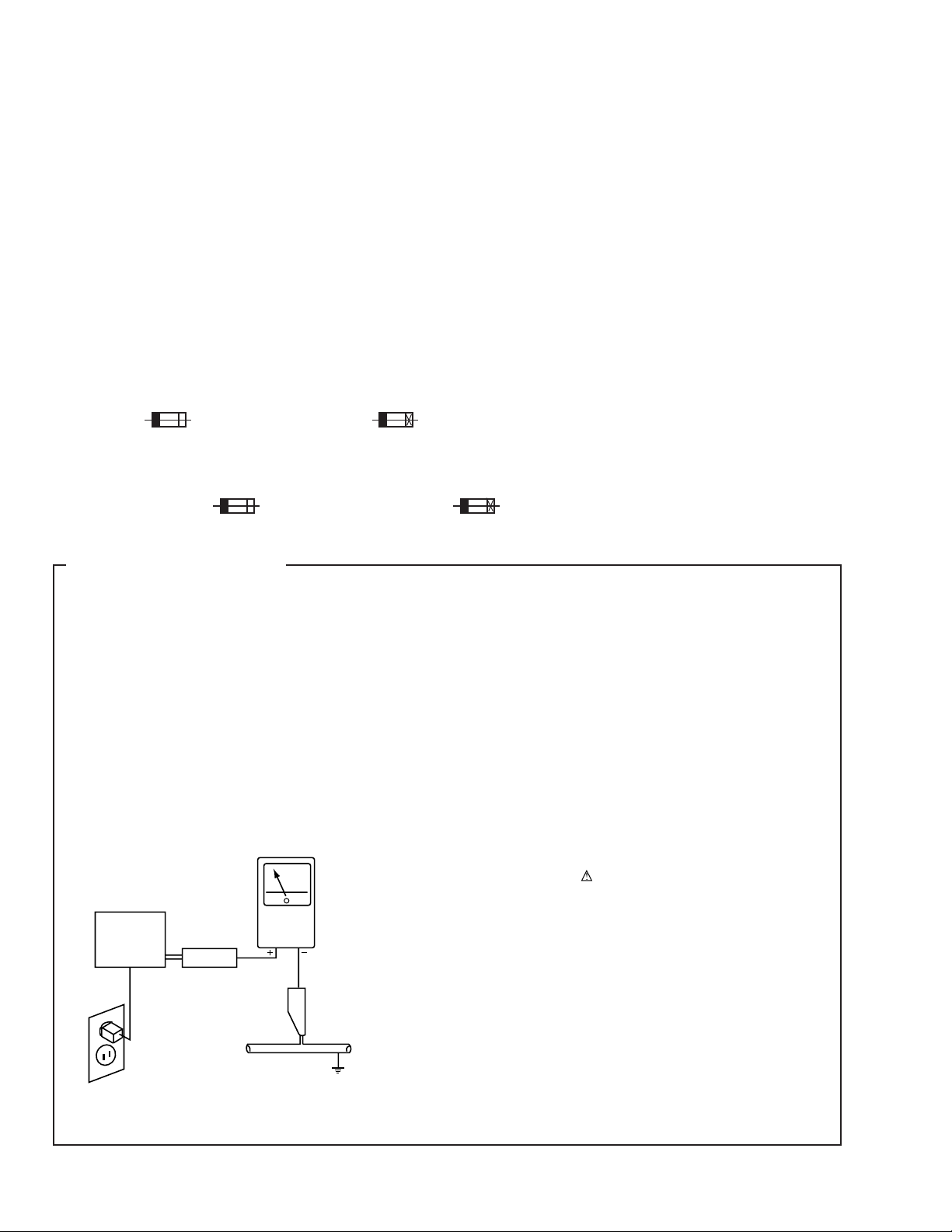
LEAKAGE CURRENT CHECK
Measure leakage current to a known earth ground (water
pipe, conduit, etc.) by connecting a leakage current tester
such as Simpson Model 229-2 or equivalent between the
earth ground and all exposed metal parts of the appliance
(input/output terminals, screwheads, metal overlays, control
shaft, etc.). Plug the AC line cord of the appliance directly
into a 120V AC 60Hz outlet and turn the AC power switch
on. Any current measured must not exceed 0.5mA.
Reading should
not be above
0.5mA
Earth
ground
Device
under
test
Also test with
plug reversed
(Using AC adapter
plug as required)
Leakage
current
tester
Test all
exposed metal
surfaces
ANY MEASUREMENTS NOT WITHIN THE LIMITS
OUTLINED ABOVE ARE INDICATIVE OF A POTENTIAL
SHOCK HAZARD AND MUST BE CORRECTED BEFORE
RETURNING THE APPLIANCE TO THE CUSTOMER.
2. PRODUCT SAFETY NOTICE
Many electrical and mechanical parts in the appliance
have special safety related characteristics. These are
often not evident from visual inspection nor the protection
afforded by them necessarily can be obtained by using
replacement components rated for voltage, wattage, etc.
Replacement parts which have these special safety
characteristics are identified in this Service Manual.
Electrical components having such features are identified
by marking with a
in this Service Manual.
The use of a substitute replacement component which does
not have the same safety characteristics as the PIONEER
recommended replacement one, shown in the parts list in
this Service Manual, may create shock, fire, or other hazards.
Product Safety is continuously under review and new
instructions are issued from time to time. For the latest
information, always consult the current PIONEER Service
Manual. A subscription to, or additional copies of, PIONEER
Service Manual may be obtained at a nominal charge from
PIONEER.
on the schematics and on the parts list
AC Leakage Test
2
Page 3
XR-A670, XR-A370
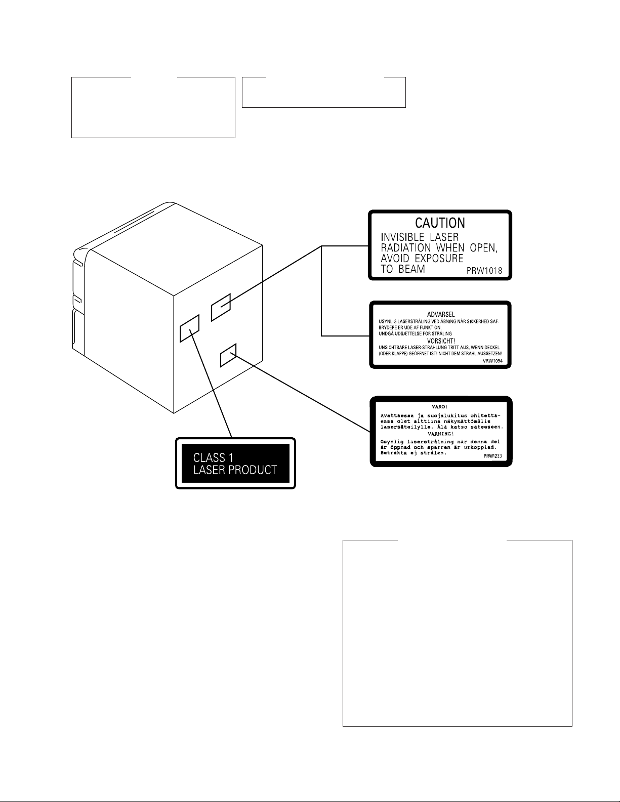
IMPORTANT
THIS PIONEER APPARATUS CONTAINS
LASER OF CLASS 1.
SERVICING OPERATION OF THE APPARATUS
SHOULD BE DONE BY A SPECIALLY
INSTRUCTED PERSON.
LASER DIODE CHARACTERISTICS
MAXIMUM OUTPUT POWER: 5 mW
WAVELENGTH: 780 nm to 785 nm
LABEL CHECK (For MYXJ and NVXJ Types)
NVXJ Type
MYXJ Type
Printed on the Rear Panel
MYXJ Type
Additional Laser Caution
1.Laser Interlock Mechanism
The position of the switch (S9501) for detecting loading
state is detected by the system microprocessor, and
the design prevents laser diode oscillation when the
switch (S9501) is pressed physically.
Thus, the interlock will no longer function if the switch (S9501)
is released physically and deliberatery.
The interlock also does not function in the test mode ∗.
Laser diode oscillation will continue, if pin 1 of
CXA1821M (IC8101) on the CD ASSY mounted on the
$M Loading Mechanism assembly is connected to GND,
or else the terminals of Q8101 are shorted to each other
(fault condition).
2.When the cover is opened, close viewing of the objective
lens with the naked eye will cause exposure to a Class
1 laser beam.
∗
: Refer to page 66.
3
Page 4
XR-A670, XR-A370
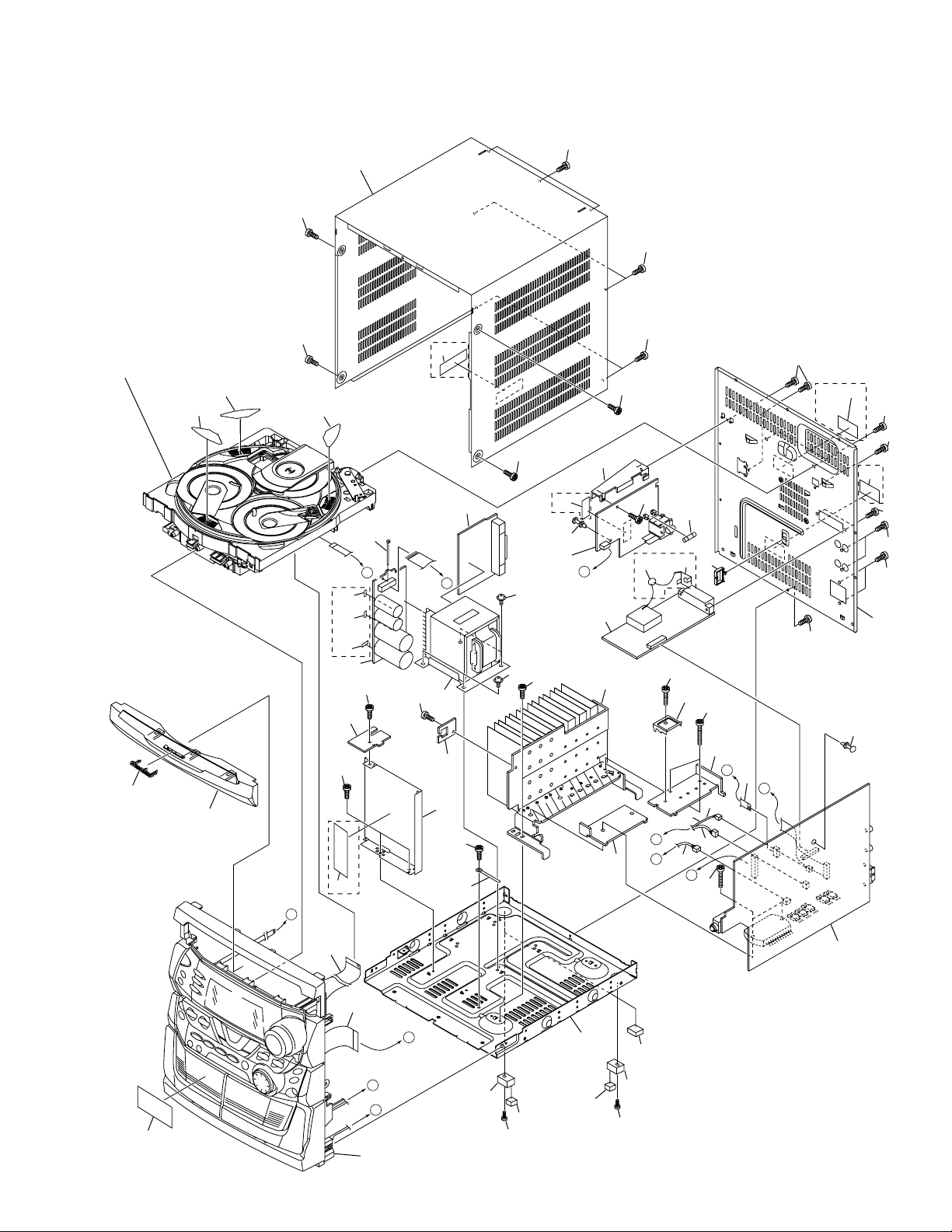
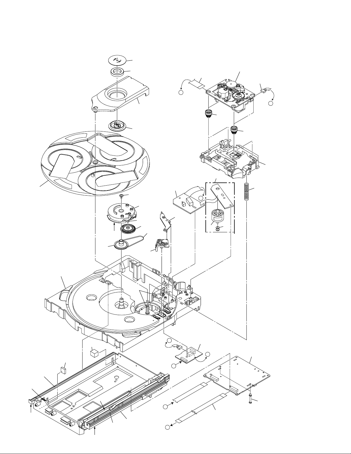
2. EXPLODED VIEWS AND PARTS LIST
NOTES:• Parts marked by "NSP" are generally unavailable because they are not in our Master Spare Parts List.
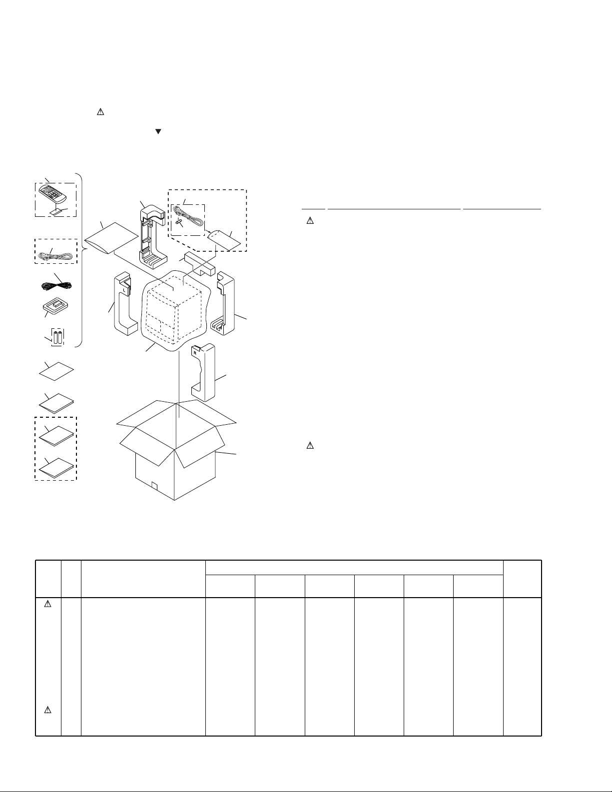
2.1 PACKING
4
S
L
E
E
P
.B
POWER
A
S
S
D
I
S
P
L
A
Y
A
U
X
Except
NVXJ Type
3
6
11
13
14
The mark found on some component parts indicates the importance of the safety factor of the part.
•
Therefore, when replacing, be sure to use parts of identical designation.
Screws adjacent to mark on the product are used for disassembly.
•
V
K
O
A
L
R
A
O
K
E
S
D
F
IS
C
C
P
D
C
IS
L
C
E
A
R
D
P
IS
G
C
M
R
E
P
E
A
T
R
A
N
D
O
M
STATION
R
E
M
O
T
E
C
O
N
T
M
R
O
O
L
N
U
O
N
IT
C
U
B
-X
A
N
R
0
D
2
5
9(1/2)
1
5
12
17
18
1
2
16
8(1/2)
NVXJ Type
Only
9(2/2)
7
8(2/2)
(1) PACKING PARTS LIST
Mark No. Description Part No.
1 Power Cord See Contrast table (2)
2 FM Antenna See Contrast table (2)
3 AM Loop Antenna XTB3001
4 Remote Control Unit XZN3067
(CU-XR060)
5 Battery Cover XZN3065
NSP 6 Dry Cell Battery (R6P, AA) VEM-013
7 Packing Sheet AHG7049
8 Front Pad XHA3013
9 Rear Pad XHA3014
10 Packing Case See Contrast table (2)
NSP 11 Warranty Card See Contrast table (2)
12 Polyethylene Bag Z21-038
(0.03 × 230 × 340)
13 Operating Instructions See Contrast table (2)
(English/French)
14 Operating Instructions See Contrast table (2)
(Italian/Dutch/German)
15 Operating Instructions See Contrast table (2)
(Portuguese/Swedish/Spanish)
16 Sub Pad XHA3017
15
10
NSP 18 Polyethylene Bag See Contrast table (2)
XR-A670/MYXJ and
XR-A370/MYXJ Only
(2) CONTRAST TABLE
XR-A670/MYXJ, NVXJ, KUCXJ, XR-A370/MYXJ, NVXJ and KUCXJ are constructed the same except for the following :
Part No.
17 Fuse (T5A) See Contrast table (2)
Mark No. Symbol and Description
1
Power Cord
2
FM Antenna
10
NSP
NSP
Packing Case
11
Warranty Card
13
Operating Instructions
(English/French)
14
Operating Instructions
(Italian/Dutch/German)
15
Operating Instructions
(Portuguese/Swedish/Spanish)
17
Fuse (T5A)
18
Polyethylene Bag
XR-A670
/MYXJ
ADG1154
ADH7005
XHD3090
ARY7022
XRE3023
XRC3014
XRC3015
Not used
Not used
XR-A670
/NVXJ
ADG1156
ADH7005
XHD3090
ARY7022
XRE3023
Not used
Not used
AEK7001
AHG7033
XR-A670
/KUCXJ
ADG7022
ADH7004
XHD3091
ARY7033
XRE3024
Not used
Not used
Not used
Not used
XR-A370
/MYXJ
ADG1154
ADH7005
XHD3081
ARY7022
XRE3023
XRC3014
XRC3015
Not used
Not used
XR-A370
/NVXJ
ADG1156
ADH7005
XHD3081
ARY7022
XRE3023
Not used
Not used
AEK7001
AHG7033
XR-A370
/KUCXJ
ADG7022
ADH7004
XHD3082
ARY7033
XRE3024
Not used
Not used
Not used
Not used
Remarks
4
Page 5
B
C
D
A
A
B
C
D
E
E
F
F
Refer to
"2.3 FRONT PANEL SECTION".
Refer to
"2.4 $M MECHANISM CD-2".
6
30
30
30
21
2
7
4
51
50
50
51
51
54
54
8
25
53
28
26
31
20
46
14
18
17
16
15
3
11
35
5
1
48
48
48
49
55
55
37
38 or 44
55
55
55
55
49
49
48
49
41
40
42
45
KUCXJ
Type
Only
Except
NVXJ
Type
XR-A670
Only
KUCXJ Type
Only
Except
KUCXJ
Type
Except
KUCXJ Type
MYXJ
Type
Only
24
29
52
52
47
27
9
32
12
43
13
33
34
36
22
23
19
39
56
50
56
50
57
57
Note :
Attatch on the same numbers × three.
Note :
Hook Tray cap on top of loading
tray and then insert the bottom
three hooks.
10
52
2.2 EXTERIOR SECTION
XR-A670, XR-A370
5
Page 6

XR-A670, XR-A370
(1) EXTERIOR SECTION PARTS LIST
Mark No. Description Part No. Mark No. Description Part No.
1 AF Assy See Contrast table (2)
2 PRIMARY Assy See Contrast table (2)
3 SUB TRANS Assy See Contrast table (2)
4 SECONDARY Assy See Contrast table (2)
5 FM/AM TUNER Module See Contrast table (2)
NSP 6 $M Mechanism CD-2 See Contrast table (2)
7 Power Transformer See Contrast table (2)
8 Fuse (FU1) See Contrast table (2)
NSP 9 Fuse Caution Label See Contrast table (2)
10 Card Spacer XEC3008
11 Card Spacer XEC3011
12 25P 120 Flexible Cable/60V XDD3034
(AF CN5101 ↔ DISPLAY CN5503)
13 19P 190 Flexible Cable/30V XDD3038
(CD CN8201 ↔ DISPLAY CN5501)
14 08P 230 Flexible Cable/30V XDD3039
(AF CN1052 ↔ CD CN8204)
15 Connector Assy 5P See Contrast table (2)
(AF CN2301, CN2302 ↔ DECK)
16 Connector Assy 3P XDE3021
(AF CN2303 ↔ DECK)
17 Connector Assy 3P See Contrast table (2)
(AF CN2301 ↔ DECK)
18 Connector Assy 2P See Contrast table (2)
(AF CN2302 ↔ DECK)
NSP 19 Chassis XNA3004
20 Rear Panel See Contrast table (2)
21 Bonnet Case See Contrast table (2)
22 Tray Cap See Contrast table (2)
23 Pioneer Badge XAM3001
24 Heat Sink See Contrast table (2)
25 PCB Bracket XMR3007
26 Earth Plate See Contrast table (2)
27 Shield Plate XNG3017
28 Wire Clip A XEC3003
29 Sub Heat Sink B XNH3012
30 Disc Label XAX3127
31 Ceramic Capacitor See Contrast table (2)
32 Cord Clamper RNH-184
NSP 33 Support Assy XWZ3205
NSP 34 Cable Holder XWZ3206
NSP 35 Fuse Card See Contrast table (2)
36 Binder ZCA-SKB90BK
37 Caution Label HE See Contrast table (2)
38 Caution Label See Contrast table (2)
39 Cushion Leg B XEB3009
40 ICP Label See Contrast table (2)
41 ICP Label See Contrast table (2)
42 ICP Label See Contrast table (2)
NSP 43 Getter See Contrast table (2)
44 Caution Label See Contrast table (2)
45 65 Label See Contrast table (2)
NSP 46 Sub Heat Sink A XNH3011
NSP 47 FET Bracket XNG3016
48 Screw BPZ30P080FZK
49 Screw VBT30P080FZK
50 Screw BBZ30P060FMC
51 Screw BBZ30P080FMC
52 Screw BBZ30P180FMC
53 Screw BPZ30P080FMC
54 Screw ASZ40P060FMC
55 Screw BPZ30P100FZK
56 Cushion Leg A XEB3008
57 Leg XMR3012
6
Page 7
XR-A670, XR-A370
(2) CONTRAST TABLE
XR-A670/MYXJ, NVXJ, KUCXJ, XR-A370/MYXJ, NVXJ and KUCXJ are constructed the same except for the following :
Part No.
Mark No. Symbol and Description
1
AF Assy
2
PRIMARY Assy
3
SUB TRANS Assy
4
SECONDARY Assy
5
FM/AM TUNER Module
XR-A670
/MYXJ
XWZ3200
XWZ3213
XWZ3208
XWZ3221
AXQ7068
XR-A670
/NVXJ
XWZ3200
XWZ3213
XWZ3208
XWZ3221
AXQ7068
XR-A670
/KUCXJ
XWZ3199
XWZ3224
XWZ3227
XWZ3221
AXQ7065
XR-A370
/MYXJ
XWZ3197
XWZ3225
XWZ3228
XWZ3220
AXQ7068
XR-A370
/NVXJ
XWZ3197
XWZ3225
XWZ3228
XWZ3220
AXQ7068
XR-A370
/KUCXJ
XWZ3196
XWZ3224
XWZ3227
XWZ3220
AXQ7065
Remarks
NSP
NSP
NSP
NSP
6
$M Mechanism CD-2
7
Power Transformer
8
Fuse (FU1 : T5A)
8
Fuse (FU1 : 5A)
8
Fuse (FU1 : 6.3A)
8
Fuse (FU1 : T4A)
9
Fuse Caution Label
15
Connector Assy 5P
17
Connector Assy 3P
18
Connector Assy 2P
20
Rear Panel
21
Bonnet Case
22
Tray Cap
24
Heat Sink
26
Earth Plate
31
Ceramic Capacitor
35
Fuse Card
37
Caution Label HE
38
Caution Label
40
ICP Label
41
ICP Label
42
ICP Label
43
Getter
44
Caution Label
45
65 Label
XXA3012
XTS3031
AEK1061
Not used
Not used
Not used
Not used
XDE3020
Not used
Not used
XNC3039
XZN3098
XAK3091
XNH3010
XNG3015
CKPUYB102K50
AAX7098
PRW1233
VRW1094
XAX3121
XAX3153
XAX3158
XAX3142
Not used
Not used
XXA3012
XTS3031
AEK1061
Not used
Not used
Not used
Not used
XDE3020
Not used
Not used
XNC3039
XZN3098
XAK3091
XNH3010
XNG3015
CKPUYB102K50
Not used
Not used
Not used
XAX3121
XAX3153
XAX3158
XAX3142
PRW1018
Not used
XXA3012
XTS3032
Not used
Not used
REK1085
Not used
XAX3157
XDE3020
Not used
Not used
XNC3040
XZN3098
XAK3091
XNH3010
Not used
Not used
AAX2374
Not used
Not used
XAX3121
XAX3153
XAX3158
XAX3143
Not used
ORW1069
XXA3009
XTS3016
Not used
Not used
Not used
AEK1060
Not used
XDE3020
Not used
Not used
XNC3034
XZN3097
XAK3085
XNH3009
XNG3015
CKPUYB102K50
Not used
PRW1233
VRW1094
Not used
Not used
Not used
XAX3137
Not used
Not used
XXA3009
XTS3016
Not used
Not used
Not used
AEK1060
Not used
XDE3020
Not used
Not used
XNC3034
XZN3097
XAK3085
XNH3009
XNG3015
CKPUYB102K50
Not used
Not used
Not used
Not used
Not used
Not used
XAX3137
PRW1018
Not used
XXA3009
XTS3017
Not used
REK1083
Not used
Not used
XAX3122
Not used
XDE3022
XDE3023
XNC3035
XZN3098
XAK3091
XNH3009
Not used
Not used
AAX7097
Not used
Not used
Not used
Not used
Not used
XAX3138
Not used
ORW1069
7
Page 8
XR-A670, XR-A370
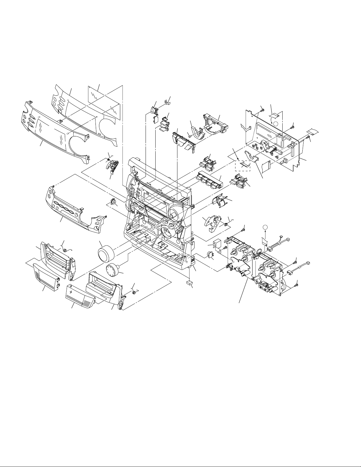
2.3 FRONT PANEL SECTION
32
17
30
11
15
31
24
25
18
13
38
4
9
6
10
14
XR-A670
Only
22
20
23
27
5
38
3
6
26
35 or 36
38
16 or 34
A
38
A
38
1
38
19
7
28
29
33
12
21
8
37
2
Refer to
"2.6 MECHANISM UNIT".
38
8
Page 9
XR-A670, XR-A370
(1) FRONT PANEL SECTION PARTS LIST
Mark No. Description Part No. Mark No. Description Part No.
1 DISPLAY Assy See Contrast table (2)
2 Mechanism Unit See Contrast table (2)
3 Earth Plate B XNG3023
4 Ratch Spring_L ABH7130
5 Ratch Spring_R ABH7131
6 Damper Assy AXA7052
7 Door Spring_L XBH3001
8 Door Spring_R XBH3002
9 Ratch Mold_L XMR3001
10 Ratch Mold_R XMR3002
11 Volume Knob See Contrast table (2)
12 JOG Knob See Contrast table (2)
13 V Button A See Contrast table (2)
14 V Button B See Contrast table (2)
15 FL Filter XAK3089
16 LT Conductor See Contrast table (2)
17 Display Panel See Contrast table (2)
18 V Lens XAK3117
19 FL Cover See Contrast table (2)
20 LED Cover See Contrast table (2)
21 Front Panel See Contrast table (2)
22 Function Button A XZN3087
23 S.C. Button XZN3080
24 POWER Button See Contrast table (2)
25 CD Button XZN3079
26 Function Button B XZN3102
27 JOG Lens XZN3082
28 Deck Lens L XZN3077
29 Deck Lens R XZN3078
30 Sub Panel XZN3093
31 ST Lens XZN3101
32 Deck Door_L See Contrast table (2)
33 Deck Door_R See Contrast table (2)
34 V Cap See Contrast table (2)
35 17P 180 Flexible Cable/60V See Contrast table (2)
(DISPLAY CN2903 ↔ DECK CN2905)
36 15P 180 Flexible Cable/60V See Contrast table (2)
(DISPLAY CN2903 ↔ DECK CN2905)
37 Cushion Leg A XEB3008
38 Screw BPZ30P080FMC
(2) CONTRAST TABLE
XR-A670/MYXJ, NVXJ, KUCXJ, XR-A370/MYXJ, NVXJ and KUCXJ are constructed the same except for the following :
Part No.
Mark No. Symbol and Description
1
DISPLAY Assy
2
Mechanism Unit
11
Volume Knob
12
JOG Knob
13
V Button A
XR-A670
/MYXJ
XWZ3215
XYM3010
XAA3013
XAA3014
XAD3034
XR-A670
/NVXJ
XWZ3215
XYM3010
XAA3013
XAA3014
XAD3034
XR-A670
/KUCXJ
XWZ3214
XYM3010
XAA3013
XAA3014
XAD3034
XR-A370
/MYXJ
XWZ3210
XYM3010
XAA3011
XAA3012
XAD3025
XR-A370
/NVXJ
XWZ3210
XYM3010
XAA3011
XAA3012
XAD3025
XR-A370
/KUCXJ
XWZ3209
XYM3008
XAA3013
XAA3014
XAD3034
Remarks
14
V Button B
16
LT Conductor
17
Display Panel
19
FL Cover
20
LED Cover
21
Front Panel
24
POWER Button
30
Sub Panel
32
Deck Door_L
33
Deck Door_R
34
V Cap
35
17P 180 Flexible Cable/60V
36
15P 180 Flexible Cable/60V
XAD3039
XAK3090
XAK3112
XAK3124
XMR3009
XMB3023
XAD3027
XAK3105
XAN3015
XAN3016
Not used
XDD3032
Not used
XAD3039
XAK3090
XAK3112
XAK3124
XMR3009
XMB3023
XAD3027
XAK3105
XAN3015
XAN3016
Not used
XDD3032
Not used
XAD3039
XAK3090
XAK3113
XAK3088
XMR3009
XMB3023
XAD3033
XAK3106
XAN3015
XAN3016
Not used
XDD3032
Not used
XAD3038
Not used
XAK3078
XAK3124
Not used
XMB3022
XAD3022
XAK3079
XAN3013
XAN3014
XAK3083
XDD3032
Not used
XAD3038
Not used
XAK3078
XAK3124
Not used
XMB3022
XAD3022
XAK3079
XAN3013
XAN3014
XAK3083
XDD3032
Not used
XAD3039
Not used
XAK3108
XAK3088
Not used
XMB3023
XAD3027
XAK3080
XAN3019
XAN3016
XAK3083
Not used
XDD3033
9
Page 10
XR-A670, XR-A370
2.4 $M MECHANISM CD-2
12
29
26
8
7
A
14
13
2
15
19
29
18
6
21
C
27
Refer to
"2.5 SERVO MECHANISM ASSY".
25
22
D
24
23
11
1
5
28
29
29
29
10
30
32
29
16
29
17
29
D
B
A
9
B
4
C
31
3
20
10
29
Page 11
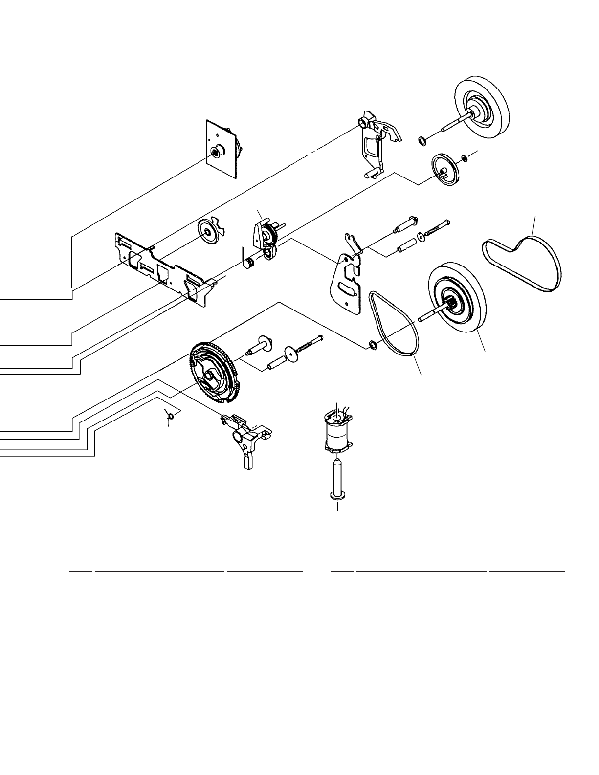
(1) $M MECHANISM CD-2 PARTS LIST
(2) CONTRAST TABLE
$M Mechanism CD-2 (XXA3012) and (XXA3009) are constructed the same except for the following :
Mark No. Symbol and Description
Part No.
Remarks
XXA3012 (XR-A670) XXA3009 (XR-A370)
3 CD Assy XWZ3233 XWZ3229
XR-A670, XR-A370
Mark No. Description Part No.
1 MOTOR Assy XWZ3230
2 SW Assy XWZ3231
3 CD Assy See Contrast table (2)
4 TRADE Assy XWZ3232
5 Servo Spring ABH7126
6 Belt AEB7072
7 Clamp Magnet AMF7001
8 Yoke ANB7216
9 Mecha Base XNW3011
10 Loading Tray XNW3002
11 Traverse Base XNW3006
12 Rotary Tray ANW7124
13 Clamper XNW3007
14 Clamper Holder XNW3004
15 Main Cam ANW7093
Mark No. Description Part No.
16 Gear Pulley ANW7094
17 Lock Lever ANW7095
18 Planet Gear ANW7096
19 Actuator ANW7097
20 Mini Card Spacer AEC7143
21 16P 200 Flexible Cable/60V XDD3036
22 Connector Assy (6P) ADE7010
23 Float Rubber A AEB7063
24 Float Rubber B AEB7066
25 Servo Mechanism Assy XXA3010
26 Screw IPZ30P080FMC
27 Carriage Motor VXM1033
28 Motor Pulley PNW1634
29 Ha Narl GEM1016
30 Cushion Rubber XEB3005
31 11P 185 Flexible Cable/30V XDD3037
32 Cushion Rubber XEB3007
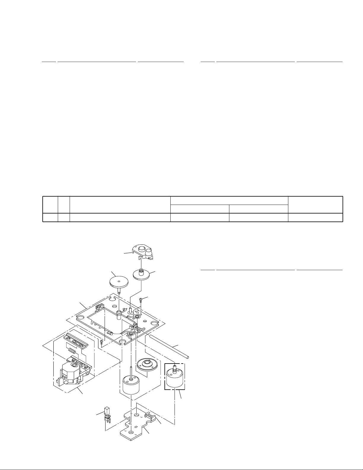
2.5 SERVO MECHANISM ASSY
No supplied part
4
1
14
9
5
SERVO MECHANISM ASSY PARTS LIST
•
Mark No. Description Part No.
NSP 1 Motor Chassis Assy • • • • •
NSP 5 Screw +P2*3 • • • • •
3
2
2 Motor Gear Assy X-2625-769-(1)
3 Sled Shaft 2-626-908-(01)
4 Gear (A)(S) 2-625-188-(02)
6 Leaf Switch 1-572-085-(11)
7 Motor(6p)(S)PCB 1-639-678-(12)
8 Connector Pin 6p 1-564-722-(11)
9 Gear(B)(RP) 2-627-003-(01)
10 • • • • •
11 • • • • •
12 • • • • •
13 • • • • •
14 KSS-213C(Pick-up) 8-848-483-(05)
6
8
7
11
Page 12
XR-A670, XR-A370
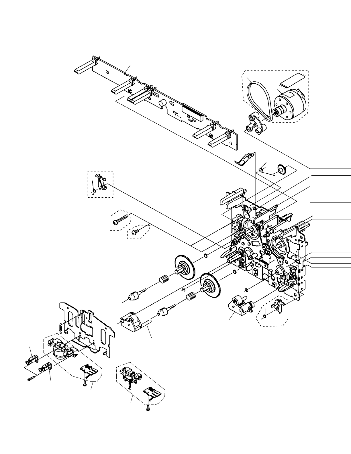
2.6 MECHANISM UNIT
Mech. Ι
Only
Mech. Ι
Mech. ΙΙ
4
Only
Mech. ΙΙ
Only
7
2
12
Mech. ΙΙ
13
Mech. ΙΙ
9
Mech. ΙΙ
Only
10
1
2
Mech. Ι
12
Page 13
XR-A670, XR-A370
5
8
11
6
MECHANISM UNIT PARTS LIST
•
(XYM3010)
Mark No. Description Part No.
1 Plate HD BLK (Mech. ΙΙ) F513-847
2 Plate HD BLK (Mech. Ι) F513-846
3 Motor Main BLK (Mech. ΙΙ only) F525-329
4 PCB Control BLK F567-630
5 Clutch Assy BLK F522-049
6 Main Belt FF19N-11
7 Joint Belt 113 (Mech. ΙΙ only) FF19P-11
8 Clutch Assy BLK (Mech. Ι) FR25B-11
8 Clutch Assy BLK (Mech. ΙΙ) FR24Y-11
9 Roller Pinch BLK R F514-129
10 Roller Pinch BLK L F514-130
11 F/R Belt FF19S-11
12 Plate Base BLK F512-127
13 Plate Base BLK F512-128
MECHANISM UNIT PARTS LIST
•
(XYM3008 : XR-A370/KUCXJ)
Mark No. Description Part No.
1 Plate HD BLK (Mech. ΙΙ) F513-848
2 Plate HD BLK (Mech. Ι) F513-846
3 Motor Main BLK (Mech. ΙΙ only) F525-329
4 PCB Control BLK F567-631
5 Clutch Assy BLK F522-049
6 Main Belt FF19N-11
7 Joint Belt 113 (Mech. ΙΙ only) F19N-11
8 Clutch Assy BLK (Mech. Ι) FR25B-11
8 Clutch Assy BLK (Mech. ΙΙ) FR24Y-11
9 Roller Pinch BLK R (Mech. ΙΙ) F514-131
10 Roller Pinch BLK L (Mech. ΙΙ) F514-130
11 F/R Belt FF19S-11
12 Plate Base BLK F512-127
13 Plate Base BLK F512-128
13
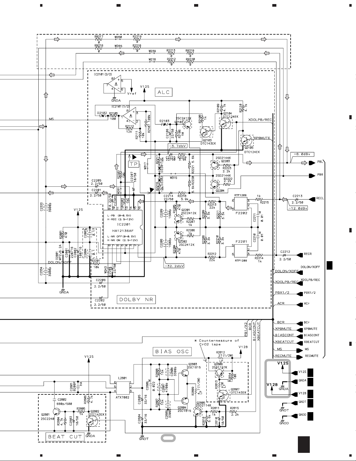
Page 14

1
23
XR-A670, XR-A370
3. BLOCK DIAGRAM AND SCHEMATIC DIAGRAM
3.1 BLOCK DIAGRAM and OVERALL WIRING DIAGRAM
4
V5621
A
J
DISPLAY ASSY
(XR-A670/MYXJ, NVXJ : XWZ3215)
(XR-A670/KUCXJ : XWZ3214)
(XR-A370/MYXJ, NVXJ : XWZ3210)
PDC057A
System Control
(XR-A370/KUCXJ : XWZ3209)
B
IC3001
LC75394NED
17
E-VOL IC
58 55
AA
33
16
21
FL TUBE
29
IC5501
81 82
83
84
IC3101
BA4558F-HT
62 71 1014
AMP
S5951
S5952
STK407-100B (XR-A670)
STK407-070B (XR-A370)
5901
SR
IC3301
Power AMP
67
FM/AM TUNER MODULE
(MYXJ, NVXJ : AXQ7068)
IC3501, IC3502
BA4558F-HT
AB
FM/AM TUNER MODULE
Godzilla Amp
3517
(KUCXJ : AXQ7065)
CN6201
MYXJ, NVXJ
TYPES
C
ONLY
IC5751
BU1923F
RDS IC
4
16
F
AF ASSY
F 1/3- F 3/3
(XR-A670/MYXJ, NVXJ : XWZ3200)
JA3001
(XR-A670/KUCXJ : XWZ3199)
(XR-A370/MYXJ, NVXJ : XWZ3197)
(XR-A370/KUCXJ : XWZ3196)
B
CD ASSY
IC8201
CXD2587Q
DIGITAL
SERVO
D
IC8101
CXA1821M
RF AMP
IC8301
BA5970FP
DRIVER
XR-A670
ONLY
SERVO MECHANISM ASSY
(XXA3010)
TRADE ASSY
E
14
1234
(XWZ3232)
(XR-A670 : XWZ3233)
JA8651
(XR-A370 : XWZ3229)
D
SW ASSY
(XWZ3231)
C
MOTOR ASSY
(XWZ3230)
Page 15
5
678
XR-A670, XR-A370
Note : When ordering service parts, be sure to refer to "EXPLODED VIEWS and P AR TS LIST" or "PCB PARTS LIST".
A
CN3331
JA3441
CN3991
SUPPORT
ASSY
CN11
G
SECONDARY ASSY
(XR-A670 : XWZ3221)
(XR-A370 : XWZ3220)
EXCEPT
XR-A370
/KUCXJ
J81
16
Dolby IC
1
IC2201
HA12136AF
XR-A670
ONLY
IC2301
HA12211NT
89
CABLE
HOLDER
ASSY
T1
POWER TRANSFORMER
(XR-A670/MYXJ, NVXJ : XTS3031)
(XR-A670/KUCXJ : XTS3032)
(XR-A370/MYXJ, NVXJ : XTS3016)
(XR-A370/KUCXJ : XTS3017)
H
PRIMARY ASSY
(XR-A670/MYXJ, NVXJ : XWZ3213)
(XR-A670/KUCXJ, XR-A370/KUCXJ
: XWZ3224)
(XR-A370/MYXJ, NVXJ : XWZ3225)
2627
2 8
REC PB IC
B
C
CN81
SUB TRANS ASSY
I
(XR-A670/MYXJ, NVXJ : XWZ3208)
(XR-A670/KUCXJ, XR-A370/KUCXJ : XWZ3227)
(XR-A370/MYXJ, NVXJ : XWZ3228)
IC81
NJM7805FA
5
RY81
Q81
6
MYXJ, NVXJ
TYPES
ONLY
L1
T2
KUCXJ TYPE
ONLY
FU1
AN1
MYXJ, NVXJ :
50/60Hz AC220-230V
KUCXJ :
60Hz AC120V
D
AC POWER CORD
MYXJ : ADG1154
NVXJ : ADG1156
KUCXJ : ADG7022
15
7
8
Page 16
1
23
XR-A670, XR-A370
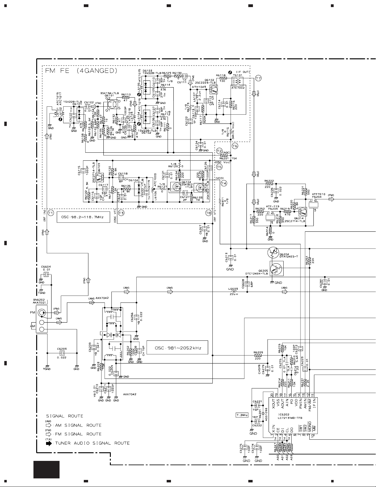
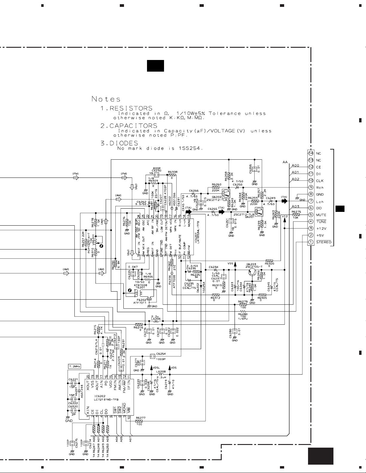
3.2 FM/AM TUNER MODULE (For MYXJ and NVXJ Types)
A
MIX AMP
RF AMP
OSC
B
4
BUFFER
IF AMP
FM +B SW
C
AM RF TUNING BLOCK
D
16
AA
1234
PLL
Page 17
5
678
XR-A670, XR-A370
A
FM/AM TUNER MODULE
AA
(AXQ7068)
B
AF AMP
REGULATOR
CN3051
2/3
F
AF AMP
CN6201
KP200IA14L
C
D
AA
5
6
7
8
17
Page 18
1
23
XR-A670, XR-A370
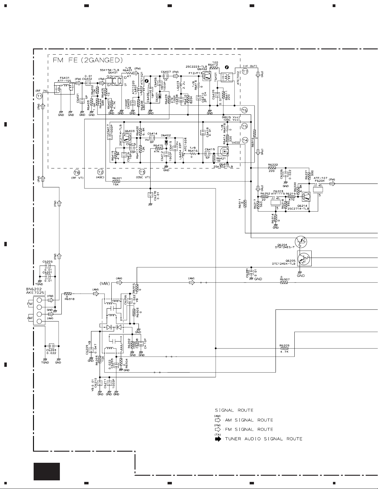
3.3 FM/AM TUNER MODULE (For KUCXJ Type)
4
A
B
RF AMP
1T378A
OSC
1T378A
MIX AMP
BUFFER
IF AMP
FM +B SW
C
MW RF TUNING BLOCK
AKX7041
D
18
AB
1234
Page 19
5
678
XR-A670, XR-A370
FM/AM TUNER MODULE
AB
(AXQ7065)
AF AMP
A
B
CN3051
2/3F
AF AMP
PLL
REGULATOR
CN6201
KP200IA14L
C
D
AB
5
6
7
8
19
Page 20
1
23
XR-A670, XR-A370
3.4 CD, MOTOR, SW and TRADE ASSYS
4
A
CD ASSY (XR-A670 : XWZ3233)
B
(XR-A370 : XWZ3229)
TRADE
E
B
SERVO MECHANISM ASSY
SW ASSY
D
ASSY
(XWZ3232)
CN9001
(S)
S6B-PH-K-S
(S)
(C)
(C)
(S)
(S)
(F)
(F)
(T)
(T)
(S)
(S)
(S)
(S)
(C)
(C)
(S)
(S)(S)
(C)
(C)
(S)
(S)
(C)
(C)
(T)
(T)
(F)
(F)
(F)
(XWZ3231)
J9501
D20PWY0610E
(C)(L)
(L)
(L) (L)
(C)
(L)
(C)
(C)
(L)
(C)
(C)
(F)
CN9002
C
(L)
(L)
J9502
D20PWW0405E
CN9501
52147-0610
SLW11R-1C7
CN8002
SLW11R-1C7
(T)
C
CARRIAGE
S9503
VXM1033
D
SERVO MECHANISM ASSY
CN8101
SLW16R-1C7
20
B C D E
1234
MOTOR
(F)
(T)
(T)
(F)
ASSY
(XWZ3230)
(CD)
(F)
(T)
(F)
(T)
(T)
(F)
MOTOR
(F)
(T)
(CD)(CD)
2
1
Page 21
5
678
XR-A670, XR-A370
: The power supply is shown with the marked box.
(CD)
: CD AUDIO SIGNAL ROUTE
(F)
: FOCUS SERVO LOOP LINE
(T)
: TRACKING SERVO LOOP LINE
(S)
: SPINDLE MOTOR ROUTE
(C)
: CARRIAGE MOTOR ROUTE
(L)
: LOADING MOTOR ROUTE
CN8204
52044-0845
A
CN1052
(CD)
2/3
F
(CD)
(S)
(C)
(C)
(T)
(T)
(F)
(F)
(F)
(T)
(CD)
(CD)(CD)
CN8201
52045-1945
B
CN5501
J
(CD)
(L)
(L)
XR-A670
(T)
(CD)(CD)(CD)
ONLY
(L)
(L)
C
XR-A670
(L)
(L)
ONLY
(CD)
(L)
(L)
Note: The encircled numbers
denote measuring point in the
(L) (L)
(L) (L)
5
6
schematic diagram.
CN8203- Pin 1 :
1
PLAY MODE (RF)
H : 500nsec/div
7
1.8Vp-p
VREF
IC8101- Pin 13 :
2
TEST MODE,
Tracking Open(TRER)
H : 5msec/div
1.0Vp-p
VREF
B
8
D
21
Page 22
1
XR-A670, XR-A370
3.5 AF ASSY (1/3)
23
4
F 1/3
A
B
AF ASSY
(XR-A670/MYXJ, NVXJ : XWZ3200)
(XR-A670/KUCXJ : XWZ3199)
(XR-A370/MYXJ, NVXJ : XWZ3197)
(XR-A370/KUCXJ : XWZ3196)
R2311, R2312 :
22k (XR-A670)
39k (XR-A370)
XR-A670
ONLY
(REC)
XR-A370
ONLY
XR-A670
ONLY
(REC)
(PB)
: DECK PB SIGNAL ROUTE
(REC)
: DECK REC SIGNAL ROUTE
–3.7XR-A670
(PB) (PB)
(PB)
XR-A370
ONLY
XR-A370 ONLY
XR-A370
ONLY
(REC)(REC)
XR-A370
ONLY
XR-A670
ONLY
(REC)(REC)
(REC)
(REC)
(REC)
(REC)
(REC)
D2301-D2306 : 1SS133
(PB) (PB)
(PB) (PB)
CN2301
B3B-PH-K-S
XR-A370
ONLY
CN2302
B2B-PH-K-S
(PB)
33k (XR-A670)
47k (XR-A370)
33k (XR-A670)
47k (XR-A370)
220k (VCP1164): XR-A670
100k (VCP1162): XR-A370
VR2801
220k
XR-A670
ONLY
C
(REC)
MYXJ, NVXJ
TYPES ONLY
(REC)
(PB)
XR-A670 ONLY
XR-A370
ONLY
D
22
F
CN2303
B3B-PH-K-R
1/3
1234
Page 23
5
678
XR-A670, XR-A370
(PB) (PB) (PB)
(PB)
(REC)
XR-A670
(PB)
(PB)
ONLY
(PB) (PB)
BA4558F-HT
(REC)(REC)
BA4558F-HT
(PB)
(PB)
(REC)
1SS355
(REC)
(PB)
XR-A370
ONLY
(REC)(REC)
A
(PB)(PB)
(REC)
(PB)
B
(REC)
XR-A670/
MYXJ, NVXJ
ONLY
XR-A670
ONLY
(REC)
3/3
F
2/3,3/3
F
F
2/3
C
3/3
F
XR-A670
ONLY
XR-A670
ONLY
5
6
: The power supply is shown with the marked box.
7
F
3/3
F
2/3
F
1/3
8
23
D
Page 24
1
XR-A670, XR-A370
3.6 AF ASSY (2/3)
F 2/3
AF ASSY
A
B
(XR-A670/MYXJ, NVXJ : XWZ3200)
(XR-A670/KUCXJ : XWZ3199)
(XR-A370/MYXJ, NVXJ : XWZ3197)
(XR-A370/KUCXJ : XWZ3196)
MYXJ,
NVXJ
TYPES ONLY
23
CN8204
B
CN1052
52045-0845
MYXJ,
NVXJ
TYPES ONLY
0.056 (MYXJ,NVXJ)
0.027 (KUCXJ)
MYXJ,
NVXJ
TYPES
ONLY
0.56 (MYXJ,NVXJ)
0.47 (KUCXJ)
0.1 (MYXJ,NVXJ)
0.068 (KUCXJ)
0.33
4
3/3
F
0.47/50
IC300
LC75394NED
0.47/50
: AUDIO SIGNAL ROUTE
0.33
0.056 (MYXJ,NVXJ)
0.027 (KUCXJ)
C
: CD AUDIO SIGNAL ROUTE
: TUNER AUDIO SIGNAL ROUTE
: DECK PB SIGNAL ROUTE
: DECK REC SIGNAL ROUTE
0.56 (MYXJ,NVXJ)
0.47 (KUCXJ)
0.1 (MYXJ,NVXJ)
0.068 (KUCXJ)
0.47/50 (MYXJ,NVXJ)
2.2/50 (KUCXJ)
2.2/50 (MYXJ,NVXJ)
10/50 (KUCXJ)
0.47/50 (MYXJ,NVXJ)
2.2/50 (KUCXJ)
0.47/50 (MYXJ,NVXJ)
2.2/50 (KUCXJ)
4.7/50 (MYXJ,NVXJ)
10/50 (KUCXJ)
BA4558F-HT
CN5102
D
CN5503
J
24
F
2/3
52045-2545
XR-A670
ONLY
BA4558F-HT
1234
Page 25

5
CN6201 (MYXJ, NVXJ TYPES)
AA
CN6201 (KUCXJ TYPE)
AB
678
XR-A670, XR-A370
CN3051
KM200IB14
MYXJ, NVXJ
TYPES
ONLY
MYXJ, NVXJ
TYPES ONLY
3.9k (MYXJ,NVXJ)
4.7k (KUCXJ)
3.9k (MYXJ,NVXJ)
4.7k (KUCXJ)
MYXJ, NVXJ
TYPES ONLY
MYXJ, NVXJ
TYPES ONLY
BA4558F-HT (1/2)
BA4558F-HT (1/2)
MYXJ, NVXJ TYPES ONLY
F
3/3
F
A
3/3
B
3/3
F
1/3,3/3
F
3/3
3/3
F
3/3
F
2/3
8
F
25
XR-A670
ONLY
3/3
F
1/3
F
5
6
7
F
C
D
Page 26

1
23
XR-A670, XR-A370
3.7 AF (3/3) and SECONDARY ASSYS
A
R3515,R3516,R3517,R3518
1.5k (MYXJ, NVXJ)
1.2k (KUCXJ)
2/3
F
B
IRF9540G (XR-A670)
IRFI9Z34G (XR-A370)
2/3
F
IRF540G
(XR-A670)
IRFIZ34G
(XR-A370)
1SR139-100
D3302
1SR139-100
MYXJ, NVXJ
TYPES
ONLY
56k
56k
BA4558F-HT (1/2)
4
STK407-100B (XR-A670)
STK407-070B (XR-A370)
1k (MYXJ, NVXJ)
0 (KUCXJ)
MYXJ, NVXJ
TYPES
ONLY
56k (MYXJ, NVXJ)
68k (KUCXJ)
BA4558F-HT (1/2)
47k (XR-A670)
39k (XR-A370/MYXJ, NVXJ)
47k (XR-A370/KUXJ)
BA4558F-HT (2/2)
2/3
F
1/3, 2/3
F
2/3
F
2/3
C
F
F
F
2/3
2/3
XR-A370/KUCXJ
ONLY
EXCEPT
XR-A370/KUCXJ
BA4558F-HT (2/2)
1/3
F
2/3
F
D
2/3
F
: The power supply is shown with the marked box.
26
3/3
F
1234
Page 27

5
678
XR-A670, XR-A370
F 3/3
CAUTION : FOR CONTINUED PROTECTION AGAINST
CAUTION : FOR CONTINUED PROTECTION AGAINST
AF ASSY
RISK OF FIRE. REPLACE ONLY WITH SAME
TYPE NO. 4911.25 MFD, BY LITTELFUSE INK.
FOR IC71 (AEK7010).
RISK OF FIRE. REPLACE ONLY WITH SAME
TYPE NO. 491003 MFD, BY LITTELFUSE INK.
FOR IC41 (AEK7050).
(XR-A670/MYXJ, NVXJ : XWZ3200)
(XR-A670/KUCXJ : XWZ3199)
(XR-A370/MYXJ, NVXJ : XWZ3197)
(XR-A370/KUCXJ : XWZ3196)
: AUDIO SIGNAL ROUTE
100 (MYXJ, NVXJ)
10 (KUCXJ)
820
100 (MYXJ, NVXJ)
10 (KUCXJ)
KUCXJ TYPE
ONLY
CAUTION : FOR CONTINUED PROTECTION AGAINST
CAUTION : FOR CONTINUED PROTECTION AGAINST
MYXJ, NVXJ
TYPES ONLY
RISK OF FIRE. REPLACE ONLY WITH SAME
TYPE NO. 491004 MFD, BY LITTELFUSE INK.
FOR IC31 (AEK7053: XR-A670).
RISK OF FIRE. REPLACE ONLY WITH SAME
TYPE NO. 491003 MFD, BY LITTELFUSE INK.
FOR IC31 (AEK7050: XR-A370).
CN3331
AKE7001
MYXJ, NVXJ
TYPES ONLY
JA3441
VKB1060
XR-A670
ONLY
A
B
8.2k (XR-A670)
5.6k (XR-A370)
MYXJ, NVXJ
TYPES ONLY
CN11
KPE15
4700/80 (XCH3001 : XR-A670)
3300/63 (AXH7071 : XR-A370)
S1WB(A)60SBD (XR-A670)
S1WB(A)60SD (XR-A370)
S1WB(A)60SBD (XR-A670)
S1WB(A)60SD (XR-A370)
J11
D15A15-350-2651
SECONDARY ASSY (XR-A670 : XWZ3221)
G
CAUTION : FOR CONTINUED PROTECTION AGAINST
CAUTION : FOR CONTINUED PROTECTION AGAINST
RISK OF FIRE. REPLACE ONLY WITH SAME
TYPE NO. 491010F MFD, BY LITTELFUSE INK.
FOR IC11 AND IC12 (AEK7068: XR-A670).
RISK OF FIRE. REPLACE ONLY WITH SAME
TYPE NO. 491007 MFD, BY LITTELFUSE INK.
FOR IC11 AND IC12 (AEK7047: XR-A370).
PHONES
CN3991
AKN-056
1.25A
AEK7021 (7A) : XR-A670
AEK7019 (5A) : XR-A370
AEK7021 (7A) : XR-A670
AEK7019 (5A) : XR-A370
AEK7053 (4A) : XR-A670
AEK7050 (3A) : XR-A370
AEK7068 (10A) : XR-A670
AEK7047 (7A) : XR-A370
T1
POWER TRANSFORMER
(XR-A370 : XWZ3220)
CAUTION : FOR CONTINUED PROTECTION AGAINST
CAUTION : FOR CONTINUED PROTECTION AGAINST
RISK OF FIRE. REPLACE ONLY WITH SAME
TYPE NO. 491007 MFD, BY LITTELFUSE INK.
FOR IC21 AND IC22 (AEK7021: XR-A670).
RISK OF FIRE. REPLACE ONLY WITH SAME
TYPE NO. 491005 MFD, BY LITTELFUSE INK.
FOR IC21 AND IC22 (AEK7019: XR-A370).
C
D
3/3
F
5
6
7
G
8
27
Page 28

1
23
XR-A670, XR-A370
3.8 PRIMARY and SUB TRANS ASSYS
A
4
XR-A670/
MYXJ, NVXJ
ONLY
120
B
10
230
120
XR-A670/
MYXJ, NVXJ
ONLY
(XR-A370/
MYXJ, NVXJ)
(KUCXJ)
XR-A670/
MYXJ, NVXJ
ONLY
EXCEPT
XR-A670/
MYXJ, NVXJ
XR-A670/
MYXJ, NVXJ
ONLY
EXCEPT
XR-A670/
MYXJ, NVXJ
EXCEPT
XR-A670/
MYXJ, NVXJ
T1 POWER TRANSFORMER
C
J81
J
CN81
52147-0410
NJM7805FA
S1WB(A)60-4062
D
28
H I
1234
Page 29

5
678
XR-A670, XR-A370
A
PRIMARY ASSY
H
(XR-A670/MYXJ, NVXJ : XWZ3213)
(XR-A670/KUCXJ, XR-A370/KUCXJ : XWZ3224)
(XR-A370/MYXJ, NVXJ : XWZ3225)
B
MYXJ, NVXJ TYPES
KUXJ TYPE
• NOTE FOR FUSE REPLACEMENT
CAUTION -
MYXJ, NVXJ
TYPES ONLY
L1
ATF1136 (XR-A670)
XTF3001 (XR-A370)
FOR CONTINUED PROTECTION AGAINST RISK OF FIRE.
REPLACE WITH SAME TYPE AND RATINGS ONLY.
FU1
XR-A670/MYXJ, NVXJ :
AEK1061 (T5A)
XR-A670/KUCXJ :
REK1085 (6.3A)
XR-A370/MYXJ, NVXJ :
AEK1060 (T4A)
XR-A370/KUCXJ :
REK1083 (5A)
I
SUB TRANS ASSY
(XR-A670/MYXJ, NVXJ : XWZ3208)
(XR-A670/KUCXJ, XR-A370/KUCXJ
: XWZ3227)
(XR-A370/MYXJ, NVXJ : XWZ3228)
AN1
AN1
XKP3041 (MYXJ, NVXJ)
XKP3042 (KUCXJ)
KUCXJ
TYPE
ONLY
C
D
H I
5
6
7
8
29
Page 30

1
XR-A670, XR-A370
3.9 DISPLAY ASSY
A
B
23
DISPLAY ASSY
J
(XR-A670/MYXJ, NVXJ : XWZ3215)
(XR-A670/KUCXJ : XWZ3214)
(XR-A370/MYXJ, NVXJ : XWZ3210)
(XR-A370/KUCXJ : XWZ3209)
4
6Mz
C
MYXJ, NVXJ
XR-A670
ONLY
XR-A670
ONLY
XR-A670
ONLY
D
300 (XR-A670)
390 (XR-A370)
TYPES ONLY
XR-A670
ONLY
KUCXJ
TYPE ONLY
SYSTEM CONTROL
30
J
1234
Page 31

5
678
XR-A670, XR-A370
J81
D20PYY0425E
I
CN81
CN8201
B
KUCXJ TYPE
ONLY
CN5501
52492-1920
CN5503
52045-2545
XR-A670
ONLY
F
2/3
CN5102
52045-1745 (OTHERS)
52045-1545 (XR-A370/KUCXJ)
DECK MECHA
CN2903
EXCEPT
XR-A370
/KUCXJ
A
B
1SS181
1SS181
KUCXJ TYPE
ONLY
S5911-S5917, S5919-S5936 : XSG3001
MYXJ, NVXJ
TYPES ONLY
XR-A670 ONLY
C
S5911 : DISC 1
S5912 : DISC 2
S5913 : DISC 3
S5914 : STANDBY/ON (POWER)
S5915 : DISC CHANGE
S5916 : OPEN/CLOSE
S5917 : 2 NR ON/OFF
5
6
S5919 : CD
S5920 : AUX •
S5921 : TUNING + ¡ • ¢
S5922 : STOP/ST.MEMORY 7
S5923 : PLAY/PAUSE 2 3
S5924 : TUNING – 4 • 1
S5925 : TUNER/BAND
S5926 : TAPEΙ/ΙΙ
S5927 : FREQ/STATION
S5928 : REC/STOP
S5929 : PRESET
S5930 : ASES/COPY
S5931 : EQUALIZER
S5932 : ZOOM SURROUND
7
S5933 : P.BASS (DEMO)
S5934 : SET
S5935 : DISPLAY
S5936 : TIMER/CLOCK ADJ
S5951 : VOLUME
S5952 : SOUND MORPHING JOG
J
8
D
31
Page 32

1
23
XR-A670, XR-A370
4. PCB CONNECTION DIAGRAM
NOTE FOR PCB DIAGRAMS :
A
1. Part numbers in PCB diagrams match those in the schematic
diagrams.
2. A comparison between the main parts of PCB and schematic
diagrams is shown below.
Symbol In PCB
Diagrams
BCE
BCE
D
Symbol In Schematic
Diagrams
BCEBCE
BCE
BCE
DGS
DGGSS
Part Name
Transistor
Transistor
with resistor
Field effect
transistor
Resistor array
3-terminal
regulator
4.1 FM/AM TUNER MODULE (For MYXJ and NVXJ Types)
B
FM/AM TUNER MODULE
AA
3. The parts mounted on this PCB include all necessary parts for
several destinations.
For further information for respective destinations, be sure to
check with the schematic diagram.
4. View point of PCB diagrams.
Connector
Capacitor
SIDE A
P.C.Board
Chip Part
SIDE B
CN3051
F
4
SIDE A
C
Q6204 Q6203
FM/AM TUNER MODULE
AA
VR6201
SIDE B
D
32
AA
Q6101
Q6501
Q6102 - Q6105 Q6205
Q6214
Q6601
Q6202
IC6202
Q6201
IC6201
(ANP7160-B)
1234
Page 33

1
234
4.2 FM/AM TUNER MODULE (For KUCXJ Type)
FM/AM TUNER MODULE
AB
CN3051
F
XR-A670, XR-A370
A
B
FM/AM TUNER MODULE
AB
Q6204
SIDE A
VR6201
Q6203
C
(ANP7159-B)
Q6306
Q6304
Q6401
Q6402
Q6303Q6302 Q6301
Q6214
Q6403
Q6404
Q6205
Q6202 Q6201
IC6202
IC6201
D
SIDE B
AB
1
2
3
4
33
Page 34

1
23
XR-A670, XR-A370
4.3 CD, MOTOR, SW and TRADE ASSYS
CD ASSY
B
A
B
4
IC8201
Q8351
Q8353
IC8301 IC8101
Q8354
Q8352
SERVO
MECHANISM
ASSY
C
CN5501
F
J
SW ASSY
D
Q8101
CN1052
TRADE
E
ASSY
SERVO
MECHANISM
D
SIDE A
34
B C D E
1234
(XNP3023-B)
ASSY
MOTOR
C
ASSY
Page 35

Q8021
Q8024Q8404
Q8401Q8203 Q8403
1
234
XR-A670, XR-A370
CD ASSY
B
A
Q8356
D
Q8202
Q8355
SW
ASSY
TRADE
E
ASSY
B
C
MOTOR
C
D
ASSY
SIDE B
B C D E
1
2
3
(XNP3023-B)
35
4
Page 36

1
X
0
2
2
XR-A670, XR-A370
4.4 AF ASSY
23
4
A
AF ASSY
F
MECHANISM
UNIT Ι
CN6201 (MYXJ, NV
AA
CN6201 (KUCXJ)
AB
B
CN11
G
C
D
VR2302 VR
VR2802 VR
36
Q2801Q2084Q2083Q71Q54Q3081
Q3351Q3352IC42IC51IC32
F
1234
IC33
Page 37

5
678
XR-A670, XR-A370
YXJ, NVXJ)
UCXJ)
CN8204
B
A
J
CN5503
B
VR2302 VR2301
VR2802 VR2801
MECHANISM
UNIT Ι
MECHANISM
UNIT ΙΙ
VR2303-VR2306
IC2301
IC3301IC33023351
(XNP3022-B)
Q52
Q51
SIDE A
C
D
F
5
6
7
8
37
Page 38

1
AF ASSY
F
(XNP3022-B)
IC5891 Q53 Q3621 Q2301 IC2101 Q21
IC5892 Q3605-Q3608 Q2302 Q2204 Q2203
Q2802 Q2306 Q3601 Q3603 Q3314 Q3313 IC2201
Q3312 Q3311
Q3503 IC3502 IC3501
SIDE B
XR-A670, XR-A370
A
B
23
4
C
D
38
F
1234
Page 39

5
678
XR-A670, XR-A370
A
B
IC2101 Q2102 Q2201 Q2202 Q5751 Q5752 IC5691 IC3001
Q2204 Q2203 Q2103 IC5751 IC3951 Q3501 Q3502 IC3101
3313 Q2104 Q2801 Q2803-Q2807 Q56 Q55IC2201
Q3312 Q3311 Q3351-Q3354 Q71
5
6
Q31
7
F
8
C
D
39
Page 40

1
23
XR-A670, XR-A370
4.5 SECONDARY and PRIMARY ASSYS
A
H
Y5
Y4
Y3
B
I
4
PRIMARY ASSY
Y2
Y1
POWER TRANSFORMER
SECONDARY ASSY
G
C
T1
F
J11
D
SIDE A
40
G H
IC71 IC41 IC31 IC22 IC21 IC11 IC12
(XNP3021-B)
1234
Page 41

1
PRIMARY ASSY
H
234
XR-A670, XR-A370
A
B
SECONDARY ASSY
G
(XNP3021-B)
C
D
SIDE B
G H
1
2
3
4
41
Page 42

1
XR-A670, XR-A370
4.6 DISPLAY ASSY
A
J
B
23
DISPLAY ASSY
4
I
CN81
C
D
42
J
1234
IC3901
Page 43

5
678
XR-A670, XR-A370
A
MECHANISM UNIT
F
CN5102
B
CN8201
B
C
(XNP3021-B)
IC3931
D
SIDE A
J
5
6
7
8
43
Page 44

1
DISPLAY ASSY
J
(XNP3021-B)
Q2903 Q2910 Q2901 Q5501 IC5501
Q2911 Q5622 Q5502
Q2904
Q2907
Q5601-Q5603
SIDE B
XR-A670, XR-A370
A
B
23
4
C
D
44
J
1234
Page 45

5
678
XR-A670, XR-A370
A
B
IC5501 Q5615-Q5620 Q5613 Q5801 Q5821 Q5604
Q5606
5
6
7
J
8
C
D
45
Page 46

1
XR-A670, XR-A370
4.7 SUB TRANS ASSY
A
23
SUB TRANS ASSY
I
4
IC81
B
Q82
IC82
Q81
LIVE
J81
J
AC IN
NEUTRAL
(XNP3021-B)
SIDE A
Y5Y4Y2Y1 Y3
H
SUB TRANS ASSY
C
I
D
(XNP3021-B)
SIDE B
46
I
1234
Page 47

XR-A670, XR-A370
Mark No. Description Part No.
Mark No. Description Part No.
5. PCB PARTS LIST
NOTES:•Parts marked by "NSP" are generally unavailable because they are not in our Master Spare Parts List.
The mark found on some component parts indicates the importance of the safety factor of the part.
•
Therefore, when replacing, be sure to use parts of identical designation.
When ordering resistors, first convert resistance values into code form as shown in the following examples.
•
Ex.1 When there are 2 effective digits (any digit apart from 0), such as 560 ohm and 47k ohm (tolerance is shown by J=5%,
and K=10%).
560 Ω→56 × 10
47k Ω→47 × 103→ 473 ........................................................ RD1/4PU 4 7 3 J
0.5 Ω→R50 .....................................................................................RN2H
1 Ω→1R0 .....................................................................................RS1P
Ex.2 When there are 3 effective digits (such as in high precision metal film resistors).
5.62k Ω→ 562 × 10
LIST OF WHOLE PCB ASSEMBLIES
Mark Symbol and Description
FM/AM TUNER MODULE
NSP
$M SERVO MECHA ASSY
CD ASSY
MOTOR ASSY
SW ASSY
TRADE ASSY
1
→ 561 ........................................................ RD1/4PU 5 6 1 J
R 5 0
1 R 0
1
→ 5621 ...................................................... RN1/4PC 5 6 2 1 F
Part No.
XR-A670 XR-A370
MYXJ NVXJ KUCXJ MYXJ NVXJ KUCXJ
AXQ7068
XWX3008
XWZ3233
XWZ3230
XWZ3231
XWZ3232
AXQ7068
XWX3008
XWZ3233
XWZ3230
XWZ3231
XWZ3232
AXQ7065
XWX3008
XWZ3233
XWZ3230
XWZ3231
XWZ3232
AXQ7068
XWX3007
XWZ3229
XWZ3230
XWZ3231
XWZ3232
AXQ7068
XWX3007
XWZ3229
XWZ3230
XWZ3231
XWZ3232
K
K
Remarks
AXQ7065
XWX3007
XWZ3229
XWZ3230
XWZ3231
XWZ3232
MAIN ASSY
AF ASSY
COMPLEX ASSY
SECONDARY ASSY
PRIMARY ASSY
SUB TRANS ASSY
DISPLAY ASSY
XWM3101
XWZ3200
XWM3114
XWZ3221
XWZ3213
XWZ3208
XWZ3215
XWM3101
XWZ3200
XWM3114
XWZ3221
XWZ3213
XWZ3208
XWZ3215
XWM3100
XWZ3199
XWM3113
XWZ3221
XWZ3224
XWZ3227
XWZ3214
CONTRAST OF PCB ASSEMBLIES
CD ASSY
B
XWZ3233 and XWZ3229 are constructed the same except for the following :
Mark Symbol and Description
L8651
C8604
C8651, C8653
C8652
R8601
R8651
R8652
JA8651 Optical Link Out
XWZ3233 XWZ3229
LFA100J
CCSQCH220J50
CKSQYF103Z50
CEAT101M10
RS1/10S181J
RS1/10S821J
RS1/10S152J
GP1F32T
XWM3098
XWZ3197
XWM3109
XWZ3220
XWZ3225
XWZ3228
XWZ3210
Part No.
XWM3098
XWZ3197
XWM3109
XWZ3220
XWZ3225
XWZ3228
XWZ3210
Not used
Not used
Not used
Not used
Not used
Not used
Not used
Not used
XWM3097
XWZ3196
XWM3108
XWZ3220
XWZ3224
XWZ3227
XWZ3209
Remarks
47
Page 48

XR-A670, XR-A370
Mark No. Description Part No.
AF ASSY (for XR-A670)
F
Mark No. Description Part No.
XWZ3200 and XWZ3119 are constructed the same except for the following :
Mark Symbol and Description
IC5751
Q5751
Q5752
L3333, L3334
L3991
L5751
C1997
C2003, C2004
C2327-C2330, C3101, C3102, C3321, C3322
C3003, C3004
C3023, C3024
C3025, C3026
C3029, C3030
C3043, C3044
C3051, C3052
C3073, C3074
C3081
C3082
C3091
C3335-C3338
XWZ3200 XWZ3199
BU1923F
2SA1037K
DTC124EK
ATH-133
Not used
LAU1R0J
CKSQYB103K50
CKSQYB104K25
CCSQCH470J50
CKSQYB221K50
CFTLA564J50
CKSQYB104K25
CKSQYB563K25
CEATR47M50
CKSQYB472K50
CKSQYB122K50
CEAT4R7M50
CEATR47M50
CEAT2R2M50
CKSQYF104Z50
Part No.
Remarks
Not used
Not used
Not used
Not used
LAU4R7J
Not used
Not used
Not used
Not used
Not used
CFTLA474J50
CKSQYB683K25
CKSQYB273K50
CEAT2R2M50
Not used
Not used
CEAT100M50
CEAT2R2M50
CEAT100M50
Not used
C3345, C3346
C5751, C5752, C5755
C5753
C5754
C5756
C5757
C5758
R3101, R3102
R3315, R3316
R3317, R3318
R3323, R3324
R3333, R3334
R3335, R3336
R3515-R3518
R5751
R5752
R5753
R5754
X5751 Crystal Resonator (4.332MHz)
ACG7021 (0.01µF)
CCSQCH270J50
CKSQYB102K50
CEAT330M16
CCSQCH561J50
CCSQCH271J50
CEAT100M50
RS1/10S392J
RS1/10S563J
RD1/4PU563J
RS1/10S102J
RD1/4LMF101J
RS1/10S100J
RS1/10S152J
RS1/10S223J
RS1/10S222J
RS1/10S101J
RS1/10S102J
ASS7004
Not used
Not used
Not used
Not used
Not used
Not used
Not used
RS1/10S472J
RS1/10S683J
RD1/4PU683J
RS1/10S0R0J
RD1/4LMF100J
Not used
RS1/10S122J
Not used
Not used
Not used
Not used
Not used
48
Page 49

XR-A670, XR-A370
Mark No. Description Part No.
AF ASSY (for XR-A370)
F
Mark No. Description Part No.
XWZ3197 and XWZ3196 are constructed the same except for the following :
Mark Symbol and Description
IC5751
Q5751
Q5752
L101
L3333, L3334
L3991
L5751
C1997
C2327-C2330, C3101, C3102, C3321, C3322
C3003, C3004
C3023, C3024
C3025, C3026
C3029, C3030
C3043, C3044
C3051, C3052
C3073, C3074
C3081
C3082
C3091
C3335-C3338
XWZ3197 XWZ3196
BU1923F
2SA1037K
DTC124EK
VTH1024
ATH-133
Not used
LAU1R0J
CKSQYB103K50
CCSQCH470J50
CKSQYB221K50
CFTLA564J50
CKSQYB104K25
CKSQYB563K25
CEATR47M50
CKSQYB472K50
CKSQYB122K50
CEAT4R7M50
CEATR47M50
CEAT2R2M50
CKSQYF104Z50
Part No.
Remarks
Not used
Not used
Not used
Not used
Not used
LAU4R7J
Not used
Not used
Not used
Not used
CFTLA474J50
CKSQYB683K25
CKSQYB273K50
CEAT2R2M50
Not used
Not used
CEAT100M50
CEAT2R2M50
CEAT100M50
Not used
C3345, C3346
C5751, C5752
C5753
C5754
C5755
C5756
C5757
C5758
R3101, R3102
R3315, R3316
R3317, R3318
R3323, R3324
R3333, R3334
R3335, R3336
R3509
R3515-R3518
R5751
R5752
R5753
R5754
X5751 Crystal Resonator (4.332MHz)
ACG7021 (0.01µF)
CCSQCH270J50
CKSQYB102K50
CEAT330M16
CCSQCH270J50
CCSQCH561J50
CCSQCH271J50
CEAT100M50
RS1/10S392J
RS1/10S563J
RD1/4PU563J
RS1/10S102J
RD1/4LMF101J
RS1/10S100J
RS1/10S393J
RS1/10S152J
RS1/10S223J
RS1/10S222J
RS1/10S101J
RS1/10S102J
ASS7004
Not used
Not used
Not used
Not used
Not used
Not used
Not used
Not used
RS1/10S472J
RS1/10S683J
RD1/4PU683J
RS1/10S0R0J
RD1/4LMF100J
Not used
RS1/10S473J
RS1/10S122J
Not used
Not used
Not used
Not used
Not used
49
Page 50

XR-A670, XR-A370
Mark No. Description Part No.
SECONDARY ASSY
G
Mark No. Description Part No.
XWZ3221 and XWZ3220 are constructed the same except for the following :
Mark Symbol and Description
IC11, IC12
IC21, IC22
IC31
D31, D41
C11, C12
PRIMARY ASSY
H
XWZ3221 XWZ3220
AEK7068 (10A)
AEK7021 (7A)
AEK7053 (4A)
S1WB(A)60BSD
XCH3001 (4700µF/80V)
Part No.
XWZ3213, XWZ3224 and XWZ3225 are constructed the same except for the following :
Mark Symbol and Description
NSP
Y4 Jumper Wire
NSP
Y5 Jumper Wire
SUB TRANS ASSY
I
XWZ3213 XWZ3224 XWZ3225
XDX3009
Not used
Part No.
Not used
XDX3011
XWZ3208, XWZ3227 and XWZ3228 are constructed the same except for the following :
Mark Symbol and Description
L1 Line Filter
R1 (2.2MΩ, 1/2W)
AN1 1P AC INLET
XWZ3208 XWZ3227 XWZ3228
ATF1136
Not used
XKP3041
Part No.
Not used
RCN1080
XKP3042
Remarks
AEK7047 7A)
AEK7019 (5A)
AEK7050 (3A)
S1WB(A)60SD
ACH7071 (3300µF/63V)
Remarks
XDX3009
Not used
Remarks
XTF3001
Not used
XKP3041
DISPLAY ASSY
J
XWZ3215, XWZ3214, XWZ3210 and XWZ3209 are constructed the same except for the following :
Mark Symbol and Description
Q5610-Q5613
D5561, D5562
D5593
D5594-D5596
D5597
D5608
D5613-D5616
D5617, D5618
D5651
C5503
R5502
R5505
R5604
R5605, R5606
R5607-R5610
R5702, R5704
CN2903 17P FFC Connector
CN2903 15P FFC Connector
LED Holder
XWZ3215 XWZ3214 XWZ3210
DTC143EK
1SS181
1SS133
1SS133
Not used
NSPBF50S-8451
MBG5064X
SLP7118C51H
MTZJ5.6A
CKSQYF473Z50
RS1/10S471J
RS1/10S102J
RD1/4PU391J
RD1/4PU301J
RS1/10S221J
Not used
52045-1745
Not used
XMR3006
DTC143EK
1SS181
1SS133
Not used
1SS355
NSPBF50S-8451
MBG5064X
SLP7118C51H
MTZJ5.6A
CKSQYF473Z50
RS1/10S471J
Not used
RD1/4PU391J
RD1/4PU301J
RS1/10S221J
RS1/10S223J
52045-1745
Not used
XMR3006
Part No.
Not used
Not used
Not used
1SS133
Not used
Not used
Not used
Not used
Not used
Not used
Not used
RS1/10S102J
Not used
RD1/4PU391J
Not used
Not used
52045-1745
Not used
Not used
XWZ3209
Not used
Not used
Not used
Not used
1SS355
Not used
Not used
Not used
Not used
Not used
Not used
Not used
Not used
RD1/4PU391J
Not used
RS1/10S223J
Not used
52045-1545
Not used
Remarks
50
Page 51

XR-A670, XR-A370
Mark No. Description Part No.
Mark No. Description Part No.
PCB PARTS LIST FOR XR-A670/MYXJ UNLESS OTHERWISE NOTED
FM/AM TUNER MODULE (AXQ7068)
AA
SEMICONDUCTORS
IC6201 LA1832ML
IC6202 LC72131MD
Q6102 2SC2223
Q6203 2SC2705
Q6201,Q6202 2SC2712
Q6103,Q6214,Q6601 2SC2714
Q6104,Q6105 2SK302
Q6101 3SK194
Q6204 DTA124ES
Q6205 DTC124EK
D6202 1SS254
D6101-D6104 1SV228
COILS AND FILTERS
L6106 FM COIL ATC1003
L6105 FM RF COIL ATC1015
L6101 FM ANTENNA COIL ATC1016
L6102 FM ANTENNA COIL ATC1017
L6103 FM RF DRIVE COIL ATC1018
L6104 FM RF TUNING COIL ATC1019
F6203 FM CERAMIC FILTER ATF-119
F6206 FM CERAMIC DISCLI. ATF7008
F6601 ANTI BIRDY FILTER ATF7009
F6204 FM CERAMIC FILTER ATF7010
F6202 AM CERAMIC FILTER ATF7011
L6107 CHIP COIL ATH1043
L6603 LAU220J
L6206,L6208,L6605 LAU2R2J
TRANSFORMERS
T6201 ATB7008
T6101 ATE7002
CAPACITORS
C6113,C6212,C6274,C6275,C6611 CCSQCH101J50
C6116,C6208,C6221 CCSQCH150J50
C6222 CCSQCH180J50
C6271 CCSQCH200J50
C6117 CCSQCH330J50
C6608 CCSQCH680J50
C6118 CCSQCH8R0D50
C6111,C6122 CCSQCK1R0C50
C6112,C6127 CCSQCK2R0C50
C6105 CCSQSL471J50
C6101 CCSQTH110J50
C6119 CCSQTH150J50
C6109 CCSQTH270J50
C6107,C6110 CCSQTH300J50
C6106 CCSQTH330J50
C6234,C6235 CEAL1R0M50
C6245 CEAL470M16
C6224 CEAS100M50
C6243 CEAS101M16
C6231 CEAS1R0M50
C6227 CEAS220M16
C6236 CEAS2R2M50
C6216 CEAS330M16
C6262 CEAS3R3M50
C6219 CEAS470M10
RESISTORS
OTHERS
FM/AM TUNER MODULE (AXQ7065)
SEMICONDUCTORS
COILS AND FILTERS
C6244 CEAS470M16
C6249,C6250,C6265,C6266 CEAS4R7M50
C6258 CEJA470M16
C6215 CFTLA103J50
C6214 CFTLA224J50
C6115,C6125,C6126,C6211,C6254 CKSQYB102K50
C6601 CKSQYB102K50
C6102,C6114,C6121,C6123,C6124 CKSQYB103K50
C6210,C6213,C6237,C6267,C6276 CKSQYB103K50
C6279,C6281,C6604 CKSQYB103K50
C6251,C6252 CKSQYB123K50
C6606,C6607 CKSQYB182K50
C6203,C6259 CKSQYB223K50
C6228 CKSQYB472K50
C6209 CKSQYB473K50
C6230 CKSQYB821K50
C6218,C6223,C6255 CKSQYF103Z50
C6220,C6226,C6242,C6256 CKSQYF223Z50
C6225 CKSQYF473Z50
C6610 CKSYB103K50
R6602 RD1/4PU221J
R6115,R6119,R6123,R6127,R6129 RS1/8S0R0J
R6906,R6909,R6911 RS1/8S0R0J
R6112 RS1/8S473J
VR6201 (10kΩ) RCP1045
Other Resistors RS1/10S J
BN6202 2P ANTENNA TERMINAL AKA7001
X6202 CERAMIC RESONATOR ASS1066
(456kHz)
X6201 CRYSTAL RESONATOR ASS1093
(7.2000MHz)
CN6201 14P SOCKET KP200IA14L
AB
IC6201 LA1832ML
IC6202 LC72131MD
Q6402 2SC2223
Q6203 2SC2705
Q6201,Q6202 2SC2712
Q6214,Q6403 2SC2714
Q6404 2SK302
Q6401 3SK194
Q6204 DTA124ES
Q6205 DTC124EK
D6202 1SS254
D6401,D6402 1T378A
L6404 FM COIL ATC1003
L6401 FM RF COIL ATC1020
L6402 FM RF COIL ATC1021
F6204 FM CERAMIC FILTER ATF-107
F6203 FM CERAMIC FILTER ATF-119
51
Page 52

XR-A670, XR-A370
Mark No. Description Part No.
F6401 FM BAND PASS FILTER ATF-155
F6206 FM CERAMIC DISCLI. ATF7008
F6202 AM CERAMIC FILTER ATF7011
L6206,L6208,L6403 LAU2R2J
TRANSFORMERS
T6201 ATB7008
T6401 ATE7002
CAPACITORS
C6208 CCSQCH100D50
C6212,C6274,C6275,C6408 CCSQCH101J50
C6412 CCSQCH102J50
C6221,C6222,C6416 CCSQCH150J50
C6271 CCSQCH200J50
C6415 CCSQCH330J50
C6406 CCSQCH331J50
C6401,C6419 CCSQCH5R0C50
C6407 CCSQCK1R0C50
C6410 CCSQCK2R0C50
C6413 CCSQRH180J50
C6414 CCSQRH8R0D50
C6405 CCSQTH150J50
C6234,C6235 CEAL1R0M50
C6245 CEAL470M16
C6224 CEAT100M50
C6243 CEAT101M16
C6231 CEAT1R0M50
C6227 CEAT220M25
C6214,C6236 CEAT2R2M50
C6262 CEAT3R3M50
C6219 CEAT470M10
C6244 CEAT470M16
C6249,C6250,C6265,C6266 CEAT4R7M50
C6258 CEJA470M16
C6215 CFTLA103J50
C6211,C6254,C6403,C6417 CKSQYB102K50
C6201,C6205,C6210,C6237,C6276 CKSQYB103K50
C6278,C6280,C6281,C6402,C6409 CKSQYB103K50
C6418 CKSQYB103K50
C6251,C6252 CKSQYB153K50
C6203,C6259 CKSQYB223K50
C6228 CKSQYB472K50
C6209 CKSQYB473K50
C6230 CKSQYB821K50
C6218,C6223,C6255 CKSQYF103Z50
C6220,C6226,C6242,C6256 CKSQYF223Z50
C6225 CKSQYF473Z50
Mark No. Description Part No.
CD ASSY
B
SEMICONDUCTORS
IC8301 BA5970FP
IC8101 CXA1821M
IC8201 CXD2587Q
Q8101 2SA854S
Q8351,Q8352 2SB1237X
Q8353,Q8354 2SD1858X
Q8201 DTA124EK
Q8202 DTC114EK
Q8203,Q8355,Q8356 DTC143EK
D8201,D8202,D8351-D8354 1SS355
COILS
L8101,L8651 LFA100J
L8301 LFA470J
CAPACITORS
C8256,C8359,C8364 CCSQCH101J50
C8201 CCSQCH120J50
C8110,C8202,C8604 CCSQCH220J50
C8239,C8246,C8247,C8401,C8402 CCSQCH221J50
C8322,C8324 CCSQCH681J50
C8403,C8404 CCSQSL681J50
C8405,C8406 CEAT100M50
C8102,C8104,C8652 CEAT101M10
C8203,C8233,C8240,C8242,C8249 CEAT101M6R3
C8602 CEAT101M6R3
C8301 CEAT102M6R3
C8409,C8411 CEAT221M10
C8109,C8111 CEAT330M25
C8351 CEAT331M10
C8238 CEATR47M50
C8407,C8408 CKSQYB102K50
C8204-C8206,C8237,C8253,C8373 CKSQYB103K50
C8107,C8245 CKSQYB104K25
C8236,C8415,C8416 CKSQYB152K50
C8231,C8331 CKSQYB222K50
C8341,C8342 CKSQYB333K50
C8235 CKSQYB473K50
C8311,C8312 CKSQYB681K50
C8332 CKSQYB822K50
C8101,C8103,C8106,C8108,C8112 CKSQYF103Z50
C8232,C8234,C8241,C8248 CKSQYF103Z50
C8250,C8251,C8302-C8306,C8358 CKSQYF103Z50
C8363,C8413,C8414,C8417,C8601 CKSQYF103Z50
C8603,C8651,C8653 CKSQYF103Z50
RESISTORS
R6280 RD1/4PU101J
R6413,R6416,R6418,R6906,R6909 RS1/8S0R0J
R6401 RS1/8S470J
VR6201 (10kΩ) PCP1029
Other Resistors RS1/10S J
OTHERS
BN6202 4P ANTENNA TERMINAL AKE7051
X6202 CERAMIC RESONATOR ASS1066
X6201 CRYSTAL RESONATOR ASS1093
CN6201 14P SOCKET KP200IA14L
52
(456kHz)
(7.2000MHz)
RESISTORS
All Resistors RS1/10S J
OTHERS
CN8204 8P FFC CONNECTOR 52044-0845
CN8201 19P FFC CONNECTOR 52045-1945
CN8203 2P TOP POST B2P-SHF-1AA
JA8651 OPTICAL LINK OUT GP1F32T
CN8002 FFC CONNECTOR (11P) SLW11R-1C7
CN8101 FFC CONNECTOR (16P) SLW16R-1C7
X8201 CRYSTAL RESONATOR PSS1008
(16.9344MHz)
Page 53

XR-A670, XR-A370
Mark No. Description Part No.
MOTOR ASSY
C
SWITCH
S9503 ASG7009
OTHERS
J9502 JUMPER WIRE 4P D20PWW0405E
SW ASSY
D
MOTOR PULLEY PNW1634
CARRIAGE MOTOR VXM1033
SWITCHES
S9502 ASG7009
S9501 DSG1017
OTHERS
J9501 JUMPER WIRE 6P D20PWY0610E
TRADE ASSY
E
OTHERS
CN9501 6P JUMPER CONNECTOR 52147-0610
CN9001 KR CONNECTOR S6B-PH-K-S
CN9002 FFC CONNECTOR (11P) SLW11R-1C7
Mark No. Description Part No.
D73 1SS133
D2102,D2103,D2201,D2202,D3051 1SS355
D63,D64 1SS355
D3355,D3356 20E2-FC
D3083 MTZJ11C
D61 MTZJ12C
D35,D36 MTZJ15C
D3359,D3360 MTZJ18B
D74 MTZJ33C
D3363,D3364 MTZJ39C
D2001 MTZJ6.2A
D48 MTZJ6.8C
D3357,D3358 MTZJ7.5C
D75 MTZJ8.2B
D51,D52 S5688G
D71,D72 S5688G
COILS AND FILTERS
L3331-L3334 AF CHOKE COIL ATH-133
L2801 OSC COIL ATX7002
L5751 LAU1R0J
L2301,L2302 LTA822J
F2201,F2202 MPX FILTER RTF1209
L101 FERRITE BEAD VTH1024
RELAY
RY3601 ASR7008
AF ASSY (XWZ3200)
F
SEMICONDUCTORS
IC2101,IC3101,IC3501,IC3502 BA4558F-HT
IC42 NJM7805FA
IC32 NJM7812FA
IC3301 STK407-100B
Q71 2SA1837
Q31 2SD2012
Q3352 IRF540A
Q3351 IRF9540A
D3301,D3302 1SR139-100
IC5691 BA4558F-HT
IC5751 BU1923F
IC5891,IC5892 BU4094BCF
IC2201 HA12136AF
IC2301 HA12211NT
IC3001 LC75394NED
Q3354,Q3601,Q3621,Q5751 2SA1037K
Q2806 2SB1197K
Q2803,Q2804 2SC1815
Q2801 2SC2240
Q2102,Q2201,Q2202,Q3353,Q3603 2SC2412K
Q3605-Q3608 2SC2412K
Q3081 2SD1858X
Q2203,Q2204,Q2805,Q3311,Q3312 2SD2114K
Q2301,Q2302,Q3501,Q3502 2SK368
Q3313,Q3503 DTA124EK
Q2104,Q2105,Q3314,Q5752 DTC124EK
Q2103,Q2306,Q2802,Q2807 DTC143EK
D2191,D2301-D2306,D3351-D3354 1SS133
D3361,D3362,D3601,D3603,D3604 1SS133
D3621,D3622,D3625,D3626,D46 1SS133
CAPACITORS
C3345,C3346 (0.01µF) ACG7021
C2303,C2304 (270pF) ACG7024
C2301,C2302 CCSQCH100D50
C3047,C3048 CCSQCH101J50
C2192 CCSQCH220J50
C5751,C5752,C5755 CCSQCH270J50
C5757 CCSQCH271J50
C2327-C2330,C3101,C3102 CCSQCH470J50
C3321,C3322 CCSQCH470J50
C5756 CCSQCH561J50
C3319,C3320 CCSQCJ3R0C50
C3311,C3312,C3507,C3508 CEANL1R0M50
C3317,C3318 CEANP220M35
C3621 CEANP2R2M2A
C3313,C3314 CEANP2R2M50
C3441 CEANP330M2A
C3602 CEAT100M2A
C2207,C2803,C2810,C3045 CEAT100M50
C3105,C3106,C33,C35,C43 CEAT100M50
C5758 CEAT100M50
C2002,C2316 CEAT101M16
C71 CEAT101M2A
C3303,C3304 CEAT101M50
C2312,C2313,C3506 CEAT1R0M50
C2106,C2214,C2215,C2321,C2322 CEAT220M50
C72 CEAT220M50
C2001,C3601 CEAT221M16
C41 CEAT222M25
C31 CEAT222M35
C2201,C2202,C2205,C2206 CEAT2R2M50
53
Page 54

XR-A670, XR-A370
Mark No. Description Part No.
C2212,C2213,C2319,C2320 CEAT2R2M50
C3005-C3010,C3015-C3018,C3037 CEAT2R2M50
C3039,C3091 CEAT2R2M50
C2804,C2805,C5754 CEAT330M16
C3501,C3502,C3509,C3510 CEAT470M25
C3081 CEAT4R7M50
C3021,C3022 CEATR10M50
C2203,C2204 CEATR22M50
C3011,C3012,C3043,C3044,C3082 CEATR47M50
C3325 CEATR47M50
C3046 CEJA100M50
C3038,C3040 CEJA2R2M50
C3027,C3028 CFTLA334J50
C3023,C3024 CFTLA564J50
C2802 CKCYB681K2H
C5753,C5892 CKSQYB102K50
C1997,C2315,C2317,C2318,C3053 CKSQYB103K50
C3098 CKSQYB103K50
C2003,C2004,C2191,C2193 CKSQYB104K25
C3025,C3026,C3099,C5891 CKSQYB104K25
C2194 CKSQYB105K10
C3033,C3034,C3073,C3074 CKSQYB122K50
C2208,C2209 CKSQYB152K50
C3003,C3004 CKSQYB221K50
C3315,C3316 CKSQYB222K50
C2323,C2326 CKSQYB223K50
C2812,C2813 CKSQYB272K50
C2808,C2809 CKSQYB332K50
C2333,C2334 CKSQYB392K50
C2807,C3051,C3052 CKSQYB472K50
C3029,C3030 CKSQYB563K25
C2307,C2308,C2331,C2332 CKSQYB681K50
C3019,C3020,C3031,C3032 CKSQYB682K50
C3503,C3504 CKSQYB682K50
C3331-C3333,C3335-C3338 CKSQYF104Z50
C2801 CQHA822J2A
C2210,C2211 CQMBA103J50
C2806 CQMBA223J50
RESISTORS
R2812 RD1/2LMF270J
R2813 RD1/2LMF471J
R2809 RD1/2LMF4R7J
R3333,R3334 RD1/4LMF101J
R3353,R3354 RD1/4PU101J
R61 RD1/4PU102J
R73 RD1/4PU103J
R3081 RD1/4PU221J
R3317,R3318 RD1/4PU563J
R72 RD1/4PU822J
R3991,R3992 RS2LMF331J
R3601,R3602 RS3LMFR22J
VR2303-VR2306 (10kΩ) VCP1156
VR2301,VR2302 (100kΩ) VCP1162
VR2801,VR2802 (220kΩ) VCP1164
Other Resistors RS1/10S J
OTHERS
15P CABLE HOLDER 51063-1505
CN1052 8P FFC CONNECTOR 52045-0845
CN5102 25P FFC CONNECTOR 52045-2545
CN3331 4P SPEAKER TERMINAL AKE7001
CN3991 HEADPHONE JACK AKN-056
Mark No. Description Part No.
CN2302 KR CONNECTOR B2B-PH-K-S
CN2303 KR CONNECTOR B3B-PH-K-R
CN2301 KR CONNECTOR 3P B3B-PH-K-S
J11 JUMPER WIRE D15A15-350-2651
CN3051 14P PLUG KM200IB14
X5751 CRYSTAL RESONATOR ASS7004
AF ASSY (XWZ3197)
JA3001,JA3441 2P PIN JACK VKB1060
F
PCB BINDER VEF1040
(4.332MHz)
SEMICONDUCTORS
IC3101,IC3501,IC3502 BA4558F-HT
IC5751 BU1923F
IC42 NJM7805FA
IC32 NJM7812FA
IC3301 STK407-070B
Q71 2SA1837
Q31 2SD2012
Q3351 IRFI9Z34G
Q3352 IRFIZ34G
D3301,D3302 1SR139-100
D3355,D3356 20E2-FC
D71,D72 S5688G
IC5691 BA4558F-HT
IC5891 BU4094BCF
IC2301 HA12211NT
IC3001 LC75394NED
Q3354,Q3601,Q3621,Q5751 2SA1037K
Q2803,Q2804 2SC1815
Q3353,Q3603,Q3605-Q3608 2SC2412K
Q3081 2SD1858X
Q2805,Q3311,Q3312 2SD2114K
Q2301,Q2302,Q3501,Q3502 2SK368
Q3313,Q3503 DTA124EK
Q3314,Q5752 DTC124EK
Q2306 DTC143EK
D2301-D2306,D3351-D3354 1SS133
D3361,D3362,D3601,D3603,D3604 1SS133
D3621,D3622,D3625,D3626,D46 1SS133
D73 1SS133
D3051,D63,D64 1SS355
D3083 MTZJ11C
D61 MTZJ12C
D35,D36 MTZJ15C
D3359,D3360 MTZJ18B
D74 MTZJ33C
D3363,D3364 MTZJ39C
D2001 MTZJ6.2A
D48 MTZJ6.8C
D3357,D3358 MTZJ7.5C
D75 MTZJ8.2B
D51,D52 S5688G
COILS
L3331-L3334 AF CHOKE COIL ATH-133
L2801 OSC COIL ATX7002
L5751 LAU1R0J
L2301,L2302 LTA822J
L101 FERRITE BEAD VTH1024
54
Page 55

XR-A670, XR-A370
Mark No. Description Part No.
RELAY
RY3601 ASR7008
CAPACITORS
C3345,C3346 (0.01µF) ACG7021
C2303,C2304 (270pF) ACG7024
C2335-C2338 CCCCH270J50
C2301,C2302 CCSQCH100D50
C3047,C3048 CCSQCH101J50
C5751,C5752,C5755 CCSQCH270J50
C5757 CCSQCH271J50
C2327-C2330,C3101,C3102 CCSQCH470J50
C3321,C3322 CCSQCH470J50
C5756 CCSQCH561J50
C3319,C3320 CCSQCJ3R0C50
C3311,C3312,C3507,C3508 CEANL1R0M50
C3317,C3318 CEANP220M35
C3621 CEANP2R2M2A
C3313,C3314 CEANP2R2M50
C3602 CEAT100M2A
C2810,C3045,C3105,C3106,C33 CEAT100M50
C35,C43 CEAT100M50
C5758 CEAT100M50
C2002,C2316 CEAT101M16
C71 CEAT101M2A
C3303,C3304 CEAT101M50
C2312,C2313,C3506 CEAT1R0M50
C2321,C2322,C72 CEAT220M50
C2001,C3601 CEAT221M16
C41 CEAT222M25
C31 CEAT222M35
C2212,C2213,C2319,C2320 CEAT2R2M50
C3005-C3010,C3015-C3018,C3037 CEAT2R2M50
C3039,C3091 CEAT2R2M50
C2804,C2805 CEAT330M16
C5754 CEAT330M16
C3501,C3502,C3509,C3510 CEAT470M25
C3081 CEAT4R7M50
C3021,C3022 CEATR10M50
C3011 CEATR47M50
C3012,C3043,C3044,C3082,C3325 CEATR47M50
C3046 CEJA100M50
C3038,C3040 CEJA2R2M50
C3027,C3028 CFTLA334J50
C3023,C3024 CFTLA564J50
C5753 CKSQYB102K50
C1997,C2315,C2317,C2318,C3053 CKSQYB103K50
C3098 CKSQYB103K50
C3025,C3026,C3099,C5891 CKSQYB104K25
C3033,C3034,C3073,C3074 CKSQYB122K50
C3003,C3004 CKSQYB221K50
C3315,C3316 CKSQYB222K50
C2323,C2326 CKSQYB223K50
C2812,C2813 CKSQYB272K50
C2808,C2809 CKSQYB332K50
C2333,C2334 CKSQYB392K50
C2807,C3051,C3052 CKSQYB472K50
C3029,C3030 CKSQYB563K25
C2307,C2308,C2331,C2332 CKSQYB681K50
Mark No. Description Part No.
C3019,C3020,C3031,C3032 CKSQYB682K50
C3503,C3504 CKSQYB682K50
C3331-C3333,C3335-C3338 CKSQYF104Z50
C2801 CQHA822J2A
C2806 CQMBA223J50
RESISTORS
R2812 RD1/2LMF270J
R2809 RD1/2LMF4R7J
R3333,R3334 RD1/4LMF101J
R3353,R3354 RD1/4PU101J
R61 RD1/4PU102J
R73 RD1/4PU103J
R3081 RD1/4PU221J
R72 RD1/4PU562J
R3991,R3992 RS2LMF331J
R3317,R3318 RD1/4PU563J
R3601,R3602 RS3LMFR22J
VR2802 (100kΩ) VCP1162
Other Resistors RS1/10S J
OTHERS
CN1052 8P FFC CONNECTOR 52045-0845
CN5102 25P FFC CONNECTOR 52045-2545
CN3331 4P SPEAKER TERMINAL AKE7001
3991 HEADPHONE JACK AKN-056
X5751 CRYSTAL RESONATOR ASS7004
CN2302 KR CONNECTOR B2B-PH-K-S
CN2303 KR CONNECTOR B3B-PH-K-R
CN2301 KR CONNECTOR 3P B3B-PH-K-S
J11 JUMPER WIRE D15A15-350-2651
CN3051 14P PLUG KM200IB14
JA3001 2P PIN JACK VKB1060
SECONDARY ASSY
G
15P CABLE HOLDER 51063-1505
(4.332MHz)
PCB BINDER VEF1040
SEMICONDUCTORS
IC71 (1.25A) AEK7010
IC21,IC22 (7A) AEK7021
IC41 (3A) AEK7050
IC31 (4A) AEK7053
IC11,IC12 (10A) AEK7068
D11 G5SBA20L
D21 GBU4DL-5303
D31,D41 S1WB(A)60BSD
CAPACITORS
C11,C12 (4700µF/80V) XCH3001
C21,C22 CEAT332M50
OTHERS
CN11 15P JUMPER CONNECTOR KPE15
PRIMARY ASSY
H
PRIMARY ASSY has no service part.
55
Page 56

XR-A670, XR-A370
Mark No. Description Part No.
SUB TRANS ASSY
I
SEMICONDUCTORS
IC81 NJM7805FA
D81 S1WB(A)60-4062
Q81 2SD1859X
D85,D88-D90 1SS133
COIL
L1 LINE FILTER ATF1136
TRANSFORMER
T2 XTT3004
RELAY
RY81 ASR7018
CAPACITORS
C1,C2 (10000pF/AC250V) ACG7020
C82 CEAT102M25
C83 CEAT100M50
RESISTORS
All Resistors RD1/4PU J
OTHERS
CN81 4P JUMPER CONNECTOR 52147-0410
H1,H2 FUSE CLIP AKR7001
AN1 1P AC INLET XKP3041
DISPLAY ASSY
J
EARTH PLATE C XNG3028
SEMICONDUCTORS
IC5501 PDC057A
Q5501 2SA1037K
Q2903,Q2906,Q2908 2SB1132
Q5604,Q5801 2SC2412K
Q2910,Q2911 DTA124EK
Q5606 DTC124EK
Q2901,Q2904,Q2907,Q5502 DTC143EK
Q5601-Q5603,Q5610-Q5613 DTC143EK
Q5615-Q5620,Q5622,Q5821 DTC143EK
D5593-D5596,D5811 1SS133
Mark No. Description Part No.
CAPACITORS
C5812 (0.047F/5.5V) ACH1246
C5821 CEJA100M16
C5803 CEJA1R0M50
C5510,C5811,C5814 CEJA470M16
C5804 CKSQYB102K50
C5995,C5996 CKSQYB103K50
C5816,C5997,C5998 CKSQYB104K25
C5999 CKSQYB105K10
C5509,C5951-C5954 CKSQYB471K50
C5506-C5508 CKSQYB472K50
C5634,C5901 CKSQYF104Z50
C5625 CKSQYF224Z25
C5503,C5504,C5813,C5822 CKSQYF473Z50
RESISTORS
R5554,R5561,R5562 (1.5kΩ) ACN7062
R5558,R5563,R5564 (47kΩ) ACN7077
R5506,R5508 RA7T104J
R2907,R2909,R2910 RD1/4PU102J
R5616,R5617 RD1/4PU104J
R5928 RD1/4PU182J
R5515 RD1/4PU223J
R5605,R5606 RD1/4PU301J
R5604 RD1/4PU391J
R5529-R5531 RD1/4PU471J
R2902 RD1/4PU681J
Other Resistors RS1/10S J
OTHERS
81 4P CABLE HOLDER 51048-0400
CN2903 17P FFC CONNECTOR 52045-1745
CN5503 25P FFC CONNECTOR 52045-2545
CN5501 FFC CONNECTOR 19P 52492-1920
J81 JUMPER WIRE 04P D20PYY0425E
5901 REMOTE RECEIVER UNIT GP1U28X
5621 FL HOLDER VNF1096
V5621 FL TUBE XAV3008
LED HOLDER XMR3006
X5501 CERAMIC RESONATOR RSS1050
(6MHz)
D5551-D5554,D5561-D5568 1SS181
D2901-D2903,D5570,D5626,D5631 1SS355
D5901 1SS355
D5613-D5616 MBG5064X
D5651 MTZJ5.6A
D5608 NSPBF50S-8451
D5602,D5609-D5612 SLP3118C51H
D5601,D5617,D5618 SLP7118C51H
D5603,D5621,D5622 SLP9118C51H
COIL
L5811 LAU220J
SWITCHES
S5952 ASX7017
S5911-S5917,S5919-S5936 XSG3001
S5951 XSX3003
56
Page 57

XR-A670, XR-A370
6. ADJUSTMENT
6.1 TUNER SECTION
6.1.1 For MYXJ and NVXJ Types
FM Tuner Section
• Set the mode selector to FM BAND.
• Connect the wiring as shown in Fig. 1.
Step
Note:
Before adjusting, make sure there is no gap between L6101 and L6102 as well as between L6103 and L6104. If there is a gap between them,
bring them into contact with each other first, and then make adjustments.
Adjustment
No.
1
2 Stereo Distortion
3
Title
Front End
Sensitivity
TUNED IND.
Lighting Level
FM SG (1kHz, ± 75kHz dev.)
Frequency
(MHz)
106 0 to 30 106MHz
98
(ON STEREO)
98 18 ± 2 98MHz VR6201
Level
(dBµV)
80 98MHz T6101
Reception
Frequency
Display
Adjustment
Location
L6104
L6105
L6102
T6101
Specifications
Adjust so that the DC voltage between the
IC6201 - pin 20 and GND becomes at maximum
level.
Minimize the distortion with 1/8 rotation of the
core.
Adjust so that the indicator of TUNED IND.
starts to light up.
AM Tuner Section
• Set the mode selector to AM BAND.
• Connect the wiring as shown in Fig. 1.
Step
Note (∗1) : For the area using 10kHz step, frequency should be 1000kHz.
No.
1
Adjustment
Title
Front End
Sensitivity
AM SG (400Hz, 30% Mod.)
Frequency
(kHz)
999 (∗1) 35 to 45 999kHz (∗1)
AM SG
MPX SG FM SG
FM75Ω antenna terminal
Level
(dBµV/m)
Center
Fig.1 AM and FM Adjustment Wiring Diagram
FM/AM TUNER MODULE
Reception
Frequency
Display
60cm
Center
Adjustment
Location
T6201
Loop antenna
AM antenna terminal
PRODUCT
Specifications
Adjust so that the DC voltage between the
IC6201 - pin 20 and GND becomes at maximum
level.
DC
Voltmeter
AM
antenna
terminal
FM
antenna
terminal
AXX7042
YELLOW BLACK
L6101
L6102
L6103
L6105
T6101
L6104
Fig.2 Adjustment Point
T6201
Pin 20
IC6201
VR6201
57
Page 58

XR-A670, XR-A370
6.1.2 For KUCXJ Type
FM Tuner Section
• Set the mode selector to FM BAND.
• Connect the wiring as shown in Fig. 3.
Step
Note:
Before adjusting, make sure there is no gap between L6401 and L6402. If there is a gap between them, bring them into contact with each other
first, and then make adjustments.
No.
1
2
Adjustment
Title
Front End
Sensitivity
TUNED IND.
Lighting Level
FM SG (1kHz, ± 75kHz dev.)
Frequency
(MHz)
98 0 to 30 98MHz
98 18 ± 2 98MHz VR6201
Level
(dBµV)
AM Tuner Section
• Set the mode selector to AM BAND.
• Connect the wiring as shown in Fig. 3.
Step
Note (∗1) : For the area using 10kHz step, frequency should be 1000kHz.
No.
1
Adjustment
Title
Front End
Sensitivity
AM SG (400Hz, 30% Mod.)
Frequency
(kHz)
999 (∗1) 35 to 45 999kHz (∗1)
Level
(dBµV/m)
Reception
Frequency
Display
Reception
Frequency
Display
Adjustment
Location
L6402
T6401
Adjustment
Location
T6201
Specifications
Adjust so that the DC voltage between the
IC6201 - pin 20 and GND becomes at maximum
level.
Adjust so that the indicator of TUNED IND.
strats to light up.
Specifications
Adjust so that the DC voltage between the
IC6201 - pin 20 and GND becomes at maximum
level.
AM
antenna
terminal
FM
antenna
terminal
AM SG
MPX SG FM SG
Center
FM75Ω antenna terminal
Fig.3 AM and FM Adjustment Wiring Diagram
FM/AM TUNER MODULE
SIDE A
YELLOW BLACK
AXX7041
60cm
Center
T6401
Loop antenna
AM antenna terminal
PRODUCT
DC
Voltmeter
T6201
IC6201
Pin 20
VR6201
58
L6401
L6402
Fig.4 Adjustment Point
Page 59

6.2 CASSETTE DECK SECTION
6.2.1 For XR-A670
• Adjustment points and test points are shown in Fig.5, Fig.7 and Fig.9.
Mechanical Adjustment
• Test tape : NCT-111 (3kHz, 30min).
1. Tape Speed Adjustment
No. Mode Test Tape
Deck Ι
1
PLAY
NCT-111
(Playback : 3kHz)
Adjusting
Points
ADJ. VR on
CASSETTE
MECHA (Fig. 5)
Measurement
Points
TAPE TEST
POINT (Rch)
(AF Assy)
AF Assy
XR-A670, XR-A370
Adjustment Procedure Remarks
Press the PLAY SW and adjust so that the reading
becomes 3000Hz ± 20Hz. Confirm that wow & flutter
level is below 0.3% (in the reverse direction, confirm
that the reading is within 3000Hz ± 60Hz).
Tape Speed
ADJ. VR
Front Side
Cassette
Mechanism
Section
(Side View)
Fig.5 Tape Speed ADJ. Point
Electrical Adjustment
Check the following before starting.
(1) Confirm that the tape speed adjustment has been completed.
(2) Clean the heads and demagnetize them using a head eraser.
(3) Set the measurement level to 0 dBV = 1 Vrms.
(4) Use the specified tape for adjustment. Use the labeled (A)
side of the test tape.
STD-331E : For playback check
STD-632 : Normal blank tape
(5) Provide yourself with the following measuring devides:
• AC millivoltmeter
• Low-frequency oscillator
• Attenuator
• Oscilloscope
(6) Adjust both right and left channels unless otherwise specified.
(7) Turn the DOLBY NR switch off unless otherwize specified.
(8) Warm up the unit for several minutes before adjustment.
In particular, be sure to warm up the unit in the REC/PLAY
mode for 3 to 5 minutes before starting recording/playback
frequency characteristics adjustment.
(9) Always follow the indicated adjustment order.
Otherwise, a complete adjustment may not be achieved.
Playback Adjustment (Decks Ι and ΙΙ)
(1) Head Azimuth Adjustment
(2) Playback Level Adjustment
Recording Adjustment (Deck Ι)
(1) Bias Oscillation Frequency Adjustment
(2) Recording Bias Adjustment
(3) Recording Level Adjustment.
(4) ALC Operation Check
∗ As the reference recording level is 250nwb/m for STD-331E,
the recording level will be higher by 4 dB for STD-331B
(160nwb/m). When adjusting, pay carefull attention to the type
of tape used.
59
Page 60

XR-A670, XR-A370
0 dB
30s
315Hz
Playback Adjustment
(1) Head Azimuth Adjustment
• Do not switch between forward and reverse operation with the screwdriver inserted.
Step Mode
1 PLAY
0 dB: 315 Hz, 250 nwb/m
30s 30s 30s 10s 10s ......................................................................................................... 10s
6.3kHz 10kHz 315Hz 14kHz
12.5
kHz
10kHz
6.3
8kHz 4kHz 2kHz
kHz
Fig.6 STD-331E Test Tape
Input Signal/
Test Tape
STD-331E test tape
(Playback: 10kHz,
–20dB)
Adjusting Points
Deck Ι
Deck ΙΙ
Head azimuth
adjustment
screw (Fig. 7)
Measurement
Points
TAPE TEST
POINT (L, Rch)
(AF Assy)
1kHz
Adjustment
Value
Max. playback
signal level
500Hz250Hz125
After adjustment, apply silicon bond to
the head azimuth adjustment screw.
63Hz 40Hz
Hz
Remarks
–20 dB
(2) Playback Level Adjustment
• Since this adjustment determines playback dolby NR level, perform it carefully.
Step Mode
1
PLAY
Input Signal/
Test Tape
STD-331E test tape
(Playback: 315Hz, 0dB)
Adjusting Points
Deck Ι
Deck ΙΙ
VR2303 (L ch)
VR2304 (R ch)
VR2305 (L ch)
VR2306 (R ch)
Measurement
Points
TAPE TEST
POINT (L, Rch)
(AF Assy)
Adjustment
Value
– 3.7dBV
PLAYBACK
250 10k
3dB 3dB 4dB
RECORDING
250 10k
3dB 3dB 5dB
Remarks
12.5k
12.5k
REV Azimuth Adjustment Screw
Fig. 7 Head Azimuth Adjustment Screw
60
FWD Azimuth Adjustment Screw
Fig. 8 Frequency Characteristics
Page 61

Recording Adjustment
(1) Bias Oscillation Frequency Adjustment
Step Mode
1 REC
Input Signal/
Test Tape
Load the STD-632 test
tape and set the
recording mode.
Adjusting Points
Deck ΙΙ
Deck Ι
L2801
(AF Assy)
(2) Recording Bias Adjustment
• Since this adjustment affects recording bias, prevent distortion from increasing due to underbias.
Step Mode Input Signal/Test Tape Adjusting Points
1 REC
Input a 315 Hz signal to the
AUX terminal and set the input
selector to AUX.
Deck ΙΙ
Deck Ι
Measurement
Points
Between A
point Fig. 9
and GND
Input signal level
Adjustment
Value
Oscillation
frequency to be
105.0kHz ±
2kHz.
Measurement
Points
TAPE TEST
POINT (L, Rch)
(AF Assy)
XR-A670, XR-A370
Remarks
If the REC/STOP button for four
seconds while the power is in STAND
BY mode, the frequency will decrease
2 to 3 kHz.
Adjustment Value Remarks
– 23.7 dBV
2
REC →
PLAY
Load the STD-632 test tape and
record/playback the 315Hz and
10kHz signals
(see the Note below)
Deck ΙΙ
Deck Ι
VR2801 (L ch)
VR2802 (R ch)
TAPE TEST
POINT (L, Rch)
(AF Assy)
Note : Set the 10 kHz input signal level to the same value as the 315 Hz input signal level of step 1.
(3) Recording Level Adjustment
Step Mode Input Signal/Test Tape Adjusting Points
1 REC
REC →
2
PLAY
Input a 315 Hz signal to the
AUX terminal and set the input
selector to AUX.
Load the STD-632 test tape and
record/playback the 315Hz
signal.
Deck ΙΙ
Deck Ι
Deck ΙΙ
Deck Ι
Input signal level
VR2301 (L ch)
VR2302 (R ch)
Measurement
Points
TAPE TEST
POINT (L, Rch)
(AF Assy)
TAPE TEST
POINT (L, Rch)
(AF Assy)
(4) ALC Operation Check
Step Mode Input Signal/Test Tape Adjusting Points
1
REC/
PAUSE
2
Input a 315 Hz signal to the
AUX terminal and set the input
selector to AUX.
Input signal level
Set to a level + 10dB above the
input level at step 1.
Measurement
Points
TAPE TEST
POINT (L, Rch)
(AF Assy)
Repeat adjustment until playback level
of the 10kHz signal is within 0 ± 0.5 dB
from that of the 315Hz signal.
Adjustment Value Remarks
– 7.7 dBV
Repeat recording, playback and
adjustment until playback level of the
315 Hz signal becomes – 7.7 dBV.
Adjustment Value Remarks
– 8.2 dBV
Confirm that the reading is
– 2.2 ± 2.5 dBV.
61
Page 62

XR-A670, XR-A370
AF ASSY
SIDE A
L2801
A
VR2302
VR2802
TAPE TEST
POINT
L ch R ch
VR2301
VR2801
VR2303 VR2305
VR2304
VR2306
FRONT
Fig.9 Adjustment and Measurement Points
62
Page 63

6.2.2 For XR-A370
1. Tape Speed Adjustment
Mechanical Adjustment
Electrical Adjustment
Check the following before starting.
• Adjustment points and test points are shown in Fig.10, Fig.12 and Fig.13.
• Test tape : NCT-111 (3kHz, 30min).
No. Mode Test Tape
Adjusting
Points
Measurement
Points
Adjustment Procedure Remarks
1
Deck Ι
PLAY
NCT-111
(Playback : 3kHz)
ADJ. VR on
CASSETTE
MECHA
(Fig. 10)
TAPE TEST
POINT (Rch)
(AF Assy)
Press the PLAY SW and adjust so that the reading
becomes 3000Hz ± 20Hz. Confirm that wow & flutter
level is below 0.3% (in the reverse direction, confirm
that the reading is within 3000Hz ± 60Hz).
Front Side
AF Assy
Fig.10 Tape Speed ADJ. Point
Cassette
Mechanism
Section
(Side View)
Tape Speed
ADJ. VR
(1) Confirm that the tape speed adjustment has been completed.
(2) Clean the heads and demagnetize them using a head eraser.
(3) Set the measurement level to 0 dBV = 1 Vrms.
(4) Use the specified tape for adjustment. Use the labeled (A)
side of the test tape.
STD-331E : For playback check
STD-632 : Normal blank tape
(5) Provide yourself with the following measuring devides:
• AC voltmeter (Noisemeter : filter off)
• AC millivoltmeter
• Low-frequency oscillator
• Attenuator
• Oscilloscope
(6) Adjust both right and left channels unless otherwise specified.
(7) Warm up the unit for several minutes before adjustment.
In particular, be sure to warm up the unit in the REC/PLAY
mode for 3 to 5 minutes before starting recording/playback
frequency characteristics adjustment.
(8) Always follow the indicated adjustment order.
Otherwise, a complete adjustment may not be achieved.
Playback Adjustment (Decks Ι and ΙΙ)
(1) Head Azimuth Adjustment
Recording Adjustment (Deck Ι)
(1) Bias Oscillation Frequency Adjustment
(2) Recording Bias Adjustment
∗ As the reference recording level is 250nwb/m for STD-331E,
the recording level will be higher by 4 dB for STD-331B
(160nwb/m). When adjusting, pay carefull attention to the type
of tape used.
0 dB
–20 dB
30s
0 dB: 315 Hz, 250 nwb/m
315Hz
6.3kHz 10kHz 315Hz 14kHz
12.5
kHz
6.3
kHz
500Hz250Hz125
Hz
10kHz
8kHz 4kHz 2kHz
63Hz 40Hz
1kHz
30s 30s 30s 10s 10s ......................................................................................................... 10s
Fig.11 STD-331E Test Tape
XR-A670, XR-A370
63
Page 64

XR-A670, XR-A370
REV Azimuth Adjustment Screw
FWD Azimuth Adjustment Screw
Fig.12 Head Azimuth Adjustment Screw
Playback Adjustment
(1) Head Azimuth Adjustment
• Do not switch between forward and reverse operation with the screwdriver inserted.
Step Mode
1 PLAY
Input Signal/
Test Tape
STD-331E test tape
(Playback: 10kHz,
–20dB)
Adjusting Points
Deck Ι
Deck ΙΙ
Head azimuth
adjustment
screw (Fig. 12)
Measurement
Points
TAPE TEST
POINT (L, Rch)
(AF Assy)
Recording Adjustment
(1) Bias Oscillation Frequency Adjustment
Step Mode
1 REC
Input Signal/
Test Tape
Load the STD-632 test
tape and set the
recording mode.
Adjusting Points
Deck ΙΙ
Deck Ι
L2801
(AF Assy)
Measurement
Points
Between A
point Fig. 13
and GND
Adjustment
Value
Max. playback
signal level
Adjustment
Value
Oscillation
frequency to be
105.0kHz ±
2kHz.
Remarks
After adjustment, apply silicon bond to
the head azimuth adjustment screw.
Remarks
(2) Recording Bias Adjustment
• Since this adjustment affects recording bias, prevent distortion from increasing due to underbias.
Step Mode Input Signal/Test Tape Adjusting Points
1 REC
REC →
2
PLAY
Load the STD-632 test tape and
record (No signal)
Load the STD-632 test tape.
Record the 315Hz and 10kHz
signals at –25dBV input level
(check B point) and playback.
Deck Ι
Deck ΙΙ
Deck Ι
VR2802
(AF Assy)
VR2802
(AF Assy)
Note : No connecting to BIAS TP POINT at Step 2 REC → PLAY.
64
Measurement
Points
BIAS TP POINT
(AF Assy)
TAPE TEST
POINT (L, Rch)
(AF Assy)
Adjustment Value Remarks
24V to 27V
Repeat adjustment until
playback level of the 10kHz
signal is within 0 ± 1.0dB
from that of the 315Hz
signal.
Page 65

XR-A670, XR-A370
FRONT
AF ASSY
SIDE B
TAPE TEST
POINT
R ch
VR2301
L ch
VR2802
VR2302
B
(VR is nothing)
L2801
BIAS TP POINT
A
Fig.13 Adjustment and Measurement Points
65
Page 66

XR-A670, XR-A370
6.3 TEST MODE
NOTE: There is no information to be shown in this CD adjustment.
How to Start/Cancel Test Mode
TEST MODE : ON
TEST DISC: YEDS-7
STANDBY/ON
TEST MODE : PLAY
TEST DISC: YEDS-7
Pickup
outwards
Move
inwards
TEST MODE : STOP CANCEL
STOP
Function CD
REC/STOP
Laser diode: LIGHTS UP
Focus servo: CLOSE
STOP
CD TEST
Short Point
"TEST 4"
PLAY/
PAUSE
Spindle motor: START
Spindle servo: CLOSE
CD TEST
Short Point
PLAY/
PAUSE
CLOSE OPEN
Tracking servo:
STOP all operations.
Test Point
DISPLAY ASSY
STANDBY/ON
SIDE B
Bottom Side
CD TEST
66
Page 67

7. GENERAL INFORMATION
7.1 DIAGNOSIS
7.1.1 DISASSEMBLY
$M MECHANISM CD-2
1
Bonnet Case
2
× 3
1
× 2
1
× 2
XR-A670, XR-A370
4
1
× 2
3
Fitting
Main Cam
Lock Lever
1
× 2
Note: The loading tray can be pulled out
when the main cam is in this position.
(The Lock Lever should be in the
notch of the Main Cam.)
Tray
Cap
6
5
× 3
Unhook
13
7
× 2
9
8
OPTICAL
DIGITAL OUT
Cap Release
XR-A670
Only
$M Mechanism CD-2
10
11
12
67
Page 68

XR-A670, XR-A370
FRONT PANEL
1
Unhook
FM/AM TUNER Module
AF Assy
2
Unhook
SUB TRANS Assy
PRIMARY Assy
SECONDARY Assy
$M MECHANISM CD-2 ADDITIONAL TO JOB
Mechanism Base (Bottom View)
Front Side
Front Panel
DISPLAY Assy
3
3
68
2
1
3
Page 69

XR-A670, XR-A370
Clamper Holder
Clamper Holder
Actuater
2
$M Mechanism CD
1
Hook
2
Actuater
Servo Base
1
Hook
Servo Mechanism
Assy
2
1
Hook
Servo Base
1
Hook
FITTING THE PULLEY INTO THE CARRIAGE MOTOR
For replacement of the carriage motor,
fit the motor pulley by using the servicing
pulley press-in station located on the loading
tray, as shown in the figure on the right.
Carriage Motor
Motor Pulley
Servicing pulley press-in station
Loading Tray
69
Page 70

XR-A670, XR-A370
7.2 PARTS
7.2.1 IC
• The information shown in the list is basic information and may not correspond exactly to that shown in the schematic diagrams.
STK407-100B (AF ASSY : IC3301)(XR-A670 Only)
• Power Amp. IC
Block Diagram
•
Ch. 2
Ch. 1
1
2
Ch. 2
–Vcc
Ch. 1
–Vcc
3 4
Ch. 1, 2
+Vcc
5 6 7 8 9
Ch. 1
OUT
Ch. 2
OUT
Pre
–Vcc
Pre
+Vcc
10 11 12 13 14 15
Ch. 1INCh. 1NFC.C.C.
BIAS
Ch. 2
NF
Ch. 2
IN
Sub
SUB
GND
70
Page 71

XR-A670, XR-A370
No. Pin Name I/O Function No. Pin Name I/O Function
1 CD RESET O Reset output for CD LSI 51 VFDP –
2 CD SE CLK O CD SENS readout clock 52 D5593/S05
I/O
FL display control segment
3 CD SENS I CD SENS data input 53 D5592/S06
4 CD LAT O Strobe output for CD 54 D5591/S07
5 CD DCLK O CD DATA readout clock 55 S08 O
6 CD DATA O CD DATA output 56 CLAMP/S09
I/O
7 PBASS LED
O LED Control
57 OPEN/S10
8
ZOOM SR. LED
58 INSIDE/S11
9 EQ LED 59 DISC123/S12
10 PRESET LED 60 ARR/S13
11 AC I AC pulse input power supply 61 ARF/S14
12 XRESET I CPU reset input 62 MODE1/S15
13 REEL1 I Pulse input for deck 2 reel 63 MODE2/S16
14 REEL2 I Pulse input for deck 1 reel 64 HALF1/S17
15 VSS – GND 65 HALF2/S18
16 CF1 I 66 CrO2_1/S19
17 CF2 O 67 CrO2_2/S20
18 VDD – Power supply 68 S21 O
19 KEY1 I Front key input 1 69 S22 O
20 KEY2 I Front key input 2 70 S23 O
21 KEY3 I Front key input 3 71 RDS DATA I/O Data input for RDS
22 MS I DECK MS signal input 72 VDD – Power supply
23 ST/TUNE I Tuner tuned (STEREO) detection 73 SOL2 O Deck 1 solenoid control
24 SPE-IN I Spectrum analyzer signal input 74 SOL1 O Deck 2 solenoid control
25 TIMER LED O LED control 75 MOTOR O Deck motor control
26 CD MUTE O CD mute control 76 CD LOAD IN O CD load in control
27 SCOR I
Outputs high signal when either subcode
sync S0 or S1 is detected
77 CD LOAD OUT O CD load out control
28 RDS CLK I Clock input for RDS IC (BU1923) 78 DISC3 O DISC 3 LED control
29 REMOCON I Remote control signal input 79 DISC2 O DISC 2 LED control
30 G01
O FL display control grid
80 DISC1 O DISC 1 LED control
31 G02 81 VOLJOG1
I Pulse input for volume JOG
32 G03 82 VOLJOG2
33 G04 83 MORP JOG1
I Pulse input for sound morphing JOG
34 G05 84 MORP JOG2
35 G06 85 PLL CE O TUNER PLL IC strobe output
36 G07 86 EVOL CE O
Main volume control IC strobe output
37 G08 87 POWER O Main power control
38 G09 88 LINE MUTE O Line mute control
39 G10 89 VSS – GND
40 G11 90 VDD – Power supply
41 G12 91 EXP CLK O Clock for EXP IC (BU4094BCF)
42 G13 92 EXP DATA O Data for EXP IC (BU4094BCF)
43 G14 93 EXP CE O Strobe for EXP IC (BU4094BCF)
44 G15 94 SCAN ON O Key scan input control
45 G16 95 CD SHUT O ON/OFF control for CD
46 VDD – Power supply 96 SQSO I Sub Q data output
47 D5597/S01
I/O FL display control segment
97 SQCK O SQSO readout clock
48 D5596/S02 98 SYSDATA O Serial data output
49 D5595/S03 99 TXDATA I Serial data input
50 D5594/S04 100 SYS CLK O Serial clock output
PDC057A (DISPLAY ASSY : IC5501)
• System Control Microcomputer
Pin Function
•
71
Page 72

XR-A670, XR-A370
7.2.2 DISPLAY
XAV3008 (DISPLAY ASSY : V5621)
• FL Display
• Pin Assignment
53
• Grid Assignment
1G
10G
1
2G 3G 4G 5G 6G 7G 8G 9G 1G
Dp1
Dp1 Dp1 Dp1 Dp1 Dp1 Dp1
Dp2
Dp2
16G
72
12G 13G
14G11G
a1 a1a2 a2s
hj
f
f
u
w
g
r
d1 d2
b
k
m
n
ce
p
(2G) (2G to 9G)
B22
B21
B14 B14 B14 B14 B14 B14 B14B21B7 B7 B7 B7 B7 B7 B7
B15
B8 B1 B8 B1 B8 B1 B8 B8 B8 B8B1 B1 B1 B1B15
(10G to 16G)
B15
15G
B21
B22
Page 73

XR-A670, XR-A370
• Pin Connection
Pin No. 53 52 51 50 49 48 47 46 45 44 43 42 41 40 39 38 37 36 35 34 33 32 31 30 29 28 27
Connection F2 F2 F2 NP NP 1G 2G 3G 4G 5G 6G 7G 8G 9G
Pin No. 2625242322212019181716151413121110987654321
Connection P7 P8 P9
NOTE 1) F1, F2.......... Filament
P10 P11 P12 P13 P14 P15 P16 P17 P18 P19 P20 P21 P22 P23
2) NP................ No pin
3) NX................ No extend pin
4) DL................. Datum Line
5) 1G to 14G..... Grid
6) Set view angle to 25.8° minimum at lower side.
• Anode Connection
1G 2G 3G,4G 5G 6G 7G 8G 9G 10G 11G 12G 13G 14G 15G 16G
a1
P1
P2
P3
P4
P5
P6
P7
P8
P9
P10
P11
P12
P13
P14
P15
P16
P17
P18
(RIGHT)
(UPPER)
(LOWER)
(LEFT)
dp1
a1 a1 a1 a1 a1 a1
a2
a2 a2 a2 a2 a2 a2 B22 B22
h
hhhhhh
j
m
d1
d2
j
k
k
b
b
f
g
c
e
r
p
n
f
g
m
c
e
r
p
n
d1
d2
dp1
j
j
j
k
k
k
b
b
b
f
f
f
g
g
g
m
m
m
c
c
c
e
e
e
r
r
r
p
p
p
n
n
n
d1
d1
d1
d2
d2
d2
dp1
dp1
dp1
dp2 dp2
j
k
b
f
g
m
c
e
r
p
n
d1
d2
dp1
j
k
b
f
g
m
c
e
r
p
n
d1
d2
dp1
P19
P20
P21
P22
P23
(RIGHT)
s
t
u
w
10G 11G 12G 13G 14G 15G 16G
NX NX NX NX NP NP F1 F1 F1
B21
B20
B19
B18
B18
B16
B15
B8
B1
B9
B2
B10
B3
B11
B4
B12
B5
B13
B6
B14
B7
B8
B1
B9
B2
B10
B3
B11
B4
B12
B5
B13
B6
B14
B7
B8
B1
B9
B2
B10
B3
B11
B4
B12
B5
B13
B6
B14
B7
B21
B20
B19
B18
B18
B16
B15
B10
B11
B12
B13
B14
B8
B1
B9
B2
B3
B4
B5
B6
B7
P1 P2 P3 P4 P5 P6
B8
B1
B9
B2
B10
B3
B11
B4
B12
B5
B13
B6
B14
B7
B8
B1
B9
B2
B10
B3
B11
B4
B12
B5
B13
B6
B14
B7
B21
B20
B19
B18
B18
B16
B15
B8
B1
B9
B2
B10
B3
B11
B4
B12
B5
B13
B6
B14
B7
73
Page 74

XR-A670, XR-A370
8. PANEL FACILITIES AND SPECIFICATIONS
8.1 PANEL FACILITIES
Front Panel Section
P
R
H
O
I
N
M
G
D
N
U
O
S
J
O
G
74
Page 75

123 4
XR-A670, XR-A370
5
6
7
8
^
%
$ #
@!~=-
P
R
H
O
I
N
M
G
D
N
J
U
O
O
G
S
&
*
(
)
_
+
¢
£
™
¡
1 DISC-1 select button & indicator
2 DISC-2 select button & indicator
3 DISC-3 select button & indicator
4 Display
5 CD disc tray
6 STANDBY/ON switch
<TURNING ON THE POWER>
÷ When the power plug is connected to an AC wall outlet, the unit
enters the demonstration mode. Press the Power button to cancel
the demonstration mode.
Press the STANDBY/ON switch .
To switch the power OFF (STANDBY):
Press the STANDBY/ON switch.
“GOOD BYE” is displayed.
Standby indicator lights.
7 DISC CHANGE button
8 OPEN/CLOSE button (Also switches power on if in standby.)
9 Volume control (VOLUME)
0 TIMER STANDBY indicator
- CD function button (Also switches power on if in standby.)
= AUX function button
(Also switches power on if in standby. If the auxiliary component
is already playing, then you'll hear it.)
~ TUNING + ¡ • ¢ button
! PLAY/PAUSE button
(Also switches power on if in standby.)
@ STOP/ST.MEMORY button
# TUNING – 4 • 1 button
*
*
*
*
$ TUNER/BAND function button
(Also switches power on if in standby.)
The illustration shows XR-A670.
9
0
º
ª
•
¶
§
∞
7 Auto Play Function
If you press the CD function button when a CD is
loaded, the CD automatically starts playing. If you
press the TAPEI/II function button when a tape is
loaded in the cassette deck, the tape automatically
starts playing.
NOTE:
You cannot change the function during recording
and tape copying.
% TAPE I/II function button
(Also switches power on if in standby.)
^ XR-A370 : REPEAT button
XR-A670 : Dolby** 2 NR ON/OFF button
& FREQ/STATION button
* PRESET button
( TAPE I Eject button (0)
) REC/STOP button
_ ASES/COPY button
+ TAPE I cassette door
¡ EQUALIZER button
™ ZOOM SURROUND button
£ P.BASS (DEMO) button
¢ SET button
∞ TAPE II cassette door
§ TAPE II Eject button (0)
¶ SOUND MORPHING JOG (S. M. JOG)
• PHONES jack (Headphones)
ª TIMER/CLOCK ADJ button
º DISPLAY button
*
÷ The functions of some buttons changes depending on the
input. To learn about rhe different functions see the page
numbers in parenthesis.
**
÷ Dolby noise reduction manufactured under license from Dolby
Laboratories Licensing Corporation.
÷ “DOLBY” and the double-D symbol are trademarks of Dolby
Laboratories Licensing Corporation.
75
Page 76

XR-A670, XR-A370
Display Section
!
@
#
3
4
21
5
~
=
-
0
1 Displays a wide range of operation status indications.
2 Lights during Sleep Timer operation.
3 Lights when the MONO mode is selected.
4 Lights during FM stereo reception.
5 Lights when Dolby NR is on. (XR-A670 only)
6 Indicates tuner reception status.
7 Lights when BEAT CUT 2 is selected. (XR-A670 only)
8 Lights when the RDS mode is selected.
9 Indicates SOUND MORPHING status.
0 Indicates CD function status.
- Indicates Audio level.
= Lights during ASES operation.
~ Indicates CD play status.
! Indicates TAPE play status.
@ Displays timer function indications.
# Lights during recording.
6
7
8
9
76
Page 77

Remote Control Unit
1
1
2
2
3
4
5
6
7
8
9
0
XR-A670, XR-A370
1 DISC select buttons (1-3)
-
3
=
~
!
@
#
$
%
^
2 DISC CHANGE button
3 OPEN/CLOSE button
4 Digit (1-9, 10/0, >10) buttons
5 BAND button
Use to switch between FM and AM bands.
3 FM
AM 2
6 TAPE I / II function button
7 RDM button
8 RPT button
9 MONO button
0 DISP button
- STANDBY / ON button
= SLEEP button
~ PGM button
! CLEAR button
@ AUX function button
# CD function button
$ CD/TAPE/STATION (up, down) operation buttons
¶ CD operation buttons
(Play/Pause 6 , Track search 4 ¢ , Stop 7, Fast 1 ¡ )
¶ TAPE operation buttons
(Play 2 3 , Music Search 4 ¢ , Stop 7, Fast 1 ¡ )
(The XR-A370 do feature the Music Search 4 ¢ function.)
¶ TUNER buttons
+ Move to the next station.
– Move to the previous station.
1 Frequency down.
¡ Frequency up.
% VOLUME 5 (up), ∞ (down) buttons
^ SOUND MORPHING MODE button & SOUND
MORPHING JOG control buttons
77
Page 78

XR-A670, XR-A370
8.2 SPECIFICATIONS
Continuous Power Output
XR-A370 (RMS) ...................................................... 100 W + 100 W
(1 kHz, T.H.D. 10 %, 6 Ω)
XR-A370 (DIN) ............................................................ 65 W + 65 W
(1 kHz, T.H.D. 1 %, 6 Ω)
XR-A670 (RMS) ...................................................... 140 W + 140 W
(1 kHz, T.H.D. 10 %, 6 Ω)
XR-A670 (DIN) ............................................................ 85 W + 85 W
(1 kHz, T.H.D. 1 %, 6 Ω)
÷ Above specifications are for when power supply is 230 V.
Music Power (DIN)
XR-A370 ................................................................. 146 W + 146 W
XR-A670 ................................................................. 220 W + 220 W
÷ Above specifications are for when power supply is 230 V.
FM/AM Tuner section
FM tuner section
Frequency Range ......................................... 87.5 MHz to 108 MHz
Antenna input ........................................................ 75 Ω unbalanced
AM tuner section
FrequencyRange
with 9 kHz step............................................. 531 kHz to 1,602 kHz
with 10 kHz step...........................................530 kHz to 1,700 kHz
Antenna input ............................................................. Loop antenna
CD section
Type ...........................................Compact disc digital audio system
Wow and Flutter .............................................Limit of measurement
(±0.001 % W.PEAK) or less (EIAJ)
Cassette deck section
Systems ....................................................4 track, 2-channel stereo
Heads.................................................Recording/playback head x 1
......................................................................Playback head x 1
........................................................................ Erasing head x 1
Motor ................................................................. DC servo motor x 1
Tape type
XR-A370/KUCXJ.......................................... TYPE I (Normal) tape
XR-A370/MYXJ, XR-A370/NVXJ, XR-A670
.................... TYPE I (Normal) tape / TYPE II (HIGH/CrO2) tape
Miscellaneous
Power Requirements ................................. AC 220-230V, 50/60 Hz
Power Consumption
XR-A370 ..............................................................................150 W
XR-A670 ..............................................................................170 W
Power Consumption in standby mode ....................................... 1 W
Dimensions ................................... 270 (W) x 320 (H) x 336 (D) mm
Weight (without package)
XR-A370 .............................................................................. 8.3 kg
XR-A670 .............................................................................. 8.8 kg
Accessories
Operating instructions .................................................................... 1
Remote control unit ........................................................................ 1
Size AA/R6P dry cell batteries ....................................................... 2
FM antenna.................................................................................... 1
AM loop antenna ............................................................................ 1
Power Cord .................................................................................... 1
NOTE:
Specifications and design subject to possible modification without
notice, due to improvement.
POWER-CORD CAUTION
Handle the power cord by the plug. Do not pull out the plug by
tugging the cord and never touch the power cord when your hands
are wet as this could cause a short circuit or electric shock. Do not
place the unit, a piece of furniture, etc., on the power cord, or pinch
the cord. Never make a knot in the cord or tie it with other cords.
The power cords should be routed such that they are not likely to
be stepped on. A damaged power cord can cause a fire or give
you an electrical shock. Check the power cord once in a while.
When you find it damaged, ask your nearest PIONEER authorized
service center or your dealer for a replacement.
Accessories
1
Remote Control Unit × 1
(CU-XR060 : XZN3067)
1
2
3
78
2
FM Antenna × 1
(MYXJ and NVXJ Types : ADH7005)
(KUCXJ Type : ADH7004)
4
AA/R6P Dry Cell Batteries × 2
(VEM-013)
3
AM Loop Antenna × 1
(XTB3001)
5
Power Cord × 1
(MYXJ Type : ADG1154)
(NVXJ Type : ADG1156)
(KUCXJ Type : ADG7022)
 Loading...