

Pioneer SX-20-K, SX-20-S Service manual
PIONEER CORPORATION 1-1, Shin-ogura, Saiwai-ku, Kawasaki-shi, Kanagawa 212-0031, Japan
PIONEER ELECTRONICS (USA) INC. P.O. Box 1760, Long Beach, CA 90801-1760, U.S.A.
PIONEER EUROPE NV Haven 1087, Keetberglaan 1, 9120 Melsele, Belgium
PIONEER ELECTRONICS ASIACENTRE PTE. LTD. 253 Alexandra Road, #04-01, Singapore 159936
PIONEER CORPORATION
2012
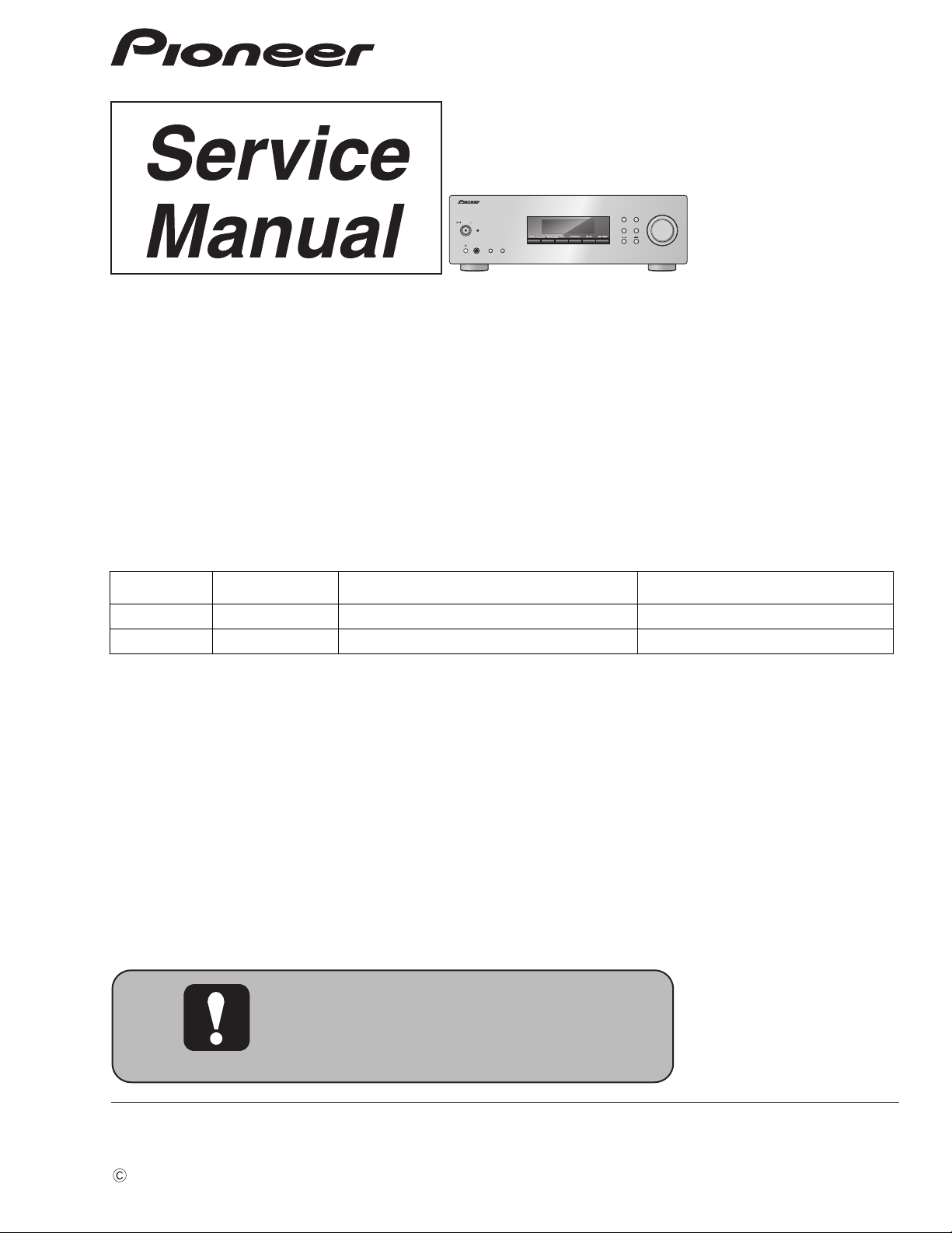
STEREO RECEIVER
SX-20
VOLUME
TUNE / PRESET
STANDBY ON
STANDBY
PHONES
A
SPEAKERS
B
SX-20-K
MEMORY
BALANCE
TONE
STEREO RECEIVER
SX-20-K
SX-20-S
THIS MANUAL IS APPLICABLE TO THE FOLLOWING MODEL(S) AND TYPE(S).
Model Type Power Requirement Remarks
SX-20-K YXE8 AC 220 V to 230 V
SX-20-S YXE8 AC 220 V to 230 V
ORDER NO.
RRV4392
K-ZZZ OCT.
2012 Printed in Japan

1
This service manual is intended for qualified service technicians; it is not meant for the casual do-ityourselfer. Qualified technicians have the necessary test equipment and tools, and have been trained
to properly and safely repair complex products such as those covered by this manual.
Improperly performed repairs can adversely affect the safety and reliability of the product and may
void the warranty. If you are not qualified to perform the repair of this product properly and safely, you
should not risk trying to do so and refer the repair to a qualified service technician.
2 3 4
SAFETY INFORMATION
A
B
CONTENTS
SAFETY INFORMATION..........................................................................................................................................................2
1. SERVICE PRECAUTIONS....................................................................................................................................................3
C
D
E
1.1 NOTES ON SOLDERING ...............................................................................................................................................3
1.2 SERVICE NOTICE..........................................................................................................................................................3
2. SPECIFICATIONS.................................................................................................................................................................4
3. BASIC ITEMS FOR SERVICE...............................................................................................................................................5
3.1 CHECK POINTS AFTER SERVICING............................................................................................................................5
3.2 PCB LOCATIONS ...........................................................................................................................................................6
4. BLOCK DIAGRAM.................................................................................................................................................................8
4.1 OVERALL WIRING DIAGRAM .......................................................................................................................................8
4.2 SIGNAL BLOCK DIAGRAM..........................................................................................................................................10
4.3 LEVEL and POWER SUPPLY BLOCK DIAGRAM .......................................................................................................12
4.4 GND MAP DIAGRAM....................................................................................................................................................14
5. DIAGNOSIS.........................................................................................................................................................................16
5.1 TROUBLESHOOTING..................................................................................................................................................16
5.2 DETECTION CIRCUIT..................................................................................................................................................22
5.3 IC INFORMATION.........................................................................................................................................................23
6. SERVICE MODE .................................................................................................................................................................33
6.1 SERVICE MODE...........................................................................................................................................................33
6.2 FACTORY DEFAULT SETTINGS .................................................................................................................................36
7. DISASSEMBLY ...................................................................................................................................................................37
8. EACH SETTING AND ADJUSTMENT ................................................................................................................................43
9. EXPLODED VIEWS AND PARTS LIST...............................................................................................................................44
9.1 PACKING SECTION .....................................................................................................................................................44
9.2 EXTERIOR SECTION...................................................................................................................................................46
10. SCHEMATIC DIAGRAM....................................................................................................................................................50
10.1 MAIN ASSY (1/2) ........................................................................................................................................................50
10.2 MAIN ASSY (2/2) ........................................................................................................................................................52
10.3 FRONT, LED, POWER SW. SPK SW AB, RMC and HP ASSYS...............................................................................54
11. PCB CONNECTION DIAGRAM.........................................................................................................................................56
11.1 MAIN ASSY.................................................................................................................................................................56
11.2 FRONT, POWER SW, HP, LED, RMC, SPK SW AB, GUIDE C and GUIDE R ASSYS..............................................60
12. PCB PARTS LIST..............................................................................................................................................................64
F
2
1
2 3 4
SX-20-K

5
• For environmental protection, lead-free solder is used on the printed circuit boards mounted in this unit.
Be sure to use lead-free solder and a soldering iron that can meet specifications for use with lead-free solders for repairs
accompanied by reworking of soldering.
• Compared with conventional eutectic solders, lead-free solders have higher melting points, by approximately 40 ºC.
Therefore, for lead-free soldering, the tip temperature of a soldering iron must be set to around 373 ºC in general, although
the temperature depends on the heat capacity of the PC board on which reworking is required and the weight of the tip of
the soldering iron.
Do NOT use a soldering iron whose tip temperature cannot be controlled.
Compared with eutectic solders, lead-free solders have higher bond strengths but slower wetting times and higher melting
temperatures (hard to melt/easy to harden).
The following lead-free solders are available as service parts:
• Parts numbers of lead-free solder:
GYP1006 1.0 in dia.
GYP1007 0.6 in dia.
GYP1008 0.3 in dia.
• Discharging
For more detail, please refer to "7. DISASSEMBLY - 1. Discharging".
6 7 8
1. SERVICE PRECAUTIONS
1.1 NOTES ON SOLDERING
A
B
1.2 SERVICE NOTICE
C
D
E
SX-20-K
5
6 7 8
F
3
1
Amplifier section
Power output specification is for when power supply is
230 V.
• Continuous power output
(both channels driven at 20 Hz to 20 kHz)
100 W+100 W (THD 1 %, 8 Ω)
Audio section
• Input (Sensitivity/Impedance)
SACD/CD . . . . . . . . . . . . . . . . . . . . . . . . . . . 400 mV/47 kΩ
PHONO (MM) . . . . . . . . . . . . . . . . . . . . . . . 5.5 mV/47 kΩ
• Output (Level/Impedance)
RECORDER OUT. . . . . . . . . . . . . . . . . . . . 400 mV/2.0 kΩ
• Frequency response
SACD/CD, NETWORK, RECORDER
. . . . . . . . . . . . . . . . . . . . . . . . . . . . 5 Hz to 100 kHz dB
PHONO (MM) . . . . . . . . . . . . . . 20 Hz to 20 kHz ±0.5 dB
• Tone control
(When VOLUME is set to –30 dB)
Bass . . . . . . . . . . . . . . . . . . . . . . . . . . . . ± 14 dB (100 Hz)
Treble . . . . . . . . . . . . . . . . . . . . . . . . . . . ± 14 dB (10 kHz)
• Signal-to-Noise Ratio (IHF SHORTED,
A-NETWORK)
SACD/CD, NETWORK, RECORDER . . . . . . . . . . . 100 dB
PHONO (MM, 5.5 mV input) . . . . . . . . . . . . . . . . . .80 dB
• Total Harmonic Distortion
SACD/CD, NETWORK, RECORDER . . . . . 0.01 % or less
(1 kHz, 50 W, 8 Ω)
• Speaker load impedance
A, B. . . . . . . . . . . . . . . . . . . . . . . . . . . . . . . . . . 4 Ω to 16 Ω
A+B . . . . . . . . . . . . . . . . . . . . . . . . . . . . . . . . . 8 Ω to 16 Ω
Tuner Section
Frequency Range (FM) . . . . . . . . . .87.5 MHz to 108 MHz
Antenna Input (FM). . . . . . . . . . . . . . . . 75 Ω unbalanced
Frequency Range (AM). . . . . . . . . . . 531 kHz to 1602 kHz
Antenna (AM) . . . . . . . . . . . . . . . . . . . . . . . Loop antenna
Miscellaneous
Power requirements . . . .AC 220 V to 230 V, 50 Hz/60 Hz
Power consumption . . . . . . . . . . . . . . . . . . . . . . . . 210 W
In standby . . . . . . . . . . . . . . . . . . . . . . . . . . . . . . . 0.3 W
Dimensions
. . . . . . . . . . . 435 mm (W) x 142.5 mm (H) x 364 mm (D)
Weight (without package) . . . . . . . . . . . . . . . . . . . 8.3 kg
Accessories
• Accessories
Remote control . . . . . . . . . . . . . . . . . . . . . . . . . . . . . . . . . 1
AAA/IEC R03 dry cell batteries . . . . . . . . . . . . . . . . . . . . 2
AM loop antenna. . . . . . . . . . . . . . . . . . . . . . . . . . . . . . . .1
FM wire antenna . . . . . . . . . . . . . . . . . . . . . . . . . . . . . . . . 1
Power cord
Warranty card
Quick start guide
Safety Brochure
Operating instructions (CD-ROM)
Note
• Specifications and the design are subject to
possible modifications without notice, due to
improvements.
• Corporation and product names mentioned herein
are trademarks or registered trademarks of the
respective corporations.
Remote Control
(8300764700010-IL)
AAA size IEC R03 dry cell batteries x2
AM loop antenna
(E601019000010-IL)
Power cord
(L068250160020-IL)
Warranty card
CD-ROM (Operating instructions)
(6517000001020-IL)
SX-20
-K/-S
FM wire antenna
(E605010140010-IL)
Quick start guide
(5707000007450-IL)
Safety Brochure
(5227000002540-IL)
2. SPECIFICATIONS
A
2 3 4
B
C
D
E
F
4
1
2 3 4
SX-20-K
5
Item to be checked regarding audio
Distortion
Noise
Volume too low
Volume too high
Volume fluctuating
Sound interrupted
To keep the product quality after servicing, confirm recommended check points shown below.
See the table below for the items to be checked regarding audio.
No. Procedures Check points
1
Check the symptom pointed out by a customer The pointed content should not reoccur
Sound and operation should not be defective
2
Check each input and main VOL (check the
operation of selector)
The sound is output by selecting an analog-connected input
with a selector and the sound volume should change by
rotating main VOL knob
3
Check the tone control, balance, and function The sound quality or right and left balances should change
by rotating each VOL knob
4
Check DIRECT functions The tone control should be disabled by setting DIRECT
function to ON.
6 Check SPEAKER A/B and headphone terminal There should not be defect in sound such
5 Check the tuner (AM and FM) operations Audio and operations must be normal.
as noise
7
Check the external package Check scratch or taint is not generated after accepting the
repair
6 7 8
3. BASIC ITEMS FOR SERVICE
3.1 CHECK POINTS AFTER SERVICING
A
B
C
D
E
F
SX-20-K
5
6 7 8
5
1
FRONT ASSY
MAIN ASSY
A
B
RMC ASSY
F
LED ASSY
E
SPK SW AB ASSY
G
GUIDE R ASSY POWER SW ASSY
C
HP ASSY
D
GUIDE C
ASSY
NSP 1..PCB TTL ASSY MAIN 7025HK1204010-IL
2..MAIN ASSY 7028072771010-IL
NSP 1..PCB TTL ASSY FRONT 7025HK1204011-IL
2..FRONT ASSY 7028072761010-IL
2..LED ASSY 7028072762010-IL
2..POWER SW ASSY 7028072763010-IL
2..SPK SW AB ASSY 7028072764010-IL
2..RMC ASSY 7028072765010-IL
2..HP ASSY 7028072766010-IL
2..GUIDE C ASSY 7028072767010-IL
2..GUIDE R ASSY 7028072768010-IL
Mark No. Description Part No. Mark No. Description Part No.
LIST OF ASSEMBLIES
NOTES: - Parts marked by “NSP” are generally unavailable because they are not in our Master Spare Parts List.
-
The > mark found on some component parts indicates the importance of the safety factor of the part.
Therefore, when replacing, be sure to use parts of identical designation.
3.2 PCB LOCATIONS
A
2 3 4
B
C
D
E
F
6
1
2 3 4
SX-20-K

5
6 7 8
A
B
C
D
E
F
SX-20-K
5
6 7 8
7
1
B
FRONT ASSY
(7028072761010-IL)
(7028072771010-IL)
MAIN ASSY
A
1/2 -(
A
2/2 )
A
2 3 4
4. BLOCK DIAGRAM
4.1 OVERALL WIRING DIAGRAM
A
B
C
D
E
F
8
1
2 3 4
SX-20-K
5
G
SPK SW AB ASSY
(7028072764010-IL)
C
POWER SW ASSY
(7028072763010-IL)
E
LED ASSY
(702807276
2010-IL)
F
RMC ASSY
(702807276
5010-IL)
D
HP ASSY
(7028072766010-IL)
6 7 8
A
B
C
D
E
F
SX-20-K
5
6 7 8
9
1
B
FRONT ASSY
MAIN ASSY
A
IC605
IC601
IC101
FLT400
IC400
IC700
IC105
IC104
IC103
IC106
PACK101
4.2 SIGNAL BLOCK DIAGRAM
A
B
2 3 4
C
D
E
F
10
SX-20-K
1
2 3 4
5
IC502
IC503
IC301
6 7 8
A
B
C
D
E
F
SX-20-K
5
6 7 8
11
1
AC 0.20A
S3(FLT)
DC 0.4A
S2(+15V,-15V)
DC3.95A
S1(AMP B+/B-)
SUB
TRANS
AC CORD
MAIN
TRANS
POWER DIAGRALEVEL DIAGRAM
IC605
IC700
IC601
2 3 4
4.3 LEVEL and POWER SUPPLY BLOCK DIAGRAM
A
B
C
D
E
F
12
SX-20-K
1
2 3 4
5
AC 0.20A
S3(FLT)
DC 0.4A
1N4007
1N4007
1SS133T
1N4007
1N4007
1SS133T
1/50
ST_BY RLY
MTZ2.4B
S2(+15V,-15V)
DC3.95A
S1(AMP B+/B-)
POWER_DOWN
MTZJ5.6B
RESET
SUB
TRANS
MAIN
TRANS
6 7 8
A
B
C
D
5
SX-20-K
6 7 8
E
F
13
1
GND map
BACK CHASSI
ST3.3V
V+15V
V+15V
V+15VV+9V
GND_A
GND_D
VREF
V-15V
BLUE
RED
ST3.3V
ST3.3V
WIRE403B
(CHGND)
WIRE401
(NM)
WIRE402
(NM)
C425(NM)
R466(NM)
C417(NM)
C140(NM)
C141(22uF)
C142(NM)
C143(22uF)
C402(0.1uF)
C403(0.1uF)
C413(0.1uF)
C449(0.1uF)
C131(22uF)
C134(NM)
C121(10uF)
C130(100uF)
eala
TONE
Function/E.Vol IC
E.VOL
D402(NM)
D403(NM)
R459(NM)
R218(100 ohm)
R215(100 ohm)
Pre Amp
(+16dB)
C436(NM)
R403(NM)
WIRE402
(CHGND)
AC from Main Trans
FL
FL uCOM
CPU/
EEPROM
ST3.3V
ST3.3V
V+15V
V+15V
C167
(10uF)
C166
(10uF)
T/OUT_+5V
V-15V
REFERENCE
POINT
V+6V
V-6V
J367(NM)
J369(NM)
J370(NM)
J159(NM)
J311(0 ohm)
SACD/CD
NETWORK
REC_IN
REC_OUT
PHONO
TUNER
BD109
(NM)
R804(0 ohm)
J393(0 ohm)
C713(0.022uF)
C715 (NM)
Screw
(CHGND)
Screw
(CHGND)
Screw
(CHGND)
Screw
(CHGND)
C132R(NM)
C707R(47uF)
C132L(NM)
C707L(47uF)
GW1 GND
(NM)
V-30V
(for FL)
D407(KDS4148)
D406(KDS4148)
C713 (0.01uF)
MAIN ASSY
A
D
HP ASSY
C
POWER SW ASSY
E
LED ASSY
F
RMC ASSY
G
SPK SW
AB ASSY
B
FRONT ASSY
IC400
IC102
IC101
IC700
IC103
IC106
IC105
IC601
IC605
J301(0 ohm)
J373(0 ohm)
4.4 GND MAP DIAGRAM
A
2 3 4
B
C
D
E
F
14
1
SX-20-K
2 3 4
5
V+24V
(for RELAY)
+- +-
+-
+-
V+24V
(for RELAY)
+- +-
+-
+-
V+24V
(for RELAY)
V+15V
V+B
V+B
V+15V
V-B
V-B
3V3
AC
RELAY
V-30V
3V3
PROTECTION
CIRCUIT
V-15V
A_GND
S_GND
C551(NM)
C509(6800uF)
C510(6800uF)
C542(0.047uF)
C303
(470uF)
C308
C524(NM)
C525(NM)
J272(0 ohm)
J363(0 ohm)
C550(0 ohm)
GND101
(CHGND)
GND401
(CHGND)
C331(10uF)
C711(NM)
C712(NM)
R332A
(NM)
C318R
(0.047uF)
R331A
(NM)
C318L
(0.047uF)
GT6
(CHGND)
GT7
(CHGND)
J116
(0 ohm)
J392
(0 ohm)
SP_B_Rch
SP_A_Rch
SP_A_Lch
SP_B_Lch
C342L/R(100uF)
C343L/R (NM)
C344L/R(100uF)
C345L/R(330pF)
C340L/R(100uF)
C341L/R (NM)
C513
(220uF)
C517
(1000uF)
C530
(100uF)
C536
(470uF)
C502
(47uF)
V+24V
(for RELAY)
V+3V
(for MUTE)
V+3V
(for MUTE)
MUTE
CIRCUIT
Power Amp
(+27dB)
V+24V
(for RELAY)
R463(NM)
CHGND
S_GND(Power AMP)
A_GND(±15V)
A_GND(Relay)
CPU GND(subtrans)
A_GND(TUNER)
D_GND(Protection)
S_GND(HEADPHONE)
S_GND(PHONO)
C418(0.022uF)
D404(NM)
D405(NM)
WIRE400
(CHGND)
S2
S1
Main Trans
Sub Trans
ASSY
IC301
IC503
IC502
6 7 8
A
B
C
D
5
SX-20-K
6 7 8
E
F
15
1
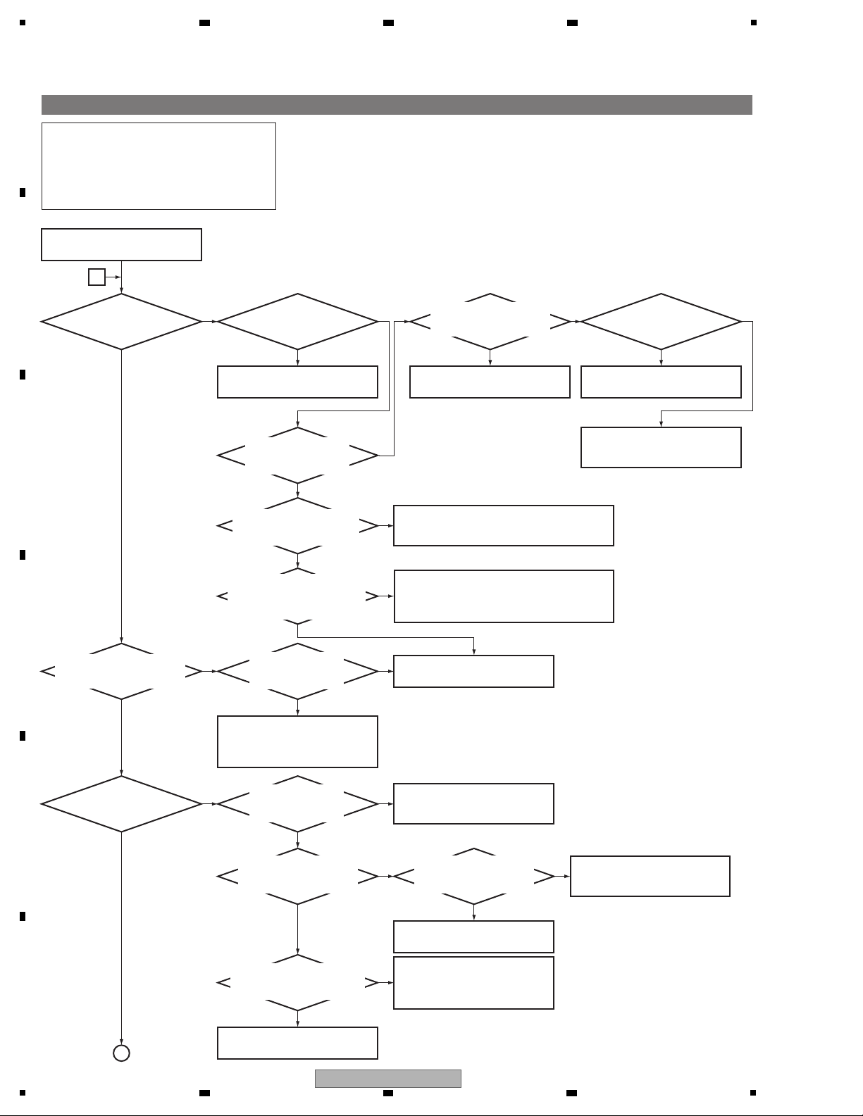
Is power ON?
When pressed the "STANDBY/ON"
button of the remote control unit, is
there remote control signal wave?
(Check the R270.)
Does the STANDBY LED
lit?
Is the "POWER_DOWN" line
Low (DC0V)?
(Check the J361.)
Is a DC wave
(rectification waveform DC +8V)
in the D516 cathode side?
Is there DC +3.3V
in 3V3 line?
(Check the J361 (3V3).)
Ye s
Ye s
No
After power ON, does
Protection Relay (RLY501) do
ON? (sound occurs click)
Does the sound
output from RECORDER OUT
terminal?
Is there DC +3.3V
in FL_SW/RLY line?
(Check the J182.)
Ye s
Ye s
Ye s
Ye s
Ye s
Ye s
No
Is there DC+9.0V
in +9V line?
(Check the J152.)
Is there signal
in IC605 pin 6/pin 27?
(Check the C114L/R + pin.)
Is the voltage of
REC_MUTE 0 V?
(Check the J310 REC_MUTE.)
Is there signal
in IC605 pin 1/pin 32?
(Check the C103L/R + pin.)
No
No
No
No
Speaker_A No sound
[Product state]
• Power cord connection (230 V/50 Hz)
• Unit POWER SW: ON
• Power ON operation by remote control
• SPEAKER-A selection
• INPUT: SACD/CD
A sound does not come out
from Speaker_A.
A protection circuit works.
(See "6. SERVICE MODE".)
No
No
Ye s
Ye s
Ye s
Ye s
IC301 is defective or its solder is
defective.
IC101 is defective or its solder is
defective.
Is a AC wave
in the D516 anode side?
Ye s
D516 to D519 are defective
or Those solders are defective.
• D515 or D523 is defective or its solder is defective.
• DZ502 is defective or its solder is defective.
• Q300 is defective or its solder is defective.
• REM401 is defective or its solder is defective.
• Connection between CN403 - CP403 is defective.
• Connection between CN402 - CP402 is defective.
• Connection between FPC400 - FPC101 is defective.
No
No
• IC104 is defective or its solder is
defective.
• Check the +15 V power supply.
• Q552 or Q553 is defective or its
solder is defective.
• Q551 is defective or its solder is
defective.
IC605 is defective or communication
defective or its solder is defective.
Ye s
IC101 is defective or its solder is
defective.
No
• JACK102 solder is defective.
• C103L or C103R solder is
defective.
No
No
No
• F101 is defective.
• T502 is defective or its solder is
defective.
• RLY501 is defective or its solder
is defective.
• Q502 is defective or its solder is
defective.
I
a
5. DIAGNOSIS
5.1 TROUBLESHOOTING
A
B
2 3 4
C
D
E
F
16
1
2 3 4
SX-20-K
5
Is there DC+15V in IC601 pin 8?
(Check the C141 + pin.)
Is there DC-15V in IC601 pin 4?
(Check the C143 - pin.)
Is there signal
in IC601 pin 3/pin 5?
(Check the C122L/R - pin.)
Is there signal
in IC601 pin 1/pin 7?
(Check the C601L/R + pin.)
Ye s
Ye s
Ye s
Is there signal
in Power Amp input?
(Check the J335, J336.)
Is there signal
in Power Amp output?
(Check the J122 L_HOT,
J124 FR_HOT.)
Is the voltage of
MAIN_MUTE 0 V?
(Check the J317 MAIN_MUTE.)
Ye s
Is SPK-A/RLY High?
(Check the R199
SPK-A/RLY.)
Ye s
Is SPK-B/RLY High?
(Check the R200
SPK-B/RLY.)
Ye s
Ye s
Ye s
Ye s
No
No
No
No
IC101 is defective or its solder is
defective.
IC101 is defective or its solder is
defective.
No
IC101 is defective or its solder is
defective.
• IC605 is defective or communication
defective or its solder is defective.
• C122L/R solder is defective.
No
• Q314L/R, Q316, Q317 are defective
or those solders are defective.
• Q315 is defective or its solder is
defective.
• C601L/R solder is defective.
No
• R218 or R215 is defective or its
solder is defective.
• Check the ±15 V power supply.
• Power Amp block is defective .
• Check a solder of Power Amp block.
•
RLY302 is defective or its solder is
defective.
•
Q314 is defective or its solder is
defective.
Ye s
•
RLY301 is defective or its solder is
defective.
•
Q313 is defective or its solder is
defective.
No
• IC601 is defective or its solder is
defective.
• D1000 to D1003 are defective or
those solders are defective.
• Q107 or Q113 is defective or its
solder is defective.
a
Speaker_B No sound
[Product state]
• Power cord connection (230 V/50 Hz)
• Unit POWER SW: ON
• Power ON operation by remote control
• SPEAKER-B selection
• INPUT: SACD/CD
Does a sound come
out from Speaker_A?
No
See "Speaker_A No Sound".
A sound does not come out
from Speaker_B.
I
6 7 8
A
B
C
D
E
F
SX-20-K
5
6 7 8
17
1
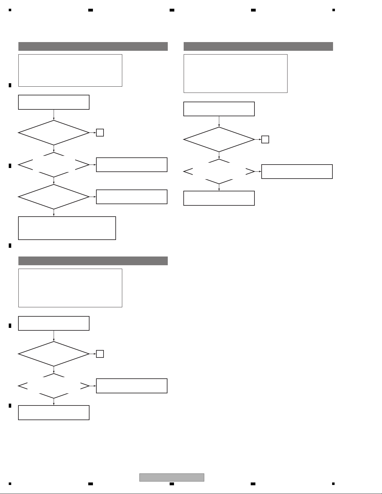
Is H/P_RLY High?
(Check the J107 H/P_RLY.)
Ye s
Ye s
No
IC101 is defective or its solder is
defective.
No
R343L or R343R is defective or its
solder is defective.
Ye s
• RLY301 is defective or its solder is defective.
• Q313 is defective or its solder is defective.
• Connection of CP301 is defective.
• JACK401 is defective or its solder is defective.
Phones No sound
[Product state]
• Power cord connection (230 V/50 Hz)
• Unit POWER SW: ON
• Power ON operation by remote control
• INPUT: SACD/CD
Does a sound come
out from Speaker_A?
No
See "Speaker_A No Sound".
A sound does not come out
from phones.
I
Is there signal in
RLY303?
(Check the R343L/R.)
Ye s
Ye s
No
• JACK102 solder is defective.
• C106L or C106R solder is defective.
IC605 is defective or communication
defective or its solder is defective.
NETWORK No sound
Does a sound come
out from SACD/CD input?
No
See "Speaker_A No Sound".
A sound does not come out
from NETWORK input.
I
Is there signal in
IC605 pin 2/pin 31?
(Check the C106L/R + pin.)
[Product state]
• Power cord connection (230 V/50 Hz)
• Unit POWER SW: ON
• Power ON operation by remote control
• SPEAKER-A selection
• INPUT: NETWORK
Ye s
Ye s
No
• JACK101 solder is defective.
• C109L or C109R solder is defective.
IC605 is defective or communication
defective or its solder is defective.
RECODER IN No sound
Does a sound come
out from SACD/CD input?
No
See "Speaker_A No Sound".
A sound does not come out
from RECODER input.
I
Is there signal in
IC605 pin 3/pin 30?
(Check the C109L/R + pin.)
[Product state]
• Power cord connection (230 V/50 Hz)
• Unit POWER SW: ON
• Power ON operation by remote control
• SPEAKER-A selection
• INPUT: RECODER IN
A
2 3 4
B
C
D
E
F
18
SX-20-K
1
2 3 4
Ye s
Ye s
No
No
No
• JACK103 solder is defective.
• C703L or C703R solder is defective.
No
IC605 is defective or communication
defective or its solder is defective.
Ye s
IC605 is defective or communication
defective or its solder is defective.
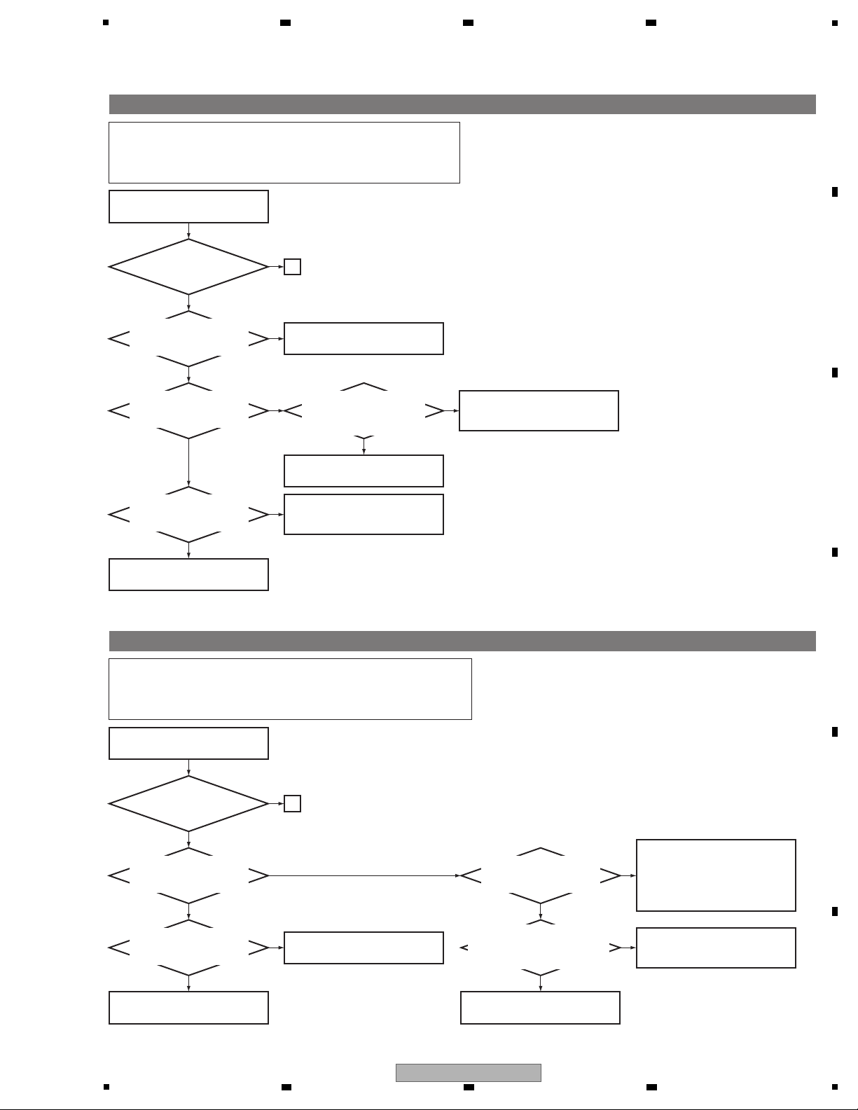
PHONO No sound
Does a sound come
out from SACD/CD input?
No
See "Speaker_A No Sound".
A sound does not come out
fromPHONO input.
I
Is there signal in
IC700 pin 3/pin 5?
(Check the C703L/R + pin.)
Ye s
Is there signal in
IC605 pin 4/pin 29?
(Check the C710L/R + pin.)
Ye s
Ye s
Is there signal in
IC700 pin 1/pin 7?
(Check the C708L/R + pin.)
Is there
DC+6V
in IC700 pin 8?
(Check the R708R.)
Is there
DC-6V
in IC700 pin 4?
(Check the R708L.)
[Product state]
• Power cord connection (230 V/50 Hz)
• Unit POWER SW: ON
• Power ON operation by remote control
• SPEAKER-A selection
• INPUT: PHONO
[Product state]
• Power cord connection (230 V/50 Hz)
• Unit POWER SW: ON
• Power ON operation by remote control
• SPEAKER-A selection
• INPUT: TUNER (FM/AM)
• Tuner setting: FM
• IC105 or IC106 is defective or its
solder is defective.
• Check the ±15 V power supply.
• IC101 is defective or its solder is
defective.
• PACK101 solder is defective.
No
C708L, C708R, C710L, C710R
are defective or those solders are
defective.
IC700 is defective or its solder is
defective.
PACK101 is defective or its solder is
defective.
C113L or C113R is defective or its
solder is defective.
Ye s
Ye s
Ye s
Ye s
No
No
TUNER No sound
Does a sound come
out from SACD/CD input?
No
See "Speaker_A No Sound".
A sound does not come out
from TUNER input.
I
Is there signal in
PACK101 pin 7/pin 8?
(Check the C113L/R - pin.)
Is there signal in
IC605 pin 5/pin 28?
(Check the C113L/R + pin.)
Is there DC+5V in PACK101
pin 5? (Check the R708R
for +6 V, R708L for -6 V.)
Is there communication waveform
in TUNER_SCLK and TUNER_SDIO?
(Check the J405 for TUNER_SCLK,
J406 for TUNER_SDIO.)
No
• IC103 is defective or its solder is
defective.
• BD121 solder is defective.
• D520 is defective or its solder is
defective.
• Check the ±15 V power supply.
5
6 7 8
A
B
C
D
5
6 7 8
SX-20-K
E
F
19
1
Ye s
Ye s
Ye s
Ye s
Ye s
Ye s
Ye s
No
• Connection of CP401 is defective.
• Main transformer is defective.
• FPC101 or FPC400 solder is defective.
• Connection between FPC101 - FPC400 is defective.
Ye s
Ye s
Ye s
Ye s
• FPC101 or FPC400 solder is defective.
• Connection between FPC101 - FPC400 is defective.
• FPC101 or FPC400 solder is defective.
• Connection between FPC101 - FPC400 is defective.
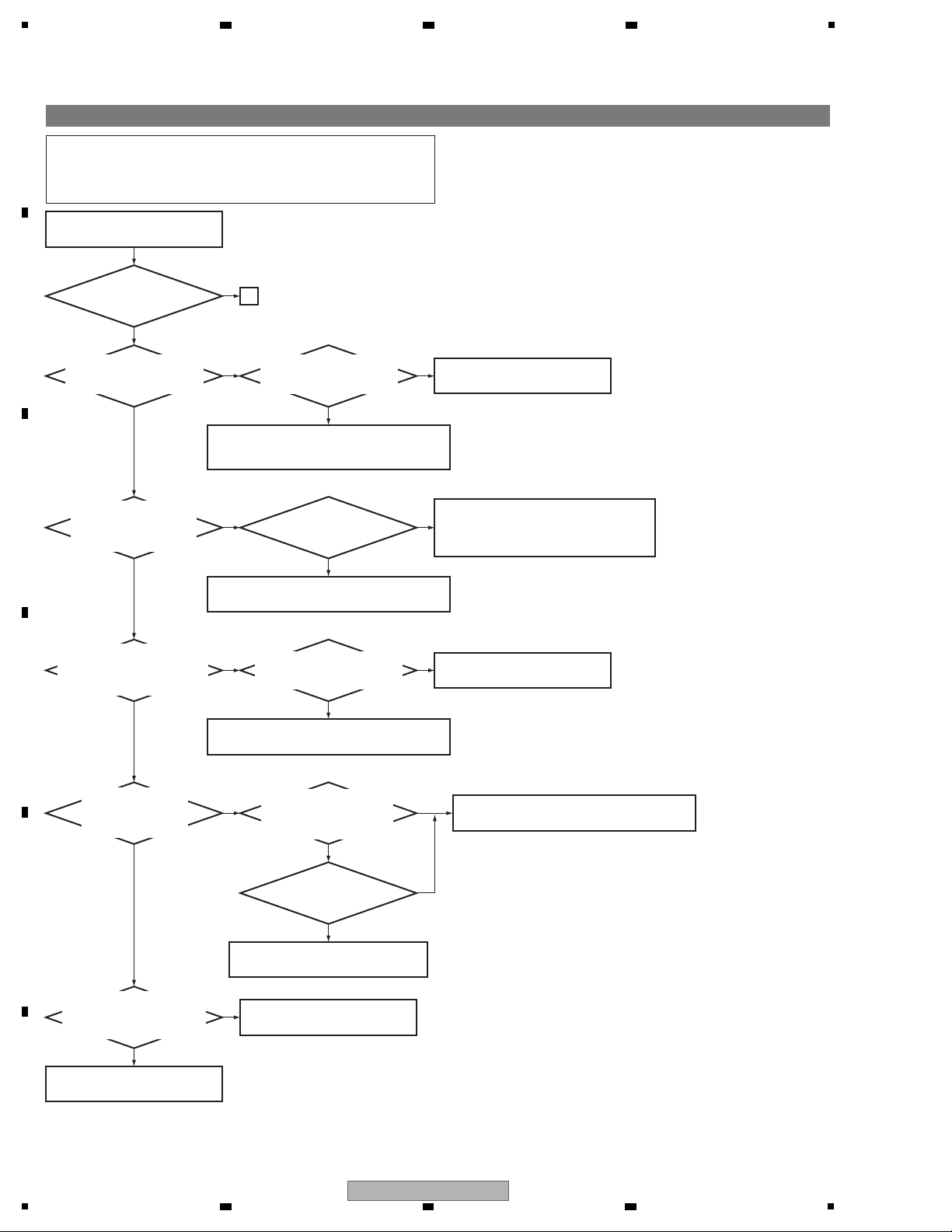
FL No light
Does a sound come
out from SACD/CD input?
No
No
No
No
See "Speaker_A No Sound".
FL does not light.
I
Is there AC waveform
signal in FLT pin 1/pin 39?
(Check the FRONT Assy side B.)
Is there DC-30V in
FRONT Assy -30V?
(Check the FPC400 pin 1
on FRONT Assy side B.)
Is there DC+3.3V in
IC400 VDD?
(Check the VDD on
FRONT Assy side B.)
Is there communication
waveform signal in
FLT pin 4 - pin 36?
(Check the FRONT Assy side B.)
Is there communication waveform in
FRONT Assy FL_CLK, FL_DOUT?
(Check the FL_CLK, FL_DOUT
on FRONT Assy side B.)
Is there DC-30V
in MAIN Assy -30V?
(Check the J304.)
No
No
No
Is there communication waveform
in MAIN Assy FL_CLK, FL_DOUT?
(Check the FPC101 pin 9/pin 10.)
No
Is there DC+3.3V in
FRONT Assy
FL_SW/RLY
?
(Check the
FPC400 pin 15
on
FRONT Assy side B.)
Does the STADBY LED
(Red) light at standby state?
Is there AC waveform
signal in R400A/R403A?
(Check the FRONT Assy side B.)
[Product state]
• Power cord connection (230 V/50 Hz)
• Unit POWER SW: ON
• Power ON operation by remote control
• SPEAKER-A selection
• INPUT: SACD/CD
IC101 is defective or its solder is
defective.
No
IC400 is defective or its solder is
defective.
FLT400 is defective or its solder is
defective.
• Q401 is defective or its solder is defective.
• Q402 is defective or its solder is defective.
• R400A or R403A is defective or its solder is defective.
• R404 or R405 is defective or its solder is defective.
• DZ400 is defective or its solder is defective.
• Q501 is defective or its solder is defective.
• DZ513 is defective or its solder is defective.
• R508 is defective or its solder is defective.
• FPC101 or FPC400 solder is defective.
A
B
2 3 4
C
D
E
F
20
1
2 3 4
SX-20-K
 Loading...