

Page 1
2007
MIC
FADER START
HEAD PHONES
VIDEO INPUT
USB
DVD
CH 1
VIDEO
EX
CH 4
MIC OFF ON
TALK
OVER
MIN
DVD/LINE PHONO
MAX
VIDEO
VIDEO
S-VIDEO
EX
VIDEO TRIM
MIC 1
MIC1
LEVEL
MIC2
LEVEL
HI
LOW
CH1
AUDIO INPUT
AUDIO TRIM
dB
OVER
10
7
4
2
1
0
–1
–2
–3
–5
–7
–10
–15
–24
+9
MID
+6-26
HI
+6-26
LOW
CUE
CROSS FADER
ASSIGN
PROFESSIONAL SOUND&VISION MIXER
BA
SVM-1000
+6-26
10
9
8
7
6
5
4
3
2
1
0
A THRU B
1
VIDEO INPUT
DVD
MIN
DVD LINE DIGITAL
MAX
VIDEO
S-VIDEO
VIDEO TRIM
AUDIO INPUT
AUDIO TRIM
dB
OVER
10
7
4
2
1
0
–1
–2
–3
–5
–7
–10
–15
–24
+9
MID
+6-26
HI
+6-26
LOW
CUE
CROSS FADER
ASSIGN
+6-26
10
9
8
7
6
5
4
3
2
1
0
A THRU B
2
VIDEO INPUT
DVD
MIN
DVD LINE DIGITAL
MAX
VIDEO
S-VIDEO
VIDEO TRIM
AUDIO INPUT
CH SELECT
AUDIO TRIM
dB
OVER
10
7
4
2
1
0
–1
–2
–3
–5
–7
–10
–15
–24
+9
MID
+6-26
HI
+6-26
LOW
CUE
CROSS FADER
ASSIGN
+6-26
10
9
8
7
6
5
4
3
2
1
0
CROSS FADER CURVE SD CARD
A THRU B
3
dB
OVER
10
7
4
2
1
0
–1
–2
–3
–5
–7
–10
–15
–24
VIDEO INPUT
DVD
MIN
LINE PHONO
MAX
VIDEO
VIDEO
S-VIDEO
VIDEO TRIM
AUDIO INPUT
AUDIO TRIM
dBLR
OVER
10
7
4
2
1
0
–1
–2
–3
–5
–7
–10
–15
–24
+9
BOOTH MONITOR
0
MID
+6-26
HI
+6-26
LOW
CUE
CROSS FADER
ASSIGN
+6-26
BALANCE
MASTER
RL
CUE
10
9
8
7
6
5
4
3
2
1
0
CH FADER CURVE
VIDEO
MASTER LEVEL
WHITEBLACK
MONO STEREO
A THRU B
4
EX
0
0
0
+12
-12
+12-12
CH2
CH3
CH4
MONOSPLIT STEREO
MIXING
PHONES
MASTER
CUE
LEVEL
AUDIO MASTER LEVEL
0
TIME/
PARAMETER
LEVEL/
DEPTH
EFFECT
CUE
VIDEO FX
PATTERN/
TEXT BANK
MAXMIN
FADER
AV SYNC
VIDEO
SOLO MODE
JPEG
VIEWER
ON/OFF
SET UP
VIDEO EQ
MASTER
MONITOR
SET UP
UTILITY
EFFECT
ON/OFF
2
4
5
6
7
SVM-1000
For details, refer to "Important Check Points for good servicing".
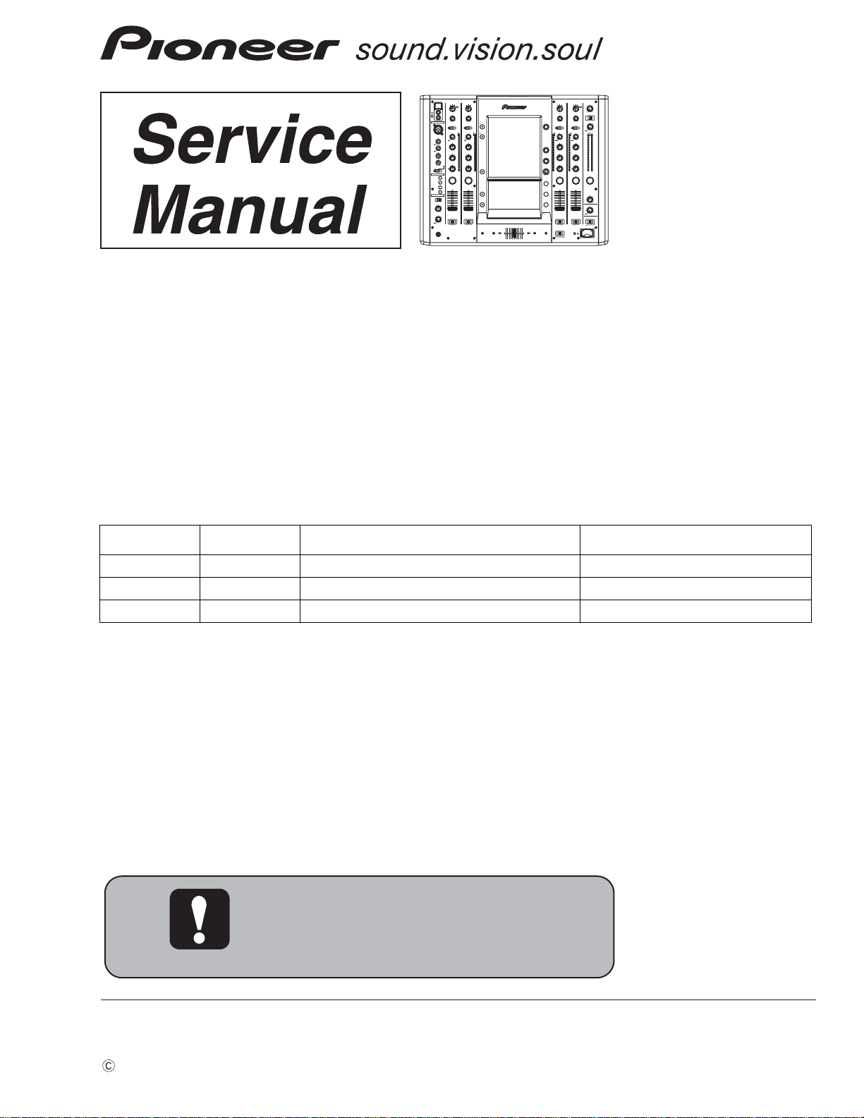
SOUND & VISION MIXER
SVM-1000
THIS MANUAL IS APPLICABLE TO THE FOLLOWING MODEL(S) AND TYPE(S).
Model Type Power Requirement Remarks
SVM-1000 KUCXJ AC 120 V
SVM-1000 WYXJ5 AC 220 V to 240 V
SVM-1000 TLXJ AC 110 V to 240 V
ORDER NO .
RRV3678
PIONEER CORPORATION 4-1, Meguro 1-chome, Meguro-ku, Tokyo 153-8654, Japan
PIONEER ELECTRONICS (USA) INC. P.O. Box 1760, Long Beach, CA 90801-1760, U.S.A.
PIONEER EUROPE NV Haven 1087, Keetberglaan 1, 9120 Melsele, Belgium
PIONEER ELECTRONICS ASIACENTRE PTE. LTD. 253 Alexandra Road, #04-01, Singapore 159936
PIONEER CORPORATION
T-ZZR DEC.
2007 Printed in Japan
Page 2
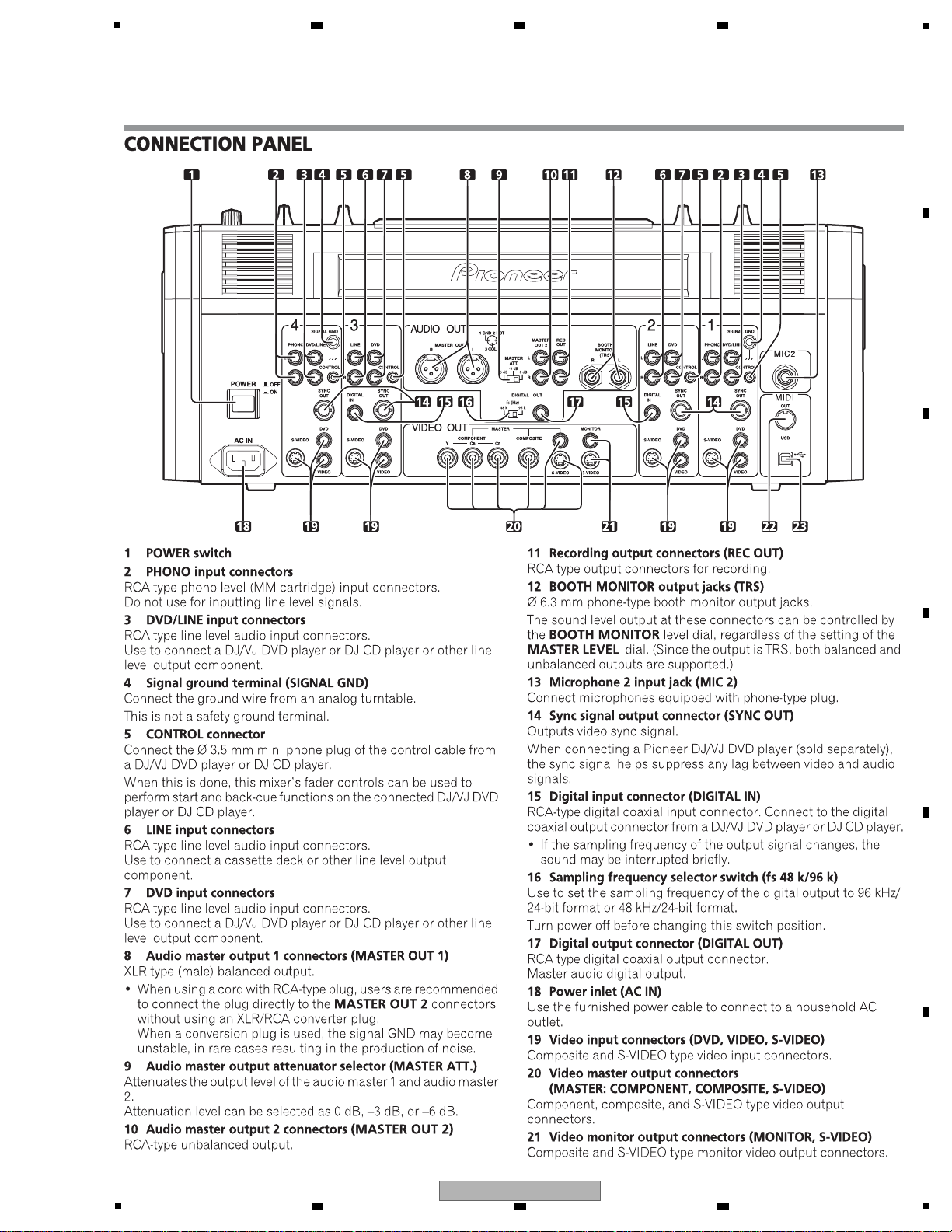
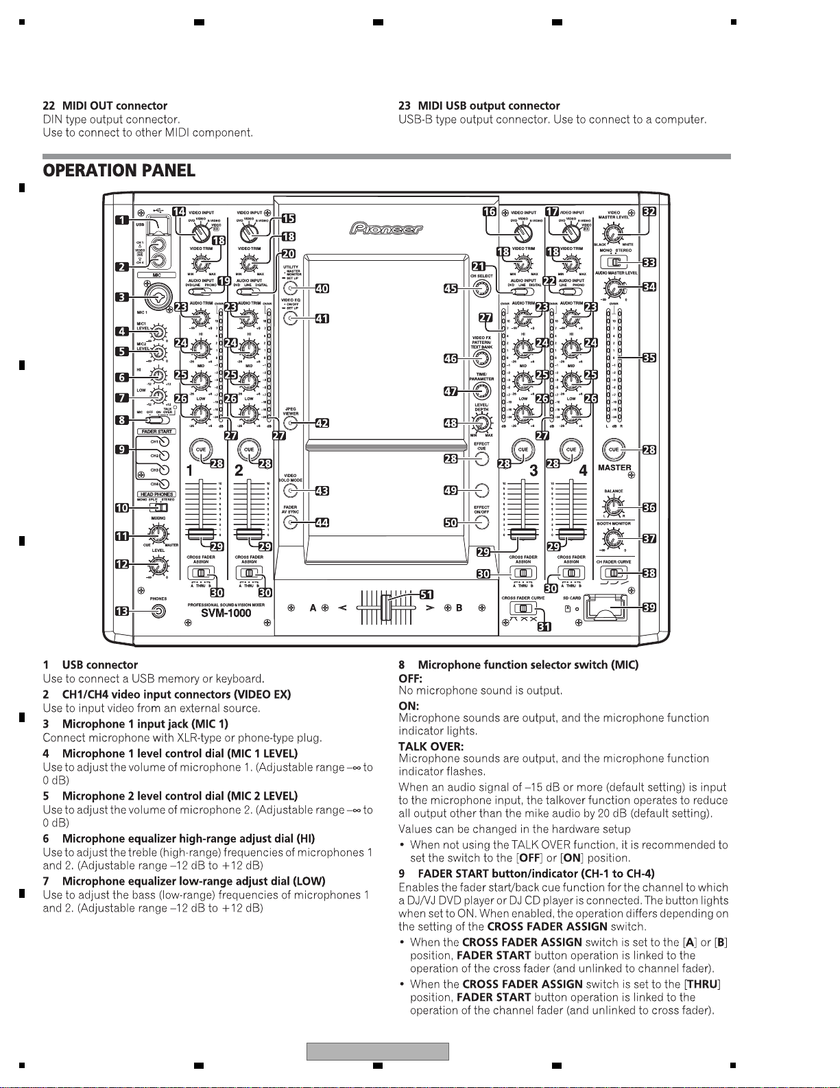
1
1. SAFETY PRECAUTIONS
The following check should be performed for the
continued protection of the customer and service
technician.
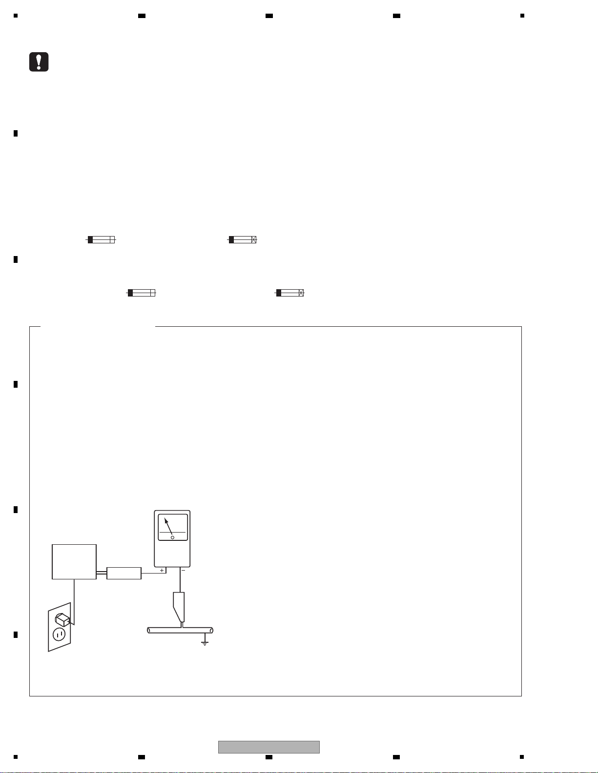
LEAKAGE CURRENT CHECK
Measure leakage current to a known earth ground
(water pipe, conduit, etc.) by connecting a leakage
current tester such as Simpson Model 229-2 or
equivalent between the earth ground and all exposed
metal parts of the appliance (input/output terminals,
screwheads, metal overlays, control shaft, etc.). Plug
the AC line cord of the appliance directly into a 120V
AC 60 Hz outlet and turn the AC power switch on. Any
current measured must not exceed 0.5 mA.
ANY MEASUREMENTS NOT WITHIN THE LIMITS
OUTLINED ABOVE ARE INDICATIVE OF A POTENTIAL
SHOCK HAZARD AND MUST BE CORRECTED BEFORE
RETURNING THE APPLIANCE TO THE CUSTOMER.
2. PRODUCT SAFETY NOTICE
Many electrical and mechanical parts in the appliance
have special safety related characteristics. These are
often not evident from visual inspection nor the protection
afforded by them necessarily can be obtained by using
replacement components rated for voltage, wattage, etc.
Replacement parts which have these special safety
characteristics are identified in this Service Manual.
Electrical components having such features are
identified by marking with a > on the schematics and on
the parts list in this Service Manual.
The use of a substitute replacement component which
does not have the same safety characteristics as the
PIONEER recommended replacement one, shown in the
parts list in this Service Manual, may create shock, fire,
or other hazards.
Product Safety is continuously under review and new
instructions are issued from time to time. For the latest
information, always consult the current PIONEER Service
Manual. A subscription to, or additional copies of,
PIONEER Service Manual may be obtained at a nominal
charge from PIONEER.
Leakage
current
tester
Reading should
not be above
0.5 mA
Device
under
test
Test all
exposed metal
surfaces
Also test with
plug reversed
(Using AC adapter
plug as required)
Earth
ground
AC Leakage Test
(FOR USA MODEL ONLY)
WARNING
This product contains lead in solder and certain electrical parts contain chemicals which are known to the state of California to
cause cancer, birth defects or other reproductive harm.
Health & Safety Code Section 25249.6 - Proposition 65
NOTICE
(FOR CANADIAN MODEL ONLY)
Fuse symbols (fast operating fuse) and/or (slow operating fuse) on PCB indicate that replacement parts must
be of identical designation.
REMARQUE
(POUR MODÈLE CANADIEN SEULEMENT)
Les symboles de fusible (fusible de type rapide) et/ou (fusible de type lent) sur CCI indiquent que les pièces
de remplacement doivent avoir la même désignation.
This service manual is intended for qualified service technicians ; it is not meant for the casual
do-it-yourselfer. Qualified technicians have the necessary test equipment and tools, and have been
trained to properly and safely repair complex products such as those covered by this manual.
Improperly performed repairs can adversely affect the safety and reliability of the product and may
void the warranty. If you are not qualified to perform the repair of this product properly and safely, you
should not risk trying to do so and refer the repair to a qualified service technician.
2 3 4
SAFETY INFORMATION
A
B
C
D
E
F
2
1
2 3 4
SVM-1000
Page 3

5
6 7 8
(FOR USA MODEL ONLY)
This product contains mercury. Disposal of this material may be regulated due to environmental considerations.
For disposal or recycling information, please contact your local authorities or the Electronics Industries
Alliance: www.eiae.org.
The backlighting lamp of LCD in this equipment contains mercury. Disposal of this material may be
regulated due to environmental considerations according to Local, State or Federal Laws. For disposal
or recycling information, please contact your local authorities or the Electronics Industries
Alliance: www.eiae.org
A
B
C
D
E
F
SVM-1000
5
6 7 8
3
Page 4
1
2 3 4
[Important Check Points for Good Servicing]
In this manual, procedures that must be performed during repairs are marked with the below symbol.
Please be sure to confirm and follow these procedures.
A
1. Product saf ety
Please conform to product regulations (such as safety and radiation regulations), and maintain a safe servicing environment b y
following the safety instructions described in this manual.
1 Use specified parts for repair.
Use genuine parts. Be sure to use important parts for safety .
2 Do not perform modifications without proper instructions.
Please follow the specified safety methods when modification(addition/change of parts) is required due to interferences such as
radio/TV interference and foreign noise .
B
C
D
3 Make sure the soldering of repaired locations is properly performed.
When you solder while repairing, please be sure that there are no cold solder and other debris.
Soldering should be finished with the proper quantity . (Refer to the e xample)
4 Make sure the screws are tightly fastened.
Please be sure that all screws are fastened, and that there are no loose screws .
5 Make sure each connectors are correctly inserted.
Please be sure that all connectors are inserted, and that there are no imperfect insertion.
6 Make sure the wiring cables are set to their original state.
Please replace the wiring and cables to the original state after repairs.
In addition, be sure that there are no pinched wires, etc.
7 Make sure screws and soldering scraps do not remain inside the product.
Please check that neither solder debris nor screws remain inside the product.
8 There should be no semi-broken wires , scratches, melting, etc. on the coating of the pow er cord.
Damaged power cords may lead to fire accidents, so please be sure that there are no damages .
If you find a damaged power cord, please exchange it with a suitab le one.
9 There should be no spark traces or similar marks on the power plug.
When spark traces or similar marks are found on the power supply plug, please check the connection and advise on secure
connections and suitable usage. Please exchange the po wer cord if necessary .
a Safe en vironment should be secured during servicing.
When you perform repairs, please pay attention to static electricity, furniture, household articles, etc. in order to prev ent injuries.
Please pay attention to your surroundings and repair safely.
2. Adjustments
T o k eep the original performance of the products, optimum adjustments and confirmation of characteristics within specification.
Adjustments should be performed in accordance with the procedures/instructions described in this manual.
3. Lubricants, Glues , and Replacement parts
Use grease and adhesives that are equal to the specified substance.
E
Make sure the proper amount is applied.
4. Cleaning
For parts that require cleaning, such as optical pickups, tape deck heads, lenses and mirrors used in projection monitors, proper
cleaning should be performed to restore their performances.
5. Shipping mode and Shipping scre ws
T o protect products from damages or f ailures during transit, the shipping mode should be set or the shipping screws should be
installed before shipment. Please be sure to follo w this method especially if it is specified in this manual.
F
4
1
SVM-1000
2 3 4
Page 5

5
6 7 8
CONTENTS
SAFETY INFORMATION......................................................................................................................................2
1. SERVICE PRECAUTIONS................................................................................................................................7
1.1 NOTES ON SOLDERING......................................................... .......................................... ........................7
2. SPECIFICATIONS.............................................................................................................................................7
2.1 ACCESSORIES..........................................................................................................................................7
2.2 SPECIFICATIONS ......................................................................................................................................8
2.3 PANEL FACILITIES........................................................ .......................................... ...................................9
3. BASIC ITEMS FOR SERVICE........................................................................................................................13
3.1 CHECK POINTS AFTER SERVICING .................................................................... .................................13
3.2 PCB LOCATION ..................................................................................... ..................................................14
4. BLOCK DIAGRAM..........................................................................................................................................16
4.1 OVERALL WIRING DIAGRAM ......................................... .......................................... ..............................16
4.2 AUDIO BLOCK DIAGRAM............................................................................................... .........................18
4.3 VIDEO BLOCK DIAGRAM.................................. ... .......................................... .........................................20
4.4 FUNCTION BLOCK DIAGRAM ................................................................................................................22
5. DIAGNOSIS....................................................................................................................................................24
5.1 DIAGNOSIS FLOW.......................................................................................... .........................................24
5.2 POWER ON SEQUENCE............................................................................. ............................................25
6. SERVICE MODE.............................................................................................................................................27
6.1 LIST OF PAGES IN SERVICE MODE.............................. .......................................... ..............................27
6.2 SERVICE MODE........................................................... ... .......................................... ..............................27
6.3 SERVICE MODE IDENTIFICATION .........................................................................................................28
6.4 LIST OF PAGES IN TEST MODO ............................................................................................ ................33
6.5 TEST MODE.......................................................... .. .......................................... .......................................34
6.6 TEST MODE IDENTIFICATION................................................................................................................35
6.7 HOW T O USB DOWNLOAD................................................................... ... ...............................................41
6.8 NOTES ON VARIOUS SETTINGS WHEN THE UNIT ARE REPLACED............................................... ..43
7. DISASSEMBLY ...............................................................................................................................................44
8. EACH SETTING AND ADJUSTMENT............................................................................................................55
9. EXPLODED VIEWS AND PARTS LIST...........................................................................................................56
1 PACKING SECTION........................................................................................................... ......................56
9.
9.2 EXTERIOR SECTION .................................................................................. ............................................58
9.3 BOTTOM SECTION................................................. .......................................... .......................................60
9.4 OPERATION PANEL SECTION............................................................................................. ...................62
9.5 LCD PANEL SECTION ..................................................... .......................................... ..............................64
10. SCHEMATIC DIAGRAM............................................. .. ................................................ ... ... ...........................66
10.1 AUD1 ASSY (1/5)...................................................................................................................................66
10.2 AUD1 ASSY (2/5)...................................................................................................................................68
10.3 AUD1 ASSY (3/5)...................................................................................................................................70
10.4 AUD1 ASSY (4/5)...................................................................................................................................72
10.5 AUD1 ASSY (5/5)...................................................................................................................................74
10.6 AUD2 ASSY (1/5)...................................................................................................................................76
10.7 AUD2 ASSY (2/5)...................................................................................................................................78
10.8 AUD2 ASSY (3/5)...................................................................................................................................80
10.9 AUD2 ASSY (4/5)...................................................................................................................................82
10.10 A
10.11 VIO1 ASSY...........................................................................................................................................86
10.12 MJCK, VIN3 and VIO2 ASSYS.............................................................................................................88
10.13 MAIN ASSY (1/9). .................................................................................................................................90
10.14 MAIN ASSY (2/9). .................................................................................................................................94
10.15 MAIN ASSY (3/9). .................................................................................................................................98
10.16 MAIN ASSY (4/9). ...............................................................................................................................102
10.17 MAIN ASSY (5/9). ...............................................................................................................................106
10.18 MAIN ASSY (6/9). ...............................................................................................................................110
10.19 MAIN ASSY (7/9). ...............................................................................................................................114
10.20 MAIN ASSY (8/9). ...............................................................................................................................118
10.21 MA
10.22 SCPU ASSY (1/2)...............................................................................................................................126
10.23 SCPU ASSY (2/2)...............................................................................................................................130
10.24 CTL1 ASSY ........................................................................................................................................134
10.25 CTL2A ASSY......................................................................................................................................136
10.26 CTL2B, CFD1, CFD2, CFD3 and CFD4 ASSYS................................................................................138
10.27 INVT ASSY.........................................................................................................................................140
10.28 CTL3R ASSY......................................................................................................................................142
UD2 ASSY (5/5) .................................................................................................................................84
IN ASSY (9/9)................................................................................................................................122
A
B
C
D
E
F
SVM-1000
5
6 7 8
5
Page 6

1
2 3 4
10.29 CTL3LB ASSY...................................................................................................................................144
10.30 CTL3LA, CRFD and DIO2 ASSYS.....................................................................................................146
10.31 DIO1 ASSY (1/2)................................................................................................................................148
10.32 DIO1 ASSY (2/2)................................................................................................................................150
A
10.33 MIDI ASSY......................................................................................................................................... 152
10.34 SDIO ASSY........................................................................................................................................ 154
10.35 USB1 and USB2 ASSYS ...................................................................................................................156
10.36 HAMP ASSY......................................................................................................................................158
10.37 MJCK and ACSW ASSYS.................................................................................................................. 160
10.38 PDIV ASSY........................................................................................................................................162
10.39 REG and ILMR ASSYS...................................................................................................................... 164
10.40 ILML ASSY ........................................................................................................................................ 166
10.41 POWER SUPPLY UNIT......................................................................................................................168
10.42 VOLTAGES......................................................................................................................................... 170
10.43 WAVEFORMS....................................................................................................................................173
11. PCB CONNECTION DIAGRAM................................................................................................................. 186
B
11.1 AUD1 and MJCK ASSYS..........................................................................................................
11.2 AUD2 ASSY......................................................................................................................................... 190
11.3 VIO1 and VIO2 ASSYS........................................................................................................................ 194
11.4 MAIN ASSY ......................................................................................................................................... 198
11.5 SCPU and CRFD ASSYS....................................................................................................................202
11.6 CTL1, CFD1 and CFD2 ASSYS...........................................................................................................206
11.7 CTL2A, CFD3, CFD4 and CTL2B ASSYS........................................................................................... 210
11.8 INVT, CTL3R, CTL3LB and CTL3LA ASSYS....................................................................................... 214
11.9 DIO2, SDIO, USB1 and USB2 ASSYS................................................................................................ 218
11.10 DIO1 and MIDI ASSYS...................................................................................................................... 220
11.11 ACSW, PDIV and REG ASSYS ......................................................................................................... 224
C
11.12 VIN3, ILMR and ILML A
SSYS ...........................................................................................................226
11.13 HAMP and HJCK ASSYS..................................................................................................................228
12. PCB PARTS LIST....................................................................................................................................... 230
........... 186
D
E
F
6
1
2 3 4
SVM-1000
Page 7

5
• For environmental protection, lead-free solder is used on the printed circuit boards mounted in this unit.
Be sure to use lead-free solder and a soldering iron that can meet specifications for use with lead-free solders for repairs
accompanied by reworking of soldering.
• Compared with conventional eutectic solders, lead-free solders have higher melting points, by approximately 40 °C.
Therefore, for lead-free soldering, the tip temperature of a soldering iron must be set to around 373 °C in general, although
the temperature depends on the heat capacity of the PC board on which reworking is required and the weight of the tip of
the soldering iron.
Compared with eutectic solders, lead-free solders have higher bond strengths but slower wetting times and higher melting
temperatures (hard to melt/easy to harden).
The following lead-free solders are available as service parts:
• Parts numbers of lead-free solder:
GYP1006 1.0 in dia.
GYP1007 0.6 in dia.
GYP1008 0.3 in dia.
• Operating Instructions
(KUCXJ: DRB1421)
(WYXJ5: DRB1422)
(TLXJ: DRB1423)
Accessories
• Power Cord
(KUCXJ : DDG1028)
(WYXJ5 : ADG7062)
(TLXJ : ADG7062)
• Warranty Card
6 7 8
1. SERVICE PRECAUTIONS
1.1 NOTES ON SOLDERING
A
B
2. SPECIFICATIONS
2.1 ACCESSORIES
C
D
E
5
SVM-1000
6 7 8
F
7
Page 8
1
Power source
KUCXJ model
. . . . . . . . . . . . . . . . . . . . . . . . . . . . . .
AC 120 V, 60 Hz
TLXJ model . . . . . . . . . . . . . . . . . . AC 110 V to 240 V, 50 Hz/60 Hz
WYXJ5 model
(Except SVM-1000/TLXJ)
2 3 4
2.2 SPECIFICATIONS
A
B
C
D
E
F
8
1
2 3 4
SVM-1000
Page 9
5
2.3 PANEL FACILITIES
6 7 8
A
B
C
D
E
F
SVM-1000
5
6 7 8
9
Page 10
1
A
B
2 3 4
C
D
E
F
10
1
2 3 4
SVM-1000
Page 11
5
6 7 8
A
B
C
D
E
F
SVM-1000
5
6 7 8
11
Page 12
1
A
B
2 3 4
C
D
E
F
12
1
2 3 4
SVM-1000
Page 13
5
6 7 8
3. BASIC ITEMS FOR SERVICE
3.1 CHECK POINTS AFTER SERVICING
To ensure the quality of the product after repair, check the recommended items shown below:
Item to be checkedProceduresNo.
A
Check if all the symptoms pointed out by the customer
1
have been addressed.
Check the analog audio inputs. (Make connections for
2
analog audio signals with a DVD player.)
Check the digital audio inputs. (Make connections for
3
digital audio signals with a DVD player.)
Check the video outputs.
4
(Make connections with a DVD player.)
5
Check the buttons.
6
Check the exterior section.10
The symptoms in question must not be reproduced.
Audio and operations must be normal.
Check the output of Audio Master Out connector 1 from all input connectors.
Check the outputs of the all output connectors from the CH1 input connector.
Audio for each channel and operations must be normal.
Input digital signals to CH2 and CH3 and check if the output signals from
the digital output connectors are normal.
Audio for each channel and operations must be normal.
Check the output of the Video Master Out connectors from all input connectors.
Check the outputs of the all output connectors from the CH1 input connector.
Video and operations must be normal.
Audio must be normal, without noise.Check the audio from headphone output.
Operate the buttons of the main unit, and check it operate normally.
Calibration must be terminated.Check the touch panel.7
The video system must be appropriately set for the destination.Check the System Setting.8
The content of utility setup must be the same as before the repair.Check the contents of utility setup.9
Check for any scratches or dirt that have been made or attached on
the exterior section after receiving the product for repair.
See the table below for the items to be checked regarding video and audio:
Item to be checked regarding video Item to be checked regarding audio
Block noise
Horizontal noise
Dot noise
Disturbed image (video jumpiness)
Too dark
Too bright
Mottled color
Distortion
Noise
Volume too low
Volume too high
Volume fluctuating
Sound interrupted
B
C
D
E
F
SVM-1000
5
6 7 8
13
Page 14
1
3.2 PCB LOCATION
Main Section
A
2 3 4
B
C
Front view
USB2 ASSY
Z
AG
VIN3 ASSY
E
ILML ASSY
ILMR ASSY
AF
3F
2F
MIDI ASSY
W
AUD1 ASSY
A
DIO1 ASSY
V
AUD2 ASSY
B
U
DIO2 ASSY
MJCK ASSY
D
1F
D
E
USB1 ASSY
Y
VIO1 ASSY
C
VIO2 ASSY
F
ACSW ASSY
AC
REG ASSY
AE
POWER SUPPLY UNIT
MAIN ASSY
G
F
14
1
2 3 4
SVM-1000
PDIV ASSY
AD
SDIO ASSY
X
Page 15
5
6 7 8
Operation Panel Section
Bottom view
CTL2A ASSY
J
CFD4 ASSY
CFD3 ASSY
O
N
CTL2B ASSY
K
SCPU ASSY
H
CRFD ASSY
T
CTL1 ASSY
I
HAMP ASSY
AA
CFD1 ASSY
L
CFD2 ASSY
M
HJCK ASSY
AB
INVT ASSY
P
CTL3R ASSY
Q
LCD Panel
CTL3LA
ASSY
S
CTL3LB
ASSY
R
A
B
C
NOTES: - Parts marked by “NSP” are generally unavailable because they are not in our Master Spare Parts List.
-
The > mark found on some component parts indicates the importance of the safety factor of the part.
Therefore, when replacing, be sure to use parts of identical designation.
Mark No. Description Part No. Mark No. Description Part No.
LIST OF ASSEMBLIES
1..MAIN ASSY DWX2715
NSP 1..SCIV ASSY DWM2302
2..SCPU ASSY DWX2706
2..INVT ASSY DWX2717
NSP 1..AUDI ASSY DWM2303
2..AUD1 ASSY DWX2718
2..DIO2 ASSY DWX2719
2..USB1 ASSY DWX2727
NSP 1..AUIL ASSY DWM2304
2..AUD2 ASSY DWX2721
2..ILMR ASSY DWX2722
2..ILML ASSY DWX2723
NSP 1..DIHP ASSY DWM2305
2..USB2 ASSY DWX2720
2..DIO1 ASSY DWX2724
2..PDIV ASSY DWX2725
2..HAMP ASSY DWX2726
2..SDIO ASSY DWX2728
2..MIDI ASSY DWX2751
2..REG ASSY DWX2767
2..COVER PCB DWX2793
NSP 1..CTVI ASSY DWM2306
2..CTL1 ASSY DWX2729
2..CTL3R ASSY DWX2730
2..VIO1 ASSY DWX2731
2..VIO2 ASSY DWX2732
2..VIN3 ASSY DWX2733
2..HJCK ASSY DWX2734
NSP 1..CTFD ASSY DWM2307
2..CTL2A ASSY DWX2735
2..CTL2B ASSY DWX2736
2..ACSW ASSY DWX2737
2..MJCK ASSY DWX2738
2..CRFD ASSY DWX2739
2..CFD1 ASSY DWX2740
2..CFD2 ASSY DWX2741
2..CFD3 ASSY DWX2742
2..CFD4 ASSY DWX2743
2..CTL3LA ASSY DWX2744
2..CTL3LB ASSY DWX2745
> 1..POWER SUPPLY UNIT DWR1440
> 1..LCD Panel CWX3405
D
E
F
SVM-1000
5
6 7 8
15
Page 16
1
3
MIC2
7
CH3
VIDEO SYNC
OUT
19
5
1
4
3
OUT DDEN
12
6
5
CN1016
AKM1277-
11
12
FADER_ST_4+
24
V+5D
1
8
3
17
GNDD
12
16
MUTE_OFF1
1
MUTE_OFF
13
CBV_CH1_1
GNDA
DIGI_4896_OUT
15
6
INPUT_SEL4
16
5
RST_HP
2
GNDD
1
GNDA
GNDD
13
GNDA
GPO_CH1START
2
+5V_USB1
7
CBV_CH1_2
GNDA
MAIN_YOUT
7
1
MUTE_OFF2
14
20
26
POWER SUPPLY
UNIT (DWR1440)
29
10
V-15
CH2
VIDEO
INPUT
GNDA
2
GNDD
7
GNDD
MASTER_DATA
4
3
96K_3
R
32
14
GNDA
MMCMD
L
15
DKP3792-
PH
4PIN
MIC_DATA
5
MIC_DATA
8
14
VR_CS_INPUT1
6
12
GNDA
+5V_USB1
GNDD
35
19
GNDA
TO SCPU
VR_CS0
30
CN5009
S7B-EH
ATT
24
16
GNDA
5
SDDAT3
7
16
VR_CS_INPUT2
1
8
5
2
CN7401
CKS4999-
12
6
12
33
9
GNDD
G
14
SWPS
16
SUB_S_YOUT
RSD_AAD
13
1
6
9
7
1
V-BB
G
GNDD
LRCK
+5V_USB2
MAIN_CROUT
DOUT_DATA
GNDA
22
GNDD
VR_SIR_SCK
2
MAIN_MIC_HOT
7
11
5
5
MASTER_DATA
10
VR_CS4
Y_CH3_1
MAIN_MIC_COLD
LRCK
37
GNDD
CH3
VIDEO
INPUT
12
LINE
GNDD
1
Y_CH4_1
GNDD
2
1
DIR_CS2
GNDD
TOP PANEL
CH4_DATA
13
SUB_VOUT
CLK24M_3
L
DSP_RST
4
GNDA
CN4011
DKN1512-
33
4
22
HP_DATA
22
BOOTH
MONITOR
(TRS)
8
96K_2
V-BB
GNDD
GNDD
24
CN8005
VKN1193-
FADER_ST_3+
GNDA
HP_DATA
12
LINE
GNDA
9
V+15
22
DIGITAL
IN
2
6
19
3
XCARDIN
GNDD
8
1
GNDA
26
DIGI_4896_OUT
CN5005
PLUG 19PIN
VKN1775-
22
GNDA
21
6
2
XCARDIN
CN1007
AKM1275-
GNDD
9
GNDD
1
GNDD
9
V+8
13
12
5
GNDD
17
CN1009
VKN1428-
11
L
34
DOUT_DATA
3
R
7
7
13
31
GNDD
LINE
XRESET
10
VR_DATA
17
6
28
1
6
8
15
GNDA
CN8202
S6B-PH-K-S
19
7
13
19
14
OUT DDT11
7
DIGITAL
OUT
V+12
10
DKP3791-
PH 6PIN
SHIELD
1
3
V+3R3
FPGA_TX
11
1
7
14
REC OUT
COMPONENT
2
GNDD
CBV_CH3_1
7
17
CN202
B15B-PH-K-S
CH3
AUDIO
CN6501
DKN1480-
XMMCD
GNDA
19
24
20
1
7
3
DVD
11
9
GNDA
CBV_CH4_2
CBV_CH4_3
V+5
2
CN7403
B4B-PH-K-S
5
MCK
4
CH3_DATA
8
29
CH2
MASTER OUT1
28
2
4
1
GNDD
8
VR_CS2
21
GNDD
GNDD
GNDD
24
1
GNDA
96K_2
CH3_DIGI_INPUT
Y_CH4_1
29
DIR_CS1
V+15A
CLK24M_2
GNDD
GNDA
5
GNDA
GNDA
OUT DDT9
VR_CLK
MAIN_S_DC
31
6
MUTE_OFF
4
D-_USB1
CN1012
VKN1434-
CBV_CH4_3
2
GNDD
11
11
5
TP1_YAD
151413
DDD1384-
1mm FFC 17PIN
REVERSE
13
GPO_CH4START
24
VR_CS_INPUT4
4
1
37
32
CN8651
B4B-PH-K-S
6
GNDA
16
GNDA
TP1_XV
GNDA
3
L
V+5D
VIDEO
SYNC
OUT
GNDD
2
C_CH1_1
GNDA
10
32
D+_USB1
9
2
GNDA
GNDD
SYNC_OUT
21
N
7
TO ILMR
RST_SRC
PF15PP-S17
C_CH3_1
10
1
PHON
17
PF07EE-D12
16
GNDD
V+5D
C_CH1_1
7
GND5
HP L
V+15
GNDA
3
SUB_S_YOUT
13
23
GNDA
4
V+5A
14
8
17
D+_USB1
GLED
GNDA
1
6
GNDD
29
12
OUT DDT10
7
7
27
GNDD
15
21
7
GNDD
2
GNDD
13
DDD1375-
1mm FFC 34PIN
REVERSE
6M_3
TO AUD2
1
16
3
23
1
2
CN1017
AKM1280-
V+15B
REC_DATA
33
GNDD
VR_CS5
3
V-BB
9
GNDD
GNDD
6
CONT
SDPOWER
SUB_S_DC
GNDA
MIDI_TX
7
CH1
AUDIO
GNDA
24
30
C_CH4_1
11
BOOTH_MUTE
12
GNDD
CH1_FADER
36
VR_CLK
DVD
7
1
19
MONITOR
5
34
GNDD
CH3_DATA
PF02EE-D32
18
CBV_CH2_1
21
1
1
12
18
8
24
GNDA
GNDD
MCK
24
9
DDD1381-
1mm FFC 30PIN
REVERSE
5
11
MAIN_CBOUT
27
GNDD
28
FROM PDIV
GNDA
OUT DDT13
GPO_CH3START
31
9
3
2
GNDD
GNDA
CN4016
RECEPTACLE 19PIN
19R-1.25FJ
19
22
40
C_CH2_1
1
5
SDWP
CH3_DIGI_INPUT
GNDA
20
5
GNDA
V-15
SDDAT3
5
12
GNDD
2
17
V+5D
MUTE_OFF1
GNDD
15
CN9157
B2B-EH
10
CN4014
S8B-EH
9
CN5004
PLUG 19PIN
VKN1775-
10
OUT DDT4
GNDD
GNDD
VR_SIR_RX
GNDA
17
5
12
MAIN_S_DC
VR_SIR_TX
1
C_CH2_1
GNDD
KUC DDG1028-
CBV_CH1_2
3
GNDFL
GNDA
6
C_CH4_1
MAIN_VOUT
S-VIDEO
GNDA
GNDA
CN8551
AKM1276-
CN7705
VKN1193-
V+5D
3
22
VR_CS3
5
V-15
JJ BDG1048-
29
14
CH4_DATA
CONT
23
GND15
4
3
CN
B2B
1
WY TL ADG7062-
3
GNDD
4
26
GND5
GNDD
GNDD
GND5
27
EFFECT_ON
CN4002
B3B-PH-K-S
GNDA
MASTER
GNDA
1
13
DIT_CS1
FADER_ST_1-
2
VR_SIR_TX
17
MUTE_OFF2
V+5D
V3R3
27
V+3R3DREF
CBV_CH3_2
18
CN1008
VKN1417-
CRS_FADER
CN4010
DKN1511-
MAIN_S_YOUT
15
S-VIDEO
13
SUB_S_COUT
R
OUT DDT12
25
7
7
5
4
GNDD
20GNDD
GNDD
INPUT_SEL3
8
FPGA_SCLK
7
GNDD
PWRFL(+15)
CN8301
VKN1305-
GNDD
3
4
6
V+15A
GNDA
MIDI_TX
MAIN_S_COUT
9
18
9
CBV_CH4_1
GNDA
CLK24M_3
22
11
VR_MUTE
CN9151
B5B-PH-K-S
2
CH3_DIGI_IN
INPUT_SEL3
GNDA
2
CN3
52492
30
SUB_CPU_BUSY
2
3
9
4
15
28
INPUT_SEL4
ATT
3
JH9201
51048-0400
3
!
GNDD
L
DDD1376-
1mm FFC 17PIN
REVERSE
JUMPER
9PIN
CH1
GNDA
6
8
CONT
10
17
AC INLET ASSY
!
8
GREF1
GNDA
GNDA
V+5D
BOOTH_DATA
4
OUT DDT3
REAR PANEL
17
GNDD
7
25
4
GNDA
GNDA
GNDA
CH2_DATA
INSEL1
L
Y_CH3_1
DDD1377 1mm FFC
12PIN
REVERSE
SD CARD
4
20
2
CH4
VIDEO SYNC
OUT
3
15
CH1_FADER
V+5A
GNDA
CH2_DIGI_IN
GNDA
GNDA
16
N
GNDD
7
BCK
GPO_CH1STOP
5
2
8
GNDD
17
15
23
12
18
GNDA
7
29
GNDD
GNDD
1
13
GNDFL
GNDD
GNDD
PF05EE-D37
GNDA
32
18
22
5
9
25
25
17
GNDA
29
GNDA
4
GNDD
CN1010
VKN1438-
GNDD
28
19
10
CH1_DATA
GPO_CH3STOP
R
GNDA
OUT DDT7
6
OUT DDT15
9
V+5A
19
8
15
VR_CS_MASTER
18
CN1004
VKN1444-
18
13
D-_USB1
FADER_ST_4-
10
MMCMD
32
MIDI_TX
6M_3
MCK
13
INSEL1
GNDD
GNDA
28
CN1006
AKM1276-
PF08EE-
D17
FADER_ST_4-
Y_CH2_1
5
GNDA
GNDD
INPUT_SEL4
GNDD
REC_DATA
6
1
4
4
15
5
14
V-15
9
21
C_CH3_1
24
VLED(+5)
PWRFL(+15)
GNDA
15
MAIN_YOUT
13
13
V+5
CH2
SUB_S_DC
33
TAP_SW
GNDD
2
5
Y
FSYNC
10
GNDD
12
25
6
OUT DDT1
8
V3R3
5
CBV_CH4_2
FADER_ST_2-
CBV_CH3_1
PHONO
8
8
10
3
20
GNDA
15
32
VMUTE
18
19
PF05PP-
D20
22
8
17
OUT DDT14
8
7
12
16
GNDA
BCK
INSEL2
GNDD
GNDD
3
15
7
19
GNDA
GPO_CH2STOP
GNDD
GNDD
2
GNDD
GNDA
FADER_ST_4+
MUTE_OFF2
8
3
CH1_FADER
GNDD
GNDD
BOARD TO BOARD
19PIN
9
GNDD
INSEL3
VLED(+5)
26
3
NEUTRAL
96K_1
30
FADER_ST_3+
GNDA
4
D+_USB2
CBV_CH3_1
11
PHONO
INSEL4
L
39
SDDAT0
SDDAT2
DDD1378-
1mm FFC 24PIN
REVERSE
DCLKO
23
9
CN9152
B15B-PH-K-S
DDD1379-
1mm FFC 34PIN
CBV_CH3_2
2
CBV_CH3_2
N
V+5
SYNC_OUT
DIT_CS1_X
9
4
28
GNDD
23
V3R3
V+5D
V+5D
GNDA
GREF1
23
MAIN_CROUT
8
GND5
17
4
27
VMUTE
4
CN8601
AKM1290-
GNDD
CN
S5
6
BCK
6
GNDD
DIGI_4896_IN
OUT DDT8
GNDD
VR_MUTE
10
5
7
8
L
21
BOOTH_DATA
CBV_CH3_2
GNDA
34
CH2_DATA
V+5D
27
DIGI_4896_IN
DSP_RST
8
GNDD
SDPOWER
CN8701
S3B-PH-K-S
2
GNDD
Y_CH1_1
12
GNDD
GNDD
GNDD
6
9
V+5D
R
WA ADG7105-
5
10
12
30
GNDA
25
VR_CS3
3
GNDA
LINE
4
AC POWER CORD
V+12
VR_CS1
INSEL3
CN8251
VKN1374-
16
1
18
15
5
!
6
5
13
3
GNDD
WYTL WA DKP3762-
1
CH4_DATA
38
CH3_DATA
8
13
19
17
CBV_CH4_2
!
1
7
GNDA
5
V3R3
3
6
34
34
CBV_CH1_3
2
R
GNDA
!
26
GNDA
9
4
CN1001
VKN1434-
9
!
14
3
CBV_CH4_3
19
GNDD
9
GPO_CH2START
19
3
17
2
27
GNDD
31
VR_MUTE
CH4_FADER
14
9
CBV_CH1_3
V-15
GNDD
V+15D
CN1002
VKN1416-
GNDD
CN4015
RECEPTACLE 19PIN
19R-1.25FJ
XRESET
CN7706
VKN2004-
4
VR_DATA
18
V+15
3
12
COMPOSITE
27
GNDD
7
GNDA
GNDA
34
16
VR_CS_INPUT3
2
18
20
3
DIR_CS2
27
GNDA
1
JUMPER
4PIN
GNDD
JH9151
51048-0900
DSP_RST
4
GNDD
2
24
3
MASTER_MUTE_OFF
4
GNDA
GNDD
11
8
GNDA
10
INPUT_SEL3
VSYNC
14
GNDD
4
GNDA
10
6M_1
12
DKP3794-
PH 3PIN
SHIELD
INPUT_SEL2
6
20
GNDD
GNDD
1
3
SYNC_OUTPUT
RST_SRC
11
8
10
11
V+BB
26
20
3
11
OUT DDT5
CN9154
B5B-EH
4
6
2
SDWP
3
5
CN1015
VKN1421-
CBV_CH3_1
16
26
16
10
HP L
GNDD
9
CH1
VIDEO
INPUT
8
6
V+8D
11
15
V+5A
6
14
MIDI OUT
OUT DDT6
26
REC_DATAREC_DATA
R
2
GNDD
V3R3
GNDHP
GNDA
5
CLK24M_2
25
36
GNDA
GNDD
2
20
5
GNDD
V-15
D-_USB2
FADER_ST_4-
GNDA
4
C_CH3_1
12
1
6
SDDAT2
4
28
26
GNDA
1
MAIN_S_COUT
VR_CS4
7
DDD13811mm FFC
13PIN
13
V+15D
VR_CS4
4
31
1
CBV_CH2_2
GNDD
INPUT_SEL1
9
GNDD
GNDD
CBV_CH2_2
23
4
18
2
GNDD
3
18
4
12
Y_CH4_1
23
14
GNDD
VR_SIR_RX
22
11
DKP3799-
2PIN
33
CBV_CH4_2
5
DDD1388-
1mm FFC
5PIN
REVERSE
8
4
3
VR_CLK
GNDD
GNDD
30
CN6503
52147-0410
GNDD
GNDA
V+BB
GNDD
1
5
V+3R3DREF
1
GNDA
AC POWER CORD
6
FADER_ST_1+
CN6
52492
29
30
FADER_ST_3-
GNDD
10
CH3_FADER
MIC1
16
4
VR_SIR_SCK
GNDA
AC INLET ASSY
3
23
VR_MUTE
8
PF07EE-D12
18
3
VR_DATA
KUC JJ DKP3761-
29
15
GNDD
10
27
3
2
38
5
GNDD
JH9501
51048-0900
5
CN1003
VKN1438-
18
20
3
GNDD
1
16
4
6
4
11
3
15
10
V+15B
GNDA
30
6
CN9101
2-178496-4
PF08EE-D30
D+_USB2
C_CH3_1
6
CBV_CH4_3
J9101
(BOARD-IN)
14
MAIN_MIC_HOT
FADER_ST_3-
17
TP1_YV
CLK24M_1
CH2
AUDIO
GLED
6M_2
C_CH4_1
4
CONT
Y_CH2_1
12
16
SUB_CPU_RST
GNDA
14
5
V+5
CH4_DATA
1
1
D-_USB2
5
GNDA
ATT
CBV_CH2_1
6M_2
CN201
B5B-PH-K-S
31
1
2
28
+5V_USB2
4
GNDD
12
13
USB B
1
Y_CH1_1
GNDD
16
3
CH4
AUDIO
INSEL2
2
MASTER
OUT2
GNDD
CH1
VIDEO
INPUT
GNDD
CN6502
VKN1374-
GNDA
GNDD
V+BB
8
11
23
25
33
Cb
2
FADER_ST_2+
3
13
GNDA
35
2
7
MUTE_OFF
VR_CS5
MASTER_DATA
GNDD
TO HAMP
GNDD
11
V+5D
CH2_FADER
CH3_DATA
MMCLK
14
1
11
GNDD
6
21
4
CH1_DATA
VR_CLK
GNDA
25
XRESET
!
FPGA_RX
CH4
VIDEO
INPUT
21
GNDD
2
2
GNDA
2
11
14
ATT
16
MAIN_MIC_COLD
SUB_S_COUT
VR_MUTE
USB A
2
3
OUT DDT2
9
GNDD
GNDD
4
CH3_DIGI_IN
3
GNDA
CN5006
S8B-EH
12
CN9156
B8B-EH
10
GPO_CH4STOP
14
Y_CH3_1
MAIN_CBOUT
GNDA
SDDAT1
L
GNDD
LRCK
6
8
Y_CH4_1
96K_3
4
5
2
5
20
MIDI_TX
GNDA
BOARD TO BOARD
19PIN
GNDA
23
BOOTH_MUTE
15
11
GNDD
30
16
2
21
V+5D
GNDD
14
5
GNDA
11
V+5D
4
VR_CS3
4
10
XMMCD
1
GNDD
4
V+5A
V+8D
26
11
FADER_ST_3+
FADER_ST_4+
24
MMCLK
GNDD
MAIN_S_YOUT
SUB_CPU_INT
SYNC_OUTPUT
17
GNDREF
DDD1382-
1mm FFC 30PIN
MUTE_OFF1
15
GNDD
VIDEO
SYNC
OUT
3
15
GNDHP
4
DDD1383-
1mm FFC 40PIN
C_CH4_1
2
CN9155
B9B-PH-K-S
GND15
OUT DDT0
PF05PP
-S15
MASTER_DATA
GNDA
10
CBV_CH1_1
GNDD
GNDD
GNDA
V+8
FADER_ST_3-
L
10
GND15
29
8
VR_DATA
GNDA
28
GNDA
MAIN_VOUT
PF09PP-
D05
SDDAT1
21
CN9153
B7B-EH
RST_HP
2
1
INL101
B2P3-VH
INSEL4
DIR_CS1
GNDA
17
GNDA
CH3
DIGITAL
IN
GNDD
GNDD
Cr
GND15
11
GNDD
1
2
22
2
9
CBV_CH4_1
VMUTE
40
39
GNDREF
1
CH4
VIDEO
INPUT
7
GNDA
BROWN
1
V+15B
GNDD
9
GNDD
TP1_XAD
VR_CS5
5
25
WHITE
Y_CH3_1
1
V-15
6
SDDAT0
CN7707
VKN1200-
CH2_DIGI_IN
GNDA
19
6
21
V+15B
GNDD
LIVE
5
GNDD
SUB_VOUT
VR_CS_MIC
30
13
14
2
3
GNDD
CN101
Y
USB1 ASSY
(DWX2727)
D
HAMP ASSY
(DWX2726)
HJCK ASSY
(DWX2734)
MJCK A
(DWX27
Z
USB2 ASSY
(DWX2720)
B B( 1/5- 5/5)
B
AUD2 ASSY
(DWX2721)
A A( 1/5- 5/5)
A
AUD1 ASSY
(DWX2718)
G G( 1/9- 9/9)
G
MAIN ASSY
(DWX2715)
V V( 1/2- 2/2)
V
DIO1 ASSY
(DWX2724)
AA
AB
C
VIO1 ASSY
(DWX2731)
F
VIO2 ASSY
(DWX2732)
E
VIN3 ASSY
(DWX2733)
W
MIDI ASSY
(DWX2751)
U
DIO2 ASSY
(DWX2719)
X
SDIO ASSY
(DWX2728)
REG ASSY
(DWX2767)
AE
PDIV ASSY
(DWX2725)
AD
ACSW ASSY
(DWX2737)
AC
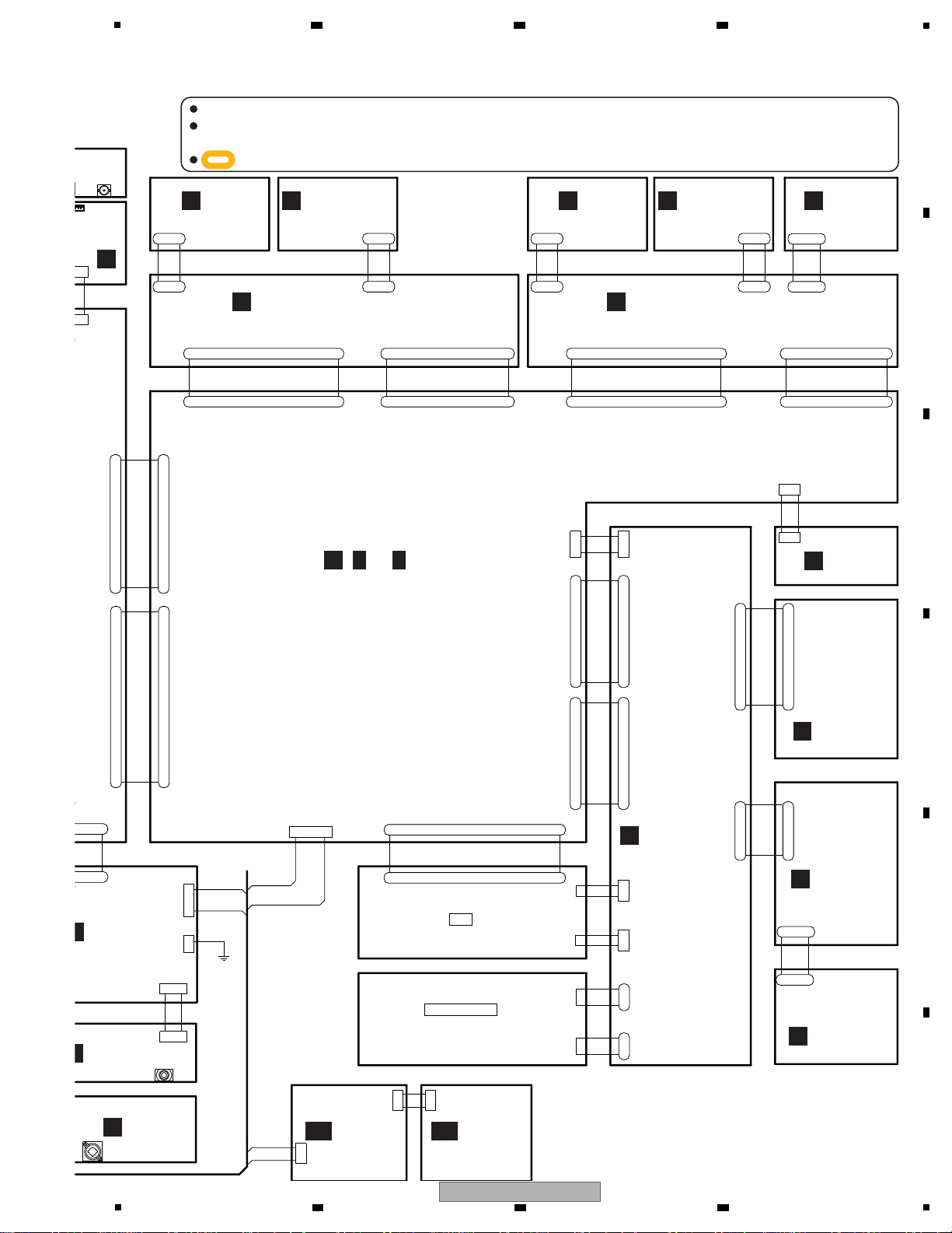
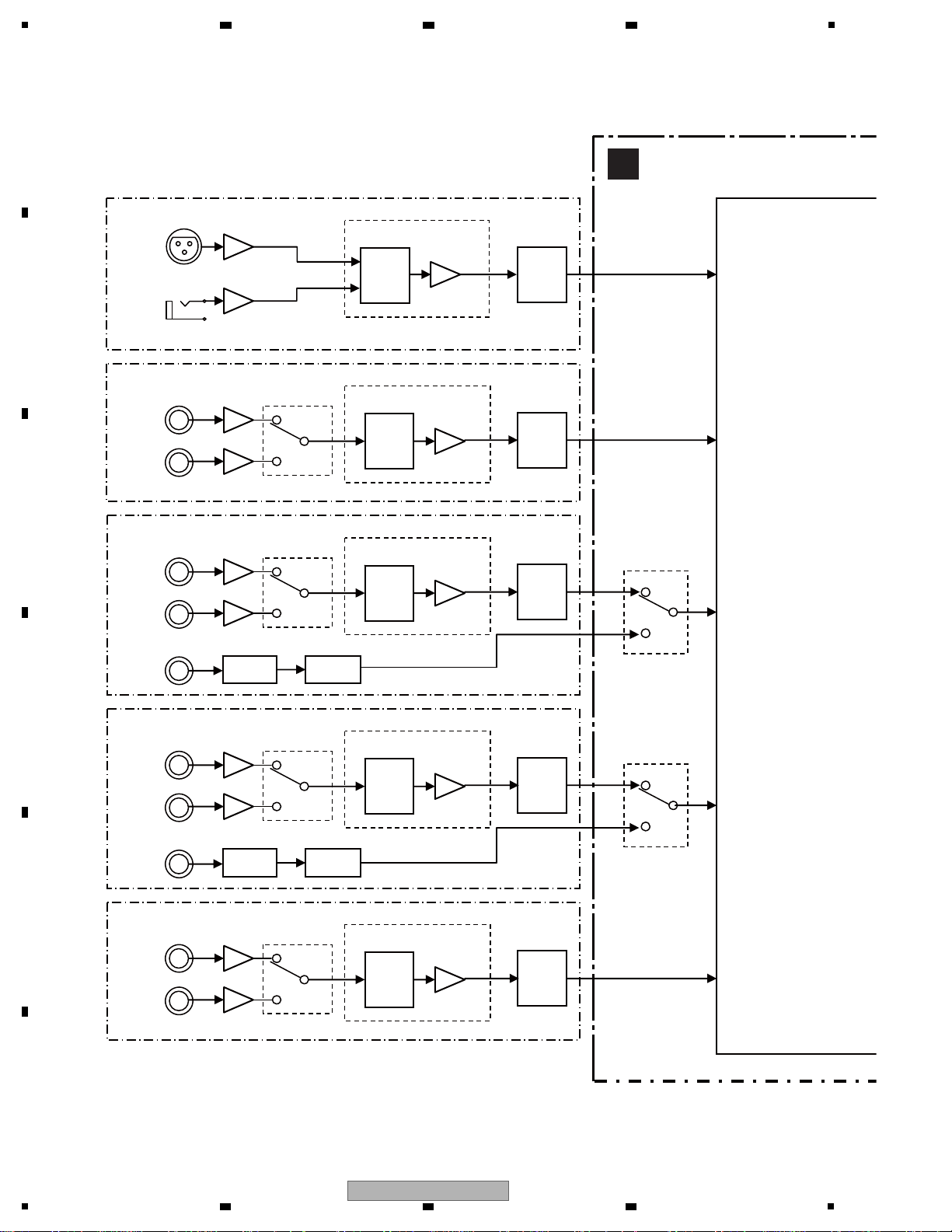
4. BLOCK DIAGRAM
4.1 OVERALL WIRING DIAGRAM
A
B
C
D
E
F
16
1
2 3 4
2 3 4
SVM-1000
Page 17
SW_MAT0
CH3
VIDEO SYNC
OUT
GND
19
14
14
7
22
G5
TOUCH PANEL
20
FFC
4P
4
3
OUT DDEN
29
HP_R
GLED
10
20
CH3_FADER
SW_SCAN4
19
2
V3R3REF1
8
3
23
6
20
17
DDD1385-
1mm FFC 24PIN
REVERSE
GREF1
1
19
CN9001
B2B-EH
GNDD
MUTE_OFF
V3R3
33
4L
3
MIL
SW_MAT5
21
RST_HP
R2
2
11
12
3VT
20
26
1
LED-10
V3R3REF1
2
INSEL1
SW_MAT0
V3R3REF2
19
GREF1
3AT
18
14
26
25
GNDD
1
10
2
17
V3R3REF1
V3R3
18
2
5
40
G4
TP1_XAD
BOTTOM
T_LEDD0A
22
31
2
T_LEDD0
GREF1
V3R3REF1
GNDD
B4
14
16
G2
CH4_FADER
SUB_CPU_INT
6
9
DKP3792-
PH
4PIN
9
5
28
EFF_CH_S0
8
LEDD12B
11
FIL_S1
TP1_XV
V3R3REF1
24
GNDD
6
35
DDD1389-
1.25mm FFC 28PIN
REVERSE
OUT DDT8
LEDD6A
TOP
2
30
1
4
GREF1
7
LEFT
16
V3R3REF1
CN7401
CKS4999-
31
ISNEL1
5
GNDHP
16
GREF1
2
20
23
SW_MAT6
CN3013
52492-2820
2
25
24
GNDHP
SW_SCAN3
GNDD
13
GREF1
TAP_SW
GREF2
SW_SCAN3
T_LEDD2
23
T_LEDD5
3
LED-0
FROM PDIV
14
2
14
6
TAP_SW
23
9
CH2_FADER
7
13
GREF1
11
1
2
37
2
GREF1
LED-6
V3R3REF1
CRS_FADER
18
10
17
18
35
10
SW_MAT4
26
LED-6
19
TOP PANEL
SW_SCAN3
_
2
4
5
V+15D
GNDD
LED-8
B1
22
PF05EE-D37
HP_DATA
10
17
23
SW_MAT2
10
13
T_LEDD0A
DDD1394-
1.25mm FFC
5PIN
REVERSE
1M
HP_DATA
SW_SCAN7
28
16
9
15
22
2
5
V3R3
2
22
GNDD
MAB
TIME_1
LED-4
22
21
LEDD9A
6
GNDD
CN6008
9610S-04B
26
CN1007
AKM1275-
B0
36
GNDD
LEDD14B
R4
TIME_1
BO
30
UP SIDE
TOUCH PANEL
G5
VLED(+5V)
5
2VT
13
12
34
6
25
8
SW7
GNDD
SW_MAT2
PWRFL(+15)
TP2_XV
34
GREF1
11
7
13
GNDD
5
GNDHP_L
5
12
GREF1
23
CLK
24
SMIC_TRIM
SW_MAT3
CN8751
S3B-PH-K-S
2
27
16
U/D
LEDD7B
8
19
CH3_FADER
B4
CN7101
52492-3620
1L
OUT DDT11
GNDD
LEDD7B
CH2_FADER
INSEL4
LEDD11B
FPGA_TX
1
14
LEDD3B
5
20
17
TIME_0
VLED(+5)
28
V3R3
G3
14
27
LEDD3B
19
HPL
23
7
17
LED-10
1
4 SW_MAT2
9
SW3
LCD_SW
CN7403
B4B-PH-K-S
15
10
INSEL4
5
LEDD5A
LED-7
18
OUT DDT15
29
SUB_CPU_BUSY
28
G0
OUT DDT3
GNDD
T_LEDD4
GNDD
19
8
15
10
2M
GLED
5
3
FIL_S1
SW1
28
HIGH VOLTAGE
V3R3
28
9
8
DCLK0
GNDD
3
LEDD11A
4
GND
13
16
OUT DDT9
6
LED0A
MUTE_OFF
EFFECT_ON
1012
GNDD
4
GND15
T_LEDD0A
GREF1
TP1_YAD
19
6
LEDD14B
GNDD
16
7
18
1
17
SW_MAT5
FL_PWR_H1
SW_SCAN3
6
8
HS
LEDD0B
37
CN8651
B4B-PH-K-S
B0
21
GNDD
FIL_S1
TP1_XV
3
INSEL2
20
DDD1390-
1.25mm FFC 36PIN
REVERSE
GNDHP_R
R5
SW_MAT5
SW_MAT5
8
36
V3R3REF1
SW4
14
MIC_TRIM
2
GNDD
16
1
20
G4
LEDD9B
27
28
GREF1
10
PHONES
1
GREF2
3
GNDD
GNDD
HP_L
GLED
GREF1
LEDD5B
3
23
GLED
1VT
10
LEDD6B
5
OUT DDEN
1
29
2L
OUT DDT10
9
INSEL2
GNDD
12
R0
GNDD
VLED(+5V)
SMIC_TRIM
LED-10
23
GNDD
18
CN6001
CKS3836-
GNDFL
GNDD
V3R3
GNDD
OUT DDT12
10
TP2_YV
SW2
3
23
16
OUT DDT4
1H
LEDD11B
1
VLED(+5V)
V3R3
11
33
3
4
2
4
13
5
8
13
2
21
CN3004
52147-0610
LED-2
6
19
CN6002
VKN1814-
16
24
2
12
13
6
LEDD14B
5
CN8452
52492-0620
HSYNC
V+15D
1
SW_SCAN4
12
1
LEDD9B
CH1_FADER
36
7
3
SW_MAT2
13
1
38
5
18
SW_MAT5
T_LEDD5A
14
2
V3R3REF2
25
1
21
22
36
SW7
12
LED-3
DCLKO
V3R3
8 GNDD
CN8951
52492-0520
SW5
DEPTH
GNDD
DIM_DUTY
24
1
GNDD
4
3
TP2_XAD
23
GNDD
(DSX1074)
HPM
GLED
18
OUT DDT13
11
SW_MAT0
SW2
LEDD1A
SW_SCAN4
GNDD
26
3
GNDFL
LEDD9B
14
22
40
22
23
V3R3
2
6
16
LEDD11A
GNDD
LEDD8B
14
35
4
CN3005
S8B-EH
LEDD8A
22
SW_MAT2
19
LEDD1B
GREF1
DIM_DUTY
SW_MAT0
SW4
LEDD13A
33
OUT DDT1
GNDD
TP1_YV
3
29
TP2_YV
4
LEDD6A
OUT DDT4
GNDD
30
V3R3
OUT DDT6
SW_MAT1
1
17
R1
4
GLED
LED-4
V3R3REF1
TP2_XV
21
GNDD
24
8
33
GNDD
GNDD
5
SW_MAT0
T_LEDD1A
29
DEPTH
GND
28
1
GNDD
6
EFFECT_ON
1
LEDD13B
CN7402
B2B-PH-K-S
20
CN3011
52492-3620
1
SW_MAT4
SW_MAT5
13
27
27
EFFECT_ON
GNDD
DKP3797PH
2PIN
SW_MAT0
CH4_FADER
36
SW_MAT3
4AT
1M
5
R1
SW3
V3R3REF1
G2
VSYNC
GLED
1
DDD1395-
0.5mm FFC 40PIN
12
3
4H
28
V3R3REF1
SW_MAT2
SW_SCAN4
LEDD2A
V3R3REF1
4H
3
CH3_FADER
7
GNDHP_R
SW6
27
V+3R3DREF
18
LEDD2B
LEDD8B
26
INSEL3
LEDD9A
CRS_FADER
15
EFFECT_ON
4M
TP1_XV
R0
2
OUT DDT12
7
11
GNDFL
33
GNDD
20
PF08EE-D30
OUT DDT14
GREF2
GNDD
GREF1
2
2
LCD_SW
VDD
TIME_0
GNDFL
FPGA_SCLK
T_LEDD1A
OUT DDT11
3
6
FIL_S1
9
V+5D
1
GND
4
9
4
FL_PWR_L1
_
GREF1
2
1
12
7
CN3006
DKN1480-
CN3007
52492-3620
SW_MAT0
3
28
T_LEDD2A
CH4_FADER
22
TP1_XAD
21
3
11
CH1_FADER
LED2A
6
3
CN8501
VKN1282-
7
1
R5
21
8
9
GREF1
6
40
2
OUT DDT3
B5
TIME_0
24
VDD
ERSE
VML
PF02EED32
CH1_FADER
15
12
T_LEDD4A
7
TAP_SW
LED-1
SW_MAT1
SW_MAT4
GNDD
PWRFL(+15)
TP1_XV
24
3H
11
8
GND
TIME_1
GNDD
14
23
EFF_CH_S0
29
GNDD
LEDD12B
LEDD4A
2
1
4
CH3_FADER
GNDD
23
SW_MAT2
GNDD
32
LEDD2A
8
LED-2
9
32
1AT
34
12
15
32
LED-8
6
1
11
10
PWRFL(+15)
3
LED-3
OUT DDT7
OUT DDT15
39
T_LEDD2A
5
4
LEDD12A
18
21
MAL
FL_PWR_L2
GNDFL
1004
21
5
18
CN3010
VKN1428-
DDD1392-
1.25mm FFC 36PIN
DDD1387-
1mm FFC
11PIN
GNDD
3
CN6005
52151-0610
LEDD3A
INSEL1
4
V3R3REF1
30
2
2H
28
3
19
1
GREF2
10
4
3H14
5
19
4
32
30
15
DE
LEDD5A
21
24
4
24
TP1_YAD
OUT DDT2
6
13
V3R3REF2
32
T_LEDD5A
13
TAP_SW
LED-1
3
8
FSYNC
24
SW_SCAN4
GLED
25
OUT DDT1
GND
5
6
LED3A
CN6007
CKS4428-
1
HERNESS
2PIN
SW_MAT5
GREF1
32
DDD1391-
1.25mm FFC 24PIN
18
1
B3
SW_MAT3
OUT DDT14
7
CH4_FADER
17
EFF_CH_S0
GND15
CH2_FADER
35
INSEL2
27
3
SW_SCAN7
3M
CRS_FADER
7
GNDD
LEDD0A
GNDD
ISNEL1
TP1_YAD
DDD1394-
1.25mm FFC
5PIN
REVERSE
R2
V3R3REF1
CH1_FADER
V3R3
12
GNDD
GNDD
INSEL3
V3R3
33
EFF_CH_S1
30
V3R3REF2
27
LED0A
13
16
LEDD7A
D+_USB2
7
31
LED-10
TOP
39
36
OUT DDT5
3L
DCLKO
23
3
4
21
21
GREF1
4
GLED
GNDD
G1
CN6804
52492-0520
5
15
CH1_FADER
VS
LEDD7A
TP2_YAD
FIL_S0
MAB
TIME_0
CN6003
VKN1814-
LOW VOLTAGE
9
3
35
CN6004
VKN1303-
1
22
18
GREF2
1VT
GREF1
3VT
T_LEDD15
SW_MAT3
OUT DDT9
U/D
2
GND
T_LEDD1
CN8401
52492-0620
17
CN7105
52492-0620
2
CN8601
AKM1290-
CN7402
S5B-EH
T_LEDD3A
5
OUT DDT8
5
5
SW_MAT4
21
VLED(+5)
15
13
GNDD
13
LEDD1A
20
6
LED-4
22
V3R3REF1
12
LEDD14A
LEFT
GNDD
LED0A
EFF_CH_S1
3
T_LEDD15A
GREF1
2
GREF1
12
9
GREF1
GNDD
GNDHP_L
VSYNC
5
VDD
T_LEDD5A
4
GNDD
11
SW_MAT0
DDD1394-
1.25mm FFC
5PIN
REVERSE
LED-3
MIH
17
LED1A
2
15
4
3
V+15D
LEDD14A
LED1A
GREF2
9
LED-3
1L
4
CN6801
52492-2820
MIC_TRIM
38
LEDD8A
8
LED-0
23
4
11
34
3
10
LEDD3A
22
FPGA_SCLK
VLED(+5V)
GNDFL
5
4L
17
3
EFF_CH_S0
17
34
7
6
EFFECT_ON
GNDD
1
21
GLED
26
20
GNDD
9
20
4
LED-10
4AT
15
B5
9
CN6006
CKS3192-
V3R3REF2
19
1
GNDD
27
FROM PDIV
13
SW_MAT5
31
GNDD
GNDD
CH4_FADER
3AT
1
TP1_XAD
7
VML
2
6
SW_MAT0
002
416-
33
LED-9
LEDD12A
24
GREF1
18
1
15
GREF1
LED-9
SW_SCAN4
LEDD10B
12
1
3M
22
3
SW_MAT2
TP2_XAD
27
L/R
6
GNDD
EFFECT_ON
GREF2
16
V3R3REF2
25
V-15A
VR_MUTE
4
11
17
SW_SCAN3
8
GNDD
11
PF02EE-
D32
20
24
RIGHT
SW032
2
4
34
17
4
17
GREF1
V3R3REF2
VSYNC
VLED(+5V)
V3R3REF1
LCD
4
GNDD
4
2
10
SW_MAT6
10
TP1_YV
11
1
3
20
B1
GNDD
4
HPL
21
19
TP1_YV
MIH
SW1
T_LEDD3
LED-3
14
11
8
37
GND
22
11
OUT DDT5
4
SW_MAT6
SW_MAT4
SW_MAT4
5
DEPTH
G3
16
SW_SCAN3
26
SW_MAT6
38
HP_L
V3R3REF1
LEDD4B
GNDD
6
2VT
G0
11
15
SW6
2
LEDD0A
19
INSEL3
OUT DDT6
LEDD4A
PWRFL(+15)
SW_SCAN4
4
GLED
2
GNDD
7
VLED(+5V)
2
SW_MAT1
GNDD
25
3
36
37
17
2
39
LEDD1B
OUT DDT10
1
2
3
1
FFC
4P
GREF1
3
TP1_YAD
29
1AT
EFF_CH_S1
6
25
VLED(+5V)
28
8
26
3
2AT
35
6
CN7103
52492-0520
22
CH4_FADER
10
26
CN3012
52492-2420
PWRFL(+15)
17
24
20
GNDD
9
2M
12
18
LEDD10A
2
GNDD
10
4VT
18
10
T_LEDD15A
LEDD5B
21
HPM
DDD1385-
1mm FFC 24PIN
REVERSE
3
19
LED-4
GNDD
36
8
8
TAP_SW
9
GNDD
V3R3REF1
30
2H
GNDD
15
CN3001
DKN1481-
HP_R
DOWN SIDE
TOUCH PANEL
V3R3REF1
11
7
GNDD
1
32
CN8451
CKS3825-
1
V+3R3DREF
GREF1
21
GNDD
6
CN6802
52492-3620
GNDD
PF03PP-D15
INSEL4
4
GNDD
10
CH3_FADER
8
MIC1
2
GNDD
TP2_YAD
12
LED1A
SW_MAT3
8
19
V3R3REF2
12
GND
HERNESS
2PIN
MIL
GREF1
FL_PWR_H2
19
4VT
25
CN8351
52492-0620
38
5
PWRFL(+15)
SW_MAT1
5
(CWX3405)
20
3
T_LEDD15A
4
SW_SCAN4
B2
LEDD14B
22
SW_MAT2
LEDD2B
LEDD4B
12
GNDD
GREF1
GNDD
D+_USB2
16
GNDFL
7
L/R
CN7104
52492-0520
GNDD
TP1_YV
SW_MAT3
GNDD
15
1
CN7102
52492-2420
INSEL2
15
34
DDD1393-
1.25mm FFC
6PIN
REVERSE
1
CH2_FADER
LED-7
SUB_CPU_RST
3
26
T_LEDD0A
DDD1393-
1.25mm FFC
6PIN
REVERSE
3
1
LEDD0B
_
FSYNC
5
7
15
CH2_FADER
B3
1
EFF_CH_S1
14
31
1
14
9
4
4
29
GNDD
SW_MAT0
2
9
5
4
2
GNDD
T_LEDD5A
16
CN3002
CKS5075-
3
11
16
GREF1
25
GREF1
OUT DDEN
15
7
33
10
CN9051
B2B-EH
30
CN3008
VKN1428-
13
VDD
35
CN8851
52492-0520
GNDD
FPGA_TX
23
DDD1386-
1mm FFC 22PIN
REVERSE
12
T_LEDD5A
GNDD
21
26
13
CH2_FADER
31
LEDD10B
GND
GNDD
CN6009
9610S-04B
GND15
FPGA_RX
19
GND
8
LED4A
TAP_SW
GREF1
CN9002
B2B-EH
LEDD13B
CRS_FADER
BOTTOM
11
4
14
CN3009
S3B-PH-K-S
10
GND
VR_MUTE
GLED
7
USB A
GREF2
17
DDD1394-
1.25mm FFC
5PIN
REVERSE
PWRFL(+15)
OUT DDT2
V3R3REF1
3
GNDD
27
9
SW_MAT5
2
14
29
G1
12
LEDD6B
GNDD
SW_MAT5
T_LEDD3A
16
PF04PPD05
2
4
GREF1
LEDD10B
22
RIGHT
11
15
20
FIL_S0
23
2
LEDD13A
FROM PDIV
11
30
FIL_S0
20
2
GLED
SW5
GNDD
14
JUMPER
6PIN
REVERSE
11
13
DEPTH
1
9
SW_MAT2
GNDFL
T_LEDD4A
4
OUT DDT7
3
GNDD
24
SUB_CPU_RST
1
9
4M
V+15A
SUB_CPU_INT
B2
GNDREF
9
LED-3
5
DDD1382-
1mm FFC 30PIN
OUT DDT13
INSEL3
LED-10
GLED
CH3_FADER
27
SW0
5
DDD1383-
1mm FFC 40PIN
T_LEDD0A
R4
OUT DDT0
3L
CN8901
52492-0520
BO
10
5
3
GNDA
16
4
24
18
GNDD
1
R3
24
PWRFL(+15)
31
24
LEDD9B
22
1H
RST_HP
31
MAL
GNDD
INSEL4
GREF1
5
VLED(+5V)
R3
17
T_LEDD0A
20
5
21
6
7
16
15
18
TIME_1
34
7
29
5
40
39
18
GNDREF
35
GNDD
GREF1
2AT
2L
FIL_S0
2
FPGA_RX
8
6
TP1_XAD
25
25
LEDD10A
OUT DDT0
1
30
10
12
CH1_FADER
LEDD10B
GNDA
CN8801
52492-0520
CN6803
52492-0520
D
HAMP ASSY
(DWX2726)
HJCK ASSY
(DWX2734)
MJCK ASSY
(DWX2738)
Z
H H( 1/2- 2/2)
H
SCPU ASSY
(DWX2716)
ILMR ASSY
(DWX2722)
AF
ILML ASSY
(DWX2723)
AG
L
CFD1 ASSY
(DWX2740)
M
CFD2 ASSY
(DWX2741)
N
CFD3 ASSY
(DWX2742)
O
CFD4 ASSY
(DWX2743)
K
CTL2B ASSY
(DWX2736)
I
CTL1 ASSY
(DWX2729)
J
CTL2A ASSY
(DWX2735)
T
CRFD ASSY
(DWX2739)
P
INVT ASSY
(DWX2717)
R
CTL3LB ASSY
(DWX2745)
Q
CTL3R ASSY
(DWX2730)
S
CTL3LA ASSY
(DWX2744)
Therefore, when replacing, be sure to use parts of identical designation.
When ordering service parts, be sure to refer to "EXPLODED VIEWS and PARTS LIST" or "PCB PARTS LIST".
The > mark found on some component parts indicates the importance of the safety factor of the part.
: The power supply is shown with the marked box.
5
6 7 8
5
SVM-1000
6 7 8
A
B
C
D
E
F
17
Page 18
1
MIC1, 2
CH1
MIC
D-TRIM
IC4001
IC4003
IC4004
IC4009
MIC1
IC4001
147
MIC2
CH1
D-TRIM
IC4017
DVD
IC4012
IC4011
IC4020
IC4021
RY4001
IC4032
IC1083
IC4026
IC4035
IC4036
RY4002
IC5032
IC5041
IC5042
RY5003
IC5047
IC5056
IC5057
RY5004
PHONO
143
CH2
D-TRIM
DVD
IC4027
IC6503 IC6505
IC6504 IC6506
LINE
CH2
144
DIGITAL
CH3
D-TRIM
IC5038
DVD
IC1084
IC5033
LINE
CH3
145
DIGITAL
CH4
D-TRIM
CH4IC5048
PHONO
146
IC5053
DVD
DSP
IC1001
DIR
SRC
A/D
A/D
A/D
DIR SRC
A/D
A/D
MAIN ASSY
G
4.2 AUDIO BLOCK DIAGRAM
A
2 3 4
B
C
D
E
F
18
1
SVM-1000
2 3 4
Page 19
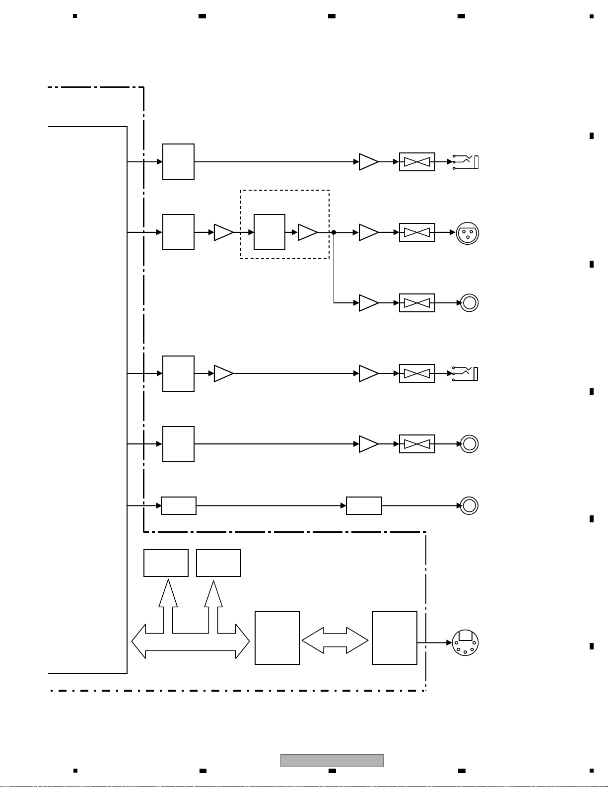
5
MUTE
HP HP
13
D-TRIM
MUTE
MASTER MASTER1
27
IC5021
MUTE
MASTER2
BOOTH BOOTH
20
MUTE
MUTE
REC REC
18
D-OUT
DIGITAL OUT
17
IC1003
IC6517 IC6516
IC5020
IC5019
IC4044
IC5004
IC7404
IC7406
L: IC4045
R: IC4046
L: IC5008
R: IC5009
L: IC5011
R: IC5010
L: IC5013
R: IC5012
L: IC5015
R: IC5014
L: IC4048
R: IC4047
IC1101
IC1055 IC1070
MIDI OUT
ADSP BUS
D/A
D/A
D/A
D/A
SRC DIT
SDRAM
FLASH
ROM
FPGA1
CPU BUS
UCOM
6 7 8
A
B
C
D
5
6 7 8
SVM-1000
E
F
19
Page 20
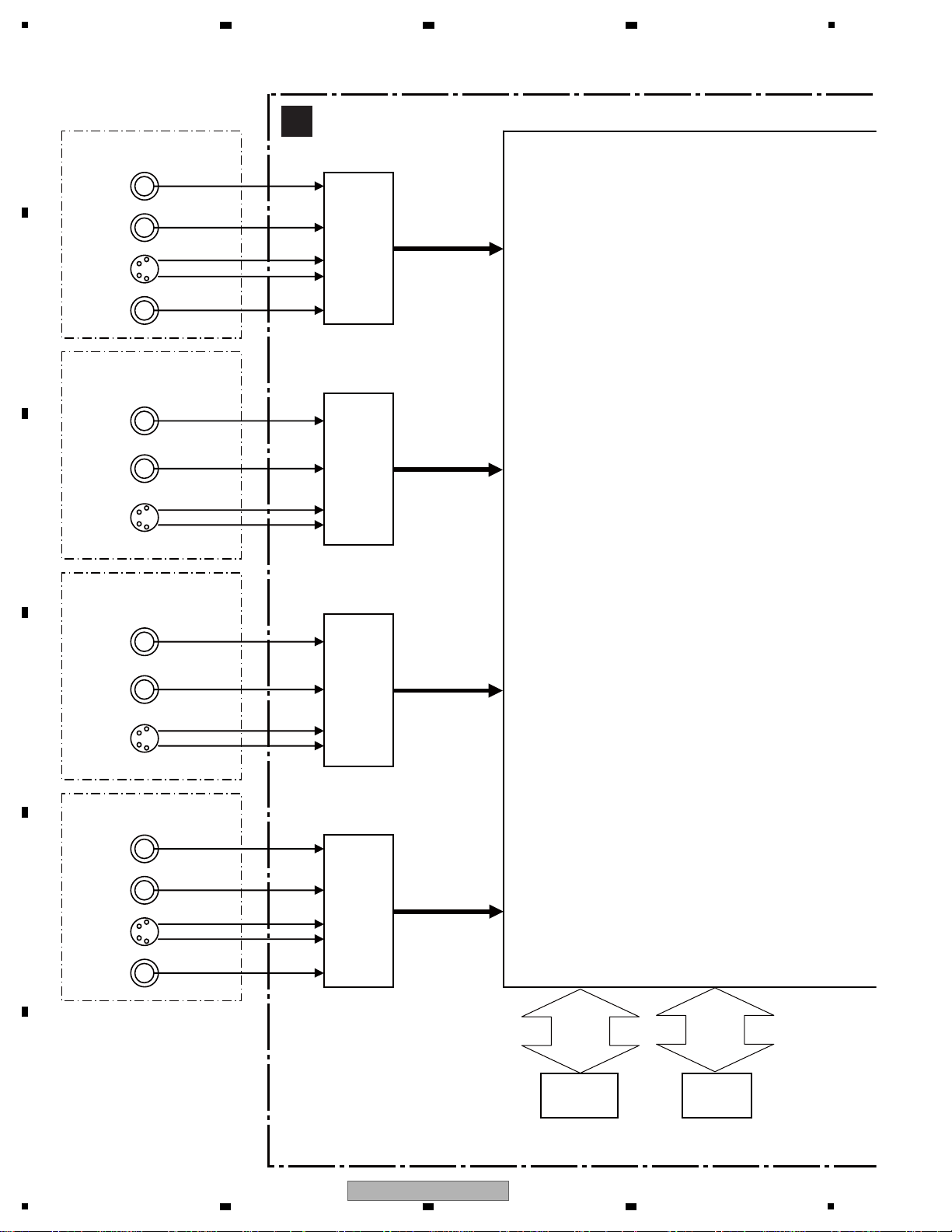
1
MAIN ASSY
G
CH1
IC1048
S-VIDEO
46
49
VIDEO
DATA
DVD
48
VIDEO
35
CH2
VIDEO EX
36
IC1049
DVD
36
VIDEO
48
OEDIV
DATA
S-VIDEO
46
49
CH3
IC1052
DVD
36
DATA
S-VIDEO
46
49
VIDEO
48
VIDEO
CH4
IC1053
DVD
48
VIDEO
35
S-VIDEO
46
49
VIDEO
DATA
VIDEO EX
36
IC1062 IC1057
ADC
ADC
ADC
ADC
FPGA2
IC1058
SDRAM
DDR
SDRAM
FPGA2_
DDR
BUS
FPGA2_
SDRAM
BUS
4.3 VIDEO BLOCK DIAGRAM
A
B
2 3 4
C
D
E
F
20
SVM-1000
1
2 3 4
Page 21
IC1035
IC1041
MASTER COMPOSITE (RCA)
IC1038
MASTER COMPOSITE (BNC)
2
6
MASTER S-VIDEO
8
Y
MASTER COMPONENT
16
IC1040
IC1039
MONITOR COMPOSITE (RCA)
2
6
MONITOR S-VIDEO
8
IC1043
IC1044 to IC1047
IC1070
IC1100
IC1036
IC1066
IC1008
IC1009,IC1010
LCD DATA
DAC
VIDEO
AMP
DAC
VIDEO
AMP
SD SLOT
USB
USB MIDI
HOST BUS
SD IC
USB IC
VIDEO
DSP
SDRAM×4
FPGA2_
VDSP
BUS
VDSP_
SDRAM
BUS
LCD
GDC
SDRAM×2
GDC_SDRAM
UCOM
CPU BUS
HOST
HOST
FLASH
SDRAM
CPU BUS
CPU BUS
CPU BUS
11
14
VIDEO
DATA
VIDEO
DATA
CB
CR
5
6 7 8
A
B
C
D
5
6 7 8
SVM-1000
E
F
21
Page 22
1
MAIN ASSY
G
CRFD ASSY
T
CTL1 ASSY
I
SCPU ASSY
H
CTL3LB ASSY
R
DIO1 ASSY
V
AUD2 ASSY
B
CTL3LA ASSY
S
122
UCOM
IC1070
SUB CPU
IC3010
FPGA2
IC1058
Communication Line
CTL1 SW, SELECTOR
CH1, 2 FADER
CTL1 LED
LED MAT
SW MAT
CTL1 VOLUME
VR IN
LED MAT
SW MAT
CNT3LB SW CNT3LB LED
CNT3LA LEDCNT3LA SW
LED MAT
SW MAT
CROSS FADER
SAMPLING F
SELECTOR
ATT
CPU
BUS
90, 91
94 97
84, 85, 86
2 3 4
4.4 FUNCTION BLOCK DIAGRAM
A
B
C
D
E
F
22
1
2 3 4
SVM-1000
Page 23
5
CTL2A ASSY
J
CTL2B ASSY
K
CTL3R
ASSY
Q
124
92, 93
170
EFFECT ON/OFF TAP
CTL3R VOLUME
EFFECT CUE
LED MAT
SW MAT
VOLUME
CTL2A SW, SELECTOR
CH3, 4 FADER
CTL2A LED
LED MAT
SW MAT
CTL2A VOLUME
VR IN
LED MAT
Communication Line
SW MAT
TOUCH
PANEL
CROSS FADER
CURVE
SD LAMP
48, 49, 52, 53
82, 29
80, 87,
95, 96
138, 171
6 7 8
A
B
C
D
5
6 7 8
SVM-1000
E
F
23
Page 24
1
Start of diagnosis
Start up Service mode.
Does the LCD display appear?
Perform diagnosis procedures for each device
indicated on the DEVICE CHECK screen.
GDC NG Sub CPU NG
Yes
Yes
No
No
Is the VIDEO SOLO MODE LED
lit?
To enter Service mode, turn on the unit by
pressing the CH4 FADER START, CH2 CUE,
and FADER AV SYNC buttons simultaneously.
To change pages, press the
EFFECT ON/OFF button.
Diagnosis Flowchart
5. DIAGNOSIS
5.1 DIAGNOSIS FLOW
A
2 3 4
B
C
D
E
F
24
1
2 3 4
SVM-1000
Page 25
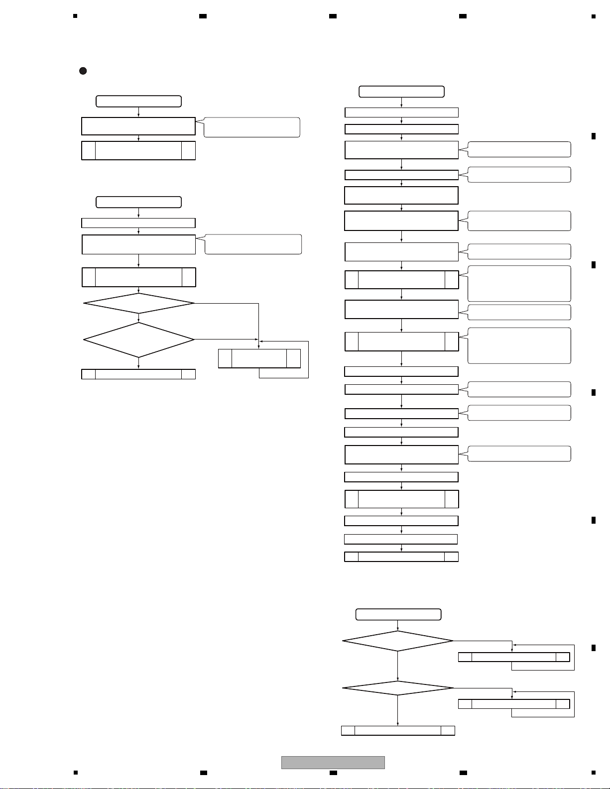
5
5.2 POWER ON SEQUENCE
6 7 8
Main Microcomputer
Power ON.
Resetting of the Main micro-
computer is canceled.
The booting section
starts up.
Booting section
Each device is reset.
Resetting of the Submicro-
computer/GDC is canceled.
The program section is
developed in SDRAM.
Download mode?
No
The compatibility
of the program is
checked.
GOOD
The program starts up.
Yes
NG
Resetting is canceled when
Pin 37 is set to High.
Resetting is canceled when
Pin 83 is set to HIGH.
Process of
Download mode
Program section
Drawing data are transmitted to GDC.
Startup screen 1 is displayed.
A request for start of communication
with the submicrocomputer is issued.
Resetting of VADC/VDAC is canceled.
Waiting for start of communication
with the submicrocomputer.
Communication with the sub-
microcomputer starts.
A request to clear the FPGA1
program is issued.
Loading of the FPGA1
program starts.
A request to clear the FPGA2
program is issued.
Loading of the FPGA2
program starts.
Waiting for startup of FPGA
Resetting of AudioDSP is canceled.
With Pin 171 set to HIGH
With Pin 51 set to HIGH
Waiting time: 10 msec
Start of switching Pin 171 between
H and L triggers communication.
With Pin 74 set to HIGH
The FPGA1 program is cleared with
Pin 69 set to H, data are output
with Pin 81 set to H, and a clock is
output with Pin 50 set to H.
With Pin 70 set to HIGH
The FPGA2 program is cleared with
Pin 53 set to H, data are output
with Pin 81 set to H, and a clock is
output with Pin 50 set to H.
Waiting time: 7 msec
With Pin 86 set to HIGH
A
B
C
Resetting of VideoDSP is canceled.
Waiting for Video DSP stabilization
Resetting of FPGA1 and FPGA2
is canceled.
Waiting for canceling of FPGA reset
Loading of the Video DSP
program
Real-time initialization of the OS
Creation of each task
Real-time startup of the OS
Main task section
Checker mode?
No
Service mode?
No
With Pin 121 set to HIGH
Waiting time: 7 msec
With Pin 61 set to HIGH
Waiting time: 1 msec
Yes
Process of Checker mode
Yes
Process of Service mode
D
E
F
Main process
SVM-1000
5
6 7 8
25
Page 26
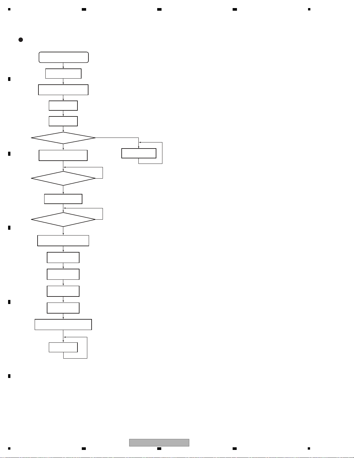
1
AV mixer submicrocomputer
A
Canceling of resetting of
the submicrocomputer
Interrupt mask
Setting of microcomputer
operations
Port setting
2 3 4
B
C
D
Timer setting
Flashing OK?
Yes
The LEDs for TAP and
EFFECT ON/OFF light.
Does the LCD start
normally?
The LCD starts up.
Does the system start
normally?
The LEDs for TAP and
EFFECT ON/OFF go dark.
Setting of AD
converter
Setting of serial
communications
Yes
Yes
*1
No
Error processing
*4
No
*1 LCD's startup is OK with Pin 29 set to H.
(Signal name: SUB_CPU_BUSY)
*2 Set Pin 41 to H. (Signal name: LCD_SW)
*3 Startup of the system is OK with Pin 29 set to L.
*2
(Signal name: SUB_CPU_BUSY)
*4 Waiting for the command for start of downloading from the main microcomputer
(During waiting, the FADER START CH1 to CH4 LEDs cyclically light then go
No
*3
dark.)
Initialization of
global works
Canceling of
interrupt mask
Initialization of the LEDs and
keys, start of the main timer
E
Main process
F
26
1
2 3 4
SVM-1000
Page 27
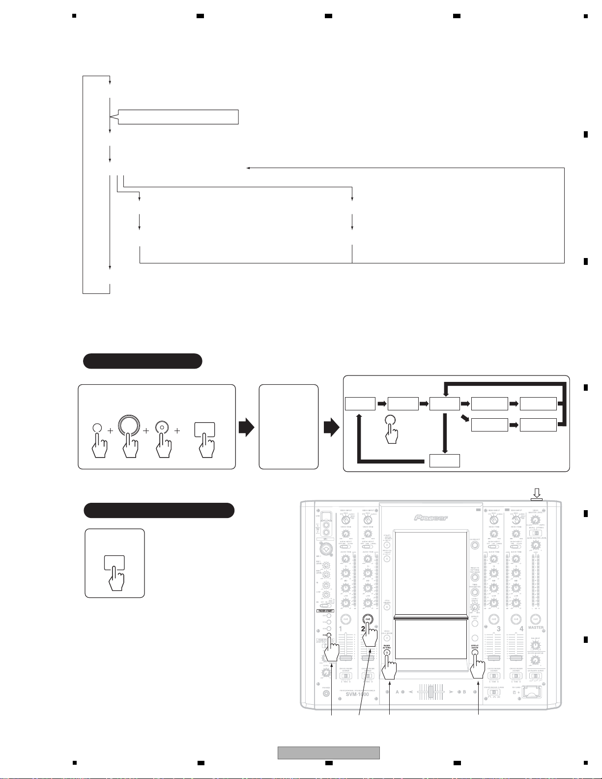
5
Page 0 VERSION
Mode to display the versions of the main CPU, sub CPU, Audio DSP, video DSP, FPGA1, and FPGA2
Page 1 Device Check
Mode to check whether the devices are operating
Page 2 Calibration
Touch-Panel Calibration Mode
Page 2-1 Top Panel Calibration
Calibration for the top panel
Page 2-2 Top Panel Check
Calibration check mode for the top panel
Page 3 System Setting
PAL/NTSC setting mode
Page 2-3 Bottom Panel Calibration
Calibration for the bottom panel
Page 2-4 Bottom Panel Check
Calibration check mode for the bottom panel
Press the EFFECT ON/OFF key.
CUE
CH4
POWER
CH-2
Page 1
POWER ON
(Rear panel)
POWER OFF
(Rear panel)
Page 0 Page 2 Page 2-1 Page 2-2
Page 2-3
Page 2-4
Page 3
(Cyclic operations)
Service Mode : ON
Service Mode : CANCEL
FADER
AV SYNC
FADER
AV SYNC
FADER
STAR T
CH2
CUE
EFFECT
ON/OFF
EFFECT
ON/OFF
LCD
TOP PANEL
LCD
BOTTOM PANEL
Service Mode
(Page 0 is
displayed on the
LCD display.)
6 7 8
6. SERVICE MODE
6.1 LIST OF PAGES IN SERVICE MODE
A
B
6.2 SERVICE MODE
C
D
E
5
SVM-1000
6 7 8
F
27
Page 28
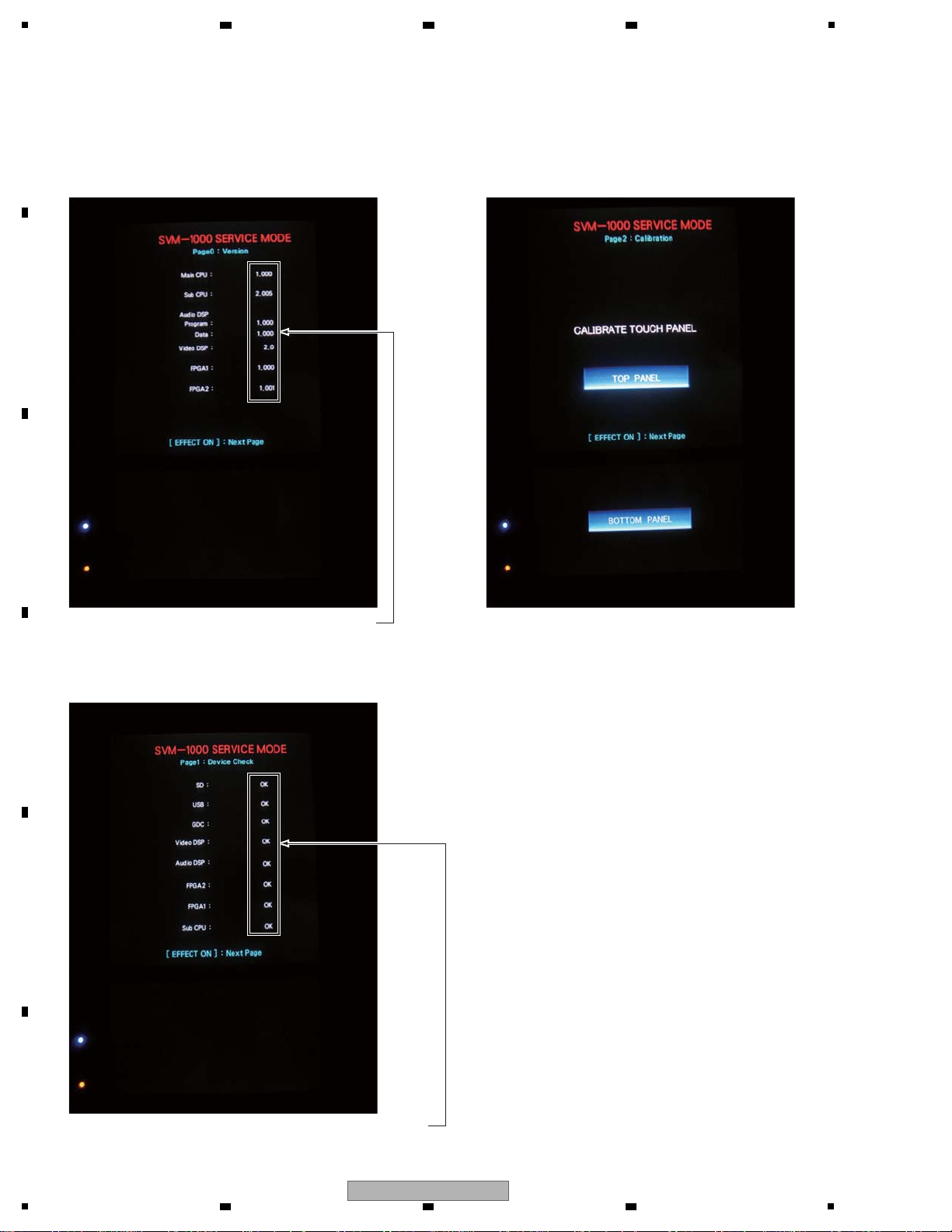
1
2 3 4
6.3 SERVICE MODE IDENTIFICATION
A
Page0 : VERSION
Mode to display the versions of the main CPU, sub CPU,
Audio DSP, video DSP, FPGA1, and FPGA2
B
C
Page2 : Calibration
Touch-Panel Calibration Mode
The versions of the respective devices are displayed.
The version of the main CPU is also used as the
product version.
Page1 : Device Check
Mode to check whether the devices are operating.
D
E
TOP PANEL
Perform calibration for the top panel (page 2-1).
BOTTOM PANEL
Perform calibration for the bottom panel (page 2-3).
F
Any defective blocks of the product can be detected in this mode.
If the corresponding device has been activated normally, “OK” is displayed.
For a device detected to be abnormal, “NG” is displayed.
28
1
2 3 4
SVM-1000
Page 29
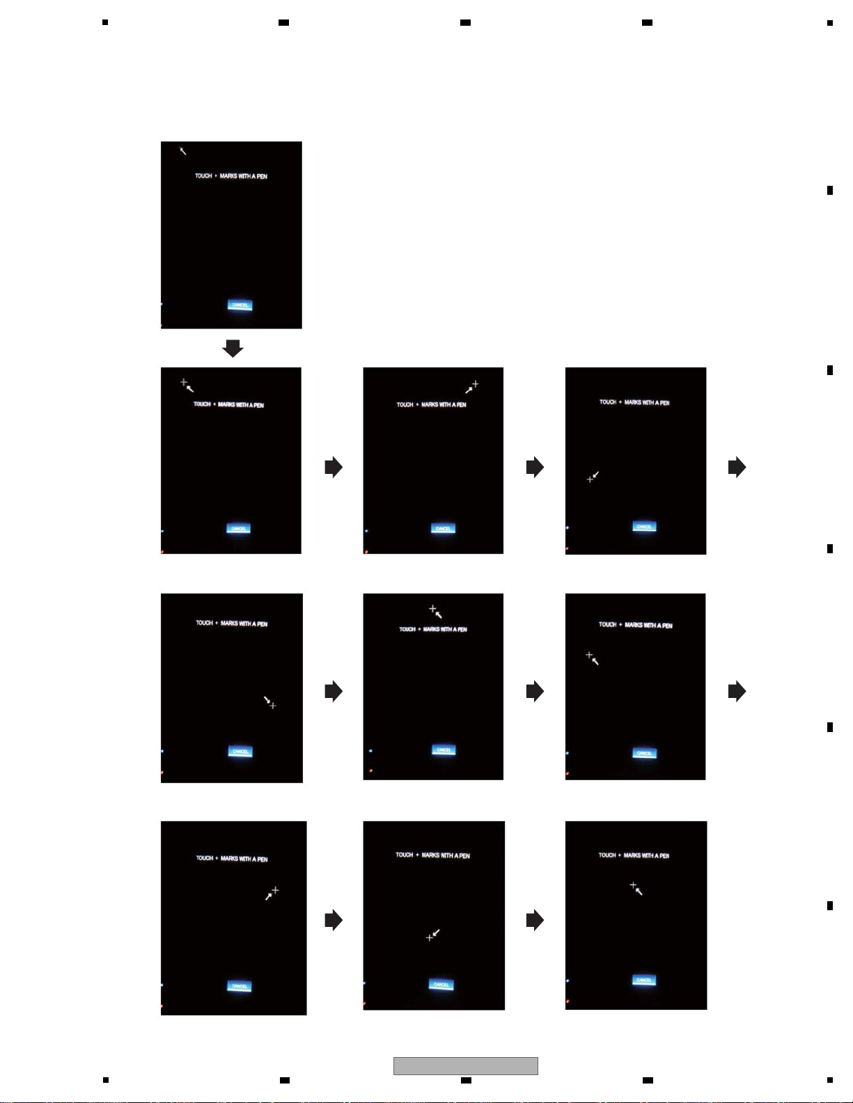
5
6 7 8
Page2-1 : Top Panel Calibration
Calibration for the top panel
A
Perform calibration on point 1 and the subsequent 9 points on the touch panel.
A + symbol is displayed at each point in sequence.
Touch the center of the + symbol with a pointed tool, such as a stylus pen.
When you finish touching all the points, the display changes to Page 2-2.
B
C
D
E
F
SVM-1000
5
6 7 8
29
Page 30
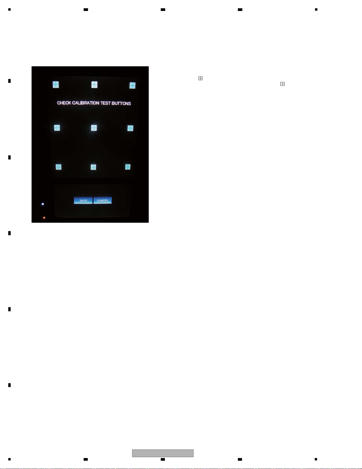
1
Page2-2 : Top Panel Check
A
Calibration check mode for the top panel
B
2 3 4
Check the result of the calibration.
Touch the center of with a pointed tool, such as a stylus pen.
When the calibration has finished successfully, the color of changes
from blue to white.
SAVE: To store the calibration settings of the top panel.
CANCEL: To cancel the calibration settings of the top panel.
C
D
E
F
30
1
2 3 4
SVM-1000
Page 31

5
6 7 8
Page2-3 : Bottom Panel Calibration
Calibration for the bottom panel
Perform calibration at point 1 and the subsequent 6 points on the touch panel.
A + symbol is displayed on each point in sequence.
Touch the center of the + symbol with a pointed tool, such as a stylus pen.
When you finish touching all the points, the display changes to Page 2-4.
A
B
C
D
E
F
SVM-1000
5
6 7 8
31
Page 32

1
Page2-4 : Bottom Panel Check
A
Calibration check mode for the bottom panel
B
2 3 4
Check the result of the calibration.
Touch the center of with a pointed tool, such as a stylus pen.
When the calibration has finished successfully, the color of changes
from blue to white.
SAVE: To store the calibration settings of the bottom panel.
CANCEL: To cancel the calibration settings of the bottom panel.
C
Page3 : System Setting
PAL/NTSC setting mode
D
E
Perform the factory presetting of the video system.
Set it to the corresponding system for the destination area.
Move the cursor with the k (left) or l (right) key to the desired setting
then press the SAVE button.
PAL
To set the video system to PAL.
NTSC (7.5IRE)
To set the video system to NTSC (7.5IRE).
NTSC (0IRE)
To set the video system to NTSC (0IRE).
The settings for each destination are shown below:
Destination
North America
Europe
Japan
China
General
/KUCXJ
/WYXJ5
/JJXJ
/WAXJ5
/TLXJ
Video Format
NTSC (7.5IRE)
PAL
NTSC (0IRE)
PAL
NTSC (0IRE)
F
32
1
2 3 4
SVM-1000
Page 33

5
6 7 8
6.4 LIST OF PAGES IN TEST MODO
Page 0 Main Page / VERSION
Mode to display the versions of the main CPU, sub-CPU, Audio DSP, video DSP, FPGA1, and FPGA2
A
Press the EFFECT ON/OFF key.
Key/VR Check Mode
: Press the EFFECT ON/OFF key.
: Press the TAP key.
Page 1 LED ALL ON
Mode to light all LED and FL segments
Page 2 LED ALL OFF
Mode to turn all LED and FL segments off
Page 3 KEY TEST
Mode to indicate the pressed key
Page 4 SWITCH TEST
Mode to indicate the switch positions
Page 5-1 VOLUME TEST (1)
Mode to indicate the volume-control positions
Page 5-2 VOLUME TEST (2)
Mode to indicate the volume-control positions
Page 6 METER TEST
Mode to check the LED segments of the meters by turning them on one by one
Each time you press the CUE key, the LED segments of the meters for each channel light one
by one. All segments are dark at the beginning. When you press the key again after your 15th
press of the key (when the top LED is lit), all segments will go dark again, permitting the test to
be repeated from the beginning.
Press the EFFECT ON/OFF key to return to the main page.
B
C
Press the TAP key.
LCD/Touch Check Mode
Page 7 TOUCH PANEL TEST
Mode to indicate the coordinates on the touch panels being touched
Page 8-1 MAIN PANEL TEST
For checking the display colors on the main panel (color bars)
Page 8-2 SUB PANEL TEST
For checking the display colors on the sub-panel (color bars)
Page 9-1 MAIN PANEL TEST
For checking for defective dots on the main panel (white)
Page 9-2 SUB PANEL TEST
For checking for defective dots on the sub-panel (white)
Page 10-1 MAIN PANEL TEST
For checking the luminescent spots on the main panel (black)
Page 10-2 SUB PANEL TEST
For checking the luminescent spots on the sub-panel (black)
Press the EFFECT ON/OFF key to return to the main page.
D
E
F
SVM-1000
5
6 7 8
33
Page 34

1
CUE
CH2
POWER
CH-1
POWER ON
(Rear panel)
POWER OFF
(Rear panel)
Page 0
Test Mode
(Page 0 is displayed
on the LCD display.)
(Cyclic operations)
Test Mode : ON
Test mode : CANCEL
FADER
AV SYNC
FADER
AV SYNC
FADER
STAR T
FADER
START
CH2
CH1
CUE
EFFECT
ON/OFF
TAP
EFFECT
ON/OFF
(Cyclic operations)
EFFECT
ON/OFF
EFFECT
ON/OFF
LCD
TOP PANEL
LCD
BOTTOM PANEL
TAP
Page 1 Page 2 Page 3
Page 4
Page 5-1Page 5-2Page 6
Page 8-2 Page 8-1 Page 7
Page 9-1
Page 10-2Page 10-1Page 9-2
Key/VR Check ModeLCD/Touch Check Mode
6.5 TEST MODE
A
2 3 4
B
C
D
E
F
34
SVM-1000
1
2 3 4
Page 35

5
6 7 8
6.6 TEST MODE IDENTIFICATION
A
Page0 : Main Page / VERSION
Mode to display the versions of the main CPU, sub-CPU,
Audio DSP, video DSP, FPGA1, and FPGA2
In the figure below, the version of the main CPU is 1.100.
Page2 : LED ALL OFF
Mode to turn all LED and FL segments off
Check that all the segments are dark.
Page3 : KEY TEST
Mode to indicate the pressed key
B
C
The versions of the respective devices are displayed.
Press the EFFECT ON/OFF key to shift to Key/VR
Check mode.
Press the TAP key to shift to LCD/Touch Check mode.
Page1 : LED ALL ON
Mode to light all LED and FL segments
Check that all the segments are lit.
D
E
When you press a key, the corresponding indication
changes to “ON” (lit in red).
While the key is not pressed, the indication is “OFF”
(lit in white).
F
SVM-1000
5
6 7 8
35
Page 36

1
2 3 4
Page4 : SWITCH TEST
Mode to indicate the switch positions
Check that the settings are switched properly.
A
B
C
When you change a switch setting, the corresponding
indication of the selected position lights in red.
Page5-2 : VOLUME TEST (2)
Mode to indicate the volume-control positions
Check that the volume controls (CH3/CH4/FADER
/MASTER/BOOTH blocks) function properly.
The A/D-converted values of the volume
control settings are displayed as bars.
Page5-1 : VOLUME TEST (1)
Mode to indicate the volume-control positions
Check that the volume controls (MIC/HEADPHONE/CH1
/CH2 blocks) function properly
The A/D-converted values of the volume
D
E
control settings are displayed as bars.
The A/D-converted values of the volume control settings
are numerically displayed in the range from 0 to 1023.
The A/D-converted values of the volume control settings
F
36
are numerically displayed in the range from 0 to 1023.
1
2 3 4
SVM-1000
Page 37

5
6 7 8
Page6 : METER TEST
Mode to check the LED segments of the meters by turning them on one by one
Each time you press the CUE key, the LED segments of the meters for
each channel light one by one.
All segments are dark at the beginning. When you press the key again
after your 15th press of the key (when the top LED is lit), all segments
will go dark again, permitting the test to be repeated from the beginning.
CH1 CUE : CH1 level meter
CH2 CUE : CH2 level meter
CH3 CUE : CH3 level meter
CH4 CUE : CH4 level meter
MASTER CUE : MASTR L CH level meter
EFFECT CUE : MASTR R CH level meter
A
B
Page7 : TOUCH PANEL TEST
Mode to indicate the coordinates on the touch panels being touched
Check the responses of the touch panels.
Press the touch-panel check buttons. Proper responses of the buttons
mean that the touch panels function properly.
If there is any misalignment, activate Service mode to re-calibrate the
panels.
While you are touching the lower (bottom) touch panel,
the corresponding coordinates on the panel are displayed.
Touch-panel check buttons
When you touch them correctly, the color of each touched
button changes between blue and red.
CH1
CUE
CH2
CUE
EFFECT
CUE
CH3
CUE
CH4
CUE
MASTER
CUE
C
D
E
While you are touching the upper (top) touch panel,
the corresponding coordinates on the panel are displayed.
F
SVM-1000
5
6 7 8
37
Page 38

1
2 3 4
Page8-1 : MAIN PANEL TEST
For checking the display colors on the main panel
(color bars)
A
Check the LCD display of the main panel.
Confirm that the colors are displayed properly.
B
C
Page8-2 : SUB PANEL TEST
For checking the display colors on the sub-panel
(color bars)
Check the LCD display of the sub-panel.
Confirm that the colors are displayed properly.
D
E
F
38
SVM-1000
1
2 3 4
Page 39

5
6 7 8
Page9-1 : MAIN PANEL TEST
For checking for defective dots on the main panel (white)
Check the LCD display of the main panel.
Confirm that there are no defective dots (no dots that do
not become white).
Page9-2 : SUB PANEL TEST
For checking for defective dots on the sub-panel (white)
Check the LCD display of the sub-panel.
Confirm that there are no defective dots (no dots that do
not become white).
A
B
C
D
E
F
SVM-1000
5
6 7 8
39
Page 40

1
2 3 4
Page10-1 : MAIN PANEL TEST
For checking the luminescent spots on the main panel
A
(black)
Check the LCD of the main panel.
Confirm that there is no colored block remaining.
B
C
Page10-2 : SUB PANEL TEST
For checking the luminescent spots on the sub-panel
(black)
Check the LCD of the sub-panel.
Confirm that there is no colored block remaining.
D
E
F
40
SVM-1000
1
2 3 4
Page 41

5
6 7 8
6.7 HOW TO USB DOWNLOAD
Necessary items
SVM-1000
USB flash memory
Firmware file (AVMxxxx.upd)
Procedures
1 Place the firmware file in the root directory of the USB
flash memory.
Note: Do not place any files in this folder other than ones
with the .upd extension.
3 Hold the POWER key pressed for 5 seconds while
holding the EFFECT ON/OFF and TAP keys pressed.
POWER
VIDEO INPUT
USB
CH 1
VIDEO
EX
CH 4
MIC 1
MIC1
LEVEL
MIC2
LEVEL
HI
LOW
MIC OFF ON
FADER START
HEAD PHONES
MONOSPLIT STEREO
CUE
MIC
0
0
+12-12
+12-12
TALK
OVER
CH1
CH2
CH3
CH4
MIXING
MASTER
LEVEL
0
PHONES
VIDEO INPUT
VIDEO INPUT
VIDEO
DVD
DVD
S-VIDEO
VIDEO
EX
VIDEO TRIM
VIDEO TRIM
MIN
MAX
MIN
AUDIO INPUT
AUDIO INPUT
DVD/LINE PHONO
DVDLINE DIGITAL
AUDIO TRIM
AUDIO TRIM
OVER
10
+9
7
HI
4
2
1
0
+6-26
–1
MID
–2
–3
–5
+6-26
–7
LOW
–10
–15
–24
+6-26
dB
CUE
1
2
10
9
8
7
6
5
4
3
2
1
0
CROSS FADER
CROSS FADER
ASSIGN
ASSIGN
A THRU B
A THRU B
PROFESSIONAL SOUND&VISION MIXER
SVM-1000
BA
PARAMETER
CH SELECT
VIDEO FX
PATTERN/
TEXT BANK
TIME/
LEVEL/
DEPTH
MAXMIN
EFFECT
CUE
EFFECT
ON/OFF
VIDEO INPUT
VIDEO
DVD
VIDEO TRIM
MIN
AUDIO INPUT
DVDLINE DIGITAL
AUDIO TRIM
OVER
10
7
HI
4
2
1
0
–1
MID
–2
–3
–5
–7
LOW
–10
–15
–24
dB
CUE
10
9
8
7
6
5
4
3
2
1
0
CROSS FADER
ASSIGN
A THRU B
CROSS FADER CURVE SD CARD
VIDEO
S-VIDEO
UTILITY
MASTER
MAX
MONITOR
SET UP
VIDEO EQ
OVER
ON/OFF
SET UP
10
+9
7
HI
4
2
1
0
+6-26
–1
MID
–2
–3
–5
+6-26
–7
LOW
–10
JPEG
–15
VIEWER
–24
+6-26
dB
CUE
VIDEO
SOLO MODE
10
9
8
7
6
FADER
5
AV SYNC
4
3
2
1
0
EFFECT
S-VIDEO
MAX
+9
+6-26
+6-26
+6-26
3
TAP
VIDEO
MASTER LEVEL
VIDEO
DVD
S-VIDEO
VIDEO
EX
WHITEBLACK
VIDEO TRIM
MONO STEREO
AUDIO MASTER LEVEL
MIN
MAX
AUDIO INPUT
LINE PHONO
0
AUDIO TRIM
OVER
OVER
10
10
+9
7
7
HI
4
4
2
2
1
1
0
0
+6-26
–1
–1
MID
–2
–2
–3
–3
–5
–5
+6-26
–7
–7
LOW
–10
–10
–15
–15
–24
–24
+6-26
dB
dBLR
CUE
CUE
MASTER
4
10
9
BALANCE
8
7
6
5
4
RL
3
BOOTH MONITOR
2
1
0
0
CROSS FADER
ASSIGN
CH FADER CURVE
A THRU B
ON/OFF
4 "Download Information" will be displayed on the LCD
display shortly.
A
B
C
2 Plug the USB memory device into the USB slot located
on the upper panel.
VIDEO INPUT
USB
USB
CH 1
VIDEO
EX
CH 4
MIC 1
MIC1
LEVEL
MIC2
LEVEL
HI
LOW
MIC OFF ON
FADER START
HEAD PHONES
MONOSPLIT STEREO
CUE
MIC
0
0
+12-12
+12-12
TALK
OVER
CH1
CH2
CH3
CH4
MIXING
MASTER
LEVEL
0
PHONES
VIDEO INPUT
VIDEO
DVD
S-VIDEO
VIDEO
EX
VIDEO TRIM
MIN
MAX
MIN
AUDIO INPUT
DVD/LINE PHONO
DVDLINEDIGITAL
AUDIO TRIM
OVER
10
+9
7
HI
4
2
1
0
+6-26
–1
MID
–2
–3
–5
+6-26
–7
LOW
–10
–15
–24
+6-26
dB
CUE
1
2
10
9
8
7
6
5
4
3
2
1
0
CROSS FADER
CROSS FADER
ASSIGN
A THRU B
PROFESSIONAL SOUND&VISION MIXER
SVM-1000
VIDEO INPUT
DVD
VIDEO TRIM
AUDIO INPUT
AUDIO TRIM
A THRU B
BA
CH SELECT
VIDEO FX
PATTERN/
TEXT BANK
PARAMETER
TIME/
LEVEL/
DEPTH
MAXMIN
EFFECT
CUE
EFFECT
ON/OFF
VIDEO INPUT
VIDEO
DVD
VIDEO TRIM
MIN
AUDIO INPUT
DVDLINEDIGITAL
AUDIO TRIM
OVER
10
7
HI
4
2
1
0
–1
MID
–2
–3
–5
–7
LOW
–10
–15
–24
dB
CUE
10
9
8
7
6
5
4
3
2
1
0
CROSS FADER
ASSIGN
A THRU B
CROSS FADER CURVE SD CARD
VIDEO
S-VIDEO
UTILITY
MASTER
MAX
MONITOR
SET UP
VIDEO EQ
OVER
ON/OFF
SET UP
10
+9
7
HI
4
2
1
0
+6-26
–1
MID
–2
–3
–5
+6-26
–7
LOW
–10
JPEG
–15
VIEWER
–24
+6-26
dB
CUE
VIDEO
SOLO MODE
10
9
8
7
6
FADER
5
AV SYNC
4
3
2
1
0
ASSIGN
VIDEO
MASTER LEVEL
VIDEO
DVD
S-VIDEO
S-VIDEO
VIDEO
EX
WHITEBLACK
VIDEO TRIM
MONO STEREO
AUDIO MASTER LEVEL
MAX
MIN
MAX
AUDIO INPUT
LINE PHONO
0
AUDIO TRIM
OVER
OVER
10
+9
+6-26
+6-26
+6-26
3
10
+9
7
7
HI
4
4
2
2
1
1
0
0
+6-26
–1
–1
MID
–2
–2
–3
–3
–5
–5
+6-26
–7
–7
LOW
–10
–10
–15
–15
–24
–24
+6-26
dB
dBLR
CUE
CUE
MASTER
4
10
9
BALANCE
8
7
6
5
4
RL
3
BOOTH MONITOR
2
1
0
0
CROSS FADER
ASSIGN
CH FADER CURVE
A THRU B
Progress of reading the file from
the USB memory device
D
E
Downloading status of the entire file
Downloading status of each block
F
SVM-1000
5
6 7 8
41
Page 42

1
2 3 4
5 The status of copying download data from the USB
A
memory device is indicated by the READING status bar
located at the top of the LCD display. After READ ING goes up to 100%, you can pull out the USB memory
device.
B
6 The status of data downloading is indicated by the
TOTAL PROGRESS status bar located at the bottom of
the LCD display.
After TOTAL PROGRESS goes up to 100%, updating is
completed.
C
9 Check the version.
The version of the Main CPU is also the version of the
main unit.
7 Turn the power off.
8 Hold the POWER key pressed while holding the
FADER START CH2, CUE CH1, and FADER AV SYNC
keys pressed.
Hold these keys pressed until animation of the PRO
DJ logo is finished.
D
LCD
TOP PANEL
LCD
FADER
AV SYNC
BOTTOM PANEL
E
FADER START
CH2
CUE
CH1
POWER
a Turn the power off.
Notes:
• As downloading of Audio DSP (program and data) is
not protected, if downloading fails, the system cannot
restart.
• NEVER turn the power off while downloading is in
progress.
Notes:
When the version of the firmware is upgraded
The hardware settings are stored in memory.
Note: Regarding the utility setups, all user settings
other than MIDI CHANNEL and KEYBOARD
LANGUAGE will be deleted.
Make note of them then make the same settings
after replacement.
F
42
1
2 3 4
SVM-1000
Page 43

5
6 7 8
6.8 NOTES ON VARIOUS SETTINGS WHEN THE UNIT ARE REPLACED
Notes
1 When the MAIN unit is replaced
Depending on the level of failure, if the user settings are obtainable before replacement, make note of them, as
mentioned in 1 above, then make the same settings after replacement.
Then perform calibration of the Touch Panel and set the video system according to the destination.
2 If the Touch panel or LCD panel is replaced, perform calibration of the Touch panel in Service mode.
Factory setting
The factory settings will be restored when FACTORY PRESET is pressed on the HARDWARE SETUP screen.
If the MAIN Assy (Touch Panel) is replaced, the factory setting values must be set manually.
The factory setting values can be accessed from Service mode.
HARDWARE SETUP
SYSTEM
TOUCH PANEL Calibration information
The video system must be set according to the destination.
Destination Setting Value
North America /KUCXJ NTSC (7.5IRE)
Europe /WYXJ5 PAL
Japan /JJXJ NTSC (0IRE)
China /WAXJ5 PAL
General /TLXJ NTSC (0IRE)
VIDEO SYSTEM
PAL /NTSC (7.5)/NTSC(0)
A
B
C
User Data
The following items can be set and stored by the user.
Set the user data if the part is replaced with a repaired part.
MIC
MASTER OUT
HARDWARE SETUP
(Press the POWER switch
while holding the UTILITY
button pressed.)
MONITOR OUT
SYSTEM
LCD
TOUCH PANEL
UTILITY SETUP
(Hold the UTILITY button
pressed.)
KEYBOARD LANGUAGE
MIDI
OUTPUT BOOTH MONITOR
ON / OFF
TALKOVER THRESHOLD
-25dB / -20dB / -15dB / -10dB
TALKOVER LEVEL
-25dB / -20dB / -15dB / -10dB
BRIGHTNESS
CONTRAST
COLOR
SATURATION
SHARPNESS
BRIGHTNESS
CONTRAST
COLOR
SATURATION
SHARPNESS
VIDEO SYSTEM
PAL /NTSC (7.5)/NTSC(0)
DIGITAL OUT MAX LEVEL
-19dB / -15dB / -10dB / -5dB
BACKLIGHT
Calibration information
US ENGLISH / UK ENGLISH
/ FRANCAIS / DEUTSCH
/ ITALIANO / NEDERLANDS/ESPANOL
/ PORTUGUES
MIDI CHANNEL
D
E
F
SVM-1000
5
6 7 8
43
Page 44

1
2 3 4
7. DISASSEMBLY
Note: Even if the unit shown in the photos and illustrations in this manual may differ from your product, the procedures
A
described here are common.
Knobs and Volumes Location
AD D
B
E
E
K
F
G
G
H
I
C
J
J
K
K
D
C C
A
EFFECT SELECT Knob
E
F
(DAA1207) ×3
Black
B
EFFECT DEPTH Knob
(DAA1208) ×1
White
Black
C
Slider Knob
(DAC2388) ×5
White
Gray
44
1
D
SELECT Knob
(DAA1209) ×4
E
Rotary SW Knob VT
(DAA1215) ×4
F
Rotary SW Knob MAV
(DAA1218) ×1
2 3 4
Yello w
Gray
Yello w
Gray
Yello w
Gray
SVM-1000
G
Rotary SW Knob AT
(DAA1221) ×4
H
Rotary SW Knob S (B)
(DAA1178) ×2
I
Rotary SW Knob S (A)
(DAA1177) ×2
BC
J
Rotary SW Knob (B)
(DAA1176) ×12
White
Gray
White
Gray
White
Black
K
Rotary SW Knob (MA)
(DAA1198) ×5
White
Black
White
White
Black
Page 45

5
6 7 8
Disassembly
1
Cross Fader Section
Remove the slider knob.
1
Remove the four screws.
2
Remove the CRF panel.
3
Tightening sequence for the screws
when assembling
2
1/4
Disconnect the one connector.
4
2
4/4
2
2/4
A
Slider knob
2
2 2
1/4 2/4 3/4 4/4
2
3/4
1 3
2
B
CRF panel
4
C
Remove the two screws.
5
Remove the CRF stay.
6
Exchange
CRF stay
D
5
5
6
E
CRFD Assy
F
SVM-1000
5
6 7 8
45
Page 46

1
2
A
Operation Panel Section
Remove the ten screws.
1
Remove the side panels - L and R.
2
2 3 4
1
1
1
1
1
1
1
Side panel - L Side panel - R
B
Remove the one screw.
3
Remove the two screws.
4
Remove the eight screws.
5
5
4
2 2
1/8 2/8 3/8 4/8
5 5 5
1
1
1
4
C
8/8
5
7/8
5
5
5/8
5
6/8
D
Pull out the operation panel section.
6
Procedure in re-assembling
• Remove the four screws of the front panel.
E
• Remove the front panel.
• Attach the operation panel section to the chassis,
and tighten the ten screws in the following order.
5
5
• Attach the front panel, and tighten the five screws.
• Attach the side panels - L, R, and tighten the ten screws.
F
8/8
7/8
5
5
5/8
4/8
Front panel
5
1/8
5
2/8
5
6/8
5
3/8
3
Operation panel section
6
4
×2
46
SVM-1000
1
2 3 4
Page 47

5
3
CH Fader Section
Remove the four slider knobs.
1
6 7 8
A
1 1 1 1
Remove th five screws.
2
Disconnect the two flexible cables.
3
Remove the barrier C2.
4
2
Slider knob
Barrier C2 CTL2A Assy
4
Slider knob
B
C
3
D
22
22
3
E
CTL2B Assy
F
SVM-1000
5
6 7 8
47
Page 48

1
A
Remove the six screws.
5
Disconnect the four flexible cables.
6
Remove the bracket CHF with PC board.
7
2 3 4
Bracket CHF
Bracket CHF
5 5
5
6 6
7
7
5
6 6
5 5
B
CFD4 Assy
C
Remove the eight screws.
8
Remove the bracket CHF.
9
8 8 8 8
CFD3 Assy CFD2 Assy CFD1 Assy
Bracket CHF Bracket CHF
9 9
D
8 8 8 8
Exchange
E
CFD1 Assy CFD2 Assy CFD3 Assy CFD4 Assy
F
48
SVM-1000
1
2 3 4
Page 49

5
4
LCD Panel Section
Disconnect the one flexible cable.
1
Remove the six screws.
2
Remove the one screw.
3
Unhook the two hooks.
4
6 7 8
2
4
2
3
A
CAUTION
When reverse the operation panel section,
support it so that the LCD panel section does not fall.
Pull out the LCD panel section.
5
First unlock the one flexible cable, then disconnect the flexible cable.
6
Disconnect the two flexible cables.
7
First unlock the one connector, then disconnect the connector.
8
Remove the LCD panel sectin.
9
2
SCPU Assy
1
2
B
4
2
2
C
D
9
6 7 7 8
5
LCD panel section
SVM-1000
5
6 7 8
E
F
49
Page 50

1
A
Remove the two screws.
7
Remove the six screws.
8
Disconnect the four flexible cables and two
9
connectors.
Remove the mech. sheet.
10
Unhook the three jumper wires.
11
Remove the L - case with PC board.
12
2 3 4
8
L - case
Mech. sheet
7
11
11
9
9
10
8
8
B
Exchange
C
Note:
If the Touch panel or LCD panel is replaced,
perform calibration of the Touch panel.
For details, see "6. SERVICE MODE".
D
8
9
Protect plate
12
INVT Assy
9
9
11
8 8
9
7
LCD panel
How to attach Shade Sheets L and S:
After attaching the Protect Plate to the Touch
Panel, align the cutouts of
Shade Sheets L and S with the ribs of the
center panel and attach them.
E
F
50
1
Shade sheet L
(Between CTL3LA, LB
ASSY and the Protect
plate)
Shade sheet S
(Between CTL3R ASSY
and the Protect plate)
CTL3LA Assy
CTL3LB Assy
CTL3R Assy
SVM-1000
2 3 4
Touch panel
Center panel
Page 51

5
6 7 8
Diagnosis of Main Section
1
3F Section
Remove the ten screws.
1
Remove the side panels - L and R.
2
Remove the three screws.
3
Remove the six screws.
4
1
1
Side panel - L
3
3/3
4
1/6
3
4
2/6
A
1
1
1
1
2
1/3
3
2/3
1
1
4
3/6
1
2
Side panel - R
4
5/6
4/6
1
B
4
4
6/6
C
Remove the three screws.
5
Disconnect cables, connectors, as required.
6
Remove the bracket USB with PC board.
7
Remove the bracket MIC with PC board.
8
Remove the shield case A with PC board.
9
Tightening sequence for the screws
when assembling
4
4/6
4
3/6
3
1/3
5
X3
4
6/6
4
1/6
3
2/3
4
5/6
4
2/6
3
3/3
D
Bracket USB
Shield case AUSB2 Assy
5
7
8
VIN3 Assy
Bracket MIC
MJCK Assy
5 5
9
E
F
SVM-1000
5
6 7 8
51
Page 52

1
A
2 3 4
Diagnosis
AUD1 Assy AUD2 Assy
B
C
D
E
F
52
1
2 3 4
SVM-1000
Page 53

5
2
2F Section
Remove the four short-pin plugs.
1
Remove th three nuts.
2
Remove the Phone washer.
3
Remove the Phone spacer.
4
Remove the nine screws.
5
Remove the two screws.
6
Disconnect cables, connectors, as required.
7
Remove the AUD1 and AUD2 Assemblies.
8
Tightening sequence for the screws
when assembling
5
a
4
5
b
Insert the Phone spacer.
5
5
c
d
6 7 8
a b c d
5
×2
1
other
5
5 5
5
AUD1 Assy
5
55
5
4
22
a b
AUD2 Assy
88
6
A
5
×2
1
c
2
3
B
C
6
Insert the Phone washer.
3
2
a
6
X2
2
c
Diagnosis
2
b
D
DIO1 Assy DIO2 AssyMIDI Assy
E
F
SVM-1000
5
6 7 8
53
Page 54

1
3
1F Section
A
Remove the two screws.
1
Remove the six screws.
2
Remove the three screws.
3
2 3 4
22
2
B
Remove the four PCB supports.
4
Disconnect cables, connectors, as required.
5
Remove the DIO1, DIO2 and MIDI Assemblies.
6
C
3
DIO1 AssyMIDI Assy DIO2 Assy
3
2
3
22
1 1
6
66
4
444
D
E
Remove the eight screws.
7
7
7 7 7
2/8
1/8
F
3/8
4/8
5/8
7
6/8
7
7/8
7
8/8
7
54
SVM-1000
1
2 3 4
Page 55

5
Remove the eight screws.
8
Disconnect cables, connectors, as required.
9
8
8
8
8
8
8
8
8
Shield case AC
Shield case MAIN
USB1 Assy
MAIN Assy PDIV Assy POWER SUPPLY
Unit
SDIO Assy
REG Assy
VIO1 Assy VIO2 Assy ACSW Assy
Shield case SWPS
Remove the shield case MAIN.
10
Remove the shield case AC.
11
Remove the shield case SWPS.
12
10
12
11
Diagnosis
Note on replacement of the MAIN Assy:
Depending on the level of failure, if the user
settings are obtainable before replacement,
make note of them then make the same
settings after replacement.
• After replacement, perform calibration of the
touch panel.
• Set the video system according to the
destination.
For details, see "6. SERVICE MODE".
Tightening sequence for the screws
when assembling
7
4/8
7
5/8
7
1/8
7
3/8
7
2/8
7
7/8
7
6/8
7
8/8
8
a
8
b
8
other
a
b
• There is no information to be shown in this chapter.
6 7 8
A
B
C
D
E
8. EACH SETTING AND ADJUSTMENT
5
6 7 8
SVM-1000
F
55
Page 56

1
2 3 4
9. EXPLODED VIEWS AND PARTS LIST
NOTES:
A
Parts marked by "NSP" are generally unavailable because they are not in our Master Spare Parts List.
The mark found on some component parts indicates the importance of the safety factor of the part.
Therefore, when replacing, be sure to use parts of identical designation.
Screws adjacent to mark on product are used for disassembly.
For the applying amount of lubricants or glue, follow the instructions in this manual.
(In the case of no amount instructions, apply as you think it appropriate.)
9.1 PACKING SECTION
B
Except
C
SVM-1000/TLXJ
1/2
2/2
1/2
2/2
D
E
F
56
1
2 3 4
SVM-1000
Page 57

5
6 7 8
(1) PACKING SECTION PA RTS LIST
Mark No. Description Part No.
> 1AC Power Cord See Contrast table (2)
2 Operating Instructions See Contrast table (2)
3 • • • • •
NSP 4 Warranty Card See Contrast table (2)
5 • • • • •
NSP 6 Polyethylene Bag AHG7117
(0.06 x 230 x 340)
7 Bottom Pad DHA1754
8 Top Pad DHA1756
9 Packing Case See Contrast table (2)
10 Mirror Mat (1200 x 1000) DHL1169
NSP 11 Caution Sheet DRM1305
(2) CONTRAST TABLE
SVM-1000/KUCXJ, WYXJ5 and TLXJ are constructed the same except for the following:
Mark No. Symbol and Description
SVM-1000
/KUCXJ
> 1AC Power Cord DDG1028 ADG7062 ADG7062
2 Operating Instructions (English) DRB1421 Not used Not used
2 Operating Instructions (English, French, German, Italian,
Not used DRB1422 Not used
Dutch, Spanish, Russian)
2 Operating Instructions (English, Spanish, Chinese) Not used Not used DRB1423
NSP 4 Warranty Card ARY7043 ARY7107 Not used
SVM-1000
/WYXJ5
SVM-1000
/TLXJ
A
B
C
9 Packing Case DHG2719 DHG2718 DHG2720
D
E
F
SVM-1000
5
6 7 8
57
Page 58

1
9.2 EXTERIOR SECTION
A
B
2 3 4
Refer to
“9.4 OPERATION PANEL SECTION”.
C
Refer to
“9.3 BOTTOM SECTION”.
AG
AF
D
PDIV
CN9157
E
F
58
SVM-1000
/KUCXJ Only
NON-CONTACT
SIDE
CONTACT SIDE
1
SVM-1000
2 3 4
Page 59

5
(1) EXTERIOR SECTION PARTS LIST
Mark No. Description Part No.
1 ILMR Assy DWX2722
2 ILML Assy DWX2723
3 Connector Assy PF02EE-D32
4 Bottom Sheet DEC3023
5 Tape L DEC3024
6 7 8
No. Description Part No.
Mark
21 Rotary SW Knob (MA) DAA1198
22 SELECT Knob DAA1209
23 Rotary SW Knob VT DAA1215
24 Rotary SW Knob MAV DAA1218
25 Rotary SW Knob AT DAA1221
A
6 Tape M DEC3025
7 Tape S DEC3026
8 Bottom Sheet R DEC3035
9 Bottom Sheet L DEC3036
10 Rack Mount Bracket DNH2790
11 Leg Assy REC-434
12 Card Door DNK4886
13 SD Frame DNK4887
14 Logo Plate DAH2493
15 Diffusion Plate DAH2494
16 Reflector DNK4844
17 Rear Cover DNK4845
18 Rotary SW Knob (B) DAA1176
19 Rotary SW Knob S (A) DAA1177
26 Slider Knob DAC2388
27 Side Panel - L DNK4889
28 Side Panel - R DNK4890
29 Front Panel DNK4891
30 Binder (SKB-90BK) ZCA-SKB90BK
NSP 31 Caution Label See Contrast table (2)
32 • • • • •
33 Screw C4 x 17 DBA1334
34 Screw C4 x 29 DBA1335
35 Screw BPZ30P120FTB
36 Screw CCZ30P060FTB
37 Screw IPZ20P060FTC
38 Screw BBZ30P060FTB
39 Screw BPZ30P080FTB
20 Rotary SW Knob S (B) DAA1178
(2) CONTRAST TABLE
SVM-1000/KUCXJ, WYXJ5 and TLXJ are constructed the same except for the following:
Mark No. Symbol and Description
SVM-1000
/KUCXJ
NSP 31 Caution Label DRW1975 Not used Not used
SVM-1000
/WYXJ5
SVM-1000
/TLXJ
B
C
D
E
F
SVM-1000
5
6 7 8
59
Page 60

1
9.3 BOTTOM SECTION
A
D
2 3 4
W
B
W
S
A
E
F
G
C
B
A
W
Y
T
V
D
P
U
B
C
Q
A
L
E
F
D
D
M
G
HAMP
CN7401
SCPU
CN3001
SCPU
CN3006
ILMR
E
SCPU
CN3005
HAMP
CN7402
CN9001
I
AE
G
J
K
AD
V
C
Z
B
C
I
H
H
L
E
M
V
Q
U
O
N
AC
F
T
U
P
X
S
J
K
O
X
N
X
F
60
NON-CONTACT
SVM-1000
1
2 3 4
SIDE
CONTACT SIDE
Page 61

5
(1) BOTTOM SECTION PARTS LIST
Mark No. Description Part No.
1 AUD1 Assy DWX2718
2 AUD2 Assy DWX2721
3 VIO1 Assy DWX2731
4 MJCK Assy DWX2738
5 VIN3 Assy DWX2733
6 7 8
No. Description Part No.
Mark
41 Edge Saddle DEC1807
42 Radiation Sheet DEC2694
43 Gasket S DEC3028
44 Cushion DEC3055
NSP 45 Rear Frame DNC1821
A
6 VIO2 Assy DWX2732
7 MAIN Assy DWX2715
8 DIO2 Assy DWX2719
9 DIO1 Assy DWX2724
10 MIDI Assy DWX2751
11 SDIO Assy DWX2728
12 USB1 Assy DWX2727
13 USB2 Assy DWX2720
14 ACSW Assy DWX2737
15 PDIV Assy DWX2725
16 REG Assy DWX2767
> 17 POWER SUPPLY Unit DWR1440
> 18 AC Inlet Assy See Contrast table (2)
19 Short-pin Plug AKM7008
20 34P FFC DDD1375
21 17P FFC DDD1376
22 24P FFC DDD1378
23 34P FFC DDD1379
24 30P FFC DDD1380
25 13P FFC DDD1381
26 17P FFC DDD1384
27 5P FFC DDD1388
28 Connector Assy DKP3791
29 Connector Assy DKP3792
30 Connector Assy DKP3794
NSP 46 Rear Panel See Contrast table (2)
47 Bracket Earth DNF1751
48 Bracket USB DNF1753
49 Bracket SD DNF1754
50 Bracket MIC DNF1758
51 Bracket PSW DNF1759
52 Bracket PCB DNF1760
53 Shield Case MAIN DNH2776
54 Shield Case A DNH2780
55 Shield Case AC DNH2781
56 Shield Case SWPS DNH2782
57 SD Cover DNK4888
58 USB Cover DNK4892
59 USB Cap DNK4898
NSP 60 Chassis Assy DXB1948
NSP 61 Locking Spacer 40 PNW2488
NSP 62 Mech. Sheet VEX1024
63 Power Knob DAC2306
64 Power Knob Guard DNK4534
65 Binder (SKB-90BK) ZCA-SKB90BK
66 Cord Clamper RNH-184
67 Terminal Screw DKE1014
68 Phone Spacer DEC2914
69 Horne Washer DEC2920
70 Nut M12 NKX2FNI
B
C
D
31 Connector Assy DKP3797
32 Connector Assy PF05PP-D20
33 Connector Assy PF05PP-S15
34 Connector Assy PF07EE-D12
35 Connector Assy PF08EE-D17
36 Connector Assy PF09PP-D05
37 Connector Assy PF15PP-S17
38 PCB Support AEC7513
71 Flange Nut M7 DBN1011
72 Screw AMZ30P040FTC
73 Screw BBZ30P080FTC
74 Screw IBZ30P080FTB
75 Screw PMH30P080FTB
76 Screw BBZ30P060FTB
77 Screw BPZ30P080FTB
78 Screw PMB40P080FTC
39 Locking Card Spacer VEC2234
40 Rubber Spacer C DEB1871
(2) CONTRAST TABLE
SVM-1000/KUCXJ, WYXJ5 and TLXJ are constructed the same except for the following:
Mark No. Symbol and Description
SVM-1000
/KUCXJ
> 18 AC Inlet Assy (3P) DKP3761 Not used Not used
> 18 AC Inlet Assy (2P) Not used DKP3762 DKP3762
NSP 46 Rear Panel DNC1836 DNC1820 DNC1881
SVM-1000
5
6 7 8
SVM-1000
/WYXJ5
SVM-1000
/TLXJ
E
F
61
Page 62

1
2 3 4
9.4 OPERATION PANEL SECTION
A
B
A
B
C
D
E
Refer to
“9.5 LCD PANEL SECTION”.
T
C
F
MAIN
CN1002
AA
CN9154
AB
F
PDIV
J
D
I
K
G
G
A
H
K
J
E
L
K
M
J
I
MAIN
CN1004
MAIN
CN1012
D
E
B
C
H
L
H
PDIV
CN9156
I
M
N
N
M
O
N
O
O
L
F
NON-CONTACT
62
SIDE
CONTACT SIDE
1
SVM-1000
2 3 4
Page 63

5
6 7 8
OPERATION PANEL SECTION PARTS LIST
Mark No. Description Part No.
1 SCPU Assy DWX2716
2 CTL1 Assy DWX2729
3 CTL2A Assy DWX2735
4 CTL2B Assy DWX2736
5 CFD1 Assy DWX2740
No. Description Part No.
Mark
46 CUE Knob Assy DXB1950
47 Cord Clamper RNH-184
48 Flange Nut M9 DBN1008
49 Flange Nut M12 DBN1012
50 6P FFC DDD1393
A
6 CFD2 Assy DWX2741
7 CFD3 Assy DWX2742
8 CFD4 Assy DWX2743
9 CRFD Assy DWX2739
10 HAMP Assy DWX2726
11 HJCK Assy DWX2734
12 COVER PCB DWX2793
13 12P FFC DDD1377
14 30P FFC DDD1382
15 40P FFC DDD1383
16 28P FFC DDD1389
17 36P FFC DDD1390
18 24P FFC DDD1391
19 36P FFC DDD1392
20 5P FFC DDD1394
21 Connector Assy PF03PP-D15
22 Connector Assy PF04PP-D05
23 Connector Assy PF05EE-D37
24 Connector Assy PF08EE-D30
25 Rubber Spacer A DEB1869
26 Rubber Spacer B DEB1870
27 Fader Packing DEC2903
28 Barrier C2 DEC2995
29 Gasket L DEC3027
30 Sheet CRF DEC3057
51 Screw DBA1262
52 Screw AMZ26P040FTC
53 Screw BBZ30P450FTC
54 Screw CCZ30P060FTB
55 Screw PMH20P040FTC
56 Screw PMH26P040FTC
57 Screw BBZ30P060FTB
58 Screw BPZ30P080FTB
59 Shade Cushion DEC3076
B
C
D
31 SW Packing DED1177
32 CRF Stay DNF1726
33 Bracket CHF DNF1752
34 Lens Holder DNK4533
35 Level Meter Assy DXB1882
36 Panel Stay Assy DXB1945
NSP 37 PCB Holder REC1220
NSP 38 PC Support VEC1508
39 Slide SW Cap (A) DAC2219
40 Slide SW Cap DAC2310
41 SET Knob FS DAC2389
42 CRF Panel DAH2539
43 Control Panel (L) DNB1146
44 Control Panel (R) DNB1148
45 Lens DNK4532
5
SVM-1000
6 7 8
E
F
63
Page 64

1
9.5 LCD PANEL SECTION
A
B
2 3 4
A
E
R
C
D
S
Q
D
F
B
C
G
A
E
SCPU
CN3002
SCPU
CN3004
SCPU
SCPU
CN3010
CN3008
F
NON-CONTACT
SIDE
CONTACT SIDE
64
1
E
D
G
SVM-1000
2 3 4
F
P
C
B
Page 65

5
LCD PANEL SECTION PARTS LIST
Mark No. Description Part No.
1 INVT Assy DWX2717
2 CTL3R Assy DWX2730
3 CTL3LB Assy DWX2745
4 CTL3LA Assy DWX2744
> 5 LCD Panel CWX3405
6Touch Panel DSX1074
7 24P FFC DDD1385
8 22P FFC DDD1386
9 11P FFC DDD1387
10 6P FFC DDD1393
11 40P FFC DDD1395
12 Jumper Wire 6P D20PYY0620E
13 Protect Plate DAH2481
14 Touch Panel Pad DEC2985
15 EMC Sheet DEC3033
16 Gasket 15x25x40 DEC3034
17 Aluminum Tape DEF1018
18 Bracket SEL DNF1761
19 L - Case DNK4825
NSP 20 Mech. Sheet VEX1024
6 7 8
A
B
C
21 Pioneer Name Plate (42) AAM1115
22 EFFECT SELECT Knob DAA1207
23 EFFECT DEPTH Knob DAA1208
24 TAP Knob DAC2377
25 MODE Knob DAC2379
26 EFFECT CUE Knob DAC2390
27 EFFECT Knob DAC2391
28 Center Panel DNK4824
29 Flange Nut M9 DBN1008
30 • • • • •
31 • • • • •
32 Screw BPZ30P120FTB
33 Screw BPZ30P080FTB
34 Shade Sheet L DEC3079
35 Shade Sheet S DEC3078
D
E
F
SVM-1000
5
6 7 8
65
Page 66

1
CCH1559-A
C4318
10u/25
CCH1559-A
C4007
10u/25
ZL
100u/25
C4024
CCH1559-A
C4008
10u/25
CCH1559-A
C4317
10u/25
CCH1559-A
C4005
10u/25
CCH1559-A
C4006
10u/25
ZL
100u/25
C4021
C4025
0 01u
CH
C4017
100p
CH
C4010
1000pCH
C4011
1000p
CH
C4004
1000p
CH
C4019
330p
CH
C4015
100p
CH
C4012
1000p
CH
C4003
1000p
CH
C4016
100p
CH
C4020
330p
CH
C4009
1000p
CH
C4001
220p
LA0.01u
C4002
C4023
0.01u
CH
C4018
100p
C4013
4700p
C4014
4700p
C4022
0.01u
D4003
1SS355
D4005
1SS355
D4004
1SS355
D4006
1SS355
D4001
1SS355
D4002
1SS355
GNDA
GNDA
GNDA
GNDA
GNDA
GNDA
GNDA
GNDA
(1/2)
IC4001
NJM4580MD
3
4
2
1
8
(2/2)
IC4001
NJM4580MD
5
4
6
7
8
Q4003
2SC4081(RS)
Q4001
2SC4081(RS)
Q4002
2SC4081(RS)
Q4004
2SC4081(RS)
R4024
100
RN
R4020
3.9k
RN
R4016
1.5k
RN
R4018
330
RN
R4015
4.7k
R4006
10k
R4005
10k
RN
R4011
4.7k
RN
R4017
330
R4003
100
RN
R4001
100
RN
RN
R4021
3.9k
RN
R4010
4.7k
RN
R4009
1.5k
R402
180
R4007
10k
R4008
10k
R4004
100
RN
RN
R4012
1.5k
RN
R4022
3.9k
R4002
100
RN
RN
R4019
3.9k
RN
R4013
1.5kRN
R4014
4.7k
V+15
V+15
V+15
V-15
V+15
V-15
V+15
V+15
V-15
V+15
V-15
V
V+15
V-15
V-15
RST_5V
CN4002
B3B-PH-K-S
1
2
3
JA4001
DKN1281-A
2
3
1
F4001
VTF1093-A
GNDA
MAIN_MIC_HOT
MAIN_MIC_COLD
GNDF
ZL CEHAZL***M F
RN
CKSRYB***K F
Notes
CCSRCH***J FCH
RS1/16S***J
LA CFTLA***J F
RN1/16SE****D
MIC2
MIC1
MIC1
-
MIC2
-
16
17
15
(MIC2)
: MIC1 INPUT CH SIGNAL
(MIC1)
(MIC2)
(MICD)
AUDIO & VIDEO SIGNAL ROUTE
: MIC2 INPUT CH SIGNAL
: MIC DIGITAL CH SIGNAL
(MIC2)
(MIC2)
(MIC2)
(MIC1)
(MIC1)
(MIC1)
(MIC1)
5/5A
CN8701
D
AUD1 ASSY
(DWX2718)
A 1/5
A 1/5
Therefore, when replacing, be sure to use parts of identical designation.
When ordering service parts, be sure to refer to "EXPLODED VIEWS and PARTS LIST" or "PCB PARTS LIST".
The > mark found on some component parts indicates the importance of the safety factor of the part.
: The power supply is shown with the marked box.
2 3 4
10. SCHEMATIC DIAGRAM
10.1 AUD1 ASSY (1/5)
A
B
C
D
E
F
66
SVM-1000
1
2 3 4
Page 67

5
10u/25
CCH1559-A
C4036
ZL
100u/10
C4041
ZL
100u/10
C4044
ZL
10u/50
C4034
ZL
10u/50
C4026
ZL
10u/50
C4031
10u/25
CCH1559-A
C4037
ZL
220u/10
C4039
C4025
0.01u
33p CH
C4030
C4047
0.01u
C4032
0.01u
C4045
0.1u
C4043
0.1u
C4046
0.1u
C4035
0.1u
C4042
0.1u
C4048
0.1u
C4038
0.1u
C4028
0.1u
C4040
0.1u
33p CH
C4029
C4027
0.1u
C4033
0.01u
D4008
1SS355
D4010
1SS355
D4009
1SS355
D4007
1SS355
GNDA
GNDD
GNDD
GNDA
GNDD
GNDD
GNDA
GNDA
GNDD
GNDD
GNDA GNDA
GNDA
GNDA
5
4
6
7
8
NJM4580MD-TBB
IC4004
3
4
2
1
8
R4024
100
R4029
180
R4025
180
R4030
180
R4031
180
R4023
180
RN
R4026
100
R4032
100
RN
R4027
100
R4033
100
R4028
180
V-15
V3R3
V+5
V3R3
V+5 V+5
V+15V+5
V+5
V3R3
V3R3
V+5
LRCK
VR_DATA VR_CLK
RST_3R3V
BCK
VR_CS0
MCK
MIC_DATA
IC4007
TC7SET08FUS1
INB
1
INA
2
GND
3
OUTY
4
5
Vcc
IC4005
TC7SET08FUS1
INB
1
INA
2
GND
3
OUTY
4
5
Vcc
IC4002
TC7SET08FUS1
INB
1
INA
2
GND
3
OUTY
4
5
Vcc
IC4006
TC7SH08FUS1
INB
1
INA
2
GND
3
OUTY
4
5
VCC
IC4010
TC7SH08FUS1
INB
1
INA
2
GND
3
OUTY
4
5
VCC
IC4008
TC7SH08FUS1
INB
1
INA
2
GND
3
OUTY
4
5
VCC
AK5381VT
IC4009
AINR
1
AINL
2
CKS1
3
VCOM
4
5
AGND
6
VA
7
VD
8
DGND9SDTO
10
LRCK
11
MCLK
12
SCLK
13
PDN
14
DIF
15
CKS2
16
CKS0
LTC1590CS
IC4003
VREF_B
1
RFB_B
2
OUT1_B
3
OUT2_B
4
5
OUT2_A
6
OUT1_A
7
AGND
8
RFB_A
9
VREF_A
10
DGND
11
CS/LD
12
DOUT
13
DIN
14
CLK
15
CLR
16
VCC
!
MIC1 -
MIC2 -
23
22
21
20
5
6
18
19
14
12
13
16
17
15
(MIC2)
(MIC1)
(MIC1)
(MIC2)
(MICD)
(MIC1)
(MIC2)
5/5A
5/5
A5/5A5/5A
5/5
A
5/5
A5/5A
A 1/5
6 7 8
A
B
C
D
SVM-1000
5
6 7 8
E
F
67
Page 68

1
10u/25
CCH1559-A
C4089
10u/25
CCH1559-A
C4085
10u/25
CCH1559-A
C4083
10u/25
CCH1559-A
C4087
ZL
10u/50
C4076
ZL
10u/50
C4071
ZL
100u/25
C4098
ZL
100u/25
C4078
ZL
100u/25
C4091
ZL
100u/25
C4096
ZL
C4094
100u/25
ZL
100u/25
C4074
ZL
470u/16
C4068
ZL
470u/16
C4067
0.022u
MA
C4064
330p CH
C4065
2200p MA
C4081
470p CH
C4060
470p CH
C4059
0.12u MA
C4070
0.12u MA
C4069
0.033u MA
C4079
0.022u
MA
C4063
2200p MA
C4080
C4090
NM
100p
CH
C4100
C4084
NM
C4086
NM
0.33u
NA
C4105
0.33u
NA
C4103
0.33u
NA
C4104
100p
CH
C4102
100p
CH
C4101
0.033u MA
C4082
LA
0.01u
C4058
C4061
NM
C4062
NM
LA
0.01u
C4055
C4057
NM
C4056
NM
220p CH
C4051
220p CH
C4052
220p CH
C4049
220p CH
C4050
0.33u
NA
C4106
C4097
0.01u
C4077
0.01u
C4075
0.01u
C4095
0.01u
C4092
0.01u
C4093
0.01u
C4072
0.01u
C4073
0.01u
C4053
180p CH
C4054
180p CH
330p
CH
C4066
100p
CH
C4099
C4088
NM
D4012
1SS355
D4013
1SS355
D4011
UDZS5R6(B)
F4002
VTF1093-A
F4003
VTF1093-A
GNDA
GNDD
GNDA
GNDA
GNDA
GNDD
GNDD
GNDA
GNDA
GNDA
GNDA
GNDD
GNDF
GNDD
GNDA
GNDA
GNDA
GNDA
GNDA
GNDA
GNDA
GNDA
GNDA
GNDD
GNDD
GNDA
GNDA
GNDF
(2/2)IC4013
NJM4580MD
5
4
6
7
8
(2/2)IC4014
NJM4580MD
3
4
2
1
8
(1/2)IC4014
NJM4580MD
5
4
6
7
8
(2/2)IC4012
NE5532AD
3
4
2
1
8
(2/2)IC4011
NJM4580MD
5
4
6
7
8
(1/2)IC4011
NJM4580MD
3
4
2
1
8
(1/2)IC4012
NE5532AD
5
4
6
7
8
(1/2)IC4013
NJM4580MD
3
4
2
1
8
JA4004
RKN1004-A
2
3
1
DTC124EUA
Q4011
DTC124EUA
Q4009
DTC124EUA
Q4010
Q4005
GS
D
Q4007
GS
D
Q4008
GS
D
Q4006
GS
D
VSR1008-A
RY4001
123456
789
10
100k
R4067
47
R4064
SE
R4079
2.4k
3.3k SE
R4043
1k SE
R4036
SE
R4086
3.3k
R4059
47k
R4058
47k
220
R4084
220
R4082
R4083
220
220
R4085
820 SE
R4051
3.3k
SE
R4077
470k
R4034
SE
R4071
3.3k
51
RSK
R4056
2.2k RSK
R4063
100k
R4068
100k
R4066
SE
R4080
2.4k
3.3k SE
R4050
SE
R4075
3.3k
SE
R4073
3.3k
47
R4065
3.3k
SE
R4076
SE
R4078
2.4k
SE
R4088
3.3k
SE
R4042
820
3.3k SE
R4089
RSK
R4061
27k
1k SE
R4037
47
R4055
15k SE
R4052
15k SE
R4053
470k
R4035
SE
R4074
3.3k
SE
R4070
3.3k
27k RSK
R4060
51
RSK
R4057
R4069
100k
2.4k SE
R4081
820 SE
R4045
R4039
51k
SE
R4072
3.3k
SE
R4048
820
470
R4041
3.3k SE
R4044
11k
SE
R4047
R4054
47
3.3k SE
R4087
470
R4040
2.2k RSK
R4062
R4038
51k
3.3k SE
R4049
11k
SE
R4046
V-15
V+15
V+15
V+15
V-15
V-15
V+15
V+5
V+5
V+15
V-15
V+12
V-15
V+15
FADER_ST_1+
FADER_ST_1-
INPUT_SEL1
JA4003
VKB1133-A
1
2
3
4
5
6
R4090
30k
SE
R4091
30k
SE
(DVI)
(PI)
(DVI)
(PI)
(DVI)
(PI)
(CH1)
(CH1)
(CH1)
5/5A
5/5
A
A 2/5
AUD1 ASSY
(DWX2718)
A 2/5
10.2 AUD1 ASSY (2/5)
A
2 3 4
B
C
D
E
F
68
SVM-1000
1
2 3 4
Page 69

ZL
10u/50
C4138
ZL
10u/50
C4116
ZL
10u/50
C4113
ZL
100u/10
C4119
ZL
100u/10
C4121
ZL
100u/10
C4133
ZL
220u/10
C4124
ZL
10u/50
C4128
ZL
10u/50
C4141
2700p
C4122
0.33u
NA
C4105
2700p
C4123
0.33u
NA
C4110
33p
CH
C4137
33p
CH
C4136
0.33u
NA
C4106
0.33u
NA
C4109
100p
CH
C4111
100p
CH
C4112
C4134
0.1u
C4145
0.1u
C4143
0.1u
C4135
0.1u
C4144
0.1u
C4131
0.1u
C4125
0.1u
C4120
0.1u
C4142
0.1u
C4129
0.1u
C4130
0.1u
C4126
0.1u
C4140
0.01u
C4132
0.01u
C4107
0.01u
C4127
0.01u
C4139
0.01u
C4108
0.01u
C4114
0.01u
C4115
0.01u
D4015
RB706D-40
D4014
RB706D-40
D4017
RB706D-40
D4016
RB706D-40
GNDA
GNDA
GNDA
GNDD
GNDA
GNDA
GNDA
GNDD
GNDA
GNDA
GNDD
GNDA
GNDA
GNDA
GNDA
GNDA
GNDA
GNDA
GNDA
GNDD GNDD
GNDA
GNDA
GNDA
GNDD
(1/2)IC4016
NJM4580MD
3
4
2
1
8
(2/2)IC4016
NJM45
80MD
5
4
6
7
8
1.2k
SE
R4099
SE
079
3.6k
SE
R4098
1.2k
SE
R4096
SE
R4086
3.3k
1.2k
SE
R4095
3.6k
SE
R4093
20
084
20
082
083
20
085
R4108
100
1.2k
SE
R4092
3.6k
SE
R4094
SE
080
R4100
5.6k
R4299
5.6k
SE
078
SE
R4088
3.3k
R4109
100
3.3k SE
R4089
R4107
100
SE
081
R4105
180
R4113
180
R4106
180
R4112
180
R4110
180
R4111
180
3.3k SE
R4087
3.6k
SE
R4097
V+5
V+5
V+15
V-15
V+5
V3R3
V-15
V+5 V+15
V+5
V+5
V3R3
V3R3
V3R3
V+5V+5
V+15
V+5
V+15
VR_CS1
VR_DATA
BCK
RST_5V
MCK
RST_3R3V
VR_CLK
LRCK
CH1_DATA
IC4015
LM4040EIM3-2.5
1
+
2
-
3
NC
IC4057
LM4040EIM3-2.5
1
+
2
-
3
NC
IC4025
TC7SH08FUS1
INB
1
INA
2
GND
3
OUTY
4
5
VCC
IC4024
TC7SH08FUS1
INB
1
INA
2
GND
3
OUTY
4
5
VCC
IC4023
TC7SH08FUS1
INB
1
INA
2
GND
3
OUTY
4
5
VCC
IC4018
TC7SET08FUS1
INB
1
INA
2
GND
3
OUTY
4
5
Vcc
IC4019
TC7SET08FUS1
INB
1
INA
2
GND
3
OUTY
4
5
Vcc
IC4022
TC7SET08FUS1
INB
1
INA
2
GND
3
OUTY
4
5
Vcc
IC4017
CS5361-KS
RST
1
M/S
2
LRCK
3
SCLK
4
5
MCLK
6
VD
7
GND1
8
VL
9
SDOUT
10
MDIV
11
HPF
12
I2S/LJ
13
M0
14
M1
15
OVFL
16
AINL+
17
AINL-
18
GND2
19
VA
20
AINR-
21
AINR+
22
VQ
23
REFGND
24
FILT+
LTC1590CS
IC4020
VREF_B
1
RFB_B
2
OUT1_B
3
OUT2_B
4
5
OUT2_A
6
OUT1_A
7
AGND
8
RFB_A
9
VREF_A
10
DGND
11
CS/LD
12
DOUT
13
DIN
14
CLK
15
CLR
16
VCC
IC4021
OPA2134UA
(1/2)
3
4
2
1
8
IC4021
OPA2134UA
(2/2)
5
4
6
7
8
CCH1354-A
C4319
47u/25
CCH1354-A
C4320
47u/25
R4101
20k
SE
R4102
20k
SE
R4103
130k
SE
R4104
130k
SE
!
!
!
!
39
32
33
35
36
37
38
34
27
26
25
24
31
30
29
28
: DVD INPUT L CH SIGNAL
(DVI)
(PI)
(CH1)
AUDIO & VIDEO SIGNAL ROUTE
(CH1D)
: PHONO INPUT L CH SIGNAL
: CH1 L CH SIGNAL
: CH1 DIGITAL CH SIGNAL
(CH1)
(CH1)
(CH1)
(CH1)
(CH1D)
5/5
A
5/5
A
5/5
A
5/5
A
5/5
A
5/5
A
5/5
A
5/5
A
A 2/5
5
6 7 8
A
B
C
5
SVM-1000
6 7 8
D
E
F
69
Page 70

1
ZL
10u/50
C4165
10u/25
CCH1559-A
C4172
10u/25
CCH1559-A
C4168
10u/25
CCH1559-A
C4166
ZL
10u/50
C4164
ZL
10u/50
C4158
ZL
100u/25
C4181
ZL
100u/25
C4174
ZL
100u/25
C4179
ZL
100u/25
C4177
C4167
NM
C4169
NM
0.33u
NA
C4188
0.33u
NA
C4186
100p
CH
C4182
0.33u
NA
C4187
100p
CH
C4185
220p CH
C4147
220p CH
C4146
C4151
NM
C4152
NM
LA
0.01u
C4150
C4157
NM
C4156
NM
LA
0.01u
C4155
100p
CH
C4184
220p CH
C4148
220p CH
C4149
C4154
NM
C4153
NM
C4173
NM
100p
CH
C4183
0.33u
NA
C4189
C4159
0.01u
C4175
0.01u
C4176
0.01u
C4160
0.01u
C4163
0.01u
C4178
0.01u
C4180
0.01u
D4020
1SS355
D4019
1SS355
D4018
UDZS5R6(B)
F4004
VTF1093-A
F4005
VTF1093-A
GNDA
GNDA
GNDA
GNDA
GNDA
GNDD
GNDD
GNDD
GNDD
GNDD
GNDA
GNDA
GNDA
GNDA
GNDA
GNDA
GNDA
GNDA
GNDA
GNDD
GNDA
GNDD
GNDA
GNDA
GNDA
GNDA
(2/2)IC4026
NJM4580MD
5
4
6
7
8
(2/2)IC4028
NJM4580MD
5
4
6
7
8
(2/2)IC4029
NJM4580MD
3
4
2
1
8
(1/2)IC4028
NJM4580MD
3
4
2
1
8
(1/2)IC4029
NJM4580MD
5
4
6
7
8
(2/2)IC4027
NJM4580MD
3
4
2
1
8
(1/2)IC4026
NJM4580MD
3
4
2
1
8
JA4006
RKN1004-A
2
3
1
DTC124EUA
Q4012
DTC124EUA
Q4013
VSR1008-A
RY4002
123456
789
10
15k SE
R4130
11k
SE
R4125
2.4k SE
R4149
R4132
47k
SE
R4118
1k
11k
SE
R4126
470
R4123
3.3k
SE
R4142
SE
R4120
1k
100k
R4134
R4133
47k
1k SE
R4121
3.3k
SE
R4138
1k SE
R4119
SE
R4155
3.3k
220
R4152
470k
R4117
2.4k SE
R4148
470k
R4116
SE
R4146
2.4k
SE
R4147
2.4k
3.3k SE
R4154
470
R4122
11k
SE
R4124
470k
R4114
3.3k
SE
R4144
3.3k
SE
R4143
3.3k
SE
R4140
470k
R4115
SE
R4145
3.3k
11k
SE
R4127
3.3k
SE
R4141
220
R4153
220
R4150
220
R4151
R4137
100k
3.3k
SE
R4139
100k
R4135
3.3k SE
R4156
SE
R4157
3.3k
15k SE
R4131
15k SE
R4128
15k SE
R4129
V+12
V-15
V-15
V-15
V+5
V+5
V+15
V+15
V-15
V+15
FADER_ST_2-
INPUT_SEL2
FADER_ST_2+
JA4005
VKB1133-A
1
2
3
4
5
6
10u/25
CCH1559-A
C4170
(1/2)IC4027
NJM4580MD
5
4
6
7
8
C4162
0.01u
C4171
NM
ZL
10u/50
C4161
V+15
100k
R4136
GNDA
GNDA
Q4014
2SC4081(RS)
R4158
30k
SE
R4159
30k
SE
CONTROL 2
LINE L
LINE R
DVD L
DVD R
LINE L
DVD L
LINE R
DVD R
AUDIO INPUT CH2
RS1/16S***J
NA
CEHAZL***M F
CKSRYB***K F
LA
CCSRCH***J FCH
CFTNA***J F
CFTLA***J F
MA CQMA***J F
ZL
RN1/16SE****DSE
INPUT SELECT
LINE / DVD
DVD :L(OFF)
LINE :H(ON)
NM is No Mount
STBY
STBY
STBYSTBY
STBY
STBY
STBY
STBY
STBY
Notes
: DVD INPUT L CH SIGNAL
(DVI)
(LI)
(CH2)
AUDIO & VIDEO SIGNAL ROUTE
(CH2D)
: LINE INPUT L CH SIGNAL
: CH2 L CH SIGNAL
: CH2 DIGITAL CH SIGNAL
(CH2)
(CH2)
(CH2)
(DVI)
(DVI)
(DVI)
(LI)
(LI)
(LI)
5/5A
5/5
A
A 3/5
AUD1 ASSY
(DWX2718)
A 3/5
10.3 AUD1 ASSY (3/5)
A
2 3 4
B
C
D
E
F
70
1
SVM-1000
2 3 4
Page 71

ZL
10u/50
C4211
ZL
100u/10
C4216
ZL
100u/10
C4204
ZL
100u/10
C4202
ZL
220u/10
C4207
ZL
10u/50
C4224
ZL
10u/50
C4221
ZL
10u/50
C4199
ZL
10u/50
C4196
2700p
C4205
0.33u
NA
C4193
33p
CH
C4220
33p
CH
C4219
0.33u
NA
C4192
2700p
C4206
100p
CH
C4195
100p
CH
C4194
C4203
0.1u
C4226
0.1u
C4227
0.1u
C4217
0.1u
C4225
0.1u
C4197
0.01u
C4198
0.01u
C4222
0.01u
C4223
0.01u
C4215
0.01u
C4190
0.01u
C4191
0.01u
C4208
0.1u
C4210
0.01u
C4209
0.1u
C4212
0.1u
C4218
0.1u
C4213
0.1u
C4228
0.1u
C4214
0.1u
D4022
RB706D-40
D4023
RB706D-40
D4021
RB706D-40
D4024
RB706D-40
GNDA
GNDA
GNDD
GNDD GNDD
GNDD
GNDA
GNDD
GNDA
GNDA
GNDA
GNDA
GNDA
GNDA
GNDA
GNDA
GNDA
GNDA
GNDA
GNDA
GNDA
GNDA
GNDD
GNDAGNDA
(2/2)IC4031
NJM4580MD
5
4
6
7
8
(1/2)IC4031
NJM458
0MD
3
4
2
1
8
1.2k
SE
R4167
3.6k
SE
R4165
R4175
100
1.2k
SE
R4164
3.6k
SE
R4166
SE
R4155
3.3k
100
R4177
R4300
5.6k
3.3k SE
R4154
R4176
100
1.2k
SE
R4163
3.6k
SE
R4161
1.2k
SE
R4160
3.3k SE
R4156
SE
R4157
3.3k
R4173
180
R4174
180
R4181
180
R4180
180
R4179
180
R4178
180
3.6k
SE
R4162
R4168
5.6k
V3R3
V+5
V+15
V+5
V+15
V+5
V+5
V-15
V+15
V+5
V+5 V+5
V3R3
V3R3
V3R3
V+5
V+5
V-15
V+15
RST_3R3V
RST_5V
VR_CS2
VR_DATA VR_CLK
LRCK
BCK
MCK
CH2_DATA
IC4058
LM4040EIM3-2.5
1
+
2
-
3
NC
IC4030
LM4040EIM3-2.5
1
+
2
-
3
NC
IC4039
TC7SH08FUS1
INB
1
INA
2
GND
3
OUTY
4
5
VCC
IC4040
TC7SH08FUS1
INB
1
INA
2
GND
3
OUTY
4
5
VCC
IC4038
TC7SH08FUS1
INB
1
INA
2
GND
3
OUTY
4
5
VCC
IC4037
TC7SET08FUS1
INB
1
INA
2
GND
3
OUTY
4
5
Vcc
IC4033
TC7SET08FUS1
INB
1
INA
2
GND
3
OUTY
4
5
Vcc
IC4034
TC7SET08FUS1
INB
1
INA
2
GND
3
OUTY
4
5
Vcc
IC4032
CS5361-KS
RST
1
M/S
2
LRCK
3
SCLK
4
5
MCLK
6
VD
7
GND1
8
VL
9
SDOUT
10
MDIV
11
HPF
12
I2S/LJ
13
M0
14
M1
15
OVFL
16
AINL+
17
AINL-
18
GND2
19
VA
20
AINR-
21
AINR+
22
VQ
23
REFGND
24
FILT+
LTC1590CS
IC4035
VREF_B
1
RFB_B
2
OUT1_B
3
OUT2_B
4
5
OUT2_A
6
OUT1_A
7
AGND
8
RFB_A
9
VREF_A
10
DGND
11
CS/LD
12
DOUT
13
DIN
14
CLK
15
CLR
16
VCC
IC4036
OPA2134UA
(1/2)
3
4
2
1
8
IC4036
OPA2134UA
(2/2)
5
4
6
7
8
CCH1354-A
C4200
47u/25
CCH1354-A
C4201
47u/25
R4169
20k
SE
R4170
20k
SE
R4171
130k
SE
R4172
130k
SE
!
!
!
!
L+
R+
R-
L-
L-
R-
L+
R+
CH A/D
(CH2)
(CH2D)
(CH2)
(CH2)
(CH2)
5/5A
5/5
A
5/5
A
5/5
A
5/5
A
5/5
A
A 3/5
5
6 7 8
A
B
C
5
6 7 8
SVM-1000
D
E
F
71
Page 72

1
BOOTH
CCSRCH***J FCH
CKSRYB***K F
RS1/16S***J
CEHAZL***M FZL
RN1/16SE****DSE
CQMA***J FMA
VM RD1/2VM***J
RN1/16SC****DSC
CCSQCH***J FQCH
NMis No Mount
STBY
STBY
STBY
STBY
STBY
Notes
ZL
100u/10
C4234
10u/25
CCH1559-A
C4258
10u/25
CCH1559-A
C4256
10u/25
CCH1559-A
C4260
10u/25
CCH1559-A
C4262
120p
CH
C4246
120p
CH
C4249
120p
CH
C4245
120p
CH
C4248
120p
CH
C4243
C4261
NM
120p
CH
C4250
C4259
NM
C4257
NM
120p
CH
C4244
120p
CH
C4247
C4255
NM
C4230
0.1u
C4310
0.1u
C4231
0.1u
C4229
0.1u
C4251
0.01u
C4254
0.01u
C4253
0.01u
C4252
0.01u
C4232
0.01u
C4233
0.1u
GNDD
GNDD
GNDD
GNDA
GNDA
GNDA
GNDD
GNDA
GNDA
GNDA
GNDA
GNDA
GNDA
GNDA
GNDA
GNDA
(2/2)IC4045
NE5532AD
3
4
2
1
8
(2/2)IC4046
NE5532AD
3
4
2
1
8
(1/2)IC4046
NE5532AD
5
4
6
7
8
(1/2)IC4045
NE5532AD
5
4
6
7
8
10k
R4187
10k
R4188
SE
R4189
3.9k
SE
R4206
3.3k
3.3k
SE
R4203
SE
22k
R4200
SE
R4199
22k
R4230
100k
3k
SE
R4220
22k
SE
R4212
22k
SE
R4226
3k
SE
R4214
SE
R4198
22k
SE
R4225
22k
SE
R4201
3.3k
SE
R4190
3.9k
SE
R4192
3.9k
SE
22k
R4216
3k
SE
R4223
22k
SE
R4209
SE
22k
R4213
SE
R4210
22k
SE
R4218
3k
R4185
180
R4183
180
10k
R4186
SE
3.9k
R4196
SE
R4202
3.3k
SE
R4197
22k
SE
R4217
3k
100k
R4232
3.3k
SE
R4208
SE
3.9k
R4194
3k
SE
R4224
SE
3.9k
R4195
R4229
100k
SE
3.9k
R4193
3.3k
SE
R4204
SE
R4205
3.3k
22k
SE
R4228
SE
R4191
3.9k
3k
SE
R4215
SE
R4211
22k
R4182
180
R4290
180
R4184
180
3.3k
SE
R4207
100k
R4231
22k
SE
R4227
3k
SE
R4221
SE
22k
R4219
SE
22k
R4222
V+5
V+5
V+5
V-15
V+5
V+15
V+5
V+15
V-15
BCK
LRCK
BOOTH_DATA
MCK
RST_5V
IC4042
TC7SET08FUS1
INB
1
INA
2
GND3OUTY
4
5
Vcc
IC4041
TC7SET08FUS1
INB
1
INA
2
GND3OUTY
4
5
Vcc
IC4056
TC7SET08FUS1
INB
1
INA
2
GND3OUTY
4
5
Vcc
IC4043
TC7SET08FUS1
INB
1
INA
2
GND3OUTY
4
5
Vcc
AK4382AVT
IC4044
MCLK
1
BICK
2
SDTI
3
LRCK
4
5
PDN
6
CSN
7
CCLK
8
CDTI
9
AOUTR-
10
AOUTR+
11
AOUTL-
12
AOUTL+
13
VSS
14
VDD
15
DZFR
16
DZFL
C4238
3300p
QCH
C4237
3300p
QCH
C4236
3300p
QCH
C4235
3300p
QCH
C4240
1200p
CH
C4242
1200p
CH
C4239
1200p
CH
C4241
1200p
CH
40
41
42
43
1
2
3
4
(BOD)
: BOOTH L CH SIGNAL
(BO)
(BOD)
AUDIO & VIDEO SIGNAL ROUTE
: BOOTH DIGITAL CH SIGNAL
(BOD)
(BO)
(BO)
5/5A
A 4/5
AUD1 ASSY
(DWX2718)
A 4/5
10.4 AUD1 ASSY (4/5)
A
2 3 4
B
C
D
E
F
72
1
SVM-1000
2 3 4
Page 73

5
Q4015-Q4022
2SC3326(AB)-TLB
Q4015-Q4022
2SC3326(AB)-TLB
BY
BY
BY
BY
GND
HOT
COLD
COLD
HOT
GND
ZL
47u/25
C4277
ZL
47u/25
C4276
ZL
47u/25
C4275
ZL
10u/50
C4316
ZL
10u/50
C4315
ZL
10u/50
C4314
ZL
10u/50
C4313
ZL
47u/25
C4278
ZL
10u/50
C4312
ZL
10u/50
C4311
150p CH
C4272
0.01u
C4290
150p CH
C4268
150p CH
C4271
150p CH
C4270
150p CH
C4267
150p CH
C4273
0.01u
C4287
0.01u
C4288
150p CH
C4269
150p CH
C4274
0.01u
C4289
C4265
0.01u
C4263
0.01u
C4264
0.01u
C4266
0.01u
C4324
6800p
MA
C4323
6800p
MA
C4322
6800p
MA
C4321
6800p
MA
GNDA GNDA
GNDA
GNDAGNDA
GNDA GNDA
GNDA GNDA GNDA
GNDA
GNDA
GNDA
GNDA
GNDA
GNDA
GNDA
GNDA
GNDA
GNDA
GNDA
GNDA
GNDA
GNDA
GNDA
(2/2)IC4048
NJM5532DD
5
4
6
7
8
(1/2)IC4048
NJM5532DD
3
4
2
1
8
(1/2)IC4047
NJM5532DD
3
4
2
1
8
(2/2)IC4047
NJM5532DD
5
4
6
7
8
Q4018 Q4022
Q4017
Q4021
Q4020
Q4015 Q4019
Q4016
VM
R4281
100
SE
R4257
270
R4261
2.2k
VM
100
R4284
VM
100
R4283
100
VM
R4282
R4263
2.2k
R4230
100k
SE10k
R4252
SE10k
R4251
SE
R4249
10k
SE10k
R4250
SE10k
R4256
SE10k
R4255
SE10k
R4254
SE10k
R4253
SE10k
R4244
SE10k
R4242
SE
R4241
10k
SE10k
R4248
SE10k
R4246
SE10k
R4247
SE8.2k
R4235
SE8.2k
R4233
SE8.2k
R4234
SE8.2k
R4238
SE8.2k
R4240
SE8.2k
R4237
SE
R4239
8.2k
100k
R4232
SC
R4273
68
SC
R4275
68
SC
R4279
68
SC
R4277
68
R4271
9.1k
R4269
9.1k
R4270
9.1k
R4272
9.1k
R4278
9.1k
R4276
9.1k
R4274
9.1k
R4229
100k
2.2k
R4262
SE
R4258
270
SE
270
R4260
SE
R4259
270
R4265
0
SE10k
R4245
SE10k
R4243
2.2k
R4264
100k
R4231
R4268
0
R4266
0
R4280
9.1k
SE8.2k
R4236
R4267
0
V-15 V-15
V+15
V-15
V-15
V+15V+15
V-15
V+15
V+15
BOOTH_MUTE
JA4008
DKN1281-A
2
3
1
JA4007
DKN1281-A
2
3
1
47
52
53
48
46
51
54
49
44
45
50
55
(BO)
(BO)
(BO)
5/5A
A 4/5
6 7 8
A
B
C
D
5
SVM-1000
6 7 8
E
F
73
Page 74

1
MASTER_DATA
GNDD
GNDD
FADER_ST_3FADER_ST_4+
INPUT_SEL3
GNDD
BOOTH_DATA
FADER_ST_3+
CH4_DATA
CH3_DATA
GNDD
VR_DATA
GNDD
MCK
GNDD
DSP_RST
VR_CS5
MUTE_OFF1
REC_DATA
GNDD
VR_CLK
LRCK
GNDD
BCK
GNDD
GNDD
INPUT_SEL4
FADER_ST_4-
FADER_ST_1+
FADER_ST_1FADER_ST_2+
FADER_ST_2-
INPUT_SEL1
INPUT_SEL2
CH2_DATA
CH1_DATA
MIC_DATA
VR_CS1
VR_CS0
VR_CS2
VR_CS3
VR_CS4
GNDD
GNDD
MUTE_OFF2
ATT
VR_MUTE
GNDD
GNDD
GNDD
CKSRYB***K F
CEHAZL***M FZL
RS1/16S***J
Notes
C4294
0.1u
C4291
0.1u
C4295
0.1u
C4296
0.1u
C4292
0.1u
C4297
0.1u
C4293
0.1u
GNDD
GNDD
GNDD
GNDD
GNDD
GNDD
GNDD
GNDD
GNDD
56
R4289
R4292
0R4293
0 R4294
0
R4298
0
R4297
0
R4295
0 R4296
0
56
R4288
56
R4287
56
R4285
56
R4286
R4291
0
V3R3
V3R3
V+5
V3R3
V3R3
V3R3
V3R3
CH1_DATA
MIC_DATA
CH2_DATA
CH3_DATA
ATT
CH4_DATA
INPUT_SEL4
INPUT_SEL1
VR_CS4
MUTE_OFF1
VR_CS0
VR_CS2
VR_CS1
INPUT_SEL3
FADER_ST_2+
FADER_ST_1-
INPUT_SEL2
FADER_ST_4-
FADER_ST_3-
VR_MUTE
FADER_ST_2FADER_ST_3+
VR_CS5
FADER_ST_4+
FADER_ST_1+
MUTE_OFF2
BOOTH_DATA
MASTER_DATA
REC_DATA
VR_CS3
IC4053
TC7SH08FUS1
INB
1
INA
2
GND3OUTY
4
5
VCC
IC4055
TC7SH08FUS1
INB
1
INA
2
GND3OUTY
4
5
VCC
IC4052
TC7SH08FUS1
INB
1
INA
2
GND3OUTY
4
5
VCC
IC4051
TC7SH08FUS1
INB
1
INA
2
GND3OUTY
4
5
VCC
IC4054
TC7SH08FUS1
INB
1
INA
2
GND3OUTY
4
5
VCC
IC4050
TC7SH08FUS1
INB
1
INA
2
GND3OUTY
4
5
VCC
IC4049
TC7SET08FUS1
INB
1
INA
2
GND3OUTY
4
5
Vcc
DKN1511-A
CN4010
1
2
3
4
5
6
7
8
9
10
11
12
13
14
15
16
17
DKN1512-A
CN4011
1
2
3
4
5
6
7
8
9
10
11
12
13
14
15
16
17
18
19
20
21
22
23
24
25
26
27
28
29
30
31
32
33
34
56
57
58
59
60
: BOOTH DIGITAL CH SIGNAL
(BOD)
(RECD)
(MAD)
AUDIO & VIDEO SIGNAL ROUTE
: CH1 DIGITAL CH SIGNAL
: CH2 DIGITAL CH SIGNAL
(MICD)
(CH1D)
: CH3 DIGITAL CH SIGNAL
: CH4 DIGITAL CH SIGNAL
(CH2D)
(CH3D)
(CH4D)
: REC DIGITAL CH SIGNAL
: MASTER DIGITAL CH SIGNAL
: MIC DIGITAL CH SIGNAL
(BOD)
(RECD)
(MAD)
(MICD)
(CH1D)
(CH2D)
(CH3D)
(CH4D)
1/5A
3/5
A
3/5
A
2/5
A
4/5
A
2/5
A
2/5
A
3/5
A
1/5
A
3/5
A
2/5
A
8/9
CN1015
G
8/9
CN1003
G
A
5/5
AUD1 ASSY
(DWX2718)
A 5/5
10.5 AUD1 ASSY (5/5)
A
2 3 4
B
C
D
E
F
74
1
SVM-1000
2 3 4
Page 75

5
V+5
V-15
V+15B
V+12
GNDA
GNDA
V3R3
GNDD
GNDD
GNDD
FADER_ST_3+
FADER_ST_3FADER_ST_4+
FADER_ST_4-
INPUT_SEL3
INPUT_SEL4
MCK
DSP_RST
GNDD
VR_CLK
LRCK
REC_DATA
GNDD
BCK
GNDD
VR_DATA
GNDD
MASTER_DATA
GNDD
GNDD
VR_CS5
MUTE_OFF1
MUTE_OFF2
ATT
VR_MUTE
VR_CS4
CH4_DATA
CH3_DATA
VR_CS3
GNDD
GNDD
GNDD
GNDD
GNDD
BOOTH_MUTE
GNDA
S8B-EH
CN4014
1
2
3
4
5
6
7
8
CN4016
19R-1.25FJ
1
2
3
4
5
6
7
8
9
10
11
12
14
15
16
17
18
19
13
CN4015
19R-1.25FJ
1
2
3
4
5
6
7
8
9
10
11
12
14
15
16
17
18
19
13
ZL
100u/10
C4298
ZL
100u/25
C4306
ZL
100u/10
C4299
ZL
100u/25
C4305
ZL
100u/25
C4300
C4308
0.01u
C4309
0.01u
C4302
0.1u
C4303
0.1u
C4301
0.1u
GNDD
GNDD
GNDA
GNDA
GNDA
GNDA
GNDD
GNDD
KN4001
VNF1084-A-T
1
KN4002
VNF1084-A-T
1
56
R4289
56
R4288
56
R4287
56
R4285
56
R4286
V+5
V+15
V3R3
V+12
V-15
MUTE_OFF1
VR_CS5
VR_CS3
FADER_ST_4-
INPUT_SEL4
INPUT_SEL3
FADER_ST_3-
FADER_ST_3+
REC_DATA
FADER_ST_4+
MUTE_OFF2
MASTER_DATA
VR_MUTE
VR_CS4
CH4_DATA
VR_DATA
BOOTH_MUTE
RST_5V
CH3_DATA
ATT
BCK
MCK
LRCK
RST_3R3V
VR_CLK
4
5
4
5
4
5
4
5
4
5
4
5
4
5
7
11
10
8
9
63
62
61
56
57
58
59
60
(RECD)
(MAD)
(CH4D)
(CH3D)
1/5,2/5,3/5,4/5A
1/5,2/5,3/5,4/5
A
1/5,2/5,3/5,4/5
A
1/5,2/5,3/5,4/5
A
1/5,2/5,3/5
A
1/5,2/5,3/5
A
1/5,2/5,3/5
A
4/5
A
3/5
CN5006
B
3/5
CN5005
B
3/5
CN5004
B
A 5/5
6 7 8
A
B
C
5
SVM-1000
6 7 8
D
E
F
75
Page 76

1
100u/10
C5011
ZL
10u/50
C5048
ZL
10u/50
C5047
ZL
100u/25
C5032
ZL
100u/25
C5038
ZL
100u/25
C5034
ZL
100u/25
C5036
ZL
10u/50
C5005
ZL
220u/10
C5007
ZL
C5008
0.1u
C5006
0.1u
C5028
0.1u
C5049
0.1u
C5050
0.1u
C5003
0.1u
C5010
0.1u
C5002
0.1u
C5037
0.01u
C5033
0.01u
C5035
0.01u
C5004
0.01u
C5031
0.01u
C5012
0.1u
C5027
150p CH
C5029
150p
CH
C5022
150p
CH
C5025
150p
CH
C5023
150p
CH
C5026
150p CH
C5024
150p
CH
C5030
150p
CH
C5001
0.1u
C5009
0.1u
C5354
0.1u
C5052
C5045
NM
C5039
NM
C5043
NM
C5041
NM
C5016MA8200p
C5015
8200p
MA
C5014MA8200p
C5013
8200p
MA
C5017
0.1u
C5051
GN
GNDA
GNDD
GN
GNDD
GNDD
GNDA
GNDA
GNDA
GNDD
GNDD
GNDD
GNDD
GNDA
GNDA
GNDA
GNDD
GNDA
GNDA
GNDA
IC5004
AK4393VF
DVSS
1
DVDD
2
MCLK
3
PDN
4
5
BICK
6
SDATA
7
LRCK
8
SMUTE/CSN
9
DFS
10
DEM0/CCLK
11
DEM1/CDTI
12
DIF0
13
DIF1
14
DIF2
15
BVSS
16
VREFL
17
VREFH
18
AVDD
19
AVSS
20
AOUTR-
21
AOUTR+
22
AOUTL-
23
AOUTL+
24
VCOM
25
P/S
26
CKS0
27
CKS1
28
CKS2
IC5008
NJM4580MD
(2/2)
3
4
2
1
8
IC5008
NJM4580MD
(1/2)
5
4
6
7
8
IC5009
NJM4580MD
(2/2)
5
4
6
7
8
IC5009
NJM4580MD
(1/2)
3
4
2
1
8
R5026
SE1.1k
R5031
SE1.1k
R5028
1.1k
SE
R5027
1.1k
SE
R5024
1.1k
SE
R5029
1.1k
SE
R5051
SE
12k
R5021
SE
12k
R5045
SE12k
R5033
12k
SE
R5023
SE
12k
R5020
SE
12k
R5050
12k SE
R5032
12k
SE
R5042
SE12k
R5035
SE
12k
R5049
12k SE
R5022
SE
12k
R5052
SE12k
R5034
SE
12k
R5039
SE12k
R5044
SE1k
R5043
SE1k
R5047
SE1k
R5040
1k SE
R5046
SE1k
R5006
10k
R5010
10k
R5038
1k SE
R5037
1k SE
R5041
1k SE
R5025
SE
1.1k
R5011
SE
1.2k
R5018
SE
1.2k
R5017
100
R5019
SE
1.2k
R5005
100
R5012
SE
1.2k
R5058
0
R5059
0
R5013
SE
1.2k
R5014
SE
1.2k
R5055
100k
R5015
SE
1.2k
R5016
SE
1.2k
R5048
100
R5053
100
R5009
10k
R5007
10k
R5030
SE
1.1k
R5056
100k
R5008
10k
R5054
100k
R5036
SE12k
R5057
100k
V+5
V+15
V-15
V+5
V-15
V+5
V+5
V+5
V+5 V+15
V+5
V3R3
V3R3
V3R3
V3R3
VR_DATA
VR_CS5
RST_3R3V
LRCK
BCK
MCK
VR_MUTE
VR_CLK
MASTER_DATA
OUTPUT_MUTE
V3R3
C5355
0.1u
GNDD
R5004
180
R5003
180
R5351
180
R5002
180
RST_5V
OUTPUT_MUTEOUTPUT_MUTE
IC5001
TC7SH08FUS1
INB
1
INA
2
GND3OUTY
4
5
VCC
IC5064
TC7SH08FUS1
INB
1
INA
2
GND3OUTY
4
5
VCC
IC5002
TC7SH08FUS1
INB
1
INA
2
GND3OUTY
4
5
VCC
IC5003
TC7SH08FUS1
INB
1
INA
2
GND3OUTY
4
5
VCC
IC5063
TC7SET08FUS1
INB
1
INA
2
GND3OUTY
4
5
Vcc
IC5006
TC7SET08FUS1
INB
1
INA
2
GND3OUTY
4
5
Vcc
IC5005
TC7SET08FUS1
INB
1
INA
2
GND3OUTY
4
5
Vcc
IC5007
TC7SET08FUS1
INB
1
INA
2
GND3OUTY
4
5
Vcc
C5018
1500p
CH
C5019
1500p
CH
C5020
1500p
CH
C5021
1500p
CH
CCH1354-A
C5042
47u/25
CCH1354-A
C5044
47u/25
CCH1354-A
C5040
47u/25
CCH1354-A
C5046
47u/25
STBY
STBY
STBY
STBY
16
5
29
32
30
31
26
23
24
25
20
6
7
17
18 8
19
55
9
(MAD)
(MAD)
(MA)
(MA)
3/5B
3/5
B
3/5
B
3/5
B
B 1/5
AUD2 ASSY
(DWX2721)
B 1/5
10.6 AUD2 ASSY (1/5)
A
2 3 4
B
C
D
E
F
76
1
SVM-1000
2 3 4
Page 77

!
!
10u/50
C5048
ZL
10u/50
C5059
ZL
10u/50
C5057
ZL
10u/50
C5047
ZL
10u/50
C5062
ZL
100u/25
C5084
ZL
100u/25
C5080
ZL
100u/25
C5083
ZL
10u/50
C5064
ZL
100u/25
C5076
ZL
C5089
220/25
NP
C5049
0.1u
C5050
0.1u
C5063
0.01u
C5075
0.01u
C5077
0.01u
C5060
0.01u
C5058
0.01u
C5061
0.01u
C5081
0.01u
C5082
0.01u
C5069
82p CH
C5072
82p CH
C5070
82p CH
C5079
82p CH
C5078
82p CH
C5074
CH82p
C5073
82p CH
C5090
220p MA
C5092
220p MA
C5093
220p MA
C5091
220p MA
C5095
0.01u LA
C5094
0.01u LA
C5097
0.01u LA
C5096
0.01u LA
C5052
0.01u
C5054
33p
CH
C5053
33p
CH
C5055
33p
CH
C5056
33p
CH
C5071
CH82p
C5051
0.01u
D5006
1SS355
D5011
1SS355
D5009
1SS355
D5004
1SS355
D5008
1SS355
D5002
1SS355
D5003
1SS355
D5007
1SS355
D5012
1SS355
D5005
1SS355
D5001
1SS355
D5010
1SS355
GNDA
GNDA
GNDA
GNDA
GNDA
GNDA
GNDA
GNDA GNDA
GNDA
GNDA
GNDA
GNDA
GNDA
GNDA
GNDA
GNDA
GNDA
GNDA
GNDA
GNDA
GNDA
GNDA
GNDA
GNDA
GNDA
IC5014
NJM2114D
(1/2)3
4
2
1
8
IC5014
NJM2114D
(2/2)
5
4
6
7
8
IC5015
NJM2114D
(2/2)
5
4
6
7
8
IC5015
NJM2114D
(1/2)
3
4
2
1
8
Q5002
DTC124EUA
Q5004
2SC3326(AB)
VSR1008-A
RY5001
123
4
56
789
10
VSR1008-A
RY5002
123
4
56
789
10
R5087
SE4.7k
R5085
SE4.7k
R5083
4.7k SE
R5081
4.7k SE
R5091
47k
R5090
47k
R5103
1k
R5086
SE1.1k
R5084
SE1.1k
R5104
100k
R5109
100k
R5110
100k
R5101
100k
R5095
100k
R5098
100k
R5061
SE
3.9k
R5107
100k
R5082
1.1k SE
R5080
1.1k SE
R5074
9.1k SE
R5075
9.1k SE
R5072
SE9.1k
R5073
9.1k SE
R5071
SE10k
R5069
10k SE
R5076
VM180
R5068
SE10k
R5111
47k
R5058
0
R5059
0
R5094
1k
R5060
SE
3.9k
R5065
3.9k
SE
R5067
3.9k
SE
R5092
10k
R5064
3.9k
SE
R5100
1k
R5062
SE
3.9k
R5079
180 VM
R5077
180 VM
R5106
10k
R5093
1k
R5097
1k
R5063
SE
3.9k
R5108
100k
R5070
10k SE
R5066
3.9k
SE
R5078
VM180
R5096
1k
R5105
47k
R5089
10k
R5088
1k
R5102
1k
R5099
1k
V+5
V-15
V+15
V-15
V+15
V-15
V-15
V+15
V+12
V+15
V-15
V+15
V+15
V+5
V+12
V-15
V-15
MUTE_OFF1
MAS2_L2
MAS2_R1
MAS2_R2
MAS2_L1
2SA1576A(RS)
Q5005
2SA1576A(RS)
Q5003
OUTPUT_MUTEOUTPUT_MUTE
LTC1590CS
IC5010
VREF_B
1
RFB_B
2
OUT1_B
3
OUT2_B
4
5
OUT2_A
6
OUT1_A
7
AGND
8
RFB_A
9
VREF_A
10
DGND
11
CS/LD
12
DOUT
13
DIN
14
CLK
15
CLR
16
VCC
LTC1590CS
IC5011
VREF_B
1
RFB_B
2
OUT1_B
3
OUT2_B
4
5
OUT2_A
6
OUT1_A
7
AGND
8
RFB_A
9
VREF_A
10
DGND
11
CS/LD
12
DOUT
13
DIN
14
CLK
15
CLR
16
VCC
C5066
CH100p
C5067
100p
CH
C5068
100p
CH
C5065
CH100p
IC5013
OPA2134UA
(2/2)
5
4
6
7
8
IC5013
OPA2134UA
(1/2)
3
4
2
1
8
IC5012
OPA2134UA
(2/2)
5
4
6
7
8
IC5012
OPA2134UA
(1/2)
3
4
2
1
8
12
3
4
12
3
4
JA5001
DKB1077-A
JA5002
DKB1077-A
CEHAZL***M F
CKSRYB***K F
LA
CCSRCH***J FCH
CEHANP***M F
CFTLA***J F
MA CQMA***J F
ZL
RN1/16SE****DSE
RS1/16S***J
NP
RD1/2VM***JVM
NM is No Mount
STBY
Notes
GND HOT
COLD
GND HOT
COLD
32
47
48
42
43
37
46
45
44
41
40
39
38
28
22
35
33
36
34
27
21
30
31
24
25
: MASTER L CH SIGNAL
(MA)
(MAD)
AUDIO & VIDEO SIGNAL ROUTE
: MASTER DIGITAL CH SIGNAL
(MA)
(MA)
(MA)
2/5B
2/5
B
2/5
B
2/5
B
3/5
B
B 1/5
5
6 7 8
A
B
C
D
E
F
SVM-1000
5
6 7 8
77
Page 78

1
100u/10
C5102
ZL
CCH15
C5
10u
CCH15
C5
10u
100u/25
C5348
ZL
100u/25
C5349
ZL
C5352
0.1u C5113
0.01u
C5111
0.01u
C5098
0.1u
C5099
0.1u
C5103
0.1u
C5101
0.01u
C5100
0.1u
C5
C5
GNDA
GNDA
GNDD
GNDD
GNDD
GNDA
GNDA
GNDA
GNDD
GNDA
IC5020
NE5532AD
(1/2)
3
4
2
1
8
IC5020
NE5532AD
(2/2)
5
4
6
7
8
R5119
SE
4.7k
R5120
SE
4.7k
R5121
SE
4.7k
R5117
10k
R5122
SE
4.7k
R5116
10k
R5118
10k
R5
1
R5
1
R5
1
R5
1
R5128
3.3k SE
R5127
3.3k SE
R5125
3.3k SE
R5126
3.3k SE
R5132
2.4k SE
R5135
2.4k SE
R5136
2.4k SE
R5133
2.4k SE
V+5
V+5
V+5
V+5
V+15
V+5
V-15
MAS2_L1
BCK
REC_DATA
MCK
LRCK
MAS2_R1
MAS2_R2
RST_5V
MUTE
MAS2_L2
C5108
56p CH
C5109
56p CH
C5110
56p CH
C5112
56p CH
R5123
SE39k
R5137
39k SE
R5129
39k SE
R5131
SE39k
R5130
39k SE
R5124
SE39k
R5138
39k SE
R5134
SE39k
R5115
100
R5350
180
R5114
180
R5113
180
R5112
180
IC5017
TC7SET08FUS1
INB
1
INA
2
GND3OUTY
4
5
Vcc
IC5062
TC7SET08FUS1
INB
1
INA
2
GND3OUTY
4
5
Vcc
IC5016
TC7SET08FUS1
INB
1
INA
2
GND3OUTY
4
5
Vcc
IC5018
TC7SET08FUS1
INB
1
INA
2
G
ND3OUTY
4
5
Vcc
AK4382AVT
IC5019
MCLK
1
BICK
2
SDTI
3
LRCK
4
5
PDN
6
CSN
7
CCLK
8
CDTI
9
AOUTR-
10
AOUTR+
11
AOUTL-
12
AOUTL+
13
VSS
14
VDD
15
DZFR
16
DZFL
C5105
3300p
QCH
C5104
3300p
QCH
C5106
1500p
CH
C5107
1500p
CH
REC_D/A
RS1/16S***J
SE
CH
RN1/16SE****D
CKSRYB***K F
ZL
CCSRCH***J F
CEHAZL***M F
QCH CCSQCH***J F
NM is No Mount
STBY
ST
ST
Notes
49
2
1
4
51
52
50
3
: REC L CH SIGNAL
(REC)
(RECD)
(MA)
AUDIO & VIDEO SIGNAL ROUTE
: REC DIGITAL CH SIGNAL
: MASTER L CH SIGNAL
(RECD)
(RECD)
(REC)
(MA)
3/5B
3/5
B
1/5
B
3/5
B
AUD2 ASSY
(DWX2721)
B 2/5
B 2/5
10.7 AUD2 ASSY (2/5)
A
2 3 4
B
C
D
E
F
78
1
SVM-1000
2 3 4
Page 79

CCH1559-A
C5117
10u/25
CCH1559-A
C5128
10u/25
CCH1559-A
C5129
10u/25
CCH1559-A
C5115
10u/25
100u/25
C5348
ZL
100u/25
C5349
ZL
100u/25
C5351
ZL
100u/25
C5350
ZL
C5113
0.01u
C5123
0.01u
C5111
0.01u
C5122
0.01u
C5142
220p
C5141
220p
C5143
220p
C5140
220p
C5138
NM
C5137
NM
C5139
NM
C5118
NM
C5136
NM
C5120
NM
C5116
NM
C5114
NM
GNDA
GNDA
GNDA
GNDAGNDA
GNDA GNDA
GNDA
GNDAGNDA
GNDA
GNDA
GNDA
GNDA
GNDA
GNDA
GNDA
GNDA
GNDA
IC5020
NE5532AD
(1/2)
3
4
2
1
8
IC5020
NE5532AD
(2/2)
5
4
6
7
8
IC5021
NJM4580MD
(2/2)
5
4
6
7
8
IC5021
NJM4580MD
(1/2)
3
4
2
1
8
Q5011
2SC3326(AB)
Q5007
2SC3326(AB)
Q5008
2SC3326(AB)
Q5012
2SC3326(AB)
Q5010
2SC3326(AB)
Q5009
2SC3326(AB)
Q5013
2SC3326(AB)
Q5006
2SC3326(AB)
R5157
100k
R5158
100k
R5144
100k
R5143
100k
R5142
13k
SE
R5141
13k
SE
R5140
13k
SE
R5139
13k
SE
R5172
430
SE
R5171
430
SE
R5170
430
SE
R5169
430
SE
R5178
270
SE
R5163
270
SE
R5179
270
SE
R5162
270
SE
R5161
270
SE
R5177
270
SE
R5164
270
SE
R5180
270
SE
V+15
V+15
V-15
V-15
MAS2_L1
MAS2_R1
MAS2_R2
MUTE
MAS2_L2
56p CH56p CH
C5110
56p CH
C5112
56p CH
R5146
20k
SE
R5154
20k SE
R5153
20k SE
R5145
20k
SE
C5125
82p CH
C5124
82p CH
C5121
82p
CH
C5119
82p CH
R5165
9.1k
R5176
9.1k
R5173
9.1k
R5175
9.1k
R5167
9.1k
R5174
9.1k
R5166
9.1k
R5168
9.1k
JA5003
VKB1133-A
1
2
3
4
5
6
REC L
REC R
MASTER2 L
MASTER2 R
STBY
STBY
STBYSTBY
STBYSTBYSTBYSTBY
(REC)
(REC)
(MA)
(MA)
(MA)
3/5B
B 2/5
5
6 7 8
A
B
C
D
E
F
SVM-1000
5
6 7 8
79
Page 80

1
CN5005
VKN1775-A
1
2
3
4
5
6
7
8
9
10
11
12
14
15
16
17
18
19
13
CN5004
VKN1775-A
1
2
3
4
5
6
7
8
9
10
11
12
14
15
16
17
18
19
13
C5145
0.1u
C5147
0.1u
C5149
0.1u
C5146
0.1u
C5150
0.1u
C5148
0.1u
C5347
0.1u
C5144
0.1u
GNDD
GNDA
GNDD
GNDD
GNDD
GNDD
GNDD
GNDD
GNDD
GNDD
GNDD
GNDD
GNDA
Q5015
2SC2412K(RS)
Q5014
2SC2412K(RS)
R5188
47k
R5187
47k
R5183
100k
R5190
56
R5189
56
R5191
56
R5193
56
R5192
56
R5342
8.2k
R5182
10k
R5181
10k
V3R3
V3R3
V3R3
V-15
VMUTE
V3R3
V3R3 V3R3
V3R3
V+5
MUTE
CH3_DATA
CH4_DATA
INPUT_SEL3
MUTE_OFF1
RST_3R3V
VR_MUTE
FADER_ST_4-
INPUT_SEL4
FADER_ST_3-
FADER_ST_3+
VR_CS5
BCK
LRCK
RST_5V
VR_CS3
FADER_ST_4+
VR_DATA
MCK
VR_CLK
MUTE
MASTER_DATA
REC_DATA
VR_CS4
R5349
27k
R5347
27k
R5343
27k
R5344
27k
R5345
27k
R5346
27k
R5348
27k
R5352
27k
R5353
27k
R5356
1k
KN5010
VNF1084-A-T
1
KN5008
VNF1084-A-T
1
IC5028
TC7SH08FUS1
INB
1
INA
2
GND3OUTY
4
5
VCC
IC5024
TC7SH08FUS1
INB
1
INA
2
GND3OUTY
4
5
VCC
IC5026
TC7SH08FUS1
INB
1
INA
2
GND3OUTY
4
5
VCC
IC5029
TC7SH08FUS1
INB
1
INA
2
GND3OUTY
4
5
VCC
IC5027
TC7SH08FUS1
INB
1
INA
2
GND3OUTY
4
5
VCC
IC5025
TC7SH08FUS1
INB
1
INA
2
GND3OUTY
4
5
VCC
IC5023
TC7SET08FUS1
INB
1
INA
2
GND3OUTY
4
5
Vcc
S5001
DSH1063-A
COM1
2 3 4 COM5
COM6 7 8 9 COM10
GNDD
MASTER_DATA
GNDD
BCK
GNDD
GNDD
ATT
GNDD
LRCK
VR_CLK
GNDD
GNDD
VR_MUTE
VR_DATA
MCK
REC_DATA
MUTE_OFF2
MUTE_OFF1
DSP_RST
GNDD
FADER_ST_3+
INPUT_SEL4
VR_CS5
INPUT_SEL3
CH4_DATA
VR_CS3
CH3_DATA
VR_CS4
FADER_ST_3FADER_ST_4+
FADER_ST_4-
GNDD
GNDD
GNDD
BOOTH_MUTE
GNDD
GNDD
GNDD
(GNDD)
(GNDD)
15
57
56
(RECD)
(MAD)
(CH3D)
(CH4D)
1/5,2/5,4/5,5/5
1/5,4/5,5/5
B
1/5,2/5,4/5,5/5
B
B
1/5,4/5,5/5
B
A
2/5B
1/5
B
4/5
B
5/5
B
4/5
B
5/5
B
4/5
B
5/5
B
1/5
B
2/5
B
CN4015
5/5
A
CN4016
5/5
B 3/5
AUD2 ASSY
(DWX2721)
B 3/5
10.8 AUD2 ASSY (3/5)
A
2 3 4
B
C
D
E
F
80
SVM-1000
1
2 3 4
Page 81

5
!
!
100u/25
C5157
ZL
47u/25
C5164
ZL
100u/25
C5158
ZL
C5153
0.1u
C5161
0.01u
C5162
0.1u
C5160
0.01u
C5154
0.1u
C5156
0.1u
C5155
0.01u
C5163
0.01u
D5027
1SS355
D5028
1SS355
GNDA
GNDA
GNDA
GNDA
GNDA
GNDA
BA033FP
IC5031
15V2
GND33.3V
TA78L12F
IC5030
1
OUT2GND
3
IN
VMUTE
V+15
V+5
V3R3
V-15
V+5
V-15
V3R3
V+12V+15B
V+12
S8B-EH
CN5006
1
2
3
4
5
6
7
8
47u/16
C5151
AS
47u/16
C5152
AS
V+15B
47u/16
C5159
AS
CN5009
S7B-EH
1
2
3
4
5
6
7
V+15B
GNDA
V-15
V+5
V+12
V3R3
V-15
V+15A
GNDA
GNDA
V+5A
VMUTE
GNDA
V+15B
GNDA
RS1/16S***J
CKSRYB***K F
ZL CEHAZL***M F
CEHAS***M FAS
NM is No Mount
STBY
Notes
10
53
54
13
14
12
11
: REC DIGITAL CH SIGNAL
(RECD)
(MAD)
(CH3D)
AUDIO & VIDEO SIGNAL ROUTE
(CH4D)
: MASTER DIGITAL CH SIGNAL
: CH3 DIGITAL CH SIGNAL
: CH4 DIGITAL CH SIGNAL
CN9153
AD
A
CN4014
5/5
B 3/5
6 7 8
A
B
C
D
E
F
SVM-1000
5
6 7 8
81
Page 82

1
CONTROL 3
LINE L
LINE R
DVD L
DVD R
DVD L
DVD R
LINE L
LINE R
CKSRYB***K F
LA
CH
RN1/16SE****D
CCSRCH***J F
CFTNA***J F
RS1/16S***J
CEHAZL***M F
CFTLA***J F
ZL
SE
NA
AUDIO INPUT CH3
INPUT SELECT
LINE / DVD
DVD :L(OFF)
LINE :H(ON)
NM is No Mount
STBY
STBY STBY
STBY
STBY
STBY
STBY
STBY
STBY
Notes
10u/50
C5184
ZL
CCH1559-A
C5191
10u/25
CCH1559-A
C5189
10u/25
CCH1559-A
C5187
10u/25
CCH1559-A
C5185
10u/25
10u/50
C5183
ZL
10u/50
C5177
ZL
100u/25
C5200
ZL
100u/25
C5193
ZL
100u/25
C5198
ZL
100u/25
C5196
ZL
10u/50
C5180
ZL
C5186
NM
C5188
NM
C5207
0.33u
NA
C5205
0.33u
NA
C5203
100p
CH
C5166
220p CH
C5165
220p CH
C5170
NM
C5171
NM
C5169LA0.01u
C5176
NM
C5175
NM
C5174LA0.01u
C5204
100p
CH
C5167
220p CH
C5168
220p CH
C5173
NM
C5172
NM
C5192
NM
C5201
100p
CH
C5190
NM
C5195
0.01u
C5182
0.01u
C5194
0.01u
C5179
0.01u
C5197
0.01u
C5199
0.01u
C5178
0.01u
C5181
0.01u
C5202
100p
CH
D5014
1SS355
D5015
1SS355
D5013
UDZS5R6(B)
GNDA
GNDA
GNDA
GNDA
GNDA
GNDA
GNDA
GNDA
GNDA
GNDA
GNDA
GNDA
GNDA
GNDA
GNDA
GNDA
GNDA
GNDA
GNDA
GNDD GNDD GNDD
GNDDGNDDGNDD
GNDA
GNDD
IC5034 (1/2)
NJM4580MD
3
4
2
1
8
IC5035
NJM4580MD
(1/2)
5
4
6
7
8
IC5035
NJM4580MD
(2/2)
3
4
2
1
8
IC5032
NJM4580MD-TBB
(2/2)
5
4
6
7
8
IC5032
NJM4580MD-TBB
(1/2)
3
4
2
1
8
IC5033
NJM4580MD-TBB
(1/2)
5
4
6
7
8
IC5034
NJM4580MD
(2/2)
5
4
6
7
8
IC5033
NJM4580MD-TBB
(2/2)
3
4
2
1
8
DTC124EUA
Q5016
DTC124EUA
Q5017
VSR1008-A
RY5003
123456
789
10
R5197
470k
R5212
47k
R5213
47k
R5216
100k
R5206
11k
SE
R5244
1.2k
SE
R5243
1.2k
SE
R5194
470k
R5242
3.6k
SE
R5215
100k
R5245
3.6k
SE
R5198
1k SE
R5219
3.3k
SE
R5228
2.4k SE
R5246
3.6k
SE
R5224
3.3k
SE
R5196
470k
R5203
470
R5227
2.4k SE
R5226
2.4k SE
R5235
3.3k SE
R5202
470
R5233
220
R5232
220
R5231
220
R5230
220
R5205
11k
SE
R5210
15k SE
R5229
2.4k SE
R5221
3.3k
SE
R5211
15k SE
R5214
100k
R5201
1k SE
R5237
3.3k SE
R5236
3.3k SE
R5209
15k SE
R5208
15k SE
R5234
3.3k SE
R5199
1k SE
R5207
11k
SE
R5220
3.3k
SE
R5200
1k SE
R5217
100k
R5247
1.2k
SE
R5223
3.3k
SE
R5241
3.6k
SE
R5195
470k
R5218
3.3k
SE
R5225
3.3k
SE
R5222
3.3k
SE
R5204
11k
SE
R5240
1.2k
SE
V+5
V+15
V+15
V+15
V-15
V+15
V-15
V-15
V+12
V-15
V+5
INPUT_SEL3
3:2E
FADER_ST_3-
FADER_ST_3+
JA5013
RKN1004-A
2
3
1
L5005
VTF1093-A
L5006
VTF1093-A
Q5018
2SC4081(RS)
JA5012
VKB1133-A
1
2
3
4
5
6
GNDA
C5208
0.33u
NA
C5206
0.33u
NA
R5249
20k
SE
R5250
20k
SE
R5238
30k
SE
R5239
30k
SE
: LINE INPUT L CH SIGNAL
(LI)
(DVI)
(CH3)
AUDIO & VIDEO SIGNAL ROUTE
(CH3D)
: DVD INPUT L CH SIGNAL
: CH3 L CH SIGNAL
: CH3 DIGITAL CH SIGNAL
(DVI)
(LI)
(DVI)
(LI)
(DVI)
(LI)
(CH3)
(CH3)
(CH3)
3/5B
B 4/5
AUD2 ASSY
(DWX2721)
B 4/5
10.9 AUD2 ASSY (4/5)
A
2 3 4
B
C
D
E
F
82
1
SVM-1000
2 3 4
Page 83

L+
R+
R-
L-
L+
R+
L-
R-
CH A/D
!
!
!
!
10u/50
C5230
ZL
100u/10
C5235
ZL
100u/10
C5223
ZL
100u/10
C5221
ZL
220u/10
C5226
ZL
10u/50
C5243
ZL
10u/50
C5240
ZL
10u/50
C5218
ZL
10u/50
C5215
ZL
C5224
2700p
C5225
2700p
C5212
0.33u
NA
C5239
33p
CH
C5238
33p
CH
C5217
0.01u
C5229
0.01u
C5216
0.01u
C5209
0.01u
C5241
0.01u
C5210
0.01u
C5234
0.01u
C5242
0.01u
C5228
0.1u
C5231
0.1u
C5247
0.1u
C5245
0.1u
C5227
0.1u
C5244
0.1u
C5236
0.1u
C5246
0.1u
C5233
0.1u
C5232
0.1u
C5222
0.1u
C5237
0.1u
C5214
100p
CH
C5213
100p
CH
C5211
0.33u
NA
D5017
RB706D-40
D5018
RB706D-40
D5019
RB706D-40
D5016
RB706D-40
GNDA
GNDA
GNDD
GNDD GNDD
GNDD
GNDA
GNDD
GNDA
GNDA
GNDA
GNDA
GNDA
GNDA
GNDA
GNDA
GNDA
GNDA
GNDA
GNDA
GNDA
GNDA
GNDA
GNDD
IC5037
NJM4580MD
(1/2)
3
4
2
1
8
IC5037
NJM4580MD
(2/2)
5
4
6
7
8
R5244
1.2k
SE
R5243
1.2k
SE
R5242
3.6k
SE
R5245
3.6k
SE
R5255
100
R5246
3.6k
SE
3.3k SE
R5256
100
3.3k SE 3.3k SE 3.3k SE
R5247
1.2k
SE
R5241
3.6k
SE
R5257
100
R5240
1.2k
SE
V+5
V3R3
V3R3
V+5V+5
V3R3
V+5
V+5
V+15
V-15
V+5
V+5
V-15
V+15
V3R3
V+15
V+5
V+5
RST_5V
VR_CS3
VR_DATA VR_CLK
RST_3R3V
LRCK
BCK
MCK
CH3_DATA
R5261
180
R5253
180
R5254
180
R5258
180
R5260
180
R5259
180
GNDA
V+15
R5248
5.6k
R5354
5.6k
IC5046
TC7SH08FUS1
INB
1
INA
2
GND
3
OUTY
4
5
VCC
IC5045
TC7SH08FUS1
INB
1
INA
2
GND
3
OUTY
4
5
VCC
IC5044
TC7SH08FUS1
INB
1
INA
2
GND
3
OUTY
4
5
VCC
IC5040
TC7SET08FUS1
INB
1
INA
2
GND
3
OUTY
4
5
Vcc
IC5043
TC7SET08FUS1
INB
1
INA
2
GND
3
OUTY
4
5
Vcc
IC5039
TC7SET08FUS1
INB
1
INA
2
GND
3
OUTY
4
5
Vcc
IC5036
LM4040EIM3-2.5
1
+
2
-
3
NC
IC5038
CS5361-KS
RST
1
M/S
2
LRCK
3
SCLK
4
5
MCLK
6
VD
7
GND1
8
VL
9
SDOUT
10
MDIV
11
HPF
12
I2S/LJ
13
M0
14
M1
15
OVFL
16
AINL+
17
AINL-
18
GND2
19
VA
20
AINR-
21
AINR+
22
VQ
23
REFGND
24
FILT+
IC5065
LM4040EIM3-2.5
1
+
2
-
3
NC
LTC1590CS
IC5041
VREF_B
1
RFB_B
2
OUT1_B
3
OUT2_B
4
5
OUT2_A
6
OUT1_A
7
AGND
8
RFB_A
9
VREF_A
10
DGND
11
CS/LD
12
DOUT
13
DIN
14
CLK
15
CLR
16
VCC
IC5042
OPA2134UA
(2/2)
5
4
6
7
8
IC5042
OPA2134UA
(1/2)
3
4
2
1
8
CCH1354-A
C5219
47u/25
CCH1354-A
C5220
47u/25
R5249
20k
SE
R5250
20k
SE
R5251
130k
SE
R5252
130k
SE
(CH3)
(CH3)
(CH3)
(CH3)
(CH3D)
3/5B
3/5
B
3/5
B
3/5
B
3/5
B
3/5
B
B 4/5
5
6 7 8
A
B
C
SVM-1000
5
6 7 8
D
E
F
83
Page 84

1
CCH1559-A
C5290
10u/25
CCH1559-A
C5286
10u/25
CCH1559-A
C5284
10u/25
CCH1559-A
C5288
10u/25
10u/50
C5277
ZL
10u/50
C5272
ZL
100u/25
C5299
ZL
100u/25
C5279
ZL
100u/25
C5292
ZL
100u/25
C5297
ZL
100u/25
C5295
ZL
100u/25
C5275
ZL
470u/16
C5267
ZL
470u/16
C5266
ZL
C5265
330p
CH
C5283
0.033u
MA
C5263
0.022u
MA
C5264
330p CH
C5282
2200p
MA
C5259
470p CH
C5258
470p CH
C5271
0.12u
MA
C5268
0.12u MA
C5280
0.033u MA
C5262
0.022u
MA
C5281
2200p MA
C5289
NM
C5291
NM
C5285
NM
C5287
NM
C5306
0.33u
NA
C5304
0.33u
NA
C5305
0.33u
NA
C5302
100p
CH
C5303
100p
CH
C5300
100p
CH
C5257LA0.01u
C5260
NM
C5261
NM
C5254LA0.01u
C5256
NM
C5255
NM
C5248
220p CH
C5249
220p CH
C5250
220p CH
C5251
220p CH
C5307
0.33u
NA
C5274
0.01u
C5296
0.01u
C5278
0.01u
C5294
0.01u
C5298
0.01u
C5301
100p
CH
C5273
0.01u
C5276
0.01u
C5293
0.01u
D5021
1SS355
D5022
1SS355
D5020
UDZS5R6(B)
GNDA
GNDA
GNDA
GNDA
GNDA
GNDF
GNDA
GNDA
GNDA
GNDA
GNDA
GNDA
GNDA
GNDA
GNDA
GNDA
GNDA
GNDA
GNDA
GNDA
GNDD GNDD
GNDDGNDDGNDD
GNDD
GNDF
GNDD
IC5048
NE5532AD
(2/2)
3
4
2
1
8
IC5049 (1/2)
NJM4580MD
3
4
2
1
8
IC5048
NE5532AD
(1/2)
5
4
6
7
8
IC5047
NJM4580MD
(1/2)
3
4
2
1
8
IC5047
NJM4580MD
(2/2)
5
4
6
7
8
IC5050
NJM4580MD
(2/2)
3
4
2
1
8
IC5050
NJM4580MD
(1/2)
5
4
6
7
8
IC5049
NJM4580MD
(2/2)
5
4
6
7
8
DTC124EUA
Q5025
DTC124EUA
Q5023
DTC124EUA
Q5024
Q5021
GS
D
Q5022
GS
D
Q5020
GS
D
Q5019
GS
D
VSR1008-A
RY5004
123456
789
10
R5268
470
R5290
2.2k RSK
R5272
3.3k SE
R5275
11k
SE
R5278
3.3k SE
R5276
820 SE
R5293
47
R5277
3.3k SE
R5324
1.2k
SE
R5295
100k
R5292
47
R5322
3.6k
SE
R5325
3.6k
SE
R5264
1k SE
R5327
1.2k
SE
R5314
3.3k SE
R5306
2.4k SE
R5282
47
R5262
470k
R5321
3.6k
SE
R5323
1.2k
SE
R5287
47k
R5286
47k
R5271
3.3k SE
R5313
220
R5310
220
R5311
220
R5312
220
R5273
820 SE
R5267
51k
R5315
3.3k SE
R5326
3.6k
SE
R5309
2.4k SE
R5302
3.3k
SE
R5279
820 SE
R5301
3.3k
SE
R5317
3.3k SE
R5270
820 SE
R5316
3.3k SE
R5289
27k
RSK
R5265
1k SE
R5283
47
R5280
15k SE
R5281
15k SE
R5263
470k
R5304
3.3k
SE
R5298
3.3k
SE
R5288
27k RSK
R5285
51
RSK
R5297
100k
R5320
1.2k
SE
R5308
2.4k SE
R5303
3.3k
SE
R5300
3.3k
SE
R5305
3.3k
SE
R5307
2.4k SE
R5296
100k
R5294
100k
R5291
2.2k
RSK
R5284
51
RSK
R5269
470
R5266
51k
R5274
11k
SE
V+15
V+5
V+5
V-15
V-15
V+12
V-15
V+15
V+15
V-15
V+15
V+15
V+15
V-15
FADER_ST_4+
FADER_ST_4-
INPUT_SEL4
3:2E
JA5015
RKN1004-A
2
3
1
L5007
VTF1093-A
L5008
VTF1093-A
C5253
180p CH
C5252
180p CH
JA5014
VKB1133-A
1
2
3
4
5
6
R5299
3.3k
SE
R5329
20k
SE
R5330
20k
SE
R5318
30k
SE
R5319
30k
SE
CONTROL 4
Q5019-Q5022
2SK371D1(V)-T
PHONO L
PHONO R
DVD L
DVD R
DVD L
PHONO L
PHONO R
DVD R
INPUT SELECT
PHONO / DVD
DVD :L(OFF)
PHONO:H(ON)
AUDIO INPUT CH4
MA
ZL
LA
NA
SE
RSK
CH
CKSRYB***K F
RS1/16S***J
RN1/16SE****D
CFTLA***J F
CCSRCH***J F
CEHAZL***M F
RSK1/16S***J
CFTNA***J F
CQMA***J F
NM is No Mount
STBY
STBY STBY
STBY
STBY
STBY
STBY
STBY
Notes
(DVI)
(PI)
(CH4)
(PI)
(DVI)
(DVI)
(CH4)
(CH4)
(PI)
3/5B
B 5/5
AUD2 ASSY
(DWX2721)
B 5/5
10.10 AUD2 ASSY (5/5)
A
2 3 4
B
C
D
E
F
84
1
SVM-1000
2 3 4
Page 85

5
!
!
!
!
10u/50
C5339
ZL
10u/50
C5317
ZL
10u/50
C5314
ZL
100u/10
C5320
ZL
100u/10
C5322
ZL
100u/10
C5334
ZL
220u/10
C5325
ZL
10u/50
C5329
ZL
10u/50
C5342
ZL
C5323
2700p
C5306
0.33u
NA
C5324
2700p
C5311
0.33u
NA
C5338
33p
CH
C5337
33p
CH
C5307
0.33u
NA
C5309
0.01u
C5308
0.01u
C5328
0.01u
C5315
0.01u
C5341
0.01u
C5316
0.01u
C5340
0.01u
C5333
0.01u
C5344
0.1u
C5336
0.1u
C5331
0.1u
C5330
0.1u
C5326
0.1u
C5321
0.1u
C5327
0.1u
C5332
0.1u
C5310
0.33u
NA
C5346
0.1u
C5343
0.1u
C5345
0.1u
C5335
0.1u
C5312
100p
CH
C5313
100p
CH
D5026
RB706D-40
D5023
RB706D-40
D5024
RB706D-40
D5025
RB706D-40
GNDA
GNDA
GNDA
GNDD
GNDA
GNDA
GNDA
GNDA
GNDD
GNDA
GNDA
GNDD
GNDA
GNDA
GNDA
GNDA
GNDA
GNDA
GNDA
GNDA
GNDA
GNDD
GNDD
GNDD
IC5052
NJM4580MD
(1/2)
3
4
2
1
8
IC5052
NJM4580MD
(2/2)
5
4
6
7
8
R5324
1.2k
SE
R5322
3.6k
SE
R5325
3.6k
SE
R5327
1.2k
SE
R5314
3.3k SE
R5321
3.6k
SE
R5323
1.2k
SE
220
220
220
220
R5315
3.3k SE
R5326
3.6k
SE
R5317
3.3k SE
R5337
100
R5316
3.3k SE
R5335
100
R5320
1.2k
SE
R5336
100
V+15V+5
V-15
V3R3
V+5
V+5
V+5
V3R3
V3R3
V3R3
V+5V+5
V+15
V+5
V+15
V-15
V+5
V+5
MCK
BCK
LRCK
VR_CS4
VR_DATA VR_CLK
RST_3R3V
RST_5V
CH4_DATA
R5333
180
R5340
180
R5339
180
R5334
180
R5338
180
R5341
180
GNDA
V+15
R5328
5.6k
R5355
5.6k
IC5060
TC7SH08FUS1
INB
1
INA
2
GND
3
OUTY
4
5
VCC
IC5059
TC7SH08FUS1
INB
1
INA
2
GND
3
OUTY
4
5
VCC
IC5061
TC7SH08FUS1
INB
1
INA
2
GND
3
OUTY
4
5
VCC
IC5058
TC7SET08FUS1
INB
1
INA
2
GND
3
OUTY
4
5
Vcc
IC5055
TC7SET08FUS1
INB
1
INA
2
GND
3
OUTY
4
5
Vcc
IC5054
TC7SET08FUS1
INB
1
INA
2
GND
3
OUTY
4
5
Vcc
IC5051
1
+
2
-
3
NC
IC5053
CS5361-KS
RST
1
M/S
2
LRCK
3
SCLK
4
5
MCLK
6
VD
7
GND1
8
VL
9
SDOUT
10
MDIV
11
HPF
12
I2S/LJ
13
M0
14
M1
15
OVFL
16
AINL+
17
AINL-
18
GND2
19
VA
20
AINR-
21
AINR+
22
VQ
23
REFGND
24
FILT+
IC5066
LM4040EIM3-2.5
1
+
2
-
3
NC
LTC1590CS
IC5056
VREF_B
1
RFB_B
2
OUT1_B
3
OUT2_B
4
5
OUT2_A
6
OUT1_A
7
AGND
8
RFB_A
9
VREF_A
10
DGND
11
CS/LD
12
DOUT
13
DIN
14
CLK
15
CLR
16
VCC
IC5057
OPA2134UA
(2/2)
5
4
6
7
8
IC5057
OPA2134UA
(1/2)
3
4
2
1
8
CCH1354-A
C5318
47u/25
CCH1354-A
C5319
47u/25
R5329
20k
SE
R5330
20k
SE
30k
SE
30k
SE
R5331
130k
SE
R5332
130k
SE
L+
R+
CH A/D
L-
R-
L+
R-
R+
L-
(CH4)
(CH4D)
(CH4)
(CH4)
(CH4)
: DVD INPUT L CH SIGNAL
(DVI)
: PHONO INPUT L CH SIGNAL
(PI)
: CH4 L CH SIGNAL
(CH4)
: CH4 DIGITAL CH SIGNAL
(CH4D)
AUDIO & VIDEO SIGNAL ROUTE
3/5B
3/5
B
3/5
B
3/5
B
3/5
B
3/5
B
A 5/5
6 7 8
A
B
C
D
E
F
85
5
6 7 8
SVM-1000
Page 86

1
C_CH2_1
C_CH2_1
Y_CH2_1
Y_CH2_1
CBV_CH2_2
CBV_CH2_2
CBV_CH2_1
CBV_CH2_1
C_CH1_1
Y_CH1_1
Y_CH1_1
CBV_CH1_3
CBV_CH1_3
CBV_CH1_2
C_CH1_1
CBV_CH1_2
VKN2004-A
CN7706
1
2
3
4
5
6
7
8
9
10
11
12
13
14
15
16
17
18
19
20
21
22
23
24
25
26
27
28
29
30
31
32
33
34
D7702
UDZS6R2(B)
D7706
UDZS6R2(B)
D7703
UDZS6R2(B)
D7704
UDZS6R2(B)
D7707
UDZS6R2(B)
D7701
UDZS6R2(B)
D7705
UDZS6R2(B)
D7708
UDZS6R2(B)
GNDA
GNDA
GNDA
GNDA
GNDA
GNDA
GNDA
GNDA
GNDA
GNDA
JA7702
AKP7050-A
1
2
3
4
5
JA7704
AKP7050-A
1
2
3
4
5
JA7701
VKB1123-A
1
2
3
JA7703
VKB1123-A
1
2
3
VKN1248-A
CN7705
1
2
3
4
5
6
7
8
9
10
11
12
13
14
15
16
17
GNDA
C_CH1_1
GNDA
CBV_CH1_2
Y_CH1_1
CBV_CH2_1
Y_CH2_1
C_CH2_1
GNDA
CBV_CH2_2
GNDA
MA
S
M
S
MA
M
CH1 COMPOSITE
CH1 S-VIDEO
CH2 COMPOSITE
CH2 S-VIDEO
Y
GNDA
GNDA
GNDA
CBV_CH3_1
Y_CH3_1
Y_CH4_1
GNDA
CBV_CH4_2
GNDA
GNDA
GNDA
C_CH3_1
GNDA
GNDA
GNDA
CBV_CH3_2
C_CH4_1
GNDA
GNDA
CH1
VIDEO
INPUT
TO VIO2
CN8005
Y
CBV_CH3_1
Y_CH3_1
GNDA
GNDA
GNDA
GNDA
GNDA
C_CH4_1
CBV_CH4_3
GNDA
C_CH3_1
Y_CH4_1
GNDA
CBV_CH4_2
GNDA
CBV_CH3_2
CBV_CH4_3
CBV_CH1_3
TO MAIN
CN1010
GNDA
GNDA
CH2
VIDEO
INPUT
GNDA
DVD
VIDEO
DVD
VIDEO
(VI)
G
8/9
CN1009
G
8/9
CN1010
CN8005
F
VIO1 ASSY
(DWX2731)
C
C
10.11 VIO1 ASSY
A
B
2 3 4
C
D
E
F
86
SVM-1000
1
2 3 4
Page 87

JA7710
DKN1267-A
1
2
VKN1200-A
CN7707
1
2
3
4
5
6
7
8
9
10
11
12
13
14
15
16
17
18
19
20
21
22
23
24
1000u/6.3
C7730
470u/6.3
C7733
470u/6.3
C7734
1000u/6.3
C7735
1000u/6.3
C7736
1000u/6.3
C7732
1000u/6.3
C7727
1000u/6.3
C7728
C7731
0.1u
C7729
0.1u
D7713
UDZS6R2(B)
D7714
UDZS6R2(B)
D7711
UDZS6R2(B)
D7712
UDZS6R2(B)
D7710
UDZS6R2(B)
D7716
UDZS6R2(B)
D7715
UDZS6R2(B)
D7709
UDZS6R2(B)
GNDAO
GNDAO
GNDAO
GNDAO
GNDAO
GNDAO
GNDAO
GNDAO
JA7711
DKN1268-A
5
6
4
3
2
1
JA7708
AKB7159-A
1
2
3
4
5
6
7
8
JA7709
AKB7159-A
1
2
3
4
5
6
7
8
R7743
75 (F)
R7748
75 (F)
R7746
75 (F)
R7747
75 (F) R7752
75 (F)
R7744
75 (F)
R7741
10k
R7751
75 (F)
R7745
75 (F)
R7749
75 (F)
R7750
75 (F)
R7742
10k
GNDA
GNDA
GNDA
GNDA
SUB_S_DC
GNDA
MAIN_VOUT
GNDA
GNDA
GNDA
MAIN_S_COUT
GNDA
GNDA
GNDA
MAIN_S_DC
SUB_S_COUT
GNDA
MAIN_CROUT
SUB_S_YOUT
MAIN_S_YOUT
MAIN_YOUT
MAIN_CBOUT
SUB_VOUT
MASTER V
C CR
C CB
C Y
MONITOR
OUTPUT
MASTER
OUTPUT
COMPOSITE
S-VIDEO
COMPONENT Cr
COMPOSITE
COMPONENT Cb
COMPONENT Y
GNDA
S-VIDEO
COMPOSITE
(F)
CEAT***M F
CKSRYB***K F
RS1/16S***J
RS1/16S****F
Notes
: MASTER OUT Cb SIGNAL
(MACb)
: MASTER OUT Cr SIGNAL
(MACr)
: MASTER VIDEO OUT SIGNAL
(MAV)
: MASTER S-VIDEO OUT Y SIGNAL
(MAS-Y)
: MASTER S-VIDEO OUT C SIGNAL
(MAS-C)
: VIDEO IN SIGNAL
(VI)
: MASTER OUT Y SIGNAL
(MAY)
(PV)
: PREVIEW VIDEO OUT SIGNAL
(PS-C)
: PREVIEW S-VIDEO OUT C SIGNAL
(PS-Y)
: PREVIEW S-VIDEO OUT Y SIGNAL
(PV)
(MAV)
(MACr)
(MACb)
(MAY)
(MAV)
(MAS-C)
(MAS-Y)
(PS-C)
(PS-Y)
AUDIO & VIDEO SIGNAL ROUTE
G
8/9
CN1009
G
8/9
CN1010
C
5
6 7 8
A
B
C
D
5
SVM-1000
6 7 8
E
F
87
Page 88

1
CN8701
S3B-PH-K-S
1
2
3
C8703LA0.01u
C8706CH1000p
C8704LA0.01u
C8708CH1000p
C8702
CH
220p
C8705CH1000p
C8707CH1000p
C8701
CH
220p
F8702
VTF1093-A
F8701
VTF1093-A
GNDA
GNDA
JA8701
DKB1068-A
GND
1
HOT
2
COLD
3
S5R6T
7
GNDF
4
KN8701
NM
1
KN8702
VNF1084-A
1
L8702
CTF1409-A
L8701
CTF1409-A
MIC1 INPUT
MAIN_MIC_HOT
MAIN_MIC_COLD
GNDA
LA
CH CCSRCH***J F
CFTLA***J F
NM is No Mount
STBY
Notes
STBY
GNDAGNDA
JA8201
VKB1123-A
1
2
3
CN8202
S6B-PH-K-S
1
2
3
4
5
6
CBV_CH1_1
CBV_CH4_1
GNDA
GNDA
GNDA
TOP PANEL
VIDEO INPUT
CH1 COMPOSITE
CH4 COMPOSITE
GNDA
C
C
(MIC1)
: MIC1 INPUT CH SIGNAL
(MIC1)
AUDIO & VIDEO SIGNAL ROUTE
: VIDEO IN SIGNAL
(VI)
(VI)
(VI)
AUDIO & VIDEO SIGNAL ROUTE
A
1/5
CN4002
G
8/9
CN1016
MJCK ASSY
(DWX2738)
D
VIN3 ASSY
(DWX2733)
E
F
E
D
2 3 4
10.12 MJCK, VIN3 and VIO2 ASSYS
A
B
C
D
E
F
88
SVM-1000
1
2 3 4
Page 89

CBV_CH3_1
CBV_CH3_1
CBV_CH3_2
CBV_CH3_2
Y_CH3_1
Y_CH3_1
C_CH3_1
C_CH3_1
CBV_CH4_2CBV_CH4_2
CBV_CH4_3CBV_CH4_3
Y_CH4_1
Y_CH4_1
C_CH4_1
C_CH4_1
D8003D8007D8008
UDZS6R2(B)
D8005D8006
UDZS6R2(B)
D8004
UDZS6R2(B)
D8002
UDZS6R2(B)
D8001
GNDA
GNDA
GNDA
GNDA
GNDA
GNDA
GNDA
GNDA
GNDA
JA8004
AKP7050-A
1
2
3
4
5
JA8002
AKP7050-A
1
2
3
4
5
JA8003
VKB1123-A
1
2
3
JA8001
VKB1123-A
1
2
3
VKN1248-A
CN8005
1
2
3
4
5
6
7
8
9
10
11
12
13
14
15
16
17
C_CH3_1
GNDA
CBV_CH3_1
Y_CH3_1
CBV_CH4_2
CBV_CH3_2
GNDA
GNDA
Y_CH4_1
C_CH4_1
GNDA
GNDA
GNDA
GNDA
GNDA
CH3 VIDEO INPUT
COMPOSITE
S-VIDEO
CBV_CH4_3
DVD
VIDEO
GNDA
COMPOSITE
DVD
VIDEO
S-VIDEO
CH4 VIDEO INPUT
: VIDEO IN SIGNAL
(VI)
(VI)
(VI)
(VI)
(VI)
(VI)
(VI)
(VI)
(VI)
AUDIO & VIDEO SIGNAL ROUTE
A
1/5
CN4002
CN7705
C
VIO2 ASSY
(DWX2732)
F
F
5
6 7 8
A
B
C
D
E
F
SVM-1000
5
6 7 8
89
Page 90

1
1/2
2/2
1/2
Large size
SCH diagram
1/9
G
MAIN ASSY
(DWX2715) (1/2)
G 1/9
RS232C_TX
INIT_B
DONE
H_DREQ_X
SH2A_TCK
SH2A_TRST
SH2A_TDI
SH2A_TMS
SH2A_ASEMD
SH2A_TDO
SH2A_TMS
SH2A_TDI
GDC_HIRQ0
CS0
CS1
XPRG
DREQ0
PROG_B
GDC_HCSSDN
SERIAL_TX
CS7
DACK0
SH2A_TDO
RS232C_RX
SH2A_TCK
SH2A_TRST
CONF_DONE
SDA2
SCL1
SDA1
SCL2
SCL
SDA
SERIAL_TX
SD_INT
FC_MODE
SH2A_ASEMD
I2C_SEL0
GDC_WAIT
C1654
470p
C1653
470p
C1652
470p
C1655
470p
C1650
470p
C1649
470p
C1651
470p
C1761
470p
C1591
0.1u
C1589
0.1u
C1580
0.1u
C1571
0.1u
C1573
0.1u
C1565
0.1u
C1395
0.1u
C1585
0.1u
C1592
0.1u
C1590
C1577
0.1u
C1583
0.1u
C1582
0.1u
C1570
0.1u
C1396
0.1u
C1572
0.1u
C1782
0.1u
C1781
0.1u
C1566
0.1u
C1575
0.1u
F1611
CCG1160-A
3
21
F1609
CCG1160-A
3
21
GNDD
GNDD
GNDD
GNDD
GNDD
GREF
GNDD
GNDD GREF
GNDD
GNDD
GREF
TC7W53FU
IC1050
COMMON1INH2VEE3GND
45
A
6
CH17CH28VCC
TC7W53FU
IC1051
COMMON1INH2VEE3GND
45
A
6
CH17CH28VCC
DTC124EUA
Q1015
DTC124EUA
Q1014
R1502
100k
214
36
587
R1518
47
214
36
587
R1479
4.7k
2
1
4
36
5
8
7
R1515
47
214
36
587
R1512
4.7k
R1644
100
R1121
4.7k
R1165
4.7k
R1484
4.7k
R1669
100
R1520
47
R1668
100
R1667
100
R1666
100
R1665
100
R1664
100
R1663
100
R1491
47
R1497
47
R1519
100
R1670
0
R1513
47
R1509
4.7k
R1671
10k
R1516
47
R1521
47
R1522
47
R1490
4.7k
R1673
10k
R1504
4.7k
R1687
4.7k
R1683
4.7k
R1682
4.7k
R1510
4.7k
R1505
4.7k
R1481
1k
R1764
4.7k
R1763
4.7k
R1762
4.7k
R1761
47
R1364
4.7k
R1365
4.7k
R1363
4.7k
R1749
100
R1697
4.7k
R1691
4.7k
R1766
4.7k
R1506
4.7k
R1769
4.7k
R1362
4.7k
R1503
100k
TP2268
V+3R3D
V+3R3DREF
V+3R3DREF
V+3R3D
V+3R3D
V+3R3D
V+3R3D
V+3R3D
V+3R3D
CH1_FADER
SHUNT
EFFECT_ON
VR_SIR_RX
DIGI_4896_IN
RSTCPU
TP1_YAD
TP1_XAD
SH2A_ASEBRK
FSYNC_INT1
CRS_FADER
CH4_FADER
ATT
CH3_FADER
CH2_FADER
I2C_2
I2C_1
SHUNT
SUB_CPU_RST
RST_VDSP
ADSP_RST
MIDI_TX
TP1_YV
SH2A_ASEBRK
TP1_XV
VR_SIR_TX
DIGI_4896_OUT
IC1086
TC7SH08FUS1
INB1INA2GND
3
OUTY
4
5
VCC
IC1087
TC7SH08FUS1
INB1INA2GND
3
OUTY
4
5
VCC
R5S72060W200FPV
IC1070
Vcc3
57
MD258MD0
59
FRAME/CKE/TCLKD/IRQ3/PA9
60
SCK3/TIOC3B/RTS3/PE9
61
WAIT/DACK2/PA17
62
PVcc5
63
PVss864PVss9
65
MRES/TIOC4B/PE13
66
CS0
67
CS1/POE5/PA11
68
SCK2/TIOC3A/PE8
69
CE2A/DREQ3/PINT6/PA24
70
CE2B/DACK3/PINT7/POE8/PA25
71
IRQ1/POE1/SDA/PB3
72
IRQ0/POE0/SCL/PB2
73
BS/RxD2/TIOC2B/UBCTRG/PE7
74
DREQ0/TIOC0A/AUDCK/PE0
75
PVcc6
76
PVss10
77
Vss478Vcc4
79
TEND1/TIOC0D/AUDATA3/PE3
80
CS5/CE1A/PINT1/TxD0/PA1
81
CS6/CE1B/TxD3/TIOC1B/AUDATA1/PE5
82
TEND0/TIOC0B/PE1
83
CS7/SCK3/TIOC2A/AUDATA0/PE6
84
CS4/PINT0/RxD0/PA0
85
IOIS16/RxD3/TIOC1A/AUDATA2/PE4
86
DREQ1/TIOC0C/PE2
87
WE3/ICIOWR/AH/DQMUU/DACK0/TIOC4C/PE14
88
AVss
89
AN0/PF0
90
AN1/PF1 91
AN2/PF2
92
AN3/PF3
93
AN4/PF4
94
AN5/PF5
95
AN6/DA0/PF6
96
AN7/DA1/PF7
97
AVref
98
AVcc
99
TxD2/TIOC3C/PE10
100
Vcc5
101
Vss5
102
RxD3/TIOC3D/CTS3/PE11
103
ASEBRKAK/ASEBRK
104
TxD3/TIOC4A/PE12
105
WDTOVF
106
ASEBCK
107
PVcc7
108
BACK/TEND1/PINT3/PA19
109
TCK
110
TRST
111
TDI
112
PVss11
113
Vss6
114
Vcc6
115
TMS
116
PVcc8
117
PVss12
118
ASEMD
119
TDO
120
D31/TIOC3AS/ADTRG/PD31
121
D30/TIOC3CS/IRQOUT/PD30
122
D29/CS3/TIOC3BS/PD29
123
D28/CS2/TIOC3DS/PD28
124
PVcc9
125
PVss13
126
D27/DACK1/TIOC4AS/PD27
127
D26/DACK0/TIOC4BS/PD26
128
D25/DREQ1/TIOC4CS/PD25
129
D24/DREQ0/TIOC4DS/PD24
130
PVcc10
131
D23/IRQ7/AUDSYNC/PD23
132
PVss14
133
D22/IRQ6/TIC5US/AUDCK/PD22
134
D21/IRQ5/TIC5VS/PD21
135
D20/IRQ4/TIC5WS/PD20
136
D19/IRQ3/POE7/AUDATA3/PD19
137
D18/IRQ2/POE6/AUDATA2/PD18
138
D17/IRQ1/POE5/AUDATA1/PD17
139
D16/IRQ0/POE4/AUDATA0/PD16
140
D15/TIOC4DS/PD15
141
D14/TIOC4CS/PD14
142
D13/TIOC4BS/PD13
143
Vss7
144
145
Vcc7
146
D12/TIOC4AS/PD12
147
PVss15
148
D11/TIOC3DS/PD11
149
PVcc11
150
D10/TIOC3CS/PD10
151
D9/TIOC3BS/PD9
152
D8/TIOC3AS/PD8
153D7154D6155D5156D4157D3158
Vss8
159
Vcc8
160D2161D1162
PVss16
163
PVcc12
164
D0
CASU/PINT5/CS5/CE1A/TIC5U/PA21
10u/16
C1656
HVK
47u/6.3
C1568
HVK
47u/6.3
C1564
HVK
I2C Distribute
TCK
TRST
TDO
ASEBRK
TMS
TDI
RESET
ASEMD
GND
JTAG
9
2
5
4
8/9G
8/9
G
8/9
G
6/9
G
4/9
G
8/9
G
8/9
G
8/9
G
7/9,8/9
G
7/9
G
10.13 MAIN ASSY (1/9)
A
2 3 4
B
C
D
E
F
90
1
2 3 4
SVM-1000
Page 91

5
1/9
G
DONE
JDSP_CS
A5
A7
A4
A6
A9
A1
A12
A8
A3
A2
A11
A10
XRD
RD/WR
FPGA_INIT
USB_INT
SERIAL_SCK5
SERIAL_SCK4
VR_SIR_SCK
A14
A15
A13
A16
A17
A18
A19
A20
A23
A22
A21
A24
SDA2
SCL2
I2C_SEL0
GDC_WAIT
C1173
1u
C1594
1u
C1133
NM
C1586
0.1u
C1584
0.1u
C1165
0.1u
C1581
0.1u
C1571
0.1u
C1588
0.1u
C1579
0.1u
C1760
NM
C1592
0.1u
C1590
0.1u
C1576
0.1u
C1567
0.1u
C1396
0.1u
C1574
0.1u
C1142
0.1u
C1150
0.1u
C1566
0.1u
C1678
0.01u
GNDD
GNDD
GNDD
GNDD
GNDD
GNDD
GNDD
GNDD
GNDD
GNDD
GNDDGNDD
GNDD
TC7W53FU
IC1051
COMMON1INH2VEE3GND
45
A
6
CH17CH28VCC
IC1020
TC74LCX541FTS1
OE11A12A23A3
4
5A46A57A68A79
A810GND
11Y812Y713Y614Y515
Y4
16Y317Y218Y119
OE220VCC
IC1074
TC74VHC541FTS1
G11A12A23A3
4
5A46A57A68A79
A810GND
11Y812Y713Y614Y515Y416Y317Y218Y119G220
VCC
L1034
CTF1305-A
R1679
47
2
1
4
36
5
8
7
R1412
47
2
1
4365
8
7
R1485
47
2
1
4365
8
7
R1487
47
2
1
4365
8
7
R1693
4.7k
214
36
587
R1493
47
2
1
4365
8
7
R1163
33
214
36
587
R1680
47
214
36
587
R1501
4.7k
R1478
47
R1512
4.7k
R1121
4.7k
R1165
4.7k
R1130
4.7k
R1476
47
R1508
4.7k
47
R1522
47
R1482
47
R1483
47
R1131
0
R1477
47
R1684
4.7k
R1685
4.7k
R1760
0
R1759
NM
R1124
4.7k
R1365
4.7k
R1363
4.7k
R1122
22k
R1697
4.7k
R1696
47
R1695
47R1694 4.7k
R1692
4.7k
R1690
4.7k
R1689
4.7k
R1688
4.7k
R1500
4.7k
R1506
4.7k
R1769
4.7k
R1681
0
R1781
4.7k
R1780
4.7k
R1507
4.7k
V+3R3DV+3R3D
V+3R3D
V+3R3D
V+3R3D
V+3R3D
ADSP_RST
RST_SWP
CLK66M_SH2A
SUB_CPU_RST
I2C_2
I2C_1
SERIAL
SERIAL
RST_FPGA
RST_VAD
RST_ADSP
RST_GDC
RST_SRC
RSTCPU
RST_SD_USB
RST_H8
RST_HP
RST_AAD
IC1017
TC7SH08FUS1
INB1INA2GND
3
OUTY
4
5
VCC
IC1012
TC7SH08FUS1
INB1INA2GND
3
OUTY
4
5
VCC
IC1015
TC7SH08FUS1
INB1INA2GN
D
3
OUTY
4
5
VCC
IC1011
NM
VOUT
1
VDD2GND
3
NC
4
5
CT
R5S72060W200FPV
IC1070
RD1RD/WR/IRQ2/TCLKC/PA8
2
PVss1
3
A1/PC1
4
A2
5
A3
6
A4
7
A5
8
A6
9
A7
10
A8
11
A9
12
Vcc1
13
Vss1
14
PVss2
15
PVcc1
16
A10
17
A11
18
A12
19
A13
20
A14
21
A15
22
A16
23
Vcc2
24
Vss2
25
A17
26
A18
27
A19
28
A20
29
BREQ/TEND0/PINT2/PA18
30
PVcc2
31
CKIO
32
PVss3
33
PLLVss
34
PLLVcc
35
PVcc3
36
RES
37
PVss4
38
XTAL
39
EXTAL
40
PVss5
41
PVcc4
42
NMI
43
PVss644PVss7
45
A21/IRQ7/ADTRG/POE8/PB9
46
A22/DREQ1/IRQ1/SCK1/PA5
47
A23/TxD1/PA4
48
A24/RxD1/PA3
49
A25/DREQ0/IRQ0/SCK0/PA2
50
A0/PC0
51
CS8/PE16
52
DACK1/CKE/TIOC4D/IRQOUT/PE15
53
MD_CLK254MD_CLK0
55
Vss356Vcc3
57
MD258MD0
59
FRAME/CKE/TCLKD/IRQ3/PA9
60
SCK3/TIOC3B/RTS3/PE9
61
WAIT/DACK2/PA17
62
PVcc5
63
PVss864PVss9
65
MRES/TIOC4B/PE13
66
155D5156D4157D3158
Vss8
159
Vcc8
160D2161D1162
PVss16
163
PVcc12
164D0165
CASU/PINT5/CS5/CE1A/TIC5U/PA21
166
CASL/IRQ3/POE3/PB5
167
WE3/ICIOWR/AH/DQMUU/DREQ2/CKE/AUDSYNC/PA16
168
CS2/TCLKA/PA6
169
CS3/TCLKB/PA7
170
WE3/ICIOWR/AH/DQMUU/TIC5W/PA23
171
WE2/ICIORD/DQMUL/TIC5V/PA22
172
WE1/WE/DQMLU/POE7/PA13
173
WE0/DQMLL/POE6/PA12
174
RASL/IRQ2/POE2/PB4
175
RASU/PINT4/CS4/PA20
176
PVcc13
RESET SIGNAL
(FPGA2)
(FPGA1)
(DIT/DIR)
RS1/16S***J
RS1/16S****D(D)
CKSRYB***K F
CEHVKW***M FHVK
CKSQYB***K FQYB
RAB4C***J
STBY
STBY
STBY
STBY
NM is No Mount
STBY
Notes
7
9
3
7/9,8/9G
3/9,6/9
G
7/9,8/9
G
3/9,6/9,8/9
G
2/9
G
8/9
G
3/9
G
8/9
G
7/9
G
8/9
G
9/9
G
9/9
G
5/9
G
6 7 8
A
B
5
6 7 8
SVM-1000
C
D
E
F
91
Page 92

1
1/2
2/2
2/2
Large size
SCH diagram
1/9
G
MAIN ASSY
(DWX2715) (2/2)
G 1/9
D6
D3
D0
D10
D2D5D1
D7D8D4
D9
D11
D12
D15
D13
D14
GDC_HCSRGN
A24
A23
A16
A15
A14
A13
A12
A11
A10A9A20
A21
XWE0
A22
A19
A18A8A7A6A5A4A3
A2
A17
D15D7D14D6D13D5D12D4D11D3D10
D2D9D1D8D0
XRD
CS0
A1
A2A1A11
A14
A13
CS3
RASL
CASL
RD/WR
XWE0
D7
D6
D5
D4
D3
D2
D1
D0 D15
D14
D13
D12
D11
D10
D9
D8
XWE1
CKE
A12
A10
A9A8A7
C1552
1u
C1688
10u
QYB
C1553
0.1u
C1551
0.1u
C1554
0.1u
C1555
0.1u
C1557
0.1u
C1686
0.1u
C1560
0.1u
C1548
1u
C1556
0.1u
GNDD
GNDD
PQ035ZN01ZPH
IC1075
1
Vin
2
VB
3
Vo
4
Vadj
5
GND
L1625
CTF1305-A
DTA143EUA
Q1012
2
3
1
DTA143EUA
Q1013
2
3
1
R1472
47
214
36
587
R1470
47
214
36
587
R1468
R1474
47
214
36
587
R1471
47
214
36
587
R1473
47
214
36
587
R1686
47
R1698
1.2k
(D)
R1699
1.3k
(D)
V+1R25D
V+3R3D
V+3R3D
V+3R3D
V+3R3D
RSTCPU
CLK66M_SH2A
SUB_CPU_INT
CPU_BUS
CPU_BUS
CPU_BUS
L_CPU_BUS
MUTE_OFF
ANADIG_SEL2
DIR_CS1
DIT_CS
MASTER1_MUTE_OFF
ANADIG_SEL3
DIR_CS2
IC1066
VDD11DQ02VDDQ13DQ1
4
5
DQ26VSSQ17DQ38DQ49VDDQ210DQ511DQ612VSSQ213DQ714VDD215LDQM16WE17CAS18RAS19CS20BA021BA122A10/AP23A024A1
31A632A733A834A935
A1136N.C37CKE38CLK
39
UDQM
40
N.C/RFU
41
VSS2
42
DQ8
43
VDDQ3
44
DQ9
45
DQ10
46
VSSQ3
47
DQ1148DQ12
49
VDDQ4
50
DQ1351DQ14
52
VSSQ4
53
DQ1554VSS3
IC1100
DYW1764- /J
A231A222A153A14
4
5
A136A127A118A109A910A811A1912A2013WE#14RESET#15A2116WP#/ACC17RY/BY#18A1819A1720A721A622A523A4
24A325A226A127
NC128NC2
29
VIO30NC3
31A032
CE#
33
VSS1
34
OE#35DQ036DQ837DQ138DQ939DQ2
40
DQ10
41
DQ3
42
DQ11
43
VCC44DQ4
45
DQ12
46
DQ5
47
DQ13
48
DQ6
49
DQ14
50
DQ7
51
DQ15/A-1
52
VSS2
53
BYTE#
54
A1655NC456NC5
10u/16
C1549
HVK
47u/6.3
C1685
HVK
47u/6.3
C1687
HVK
D +1.25V 0.2A
CPU CORE
!
MAIN CPU/RESET
SDRAM
3/9,4/9,6/9G
8/9
G
8/9
G
6/9,8/9
G
2/9
G
8/9
G
9/9
G
5/9
G
5/9
G
4/9,5/9
G
2 3 4
A
B
C
D
E
F
92
SVM-1000
1
2 3 4
Page 93

1/9
G
RASL
XWE1
XWE0
CASL
CKE
D3D0D2D5D1D4GDC_HCSRGN
CS4
CS3
CS2
LXWE1
LXWE0
LXRD
L_A24
L_A12
L_A11
L_A10
L_A9
XWE0
A24
A12
A11
A10
A9
A8A7A6A5A4A3A2
A1
L_A8
L_A7
L_A6
L_A5
L_A4
L_A3
L_A2
L_A1
RD/WR
L_D0
L_D1
L_D2
L_D3
L_D4
L_D5
L_D6
L_D7
L_D8
L_D9
L_D10
L_D11
L_D12
L_D13
L_D14
L_D15
CS2
CS4
CS1
CS7
A4A3A2A1A11
A14
A13
CS3
RASL
CASL
RD/WR
XWE0
XWE1
CKE
A12
A10
A9A8A7A6A5
D2
D8
D9
D12
D13
D3
D1
D0
D11
D10
D7D6D5
D4
D15
D14
XRD
XWE1
XWE1
XRD
C1550
1u
1u
C1563
10u
QYB
C1569
0.1u
C1587
0.1u
C1593
0.1u
C1578
0.1u
C1558
0.1u
C1598
0.1u
C1562
0.1u
C1561
0.1u
C1559
0.1u
C1795
0.1u
GNDD
GNDD
GNDD
GNDD
GNDD
GNDD
GNDD
GNDD
IC1069
TC74LCX541FTS1
OE11A12A23A3
4
5A46A57A68A79
A810GND
11Y812Y713Y614Y515Y416Y317Y218Y119
OE220VCC
IC1071
TC74LCX541FTS1
OE11A12A23A3
4
5A46A57A68A79
A810GND
11Y812
Y713Y614Y515Y416Y317Y218Y1
19
OE220VCC
IC1068
TC74LCX16245AFT
1DIR11B121B23GND1
4
5
1B361B47VCC181B591B610GND2111B7121B8132B1142B215GND3162B3172B418VCC2192B5202B6
21
GND4222B7232B8242DIR
25
2OE262A8272A7
28
GND5
29
2A6302A5
31
VCC3
32
2A4332A3
34
GND6
35
2A2362A1371A8381A7
39
GND7
40
1A6411A542VCC431A4441A3
45
GND8
46
1A2471A1481OE
R1465
22
214
36
587
R1466
22
214
36
587
R1464
22
214
36
587
R1463
22
214
36
587
R1790
22
214
36
587
R1791
22
214
36
587
R1789
22
214
36
587
R1788
22
214
36
587
R1475
33
214
36
587
R1488
33
214
36
587
R1480
33
214
36
587
R1468
47
214
36
587
R1474
47
214
36
587
47
2
18
7
R1469
47
214
36
587
R1796
0
R1795
33
R1794
33
R1793
33
R1792
33
R1797
0
V+3R3D
V+3R3D
V+3R3D
V+3R3D
V+3R3D
V+3R3D
V+3R3D
TAP_SW
CLK66M_SH2A
L_CPU_BUS
L_CPU_BUS
L_CPU_BUS
CPU_BUS
L_CPU_BUS
CPU_BUS
CPU_BUS
L_CPU_BUS
SUB_CPU_BUSY
LXRD_VDSP
LXRD_SD
R1799
0
GNDD
V+3R3D
R1798
0
LXWE1_VDSP
LXWE1_SD
C1796
0.1u
GNDD
IC1106
TC7SH08FUS1
INB1INA2GND
3
OUTY
4
5
VCC
IC1107
TC7SH08FUS1
INB1INA2GND
3
OUTY
4
5
VCC
IC1065
TC7SZ08FU
INB1INA2GND
3
OUTY
4
5
VCC
IC1063
TC7SZ08FU
INB1INA2GND
3
OUTY
4
5
VCC
IC1064
TC7SZ08FU
INB1INA2GN
D
3
OUTY
4
5
VCC
K4S281632K-UC75
15
LDQM16WE17CAS18RAS19CS20BA021BA122A10/AP23A024A125A226A327VDD3
28
VSS1
29A430A531A632A733A834A935
A1136N.C37CKE38CLK
39
UDQM
40
N.C/RFU
ADRS:BUS Buffer
ADRS:BUS Buffer
DATA:BUS T/R
3/9,4/9,6/9G
5/9
G
4/9,5/9
G
3/9,4/9,6/9
G
3/9,4/9,6/9
G
5/9
G
9/9
G
3/9,4/9,6/9
G
3/9,4/9,6/9
G
8/9
G
3/9
G
4/9
G
3/9
G
4/9
G
5
6 7 8
A
B
C
D
E
F
SVM-1000
5
6 7 8
93
Page 94

1
1/2
2/2
1/2
Large size
SCH diagram
2/9
G
MAIN ASSY
(DWX2715) (1/2)
G 2/9
SDRAM
FLASH ROM
ADSP_SDR_ED12
ADSP_SDR_EA13
ADSP_SDR_WE
ADSP_SDR_EA11
ADSP_SDR_ED4
ADSP_SDR_EA9
ADSP_SDR_EA6
ADSP_SDR_EA14
ADSP_SDR_ED0
ADSP_SDR_EA17
ADSP_SDR_XCE1
ADSP_SDR_EA8
ADSP_SDR_EA15
ADSP_SDR_ED3
ADSP_SDR_CS
ADSP_SDR_EA5
ADSP_SDR_EA15
ADSP_SDR_EA7
ADSP_SDR_EA2
ADSP_SDR_WE
ADSP_SDR_EA17
ADSP_SDR_EA12
ADSP_SDR_OE
ADSP_SDR_EA12
ADSP_SDR_EA13
ADSP_SDR_EA10
ADSP_SDR_EA11
ADSP_SDR_EA19
ADSP_SDR_ED15
ADSP_SDR_ED11
ADSP_SDR_ED10
ADSP_SDR_ED14
ADSP_SDR_EA9
ADSP_SDR_EA16
ADSP_SDR_ED7 ADSP_SDR_ED8
ADSP_SDR_EA18
ADSP_SDR_OE
ADSP_SDR_CLK
ADSP_SDR_ED2
ADSP_SDR_EA4
ADSP_SDR_EA18
ADSP_SDR_LDQM
ADSP_SDR_EA10
ADSP_SDR_ED1
ADSP_SDR_CAS
ADSP_SDR_EA14
ADSP_SDR_ED15
ADSP_SDR_UDQM
ADSP_SDR_ED9ADSP_SDR_ED6
ADSP_SDR_EA15
ADSP_SDR_ED5
ADSP_SDR_ED7
ADSP_SDR_EA16
ADSP_SDR_CAS
ADSP_SDR_EA3
ADSP_SDR_EA13
ADSP_SDR_ED13
ADSP_SDR_EA14
ADSP_SDR_CLK
ADSP_ED5
ADSP_SDR_ED8
ADSP_SDR_ED13
ADSP_SDR_ED12
ADSP_ED0
ADSP_ED1
ADSP_ED3
ADSP_ED2
ADSP_SDR_ED11
ADSP_ED10
ADSP_ED14ADSP_SDR_ED14
ADSP_SDR_ED10
ADSP_SDR_ED3
ADSP_SDR_ED15
ADSP_ED11
ADSP_ED7
ADSP_SDR_ED5
ADSP_SDR_ED9
ADSP_ED8
ADSP_SDR_ED1
ADSP_SDR_ED2
ADSP_ED13
ADSP_ED15
ADSP_SDR_ED6
ADSP_ED9
ADSP_SDR_ED7
ADSP_ED6
ADSP_SDR_ED0
ADSP_SDR_ED4
ADSP_ED12
ADSP_ED4
ADSP_CS
ADSP_CLK
C1065
1u
C1063
1u
C1069
10u QYB
C1062
10u QYB
C1066
1u
C1067
0.1u
C1064
0.1u
C1068
0.1u
C1784
0.1u
GNDD
IC1003
K4S641632K-UC75
VDD11DQ02VDDQ13DQ1
4
5
DQ26VSSQ17DQ38DQ49VDDQ210DQ511DQ612VSSQ213DQ714VDD215LDQM16WE17CAS18RAS19CS20BA021BA122A10/AP23A024A125A226A327VDD3
28
VSS1
29A430A531A632A733A834A935
A1136N.C
37
CKE38CLK
39
UDQM
40
N.C/RFU
41
VSS2
42
DQ8
43
VDDQ3
44
DQ9
45
DQ10
46
VSSQ3
47
DQ11
48
DQ12
49
VDDQ4
50
DQ1351DQ14
52
VSSQ4
53
DQ1554VSS3
R1035
56
214
36
587
R1033
56
RAB4C560J-T
214
36
587
R1034
56
214
36
587
R1039
56
R1050
10k
R1044
22
R1038
56
R104156R104056R1042
56
V+3R3D
V+3R3D
ADSP_BUS
IC1101
A15
1
A142A133A12
4
5
A11
44
DQ7
45
DQ15/A-1
46
VSS2
47
XBYTE
48
A16
10.14 MAIN ASSY (2/9)
A
2 3 4
B
C
D
E
F
94
SVM-1000
1
2 3 4
Page 95

5
2/9
G
FLASH ROM
SERIAL CLOCK(6.144MHz),WORD CLOCK(96KHz)
QYB CKSQYB***K F
RS1/16S***J
CKSRYB***K F
NM is No Mount
RAB4C***J
STBY
Notes
ADSP_SDR_ED3
ADSP_SDR_EA7
ADSP_SDR_CS
ADSP_SDR_OE
ADSP_SDR_EA9
ADSP_SDR_ED8
ADSP_SDR_EA6
ADSP_SDR_ED6
ADSP_SDR_EA4
ADSP_SDR_EA17
ADSP_SDR_EA7
ADSP_SDR_EA9
ADSP_SDR_EA12
ADSP_SDR_EA4
ADSP_SDR_EA15
ADSP_SDR_EA11
ADSP_SDR_EA8
ADSP_SDR_WE
ADSP_SDR_ED11
ADSP_SDR_OE
ADSP_SDR_EA3
ADSP_SDR_EA10
ADSP_SDR_ED0
ADSP_SDR_ED12
ADSP_SDR_ED14
ADSP_SDR_EA2
ADSP_SDR_ED2
ADSP_SDR_EA5
ADSP_SDR_ED13
ADSP_SDR_EA2
ADSP_SDR_ED9
ADSP_SDR_ED4
ADSP_SDR_ED5
ADSP_SDR_WE
ADSP_SDR_EA16
ADSP_SDR_EA18
ADSP_SDR_XCE1
ADSP_SDR_EA19
ADSP_SDR_ED1
ADSP_SDR_ED15
ADSP_SDR_ED7
ADSP_SDR_ED10
ADSP_SDR_EA10
ADSP_SDR_EA5
ADSP_SDR_EA8
ADSP_SDR_CAS
ADSP_SDR_EA6
ADSP_SDR_EA3
ADSP_SDR_EA13
ADSP_SDR_EA14
ADSP_SDR_CLK
ADSP_SDR_EA12
ADSP_SDR_ED13
ADSP_SDR_EA9
ADSP_SDR_ED12
ADSP_SDR_EA10
ADSP_EA11
ADSP_SDR_ED11
ADSP_ED14ADSP_SDR_ED14
ADSP_EA10
ADSP_SDR_ED15
ADSP_SDR_EA11
ADSP_SDR_WE
ADSP_ED11
ADSP_SDR_ED9
ADSP_ED13
ADSP_XWE
ADSP_ED15
ADSP_EA9
ADSP_ED9
ADSP_EA12
ADSP_ED12
ADSP_SDR_CAS ADSP_XRD
ADSP_SDR_EA5
ADSP_SDR_EA8
ADSP_SDR_EA6
ADSP_SDR_EA7
ADSP_EA5
ADSP_EA6
ADSP_EA7
ADSP_EA8
ADSP_SDR_EA4
ADSP_EA4
ADSP_SDR_EA2
ADSP_SDR_EA3 ADSP_EA3
ADSP_EA2
ADSP_CLK
C1062
10u QYB
C1073
0.1u
C1061
0.1u
C1072
0.1u
GNDD
GNDD
GNDD
IC1006
TC74VHC541FTS1
G11A12A23A3
4
5A46A57A68A79
A810GND
11Y812Y713Y614Y515Y416Y317Y218Y119G220
VCC
IC1007
TC74VHC541FTS1
G11A12A23A3
4
5A46A57A68A79
A810GND
11Y812Y713Y614Y515Y416Y317Y218Y119G220
VCC
L1601
CTF1305-A
L1603
CTF1305-A
R1035
56
214
36
587
R1036
22
214
36
587
R1037
22
214
36
587
R1054
56
R1053
0
R1056
56
R1046
22
R1057
56
R1052
0
R106156R1055
56
R105956R1060
56
R104822R104722R1049
22
R104156R1045
22
R104056R104322R1042
56
R1058
56
V+3R3D
V+3R3D
V+3R3D
RST_ADSP
CLK6M
CLK96K
ADSP_BUS
FPGA1_ADSPADSP_BUS
ADSP_BUS
6M_DSP
96K_3
96K_1
96K_DSP
6M_1
6M_2
96K_2
6M_3
IC1101
DYW1765- /J
A151A142A133A12
4
5
A116A107A98A89NC110NC211XWE12XRESET13NC314NC415RY/XBY16NC517A1718A719A620A5
21A422A323A224
A1
25A026
XCE
27
VSS1
28
XOE29DQ030DQ831DQ132DQ933DQ2
34
DQ10
35
DQ3
36
DQ11
37
VCC38DQ4
39
DQ12
40
DQ5
41
DQ13
42
DQ6
43
DQ14
44
DQ7
45
DQ15/A-1
46
VSS2
47
XBYTE
4
8
A16
1/9G
3/9
G
8/9
G
3/9
G
3/9
G
8/9
G
6 7 8
A
B
C
D
E
5
SVM-1000
6 7 8
F
95
Page 96

1
1/2
2/2
2/2
Large size
SCH diagram
2/9
G
MAIN ASSY
(DWX2715) (2/2)
G 2/9
STBY
STBY
STBY
STBY
ADSP_SDR_ED3
ADSP_SDR_ED4
ADSP_SDR_ED6
ADSP_SDR_ED5
ADSP_SDR_ED9
ADSP_SDR_ED0
ADSP_SDR_ED2
ADSP_SDR_ED1
ADSP_SDR_ED8
ADSP_SDR_ED7
ADSP_SDR_ED14
ADSP_SDR_ED13
ADSP_SDR_ED10
ADSP_SDR_ED15
ADSP_SDR_LDQM
ADSP_SDR_UDQM
ADSP_SDR_ED12
ADSP_SDR_ED11
C1001
10u QYB
C1038
0.1u
C1010
0.1u
C1037
0.1u
C1050
0.1u
C1014
0.1u
C1046
0.1u
C1002
0.1u
C1049
0.1u
C1028
0.1u
C1005
0.1u
C1056
0.1u
C1030
0.1u
C1011
0.1u
C1054
0.1u
C1034
0.1u
C1013
0.1u
C1047
0.1u
C1033
0.1u
C1006
0.1u
C1048
0.1u
C1043
0.1u
C1012
0.1u
C1055
0.1u
C1022
0.1u
C1003
0.01u
F1001
CCG1160-A
3
21
GNDD
GNDD
EA9
74
AOE/SDRAS/SSOE
75
EA10
76
ECLKOUT
77
ECLKIN
78
ARE/SDCAS/SSADS
79
CVDD15
80
VSS17
81
CLKOUT2/GP0[2]
82
AWE/SDWE/SSWE
83
DVDD10
84
VSS18
85
EA11
86
DVDD11
87
VSS19
88
CVDD16
89
EA1490EA1391EA1692EA1293EA1594EA18
95
CVDD17
96
VSS20
97
DVDD12
98
EA1799EA19
100
EA20
101
CE0
102
CE1
103
CVDD18
104
CVDD19
105
VSS21 106
DVDD13
107
BE1
108
EA21
109
BE0
110
ED13/GP1[13]
111
ED15/GP1[15]
112
ED14/GP1[14]
113
DVDD14
114
VSS22
115
CVDD20
116
ED11/GP1[11]
117
ED12/GP1[12]
118
ED9/GP1[9]
119
ED10/GP1[10]
120
ED6/GP1[6]
121
ED7/GP1[7]
122
ED8/GP1[8]
123
CVDD21
124
VSS23
125
DVDD15
126
ED4/GP1[4]
127
ED5/GP1[5]
128
ED3/GP1[3]
129
ED2/GP1[2]
130
ED1/GP1[1]
131
ED0/GP1[0]
132
CVDD22
133
VSS24
134
HINT/GP0[1]
135
BUSREQ
136
HOLDA
137
HOLD%
138
HHWIL/AFSR1
139
HRDY/ACLKR1
140
DVDD16
141
VSS25
142
HR/W/AXR0[15]/AXR1[0]
143
HCNTL1/AXR0[14]/AXR1[1]
144
145
HCS/AXR0[13]/AXR1[2]
146
HCNTL0/AXR0[12]/AXR1[3]
147
HD0/AXR0[11]/AXR1[4]
148
VSS26
149
CVDD23
150
HDS2/AXR0[10]/AXR1[5]
151
HDS1/AXR0[9]/AXR1[6]
152
HD1/AXR0[8]/AXR1[7]
153
HAS/ACLKX1
154
HD3/AMUTE1
155
HD2/AFSX1
156
HD4/GP0[0]
157
CVDD24
158
VSS27
159
HD5/AHCLKX1
160
HD8/GP0[8]
161
HD6/AHCLKR1
162
DVDD17
163
VSS28
164
HD7/GP0[3]
165
HD9/GP0[9]
166
HD10/GP0[10]
167
HD11/GP0[11]
168
HD12/GP0[12]
169
CVDD25
170
VSS29
171
CVDD26
172
HD13/GP0[13]
173
HD14/GP0[14]
174
HD15/GP0[15]
175
NMI
176
RESET
177
CVDD27
178
OSCIN
179
OSCOUT
180
OSCVSS
181
OSCVDD
182
VSS30
183
DVDD18
184
CLKOUT3
185
EMU1
186
EMU0
187
TDO
R1032
22
R1009
NM
R1003
0
R1007
0
R1008
0
R1001
100
R1004
NM
R1018
4.7k
R1006
NM
R1031
56
R1002
NM
VIADV+1R2D
V+3R3D
DATA1
DATA4
MIC_DATA
DATA3_SELOUT
DATA2_SELOUT
RST_ADSP
IC1108
TC7SH08FUS1
INB1INA2GND
3
OUTY
4
5
VCC
GNDD
V+3R3D
C1797
0.1u
GNDD
V+3R3D
IC1109
TC7SH08FUS1
INB1INA2GND
3
OUTY
4
5
VCC
C1798
0.1u
C1799
0.1u
V+3R3D
GNDD
IC1110
TC7SH08FUS1
INB1INA2GND
3
OUTY
4
5
VCC
D610A003BPYPA225
IC1001
AUDIO DSP
AUDIO DSP
(CH1D)
(CH2Y)
(CH3Y)
(CH4D)
(MICD)
(MICD)
(CH4D)
(CH1D)
8/9G
8/9
G
1/9
G
2 3 4
A
B
C
D
E
F
96
SVM-1000
1
2 3 4
Page 97

2/9
G
STBY
C1009
10u
QYB
C1053
0.1u
C1004
0.1u
C1042
0.1u
C1029
0.1u
C1017
0.1u
C1779
0.1u
C1050
0.1u
C1045 0.1u
C1031
0.1u
C1015
0.1u
C1014
0.1u
C1016
0.1u
C1032
0.1u
C1035
0.1u
C1051
0.1u
C1018
0.1u
C1026
0.1u
C1039
0.1u
C1059
0.1u
C1024
0.1u
C1036
0.1u
C1021
0.1u
C1058
0.1u
C1023
0.1u
C1040
0.1u
C1019
0.1u
C1057
0.1u
C1006
0.1u
C1020
0.1u
C1044 0.1u
C1008
0.1u
C1060
0.1u
C1041
0.1u
C1007
0.1u
C1052
0.1u
C1
0.0
F1002
CCG1160-A
3
21
GNDDGNDD
GNDD
GNDD GNDD GNDD
GNDD
GNDDGNDD
GNDD
GNDDGNDD
GNDD
TC7WH157FU
IC1084
A1B2Y3GND
45
Y
6
SELECT
7ST8
VCC
TC7WH157FU
IC1083
A1B2Y3GND
45
Y
6
SELECT
7ST8
VCC
GP0[4](EXT_INT4)/AMUTEIN1
1
GP0[6](EXT_INT6)
2
CVDD1
3
VSS1
4
DVDD1
5
GP0[5](EXT_INT5)/AMUTEIN0
6
GP0[7](EXT_INT7)
7
CLKS1/SCL1
8
DVDD2
9
VSS2
10
CVDD2
11
TINP1/AHCLKX0
12
TOUT1/AXR0[4]/AXR1[11]
13
CVDD3
14
VSS3
15
CLKX0/ACLKX0
16
TINP0/AXR0[3]/AXR1[12]
17
TOUT0/AXR0[2]/AXR1[13]
18
CLKR0/ACLKR0
19
DX0/AXR0[1]/AXR1[14]
20
FSX0/AFSX0
21
CVDD4
22
VSS4
23
FSR0/AFSR0
24
DVDD3
25
VSS5
26
DR0/AXR0[0]/AXR1[15]
27
CLKS0/AHCLKR0
28
CVDD5
29
VSS6
30
FSX1
31
DX1/AXR0[5]/AXR1[10]
32
CLKX1/AMUTE0
33
VSS7
34
CVDD6
35
CLKR1/AXR0[6]/AXR1[9]
36
DR1/SDA1
37
FSR1/AXR0[7]/AXR1[8]
38
VSS8
39
CVDD7
40
SCL0
41
SDA0
42
CVDD8
43
DVDD4
44
VSS9
45
CVDD9
46
DVDD5
47
VSS10
48
VSS11
49
CVDD10
50
CVDD11
51
VSS12
52
CVDD12
53
VSS1354DVDD6
55
ARDY
56
CE3
57
DVDD7
58
VSS14
59
CVDD13
60
CE261EA262EA363EA4
64
DVDD8
65
VSS15
66
CVDD14
67
EA568EA669EA770EA8
71
DVDD972VSS16
73
EA9
74
AOE/SDRAS/SSOE
75
EA10
76
ECLKOUT
77
ECLKIN
78
ARE/SDCAS/SSADS
79
CVDD15
80
VSS17
81
CLKOUT2/GP0[2]
82
AWE/SDWE/SSWEOSCIN
179
OSCOUT
180
OSCVSS
181
OSCVDD
182
VSS30
183
DVDD18
184
CLKOUT3
185
EMU1
186
EMU0
187
TDO
188
DVDD19
189
VSS31
190
CVDD28
191
TDI
192
TMS
193
TCK
194
VSS32
195
CVDD29
196
CVDD30
197
TRST
198
RSV2
199
PLLG
200
RSV0
201
PLLV
202
PLLHV
203
RSV1
204
CLKIN
205
CLKMODE0
206
DVDD20
207
VSS33
208
CVDD31
R1025
10k
R1011
10k
R1015
0
R1005
4.7k
R1020
56
R1014
10k
R1032
22
R1029
10k
R1027
0
R1023
10k
R1021
0
R1026
56
R1022
10k
R1016
56
R1030
10k
R1024
0
R1004
NM
R1017
56
R1013
56
R1019
0
R1012
0
R1031
56
R1028
10k
V+3R3D
V+3R3D
ANADIG_SEL2
DIGI_IN3
96K_DSP
DIGI_IN2
DATA2
CLK24M_DSP
6M_DSP
ANADIG_SEL3
DATA3
DATA2_SELOUT
DATA3_SELOUT
BOOTH_DATA
REC_DATA
DOUT_DATA
HP_DATA
MASTER_DATA
D610A003BPYPA225
IC1001
AUDIO DSP
(MAD)
(BOD)
(RECD)
(D)
(HPD)
(CH2Y)
(CH2D)
(CH3D)
(D2)
(D3)
(CH3Y)
: CH1 DIGITAL CH SIGNAL
(CH1D)
(CH2D)
(CH3D)
AUDIO & VIDEO SIGNAL ROUTE
: CH2 Y CH SIGNAL
: CH3 Y CH SIGNAL
(CH4D)
(CH2Y)
: CH2 DIGITAL SIGNAL
: CH3 DIGITAL SIGNAL
(CH3Y)
(D2)
(D3)
: MASTER DIGITAL CH SIGNAL
: BOOTH DIGITAL CH SIGNAL
(MAD)
(BOD)
: REC DIGITAL CH SIGNAL
: HP DIGITAL CH SIGNAL
: DIGITAL CH SIGNAL
(RECD)
(HPD)
(D)
: MIC DIGITAL CH SIGNAL
(MICD)
: CH2 DIGITAL CH SIGNAL
: CH3 DIGITAL CH SIGNAL
: CH4 DIGITAL CH SIGNAL
1/9G
1/9
G
8/9
G
8/9
G
9/9
G
8/9
G
5
6 7 8
A
B
C
D
E
F
SVM-1000
5
6 7 8
97
Page 98

1
1/2
2/2
1/2
Large size
SCH diagram
3/9
G
MAIN ASSY
(DWX2715) (1/2)
G 3/9
USB FUNCTION DEVICE
USB HOST/TARGET I/F
+5V_USB1
D-_USB1
D+ USB1
STBY
L_D15
L_D14
L_D13
L_D12
L_D11
L_D10
L_D9
L_D8
L_D0
L_D1
L_D2
L_D3
L_D4
L_D5
L_D6
L_D7
L_A2
L_A1
L_A3
L_A4
L_A5
L_A6
L_A7
L_A8
L_A9
L_A10
L_A11
L_A12
USB_VFB
USB_XPO
USB_XOC
USB_DM1
LXWE1
LXRD
CS7
USB_DM2
USB_DM1
USB_DP1
USB_INT
USB_DP1
+5V_USB1
D-_USB1
D+_USB1
USB_DP2
USB_VFB
C12271uC1226
1u
C1229
1u
C1208
1u
C1211
10u QYB
C1218
10u QYB
C1207
10u QYB
C1223
1u
C1219
1u
C1221
1u
C1228
1u
C1206
0.1u
C1214
1u
C1216
1u
C1209 1u
GNDD
GNDD
IC1036
TDOTG242-0F0C8
D81D92D103D114WVDD15D126D137D148D1592.5VDD110INT11/WR12/RD13A114VSS115A2
16
WVDD2
21
A7
22
A8
23
A9
24
A10
25
A11
26
A12
27
VSS2
28
2.5VDD2
29
/CS
30
DP231
DM2
32
DP133DM1
34
3.3VDD
35
/OC
36
/EXVBO
37
VBP
38
/PO
39ID40
ENVREG
41
VREGOUT
42
3.3VDDA1
43
VSSA1
44
3.3VDDA2
45
VBUS
46
/RESET
47TEST
48
D3
52
2.5VDD3
53
VSS3
54
WVDD3
55
D4
56
D5
57
D6
58
D7
59
CLKW
60
VSSA2
61
2.5VDDA
62
OSC1
63OSC2
64
A6
20
A5
19
A4
18
A3
17
D2
51
D1
50
D0
49
R1190
10k
R1210
10
R1214
10k
R1199
15k
R1197
15k
R1206
10k
R1200
NM(F)
R1192
0
R1205
10k
R1212
R1193
10k
R1218
R12170R1216
0
R1211
33
R1196
0
V+3R3D
RST_USB
6M_USB
L_CPU_BUS
CN1006
AKM1276-A
123
L1022
12
34
USB/SD
6/9G
1/9,4/9,6/9
G
N8551
10.15 MAIN ASSY (3/9)
A
2 3 4
B
C
D
E
F
98
SVM-1000
1
2 3 4
Page 99

3/9
G
USB HOST DEVICE
USB FUNCTION DEVICE
SD CARD I/F
SDPOWER
XMMCD
SDWP
MMCLK
MMCMD
SDDAT3
SDDAT2
SDDAT1
SDDAT0
XCARDIN
GNDD
GNDD
GNDD
+5V_USB2
D+_USB2
GNDD
D-_USB2
+5V_USB1
D-_USB1
GNDD
D+_USB1
GNDD
STBYSTBY
STBY
USB_DM1
USB_DP1
USB_DM2
USB_DP2
L_A2
L_A4
L_A3
L_A1
L_D14
L_D13
L_D12
L_D15
L_D10
L_D9
L_D8
L_D7
L_D6
L_D5
L_D4
L_D3
L_D2
L_D1
L_D0
SD_INT
CS4
XCARDIN
SDWP
SDDAT3
GNDD
MMCMD
MMCLK
SDWP
L_D11
SDPOWER
GNDD
XCARDIN
MMCMD
MMCLK
SDDAT2
SDDAT1
SDDAT0
GNDD
SDPOWER
SDDAT0
SDDAT1
SDDAT2
SDDAT3
USB_XOC
USB_XPO
+5V_USB1
+5V_USB2
D+_USB2
D-_USB1
D+_USB1
GNDD
D-_USB2
USB_VFB
C1239
NM
C1234
NM
C1237
NM
C1238
NM
C1215
1u
C1212
1u
C1213
1u
C1222
1u
C1217
1u
C1236
NM
C1758
0.1u
C1224
0.1u
C1233
NM
C1230
2.2u QYB
C1220
0.01u
C1225
1000p
GNDD
GNDD
GNDD
GNDD
GNDD
GNDD
GNDD
GNDD
TE4300PF
IC1035
BA41BA62BA23BA14BA05VSS16DT157DT148DT13
9
DT1210DT1111#INT
12
DT10
13
DT9
14
DT8
15
DT7
16
DT6
17
VSS2
18
VDD1
19
DT5
20
DT4
21
DT3
22
DT2
23
DT1
24
DT0
25
DAT326DAT227DAT128DAT0
29
CMD
30
VSS331MCLK32VDD233OCTL
34
MWP
35
#MCD
36
#RST
37
CLK
38
X0
39
VDD3
40
X1
41
VSS4
42
VDD4
43
#WR
44
#CS1
45
#RD
46VDD5
47
CS2
48
L1023
CTF1305-A
R1207
22k
2
1
4
36
5
8
7
R1198
22k
2
1
4
36
5
8
7
R1210
10
R1215
10k
R1221
56
R1191
10k
R1222
56
R1194
0
R1213
4.7k
R1195
100
R1201
0
R1203
33
R1212
33
R1225
100
R1204
33
R1219
100
R1226
0
R1220
0
R1228
56
R1227
56
R1223
56
R12090R1208
0
R12180R12170R1216
0
R1211
33
V+5D
V+3R3D V+3R3D
V+3R3D
CLK66M_SD
RST_SD_USB
L_CPU_BUS
LXRD_SD
LXWE1_SD
CN1006
AKM1276-A
12345
VKN1417-A
CN1008
123456789
101112
13
IC1081
TC7SH04FUS1
NC1INA2GND
3
OUTY
4
5
VCC
IC1037
R5523N001B
EN1GND2FLG
3
VIN
4
5
VOUT
L1022
ATH7015-A
12
34
L1021
ATH7015-A
12
34
100u/6.3
C1759
HVK
100u/6.3
C1240
HVK
100u/6.3
C1210
HVK
100u/6.3
C1231
HVK
CN1007
AKM1275-A
123
4
1/9G
1/9
G
1/9
G
9/9
G
1/9,4/9,6/9
G
CN8551
CN8601
CN8301
YZ
X
5
6 7 8
A
B
C
D
E
F
SVM-1000
5
6 7 8
99
Page 100

1
1/2
2/2
2/2
Large size
SCH diagram
3/9
G
MAIN ASSY
(DWX2715) (2/2)
G 3/9
STBY
L_D7
ADSP_EA4
L_D11
LXRD
GPO_CH3START
GPO_CH2START
SERIAL_TX
ADSP_EA3
L_D14
L_D9
L_D5
L_D13
GPO_CH2STOP
L_A24
L_D8
ADSP_EA5
L_D15
DONE
ADSP_EA6
CS1
L_D6
ADSP_CLK
L_D12
GPO_CH1START
GPO_CH3STOP
GPO_CH4STOP
GPO_CH1STOP
GPO_CH4START
ADSP_EA2
L_D10
LXWE0
INIT_B
SERIAL_SCK4
C1452
0.1u
C1475
0.1u
C1463
0.1u
C1450
0.1u
C1468
0.1u
C1460
0.1u
C1448
0.1u
C1470
0.1u
C1455
0.1u
C1449
0.1u
C1473
0.1u
C1457
0.1u
C1462
0.1u
C1472
0.1u
C1466
0.1u
C1785
0.01u
F1607
CCG1160-A
3
21
F1606
CCG1160-A
3
21
GNDD
GNDD
GNDD GNDD
XC3S50-4TQG144C
IC1055
IO L31N 5/D4
IO_L32P_5/GCLK2
52
IO_L32N_5/GCLK3
53
VCCO_BOTTOM2
54
IO_L32P_4/GCLK0
55
IO_L32N_4/GCLK1
56
IO_L31P_4/DOUT/BUSY
57
IO_L31N_4/INIT_B
58
IO_L30P_4/D3
59
IO_L30N_4/D2
60
VCCINT2
61
VCCAUX2
62
IO_L27P_4/D1
63
GND7
64
IO_L27N_4/DIN/D0
65
VCCO_BOTTOM3
66
GND8
67
IO_L01P_4/VRN_4
68
IO_L01N_4/VRP_4
69
IO/VREF_4
70
DONE71CCLK
72
IO_L01P_3/VRN_3
73
IO_L01N_3/VRP_3
74
VCCO_RIGHT1
75
IO1
76
IO_L20P_3
77
IO_L20N_3
78
IO_L21P_3
79
IO_L21N_3
80
GND9
81
IO_L22P_3
82
IO_L22N_3
83
IO_L23P_3/VREF_3
84
IO_L23N_3
85
IO_L24P_3
86
IO_L24N_3
87
GND10
88
IO_L40P_3
89
IO_L40N_3/VREF_3
90
VCCO_RIGHT2
91
IO_L40P_2/VREF_2
92
IO_L40N_2
93
GND11
94
IO_L24P_2
95
IO_L24N_2
96
IO_L23P_2
97
IO_L23N_2/VREF_2
98
IO_L22P_2
99
IO_L22N_2
100
GND12
101
IO_L21P_2
102
IO_L21N_2
103
IO_L20P_2
104
IO_L20N_2
105
VCCO_RIGHT3
106
IO_L01P_2/VRN_2
107
IO_L01N_2/VRP_2
108
TDO
109
TCK
110
TMS
111
IO_L01P_1/VRN_1
112
IO_L01N_1/VRP_1
113
GND13
114
VCCO_TOP1
115
IO2
116
GND14
117
IO_L28P_1
118
IO_L28N_1
119
VCCAUX3
120
VCCINT3
121
IO_L31P_1
122
IO_L31N_1/VREF_1
123
IO_L32P_1/GCLK4
124
IO_L32N_1/GCLK5
125
VCCO_TOP2
126
IO_L32P_0/GCLK6
127
IO_L32N_0/GCLK7
128
IO_L31P_0/VREF_0
129
IO_L31N_0
R1386
100
2
1
4
36
5
8
7
R1385
100
2
1
4
3
6
5
8
7
R1770
100
2
1
4
36
5
8
7
R1382
NM
R1391
4.7k
R1387
0
R1774
56
R1773
56
R1772
100
R1383
NM
R1771
100
R1601
NM
R1392
4.7k
TP1249
TP1248
TP1247
V+2R5D V+1R2DV+3R3D
RST_FPGA
CLK24M_4
FPGA1_ADSP
VR_CS_IN1
VR_CS_IN4
VR_CS_MIC
VR_CS_IN2
CLK6M
CLK96K
VR_CS_IN3
VR_CS_MAS
VR_CLK
VR_DATA
IC1056
TC7SH08FUS1
INB1INA2GND
3
OUTY
4
5
VCC
47u/6.3
C1454
HVK
47u/6.3
C1447
HVK
47u/6.3
C1459
HVK
FPGA1
8/9G
1/9
G
8/9
G
8/9
G
9/9
G
2/9
G
2 3 4
A
B
C
D
E
F
100
SVM-1000
1
2 3 4
 Loading...