

Page 1
t-
(t;
D
(Dr:roruecn
Page 2
t
sA-a5C,Cltr
^
MODEL
SA-8500IICOMES
lN FOUR VERSTONS
DTSTINGUISHED
AS FOLLOWS:
re
A
This
service
manual is applicable
to the Ku-type.
When reparing the
KC-type, Hc'type or S-type,
please
see the additional service
manual.
CONTENTS
l.
2.
3.
4.
5.
6.
7.
8.
11
11
12
16
18
l9
20
CONNECTION DIAGRAM
SPECIFICATIONS
BLOCK
DIAGRAM
5,2 Tone Controls
LEVEL DIAGRAM
5
6
7
9
13
14
15
21
22
23
24
FRONT
PANEL
FACILITIES
CIRCUIT DESCRIPTIONS
5.1
EqualizerAmplifier
a.
*r:
5.3
Power
Amplifier
5.4
Protection
Circuit
5.5 Power Supply Circuit
PARTS LOCATION
8.1
Front Panel View
DISASSEMBLY
8.3 Top
View
8.5 Rear View
ADJUSTMENT
4.2 Front View with Panel Removed
8.4 Bottom
View
9.
10.
Type
Voltage
R€marks
KU
120V
only
UL
{U.S.A.)
approved
KC
120V only
CSA
(Canada)
approved
HG 22OV
and 24Ov
(Switchable)
SEMKO
(Sweden),
NEMKO
{Norway},
DEMKO
(Denmark)
and El
{Finland}
approved
s
1 1OV . 12OV . 22Ov and
24OV { Sw itch able
}
General export
model
t\
EXPLODED VIEWS
Page 3
11.
SCHEMATIC
DIAGRAMS.
P.C.
BOARD
PATTERNS AND
PARTS
LIST
11.1
Miscellanea
11,2
Schematic
Diagram
.
11.3 Switch Assembly
(AWS-108)
11 .4
Phono
Jack Assembly
(AWX-I07)
1 1.5 Equalizer Amplif ier Assembly
(AWF-023)
1 1.6
Control
Amplif ier Assembly
(AWG-044)
11.7 Power
Amplif ier Assembly
(AWH-05I
)
12.
PACKING
-l
32
33
35
41
42
46
50
53
-
)a
@
\
Page 4
I
a
)
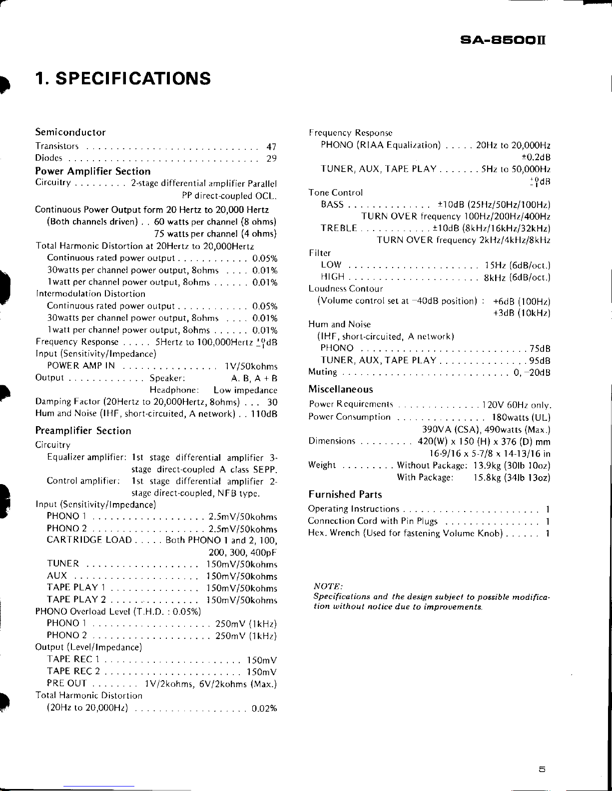
1.
SPECIFICATIONS
Semiconductor
Transistors
.....47
Diodcs..
......29
Power
Amplifier Section
Circuitry
.
2-stagc differenrial
amplifier
parallcl
PP direct-coupled
OCL.
Continuous Power
Output form 20 Hertz to 20,000 Hertz
(Both
channels driven)
. . 60
watts
per
channel
(8
ohms)
75 watts
per
channel
(4
ohms)
Total Harmonic Distortion
at 20Hertz to 20,000Hertz
Continuousratedpoweroutput
.... 0.O5o/o
3owatts
per
channcl
power
output,8ohms
. . . . 0.01y.
I watt
per
channel
power
output, 8ohms
. . . . . . 0.01%
lntermodulation Distortion
Continuous rated
power
output
. . . 0.05%
3owatts
per
channel
power
output,8ohms
. . . . 0.01%
I watt
pcr
channel
power
output, 8ohms
. . . .
. . 0.01y.
Frequency
Respon5c
.. . . . 5Hertzto 100,000Herrzl0,dB
lnput
(Sen
sitivity/
lm
pedance)
POWERAI\4PlN
.....
... 1V/5Okohms
Output..
.. Speaker:
A.B,A+B
Preamplifier
Section
Circu itry
Equalizer
amplifier: lst
stage differential
amplifier
3-
stage direct-coupled
A class SEPP.
Control amplifier: lst
stage differential
amplifier 2-
stagc direct-coupled, NFB
type.
Input
(Sensitivity/l
mpcdance)
PHONOl
.
. .
2.5mV/50kohms
PHONO2
. . . 2.5mV/50kohms
CARTRIDGE LOAD.
. . . . Both PHONO
I and 2, 100,
200,300,400pF
TUNER
.
.. 150mV/50kohms
AUX ...
.. 150mV/50kohms
TAPEPLAY1......
15OmV/5Okohms
TAPEPLAY2........
l50mV/5okohms
PHONO
Overload Level
(T.H.D.
:0.05%)
PHONO L
...250mV(1kHz)
PHONO2
....250mV(1kHz)
Output
(Level/
lm
pedance)
TAPEREC1......
150mV
TAPEREC2......
.........'l50mv
PRE
OUT
lv/2kohms,
6V/2kohms
(Max.)
Total Harmonic Distortion
(20H2
to
20,000H2)
......
..... o.o2.A
Frequency Responsc
PHONO
(RIAA
Equalization)
TUNE
R, AUX, TAPE PLAY
Filter
LOW
... ...
... .
H|GH..........
Loudness
Contou r
(Volume
control set at
sA-a5ClC'II
20Hz to 20,000H2
t0.2dB
. 5Hz to 50,000H2
j
?dB
Tone Control
BASS... ...
r10dBl25Hzl5l9zll01Hz)
TU RN OVER frequency 1Q0Hzl200Hzl4O0Hz
TREBLE.
...i10d8(8kHzl'l6k9zl32k1z)
TURN OVE R frequency 2kHzl4kHzlSkHz
... 15Hz
(6dB/oct.)
. .
8kHz
16d
B/oct.)
40dB
position) : +6dB
(100Hr)
+3dB (1okHz)
Hum
and
Noise
(lH
F,
short-circuited,
A network)
PHONO.
TUNER,
AUX, TAPE PLAY
. . .
l\4uting
..
M iscellaneous
Power
Rcquiremcnrs
120V 60Hz only.
Powcr
Consumption
l80watts
(UL)
390VA
(CSA),
490watts
(Max.)
Dimensions
. a20(W)
x 150
(H)
x
376
(D)
mm
16-9116 x 5-118 x 14-13116
in
Weighl
. . Without Package:
13.9kg
(301b
l0oz)
With
Package:
15.8kg
(341b
13oz)
Furn
ished Parts
Operating
Instructions
.......1
Connection
Cord
with
Pin Plugs
........1
Hcx. Wrench
(Used
for
fastening Volume
Knob) . . . . . .
'l
NOTE:
Specificotions
ond the design
subject to
possible
modifica-
tion
u,ithout notice due
to improuements.
...75d8
. . . 95dB
0,20d8
I
Headphone:
Low
impeddnc
c
r
Damping I dclor
(20Hert1
lo 20.000Hcrt./,
8oh m:) .
. . 30
Hum
and Noise
(lHF,
short-circuited,
A network) . . 110d8
!
p
Page 5
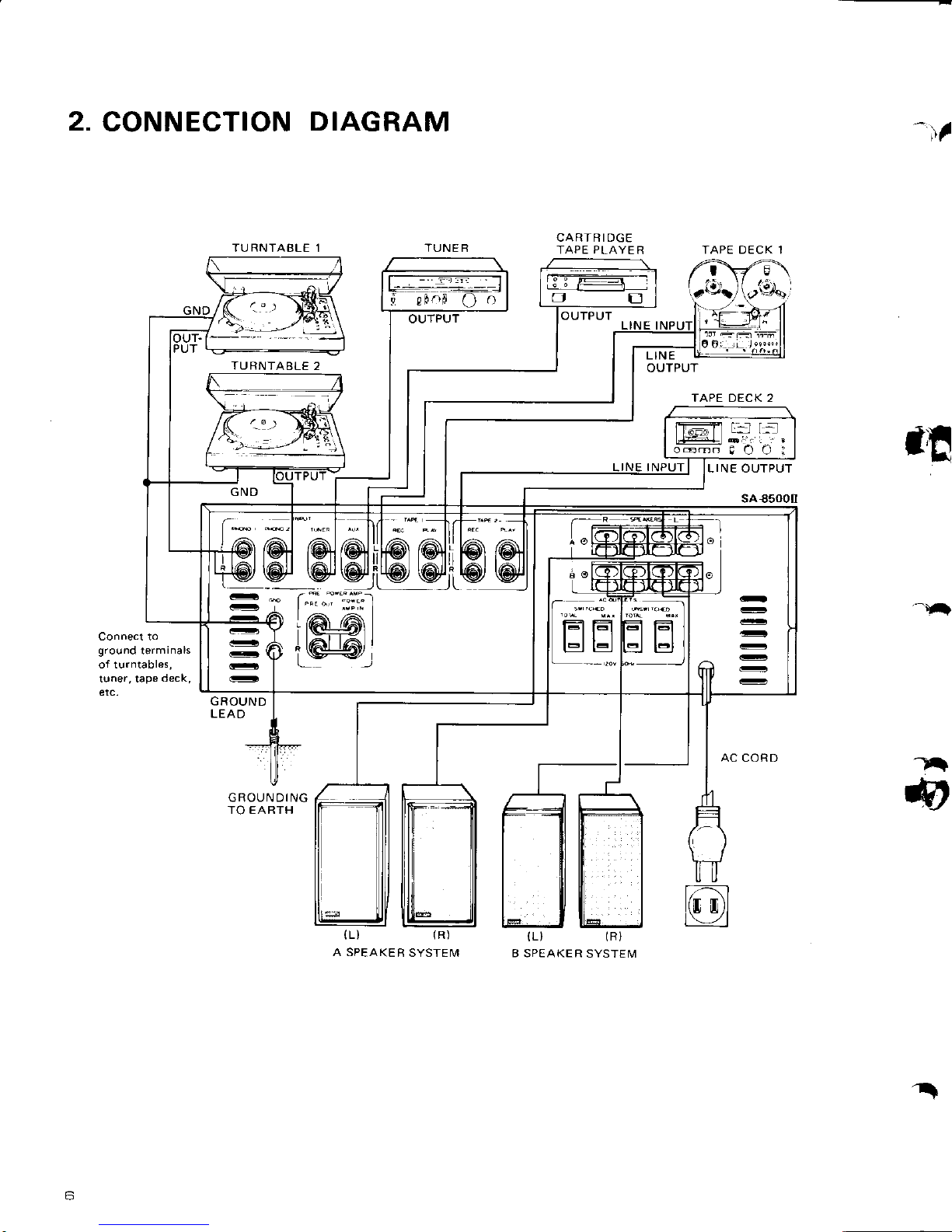
2.
CONNECTION
DIAGRAM
TU RNTABLE 1 TUNE R
TU RNTABLE
2
'r'l
CARTRIDGE
TAPE PLAYE
R
TAPE DECK 2
JU
-n
Connect to
ground
terminals
etc.
GROUND
LEA
D
GROUNDING
TO EARTH
F
@
A SPEAKE
R SYSTEM
B SPEAKE R
SYSTEM
I
Page 6
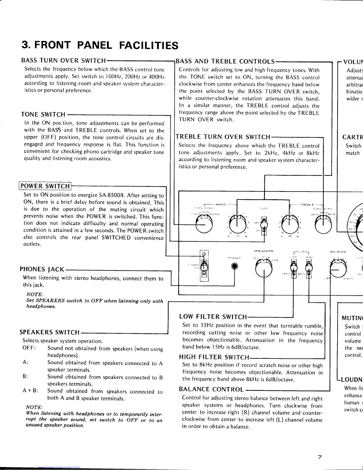
3.
FRONT
PANEL
FACILITIES
BASS TURN
OVER SWITCH
Selects
the frequency
below
which
the BASS
controt
tonc
adjustments
apply.
Ser
swirch to 100H2,
200H2
or 40OHz
according to
listening
room
and speaker
system
character-
istics or
personal preference.
TONE
SWITCH
ln the
ON
pos;tion,
tone adjustments
can be
performed
with the BASS
and
TREBLE
controls.
When
set to the
upper
(OFF) position,
the tone
control
circuits
are dis-
engaged
and frequency
response
is flat.
This function
is
convenient
for
checking
phono
cartridge
and speaker
tone
quality
and listening
room
acoustics.
Set to ON
position
to energize
54-850011.
After
setting
to
ON,
there
is a brief
delay
before
sound
is obtained.
This
is
due
to the
operation
of the
muting circuit
which
prevents
noise when
the PowER
is
switched.
This func-
tion does
not
indicate
difficulty
and
normal
operating
condition
is attained
in a few
seconds.
The POWER
switch
also
controls
the rear
panel
SWITCHED
convenience
outlets.
PHONES
JACK
When
listening
with
stereo
headphones,
connect
them
to
this
jack.
NOTE:
Set SPEAKERS
switch
to OFF
when listening
only with
headphones.
SPEAKERS
SWITCH
Selects
speaker
system
operation.
OFF:
Sound
not obtained
from
speakers
(when
using
headphones).
A:
Sound
obtained
from
speakers
connected
to A
speaker
terminals.
B:
Sound
obtained
from
speakers
connected
to B
speakers
terminals.
A+B:
Sound
obtained
from
speakers
connected
to
both
A
and B
speaker
terminals.
NOTE:
When
listening
with
headphones
or
to
temporarily
inter-
rupt
the
speaher
sound, set
switch
to OFF
or to
an
unused
speaher
position.
BASS
AND TREBLE
CONTROLS
Controls for
adlusting
low and high
frequency
tones.
With
the TONE
switch
set to ON,
turning the
BASS
control
clockwise
from
center enhances
the frequency
band below
the
point
selected
by the BASS
TURN
OVER
switch,
while
counter-clockwise
rotation
attenuates
this band.
In
a sinrilar
manner,
the
TREBLE
control
adjusts
the
frequency
range
above
the
point
selected by
the
TREBLE
TURN
OVER
switch.
TREBLE
TURN
OVER
SWITCH
Selects
the frequency
above
which
the TREBLE
control
tone adjustments
apply.
Set to
2kHz, 4kHz
or SkHz
according
to
listening
room and
speaker
system character-
istics
or
personal
preference.
t'-""1
LOW FILTER
SWITCH
Set
to 15Hz
position
in the
event
that turntable
rumble.
recording
cutting
noise
or
other low
frequency
noise
becomes
ob
jectionable.
Attenuation
in
the frequency
band
below
15Hz
is
6dB/octave.
HIGH
FILTER
SWITCH
Set
to 8kHz
position
if record
scratch
noise
or other
high
frequency
noise
becomes
objectionable.
Attenudtion
in
the frequency
band
above
8kHz
is
6dB/octave.
BALANCE
CONTROL
Control
for
adjusting
stereo
balance
between
left
and right
speaker
systems
or
headphones.
Turn
clockwise
from
center
to
increase
right
(R)
channel volume
and
counter-
clockwise
from
center
to
increase
left
(L)
channel volume
in
order
to obtain
a balance.
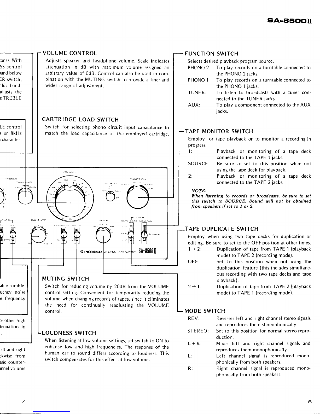
VOLUI
Adf
usts
atten
ua
arbitrar
b inatior
wider
r
CARTR
Switch
match
I{
t--
I
MUflN(
I
Switch I
I
control
I
volume
I
the ne(
I
controt.
I
I
LLOUDN
When
lis
enhance
numan
(
switch
c(
7
POWER
SWITCH
Page 7
lones.
With
SS control
)and below
5R
switch,
this band.
idjusts
the
E TREBLE
LE
control
z or
8kHz
I character-
f'-"''r
able rumble,
uency
noise
e frequency
rr other
high
tenuition
in
left
and right
ckwise from
and counterlnnel volume
CARTRIDGE
LOAD
SWITCH
Switch
for
selecting
phono
circuit
match
the load
capacitance
of the
input
capacitance
to
employed
cartridge.
VOLUME
CONTROL
Adlusts
speaker
and headphone volume.
Scale
indicates
attenuation
in dB with
maximum
volume
assigned an
arbitrary
value
of 0dB.
Control can also
be used in
com-
bination
with
the MUTING
switch to
Drovide
a finer
and
wider
range of
adjustment.
sA-A5Clcltr
FUNCTION SWITCH
Selects
desired
playback program
source.
PHONO 2: To
play
records on a turntable connected to
the
PHONO
2
jacks.
PHONO 1 : To
play
records on a
turntable
connected
to
the PHONO
1
iacks.
TUNER: To listen
to broadcasts
with
a tuner con-
nected to the TUNER
iacks.
AUX: To
play
a
component
connected to the AUX
iacks.
TAPE MONITOR SWITCH
Employ for tape
playback
or to monitor a recording
in
progress.
1
: Playback
or monitoring
of a tape
deck
connected to the TAPE 1
jacks.
SOURCE:
Be sure to set to this
position
when not
using the tape deck for
playback.
2:
Playback
or
monitoring
of a tape deck
connected to the TAPE 2
iacks.
NOTE:
When listening to records or broadcasts, be
sure to set
this switch to
SOURCE. Sound
will
not
be obtained
from
speahers if set to I or 2.
TAPE DUPLICATE
SWITCH
Employ when using two tape decks for
duplication or
editing. Be sure
to set to
the
OFFposition at other times.
1
-->
2: Duplication of tape
from TAPE 1
(playback
mode)
to T APE 2
(recording
mode).
OFF:
)
T'"-'-l
(0
rrrorueen
IEREO AMPL
$A-8500
[
MUTING
SWITCH
Switch for
reducing volume
by 20dB from
the
VOLUME
control
setting. Convenient
for temporarily
reducing the
volume when
changing records
of tapes,
since
it
eliminates
the
need for
continually read
justing
the VOLUME
control.
OUDNESS
SWITCH
When listening
at low volume
settings,
set switch to ON to
enhance
low
and high frequencies.
The response
of the
human
ear
to sound differs
according to
loudness. This
switch
compensates
for
this effect at low volumes.
Set to this
position
when not using
the
duplication feature
(this
includes simultane-
ous recording
with two tape decks and tape
playback).
Duplication of tape from TAPE
2
(playback
mode) to TAPE 1
(recording
mode).
SWITCH
Reverses left
and right channel stereo signals
and reproduces them stereophonically.
2- 1:
MODE
REV:
STEREO: Set to this
position
for
normal
stereo repro-
duction.
L
+
R:
Mixes
left and
right channel signals
and
reproduces them monophonically.
L: Left
channel signal
is reproduced
mono-
phonically
from both speakers.
R:
Right channel
signal is
reproduced
mono-
phonically
from both speakers.
Page 8
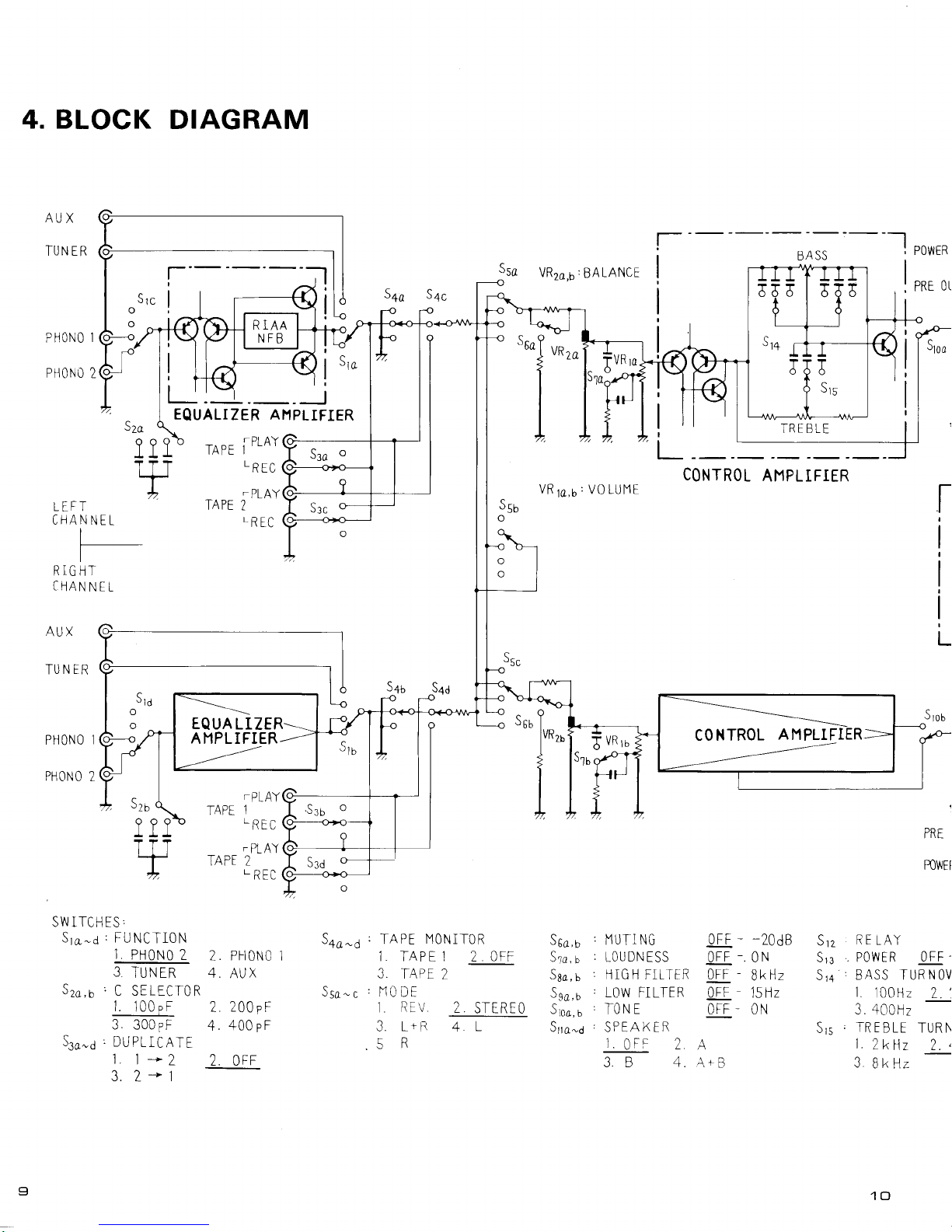
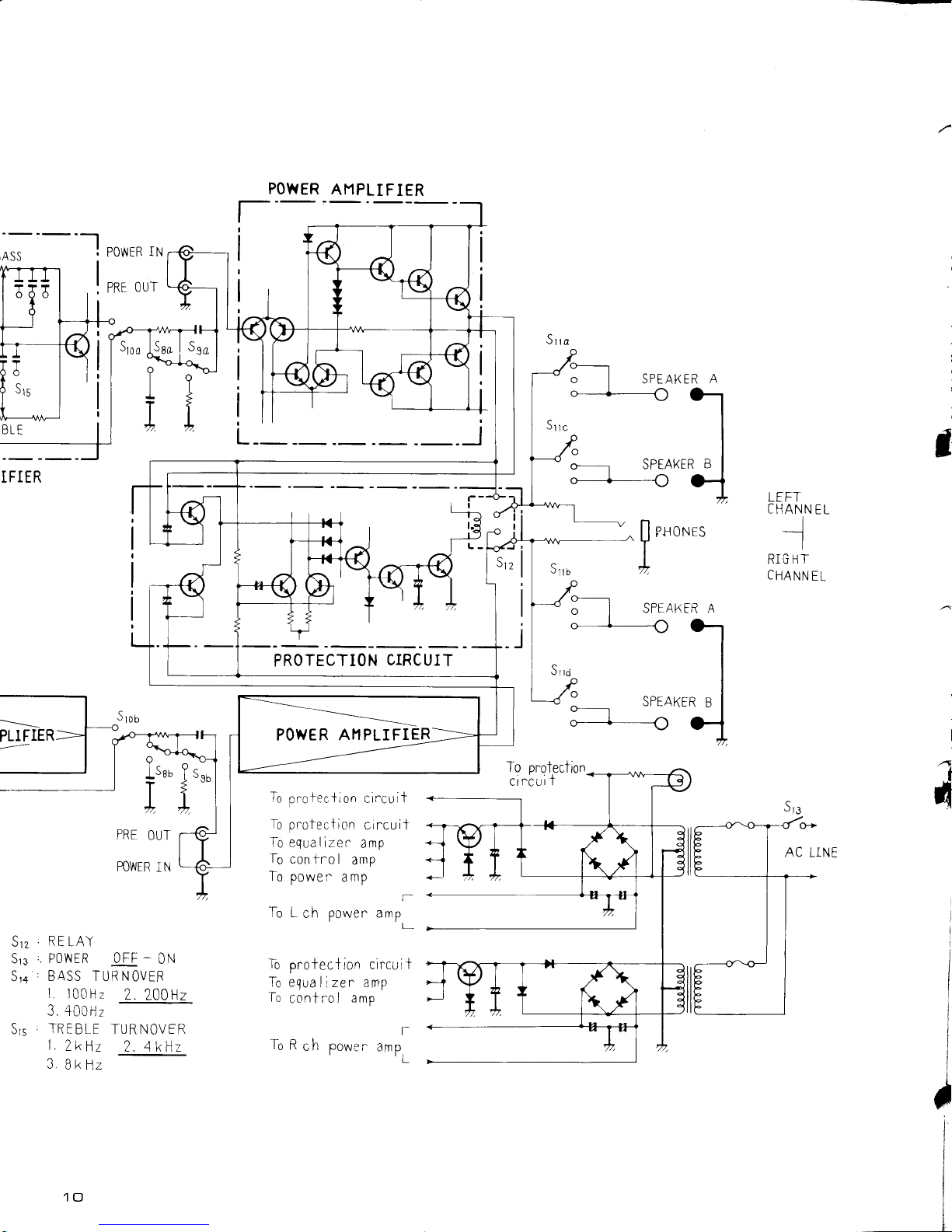
4. BLOCK
DIAGRAM
Ssa
o
S+a-d ' TAPE
MONITOR
1. TAPEI 2 OFF
3.
TAPE
2
Ssa-c
,X0DE
1
REV
3.
LrR
.5
R
2
STEREO
I oncc
I
POwrn
BA
SS
PRE
OL
TREBLE
CONTROL
AMPLIFIER
l-
L
PRE
POWEF
tt
SV'JITCH ES
,
Sra-d'FUNCTI0N
t.
PH0N0
2
3
TUNER
Szo,b,C
SELECIOR
1.
100pF
3.
300pF
S3o-d,DUPLICATF
l.
l*2
3.2*1
sqc
s+a
Ssa
VRza,b
,
BA
LANCE
VR
ra,u'
V0 LUIIE
6
VRru
c^
rbo,b
Sra,
s
Sao,
u
Sso,
o
Stoo,
u
'
IlUTI NG
:
TOUDNESS
'
HIGH
FITIER
'
LOW
FILTER
.TONE
'SPEAKER
]
OFF
?
3 B 4.
OFF
- -20d8
OFF
_.
ON
OFF
-
BkHz
OFF
15 Hz
OrF - 0N
A
A+B
Srz
RE
LAY
S13
.
POWER OFF
-
S1a
'
BASS TUR N 0V
I
100H2
7.',
a / ^^ |
J..tLrul.'17
Sl5,TREBLE
TURN
1.
Tk\z
l.
z
3
BkHz
PHONO
1
PH(')NO
2
AUX
TU
N FR
LEFT
CHANNEL
RIGHT
CFIANNET
EQUALIZER
AI'lPLIFIER
"l
-"
1t1
v
TAPE
|PLAY
LREc
-
PLAY
TAPE
2
LREC
J
q^^
Sno
5+u
"9
o6b
I
I
vRto
I
c
J2i)
.PLAY
TAPE
1
.REC
.
PL A'l
TAPE 2
LREC
2 . Pr-10N0
1
4.
AUX
2
200pF
4.
400pF
2. OFF
EQUA
LIZER
AIlPLIFIER
CONTROL
AHPLIFIER
4
L
Srra-a
Page 9
.
RE
LAY
..
POIIER OFF
-
ON
.
BASS TURNOVER
1.
l00Hz
2.200H2
3.400H2
TREBLF
TURNOVER
1.
LkHz
2. 4kl,z
3.
BkHz
PO
r-
WER
AI1PLTFIER
L
PROTECTION
CIRCUIT
To
pnotection
clr^cuit
To
pnotection
cir cuit
To equalizer^
amp
To
con
f
r-o I
amp
To powen
amp
r
To
L
ch
powen ampl
proteclron
cir cuit
eguallzen
amP
Contr0
I
amP
T
To
R
ch
powen ampL
e
u9o
c
JIo
o
8a
ls
I
T
J
J
T
FIER
LEFT
CHANN
EL
I
I
RIG HT
CHANNEL
f
rloru,s
SPEAKFR A
?e
*
"sb
I
e
ISeu
T
I
)-
PRE
OUT
POWER
IN
To
pr
otection
cir-cuit
;
I
c
e13
CP
AC
LTNE
Srz
Srs
a
u14
r0
To
To
i
I
i
I
,
POWER
AIlPLIFIER
Srs
Page 10
A
5. CIRCUIT
DESCRIPTIONS
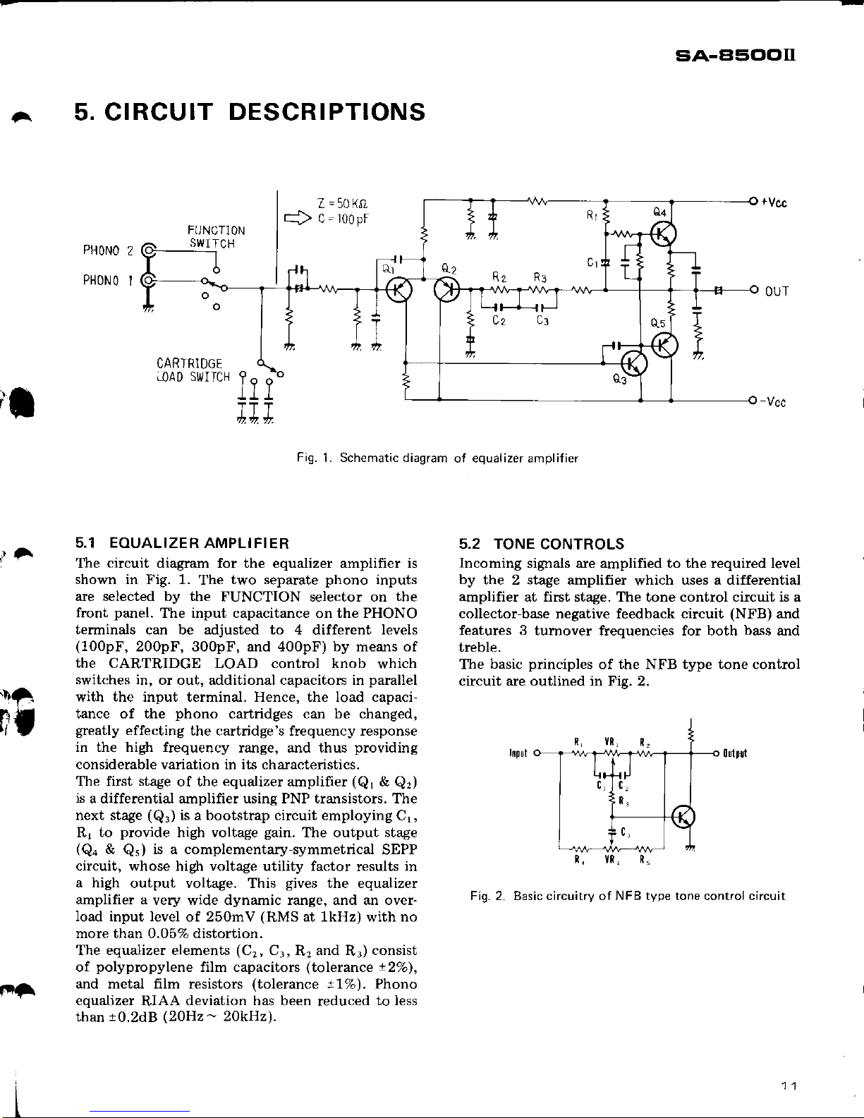
z=50Krt
c)
c=roopr
PHONO
2
PHONO
I
CARTRIDGE
LOAD SWITCH
sA-El5ClClII
-vcc
+
lr.
rl
Fig.
L Schematic diagram
of equalizer amplifier
,li
5.1 EOUALIZER
AMPLIFIER
The
circuit
diagram for the equalizer amplifier is
shown in Fig. 1.
The
two separate
phono
inputs
are selected by the
FUNCTION selector on
the
front
panel.
The input capacitance
on
the PHONO
terminals can be adjusted to 4
different
levels
(100pF,
200pF, 300pF, and 400pF) by means of
the
CARTRIDGE LOAD control knob
which
switches in,
or out, additional capacitors in
parallel
with the input terminal. Hence, the load capacitance of the
phono
cartridges can be changed,
greatly
effecting
the cartridge's frequency response
in the high frequency
range, and thus
providing
considerable variation in its characteristics.
The first stage
of the
equalizer
amplifier
(Q'
&
Qr)
is
a differential amplifier using PNP transistors. The
next stage
(Q.)
is a bootstrap circuit employing
C'
,
R1 to
provide
high voltage
gain.
The output stage
(Qo
&
Qr)
is a complementary-symmetrical
SEPP
circuit, whose high voltage
utility
factor
results
in
a high
output voltage. This
gives
the equalizer
amplifier a
very wide dynamic range, and an over-
Ioad input level
of 250mV
(RMS
at lkHz) with no
more than 0.05% distortion.
The equalizer elements
(Cr,
C.,,
R,
and
R.)
consist
of
polypropylene
film capacitors
(tolerance 127o),
and metal frlm resistors
(tolerance
t1%).
Phono
equalizer
RIAA
deviation has been
reduced
to less
than
10.2dB
(2OHz
-
2OkHz\.
5.2
TONE
CONTROLS
Incoming
signals are amplified to the required level
by
the 2 stage amplifier
which
uses a differential
amplifier at first stage. The tone control circuit is a
collector-base negative
feedback
circuit
(NFB)
and
features 3
tumover frequencies for both
bass
and
treble.
The
basic
principles
of the NFB type tone control
circuit are outlined in Fis. 2.
'fl
h
rl
0d0ut
hI|lt
n, vn,
n,
L.-
,,,
-{P
c.
Rl
,c.
d
Fi1. 2.
t, vR, R,
Basic circuitry of
NFB
type tone control circuit
iri
Page 11
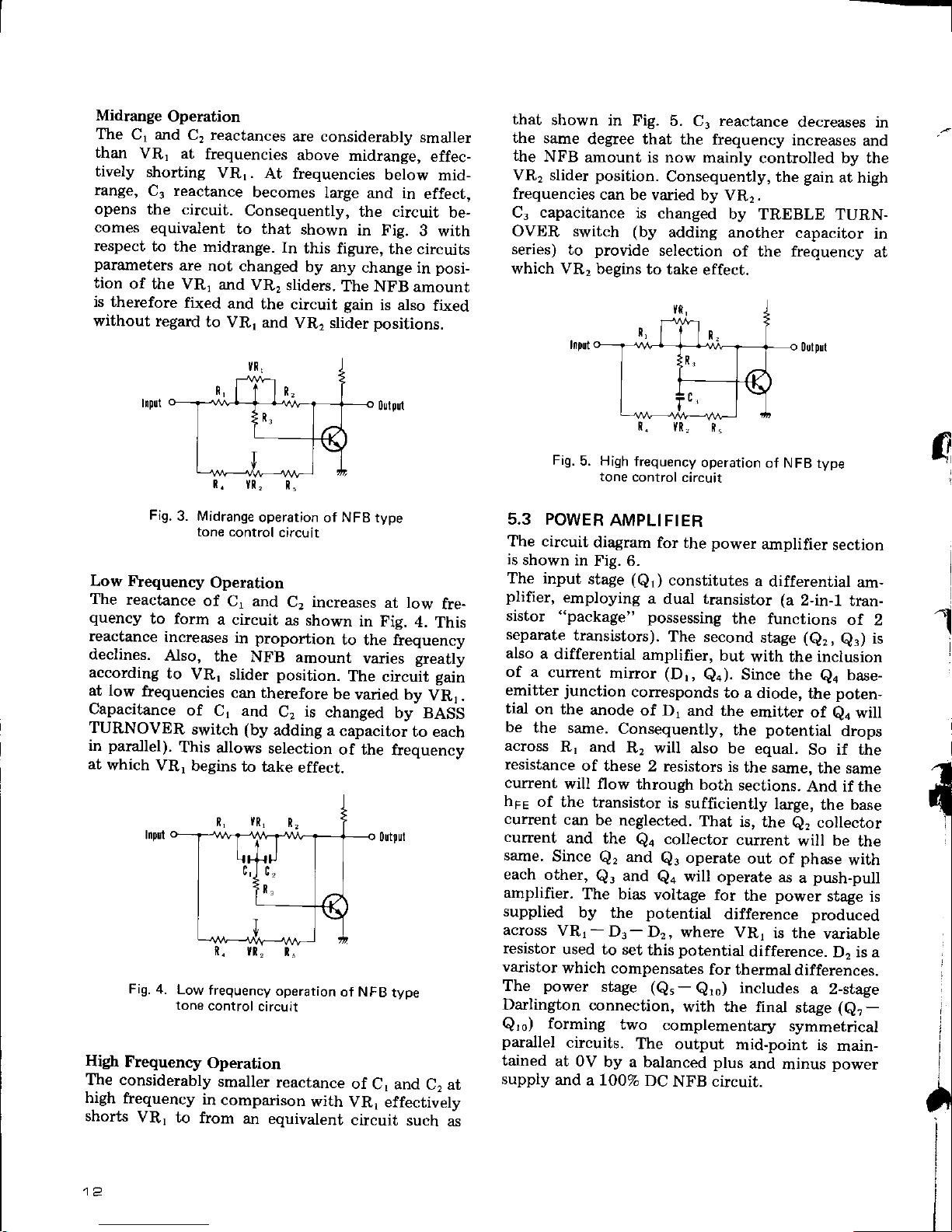
Midrange
Operation
The
Cr and
C, reactances
are considerably
smaller
than
VRr at
frequencies
above
midrange,
effec-
tively
shorting
VRr.
At frequencies
below
mid-
range,
C. reactance
becomes
large
and in
effect,
opens
the circuit.
Consequently,
the circuit
be-
comes
equivalent
to that
shown
in Fig.
3
with
respect
to the
midrange.
In
this
figure,
the circuits
parameters
are
not changed
by any
change in
pos!
tion
of the
VR, and
VR.
sliders.
The NFB
amount
is therefore
fixed
and
the circuit gain
is also
fixed
without
regard
to VRr
and
VR, slider
positions.
Fig.
3. Midrange
operation
of
NFB
type
tone control
circuit
Low Frequency
Operation
The
reactance
of
C, and
C, increases
at low
fre-
quency
to form
a circuit
as
shown
in Fig.
4.
This
ipactance
increases
in proportion
to the
frequency
declines.
Also,
the
NFB
amount
varies
grea
y
according
to
VR1
slider
position.
The
circuit
sain
at low
frequencies
can therefore
be
varied by
Vh1.
Capacitance
of
C1 and
C,
is
changed
by BASS
TURNOVER
switch
(by
adding a
capacitor
to each
in
parallel).
This
a.llows
selection
of the
frequencv
at
which
VR, begins
to take
effect.
that
shown
in Fig.
5. C. reactance
decreases in
the
same
de$ee that
the frequency
increases
and
the
NFB
amount is now mainly
controlled by the
VR, slider
position.
Consequently,
the
gain
at high
frequencies
can be
varied by
VR:.
C. capacitance
is changed
by
TREBLE TURN-
OVER switch
(by
adding another
capacitor
in
series)
to
provide
selection
of the frequency
at
which
VR: begins
to take
effect.
Fiq.
5. High
frequency
operation
of NFB
type
tone
control
circuit
5.3 POWER
AMPLIFIER
The circuit
diagram
for the
power
amplifier
section
is
shown
in
Fig. 6.
The input
stage
(Q1)
constitutes
a
differential
am-
plifier,
employing
a
dual transistor (a
2-in-1
tran-
sistor
"package"
possessing
the
functions
of
2
separate
transistors).
The
second
stage
(er,
e.)
is
also
a differential
amplifier,
but
with the inclusion
of a
current
mirror
(D1,
Qr).
Since the
ea
base-
emitter
junction
conesponds
to a diode,
the
poten-
tial
on the
anode
of D,
and the
emitter
of
eo
will
be
the same.
Consequently,
the
potential
drops
across
R, and
R, will
a.lso be
equal.
So if the
resistance
of these
2 resistors
is
the same,
the same
current
will flow
through
both
sections.
And if the
hpg
of
the transistor
is sufficiently
large,
the base
current
can
be
neglected.
That
is, the
e.
collector
current
and
the
Qa
collector
current
will
be
the
same.
Since
Q,
and
Q3
operate
out
of
phase
with
each
other,
Q:
and
Qo
will
operate as
a
push-pull
amplifier.
The bias
voltage
for
the
power
stage
is
supplied
by
the
potential
difference produced
across
VR1
-
D3
-
D,
,
where VR1
is the
variable
resistor
used to
set this
potential
difference.
D, is a
varistor
which
compensates
for thermal
differences.
The
power
stage
(Qs-
Q16)
includes
a 2-stage
Darlington
connection,
with
the fina.l
stage
(e7-
Qto)
forming
two
complementary
symmetrical
parallel
circuits.
The
output
mid-point is
main-
tained
at 0V
by a balanced plus
and
minus
power
supply
and
a 700%
DC
NFB circuit.
f
)
I
'l
l
fr
vn.
Fig.
4. Low
frequency
operation
of NFB
type
tone
control
circuit
High
Frequency
Operation
The considerably
smaller
reactance
of
C, and
C" at
high
frequency
in
comparison
with
VR,
effectivelv
shorts
VR,
to
from
an
equivalent
circuit
such
as
Page 12
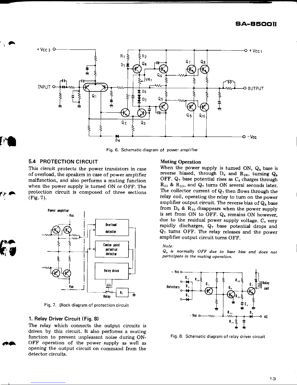
-r
''r
i
sA-aE'ootr
+vcc1
OUTPUT
+vcc2
INPUT
ft.'f
r\i'^
5.4 PROTECTION
CIRCUIT
This circuit
protects
the
power
transistors in
case
of
overload, the speakers
in case
of
power
amplifier
malfunction,
and also
performs
a
muting function
when the
power
supply is tumed
ON or
OFF. The
protection
circuit is composed
of three sections
(Fis.7).
Por!r.r||0lili!r
Fig. 7.
Block diagram
of
protection
circuit
1. Relay Driver
Circuit
(Fig.
8l
The
relay which connects
the output circuits is
driven
by this circuit. It
also
performs
a muting
function
to
prevent
unpleasant noise during
ON-
OFF operation
of the
power
supply
as well as
opening the
output circuit on command
from the
detector
circuits.
04
Fig. 6. Schematic diagram
of
power
amplifier
Muting
Operation
When the
power
supply
is
tumed
.ON,
Qu
base is
reverse biased,
through
D6 and
R26, turning
Qo
OFF.
Q?
base
potential
rises
as Ca charges
through
R22 & Rz3, and
Q?
turns
ON several
seconds
later.
The collector
current
of
Q7
then
flows
through
the
relay coil,
operating
the
relay to tum
on the
power
amplifrer
output circuit.
The
reverse bias
of
eu
base
from
Du
&
R2o
disappears
when the
power
supply
is set
from
ON to
OFF.
Qu
remains
ON however,
due
to the residual power
supply
voltage. Ca
very
rapidly
discharges,
Q,
base
potential
drops
and
Q?
tums
OFF.
The relay
releases
and the
power
amplifier
output
circuit
turns
OFF.
Note:
Q"
is
normally
OFF due
to base
bias
and does
not
participate
in
the
muting operction.
{tr-
Fig.
8. Schematic diagram
of relay driver circuit
Page 13
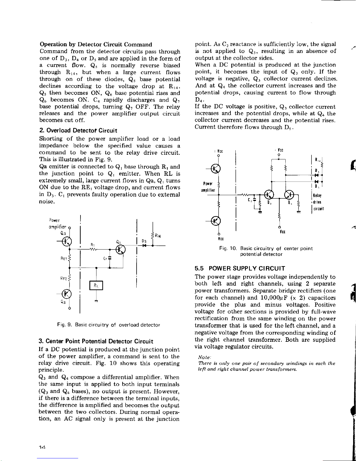
Operation by Detector
Circuit Command
Command from
the detector
circuits
pass
through
one of D., Do or
D, and are applied in the form
of
a current
flow.
Q5
is normally
reverse biased
through
R1a,
but
when a large current flows
through
on of these diodes,
Q,
base
potential
declines according
to the voltage drop
at R,a.
Q,
then
becomes
ON,
Qu
base
potential
rises and
Qu
becomes
ON. Co rapidly
discharges and
Q,
base
potentia.l
drops, tuming
Q?
OFF. The relay
releases
and the
power
amplifier output circuit
becomes cut
off.
2.
Overload Detecto? Circuit
Shorting
of the
power
amplifier load
or a load
impedance
below the specified
value causes a
command
to be sent to
the relay drive circuit.
This is illustrated
in Fig.
9.
Qa
emitter is connected
to
Q,
base
through
R,
and
the
junction
point
to
Q,
emitter.
When
RL
is
extremely small, Iarge current flows
in
Qa, Q,
turns
ON
due
to the
RE,
voltage
drop, and current flows
in
D.. C1
prevents
faulty operation
due to extemal
norse.
oirplifier
eq
Fig.
9. Basic
circuitry
of
overload detector
3. Center Point Potential
Detector Circuit
If
a DC
potential
is
produced
at the
junction
point
of the
power
arnplifier, a
command is sent to the
relay drive circuit.
Fig. 10 shows
this operating
principle.
Qr
and
Qo
compose
a differential amplifier.
When
the
same input is
applied to both input
terminals
(Q.
and
Qo
bases),
no
output
is
present.
However,
if there
is a difference between
the terminal inputs,
the
difference is amplified
and becomes the
output
between
the two collectors.
During normal
opera-
tion, an
AC signal only is
present
at the
junction
point.
As Cr reactance is
sufficiently
low,
the signal
is not applied to
Q3,
resulting in
an
absence of
output at the collector sides.
When a DC
potential
is
produced
at the
junction
point,
it becomes
the input of
Q.
only. If the
voltage
is negative,
Q.
collector current declines.
And at
Qo
the collector current increases and the
potential
drops, causing current to flow through
If the
DC voltage is
positive,
Q.
collector
current
increases
and
the
potential
drops,
while at
Qo
the
collector current
decreases
and
the
potential
rises.
Current therefore flows
through D. .
Fig- 10.
Basic circuitry
of
center
point
potential
detector
5.5 POWER SUPPLY
CIRCUIT
The
power
stage
provides
voltage
independently
to
both left
and right channels, using 2 separate
power
transformers.
Separate
bridge
rectifiers
(one
for each
channel) and 10,000gF
(x
2) capacitors
provide
the
plus
and
minus voltages. Positive
voltage for
other
sections
is
provided
by full-wave
rectification from the same
winding on the
power
transformer
that is used for
the
left
channel, and a
negative
voltage from the corresponding
winding of
the right channel
transformer. Both are supplied
via voltage
regulator circuits.
There
is only one
pair
of
secondary
windings in each
the
lcfl and righl
channel
powcr
lrans[ormcrs.
t
{
Page 14
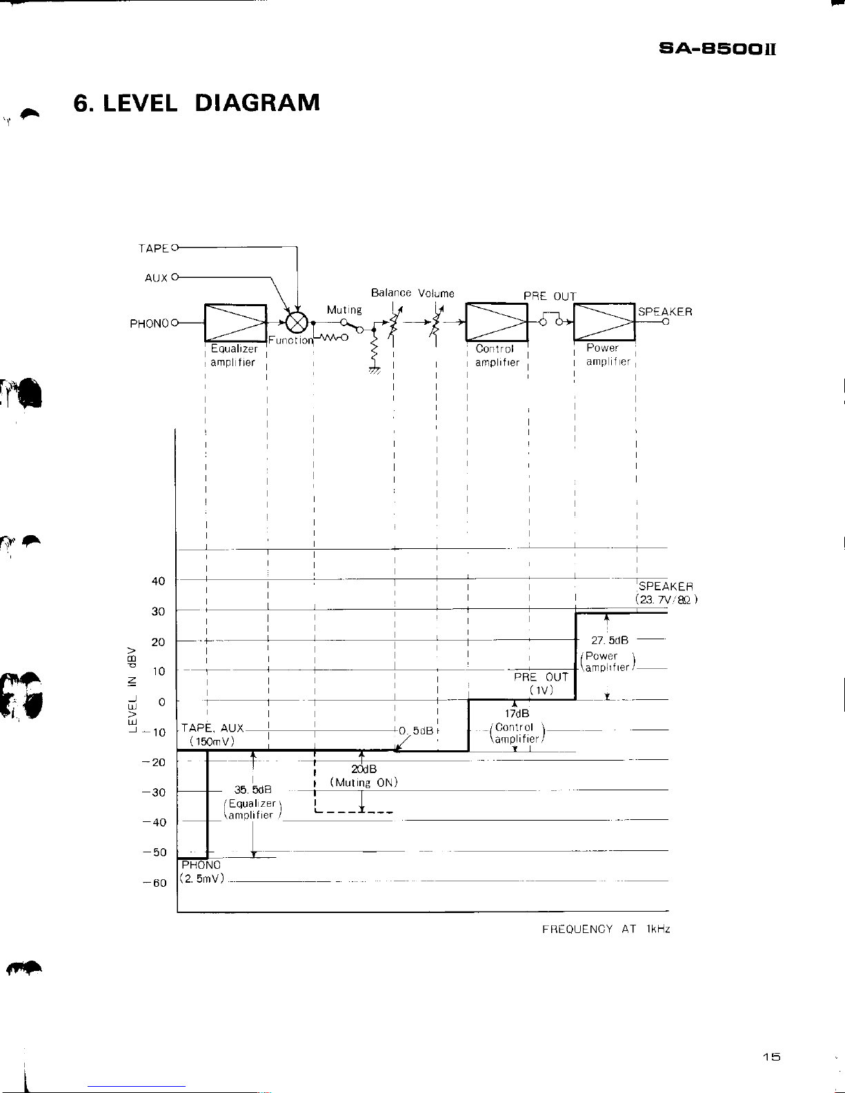
6.
LEVEL
DIAGRAM
siA-E'5clclil
SPEAKER
't
A
PRE
OUT
PRE OUT
(
1V)
-
-SPEAKEF
(23.7v,
&) )
amp 1er
f\il
|
[*i
.D
1
d
J-
20
10
0
10
-20
30
50
-60
27. 5dB
/Power l
\afn0lrlrer/
lf
35.5dB
iEqual
zer
\
\amplrfrer
/
r
(Muting
ON)
17d B
APL. AU\
.r0 5oB
/r5O,rV)
./
/Control \
\am
plif
re r
/
(2.
5mv)
tzel
I rer
FREOUENCY
AT lKHZ
rtf
Page 15
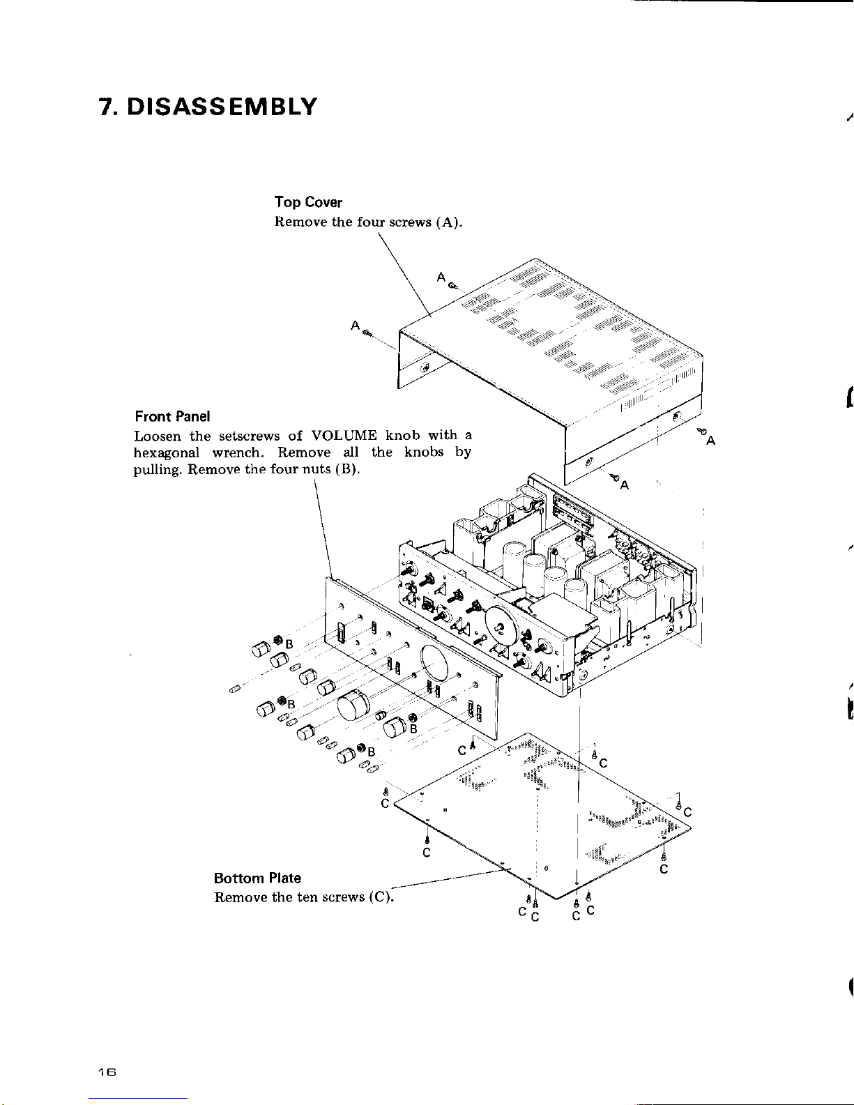
7.
DISASSEMBLY
Top Cover
Remove the four screws
(A).
Front Panel
Loosen the
setscrews of VOLUME
knob with
a
hexagonal wrench. Remove
all
the knobs
by
pulling.
Remove
the
four nuts
(B).
Bottom
Plate
Remove
the ten screws
(C).
Page 16

Control Amplifier Assembly
Remove
the
three screws
(D).
Power Amplifier
Block
(L)
Remove
the
three
screws
(E).
CtA-E'5clC'tr
Power Amplif
ier
Block
(Rl
Remove
the
three screws
(F).
Equalizer
Amplif ier Assembly
R€move
the two
screws
(G).
Switch Assembly
Remove
the seven screws
(H).
17
Page 17
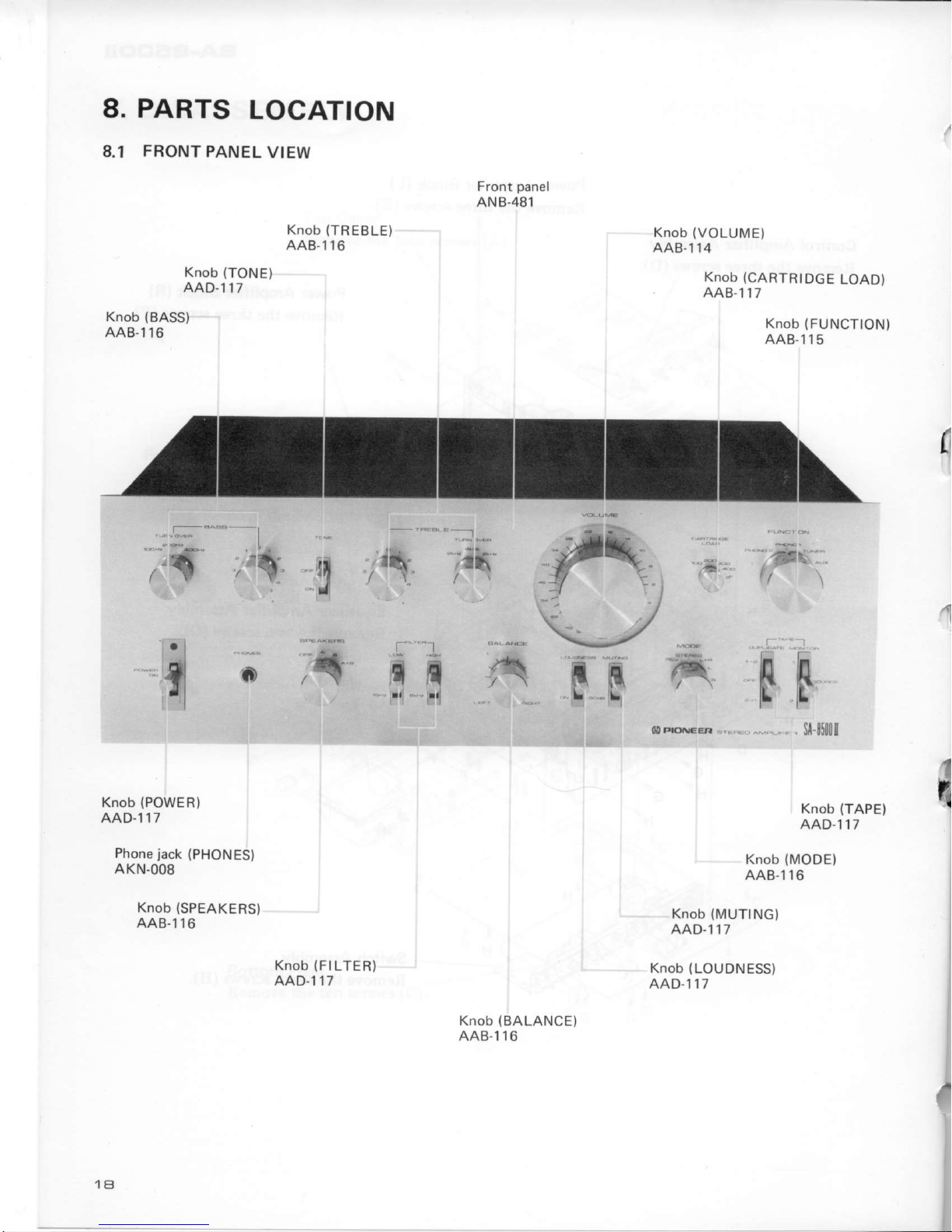
8.
8.1
PARTS
LOCATION
FRONT
PANEL
VIEW
Knob
(TR
E B LE)
AAB.1 16
Front
panel
ANB.481
Knob
(TONE)
AAD-117
Knob
{BASS)
AA8.1r6
Knob
(VOLU|\ilE)
AAB 1 14
Knob
(CART
R tDG
E
LOAD)
AAB 117
Knob { FUNCTION}
AAB.1 1
5
;'ry;[
::|l
-iiq'
tr'
;l
(
I
o
Knob
(POWE
R
)
AAD-1 I7
Phone
jack
(PHON
ES)
AKN-OO8
Knob
(SPEAKERS)
AAB.l
16
.:
..r
FF
.,,,,
.."., ,
ile5001
,l
.r"'.1
il[
-.Frl -"F!
tn
]L.",,!
Knob
(TApE)
AAD-1 17
Knob
(l\4ODE)
AAB.1 16
Knob
(MUTING)
AAD.1
1 7
Knob
{LOUDNESS)
AAD.l 1 7
7
(
Knob
(F
ILTE
R
)
AAD.117
Knob
(BALANCE)
AAB.I16
I
Page 18

a-
I
8.2
FRONT V|EW WtrH
PANEL REMOVED
SA-BSOOII
Rotary switch
(CARTR
IDGE LOAD)
ASD,065
(ASD-055)
Rotary switch
(FUNCTTON)
ASD,052
Lever switch
(TO
N E)
ASK
109
Variable resistor
(BASS)
ACV 136
Rotary switch
(BASS
TURNOVER
)
ASD 057
Rubber bracket
AEB-092
Rotary switch
(TREBLE
TU RNOVE R
)
ASD.O56
Variable
resistor
(VO
LU
I\4
E)
ACV,171
I
Variable resistor
(TREBLE)
ACV-136
a),
)
'f;.
J
r:
'
ar,r,o,,
'g)
tt
E.E./.iJ
nno.(,
I T
E.
nsl
Lever
switch
(POWER)
ASK.1
24
Lamp
with leads
BV,
50mA
AE L
081
Phone
jack (PHON
ES)
AKN
OOB
Rotary switch
(SPEAK
E
RS)
ASD
054
Variable resistor
(BALANCE)
ACV.l 72
Lever
switch
(TAPE
tVtON
tTO
R)
ASK-1
13
Lever
switch
{TAPE
DUPLICATE}
ASK,'l 13
Rotary
switch
([4ODE)
ASD.053
Lever
switch
it\,1uItNG
)
ASK-
1 1O
Lever
switch
{LOUDNESS}
ASK 1 1O
Lever
switch
(LOW
FILTER}
ASK 1
'IO
Lever
switch
(H
IGH FILTER)
ASK 1 1O
Page 19

8.3 TOP
VIEW
Equalizer
ampl ifier
assembly
AWF-023
Variable
resistor
(VOLUI\4E)
ACV-
r 71
Control
amplifier
assembly
AWG-044
Switch
assembly
AWS.108
Power
amplifier assembly
AWH-05'1
Power
amplif ier assembly
AWH-051
Power
transformer
(L)
ATT.366
Power
transformer
(R)
ATT.367
Electrolytic
capacitor
10,000sF
50V
ACH-064
Page 20

I
siA-a50clu
8.4 BOTTOM VIEW
Ceramic
capacitor
0.01s F
250V
ACG-001
Lever
switch
(POWER)
ASK-124
Switch assembly
AWS.108
Power
amplifier
assembly
AWH.05I
Electrolytic
capacitor
10,000l1F
50V
ACH-064
21
Page 21

8.5 REAR
VIEW
Terminal
{PHONO)
AKB-027
Terminal
(SPEAKERS)
AKE,O26
Terminal
(TUNER/AUX)
AKB-036
Terminal
(TAPE
1)
AKB-035
Terminal
(TAPE
2)
AKB-035
Terminat
(PRE/POWER
AMp)
AKB.O35
Screw for
ground (GND)
AKE.O30
AC
Power
cord
ADG-OO5
AC socket
(AC
OUTLETS)
AKP-OO4
2e
Page 22

-
I
I
I
I
I
e. ADJUSTMENT
I
I
The
SA-8500
II
amplifier
employs
the same
type
I
of
power
amplifier
assembly
in
both
left and
right
I
channels.
Any adjustment
will thus
have
to be
I
identical
in both
channels,
and is
limited
to
adjust-
I
ments
of
the idler
current.
I
1'
Disconnect
the
jumper
plugs,
and terminate
the
POWER
IN
terminats
with
b.1k0
resistors.
|
2.
Connect
8Q resistors
to the
SpEAKERS
A
terminals,
and
set the
SPEAKERS
switch
to
A.
3.
Turn
VRr in
a fully
counter-clockwise.
4.
T\rm
the POWER
switch
ON, and
then readjust
VRr
so
that
the voltage
between
terminals
sA-a5CtC'tr
E
o.
No.
3
(+)
and
No. 9
(-)
reads
B0mV.
Now
check
that
the
voltage
between
terminals
No.
6
(+)
and
No. 12
(-)
reads
30mV
110mV
(in
order
to
check
the current
distribution,
since
the
final stages
are in
parallel).
Leave
the amplifier
ON
for
about
30
minutes,
then
repeat
steps
4
and
5.
Finally,
apply
an actual
signal,
and
check
for
no crossover
distortion.
7.
DC Voltmeter
@:
Page 23

10.
EXPLODED
VIEWS
NOMENCLATURE
OF SCREWS. WASHERS
AND
NUTS
The following symbols
stand for
screws, washers and nuts
as shown
in exploded view.
Symbol
O€rcriplion
Shap6
RT
Erazier head
tapping
screw
PT Pan
head
tapping
screw fF--n
\l-
BT
Binding head tapping
screw
F
CT
Counlersunk he6d tapping
screw
TT
Truss head
tapping
screw
G-
ocT
Oval counterrunk head
rapping
PM
Pan h6ad
machine
screw
CM
Countelsunk head h6chino
F
ocM
Ovalcountorsunk
head
F
TM
Truss
head
machine
scrow
F
BM
Binding head
machin€
screw
PSA
Psn hoad
screw
with spring
PS8
Pan
head
scr€w
with spring
lock
washer
and tlat
washer
PSF
Pan
heed
screw with flal
washer
EXAMPLE
PM
.
3x8
T T--'thinmm{,)
I
L-
diameter
in
mm ( d
)
,
Symbol
hr:r,
r.
n-"
Hr
(ol=
Symbol
EW
sw
N
WN
Nut
Washer
faced
nut
I^
t-
,q
@
$
F
tJ
fl
ITW
Interhal toothed lock
washer
@t
OTW Outernal toothed lock
washer
#l
Slotted set
screw
lCone
pointl
ED
Slotted set screw
{Flat ooinr)
cE)
HS
Hexagon
socket headless
!€t
@E)
ocw
Oval counlersunk
head
wood
cw Count€rsunk head
wood
screw
Round head
wood screw
-
Symbol
Page 24

a
Screw
4x8
ABA-079
@..
RT3xG
q
Front
panel
ANB.481
Knob
(TON
E)
AAD.I
17
Washer
faced
nut M9
ABN-024
Knob
(BASS)
AAB-I
16
Knob
(TR
EBLE)
AAB.1
16
l2n*,
\'nrY
o
I
eartt
@A
Washer
taced nut Mg
-
t<.' \
-\
U,il
I See
page
22.
ABN.o24
*da\
\o
^
m" I
Knob(PowER)
\ \ )-" ^
Knob(PowER)
\ \)-"
AAD-1
17
\l/
9' \
\.r_/
o550
-
,v
g'"'
..
a,...
-.
."t
..
'a*'",.-'t".,-'
rt/'
'!
A- .."
.'t .'/
.'/
'/
.'/
/
//
aQ)
Washer faced nut
M9
Knob(SPEAKERSI ft
Y
ABN-024
4A8.116
*
ao-^
Knob
(FUNCTTON)
Knob
(FrLrER)
@
u^-
*noo
r6ARllioo,
.ooor
AAD.117
-o,o^^,
,.
Kif,+;fu;.;'
Knob
(BALANCE)
-
@Aa
AAB.114
AA8.116
V
Washer faced nut M9
Knob
(MoDE)
ABN'024
Knob
{LOUDN
ESS, MUTING)
AAB-116
Knob
(TAPE)
AAD.l
17
%
Page 25

Part
3
See
page
29.
Part 2
See
page
28.
siA-a5ClCltr
NOTE:
Parts indicated
in
green
type cannot be supplied.
Screw
3x8
ABA-OO2
Screw 4x8
ABA-OI2
Part
1
See
page
27.
RT3x6
Screw
4xB
ABA.O12
Screw
4x8
ABA.O12
Foot
g
AEC-I78
e
RT4x 15
t@)
€
'aced
nut
Mg
4
)roN)
E
LOAD)
Foot
AEC-178
RT4x I
5
Foot
AEC-178
RT4x15
e
g
,L€
Screw
4x8
A8A-012
Foot
AEC.178
RT4x15
@r
4
Page 26
B
c
D
A
B
D
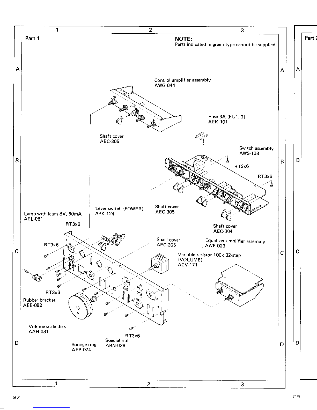
Part
1
NOTE:
Parts indicated
in
green
type cannot
be supplied.
Control
amplif ier assembly
AWG-044
Fuse
3A
(FU1,2)
AEK.1O1
Shaft
cover
AEC-305
e<r1
Switch assembly
6
Shatt cover
AEC-305
Lamp with leads 8V,
50mA
AEL.O81
RT3x6
Lever
switch
(PowER
)
ASK-124
Shaft
cover
AEC-305
Shaft cover
AEC-304
Equalizer
amplifier
assembly
AWF-023
Variable
resistor
100k
32-step
(VOLUIVlE)
ACV-171
d
cP'
RT3x6
Rubber bracket
AEB.O92
Volume scale disk
AAH.O31
Special
nut
Sponge
ring
ABN-028
AEB-074
Page 27
Inot
be
supplied.
utch
assembly
ws-l08
x6
\i
ffi
Part
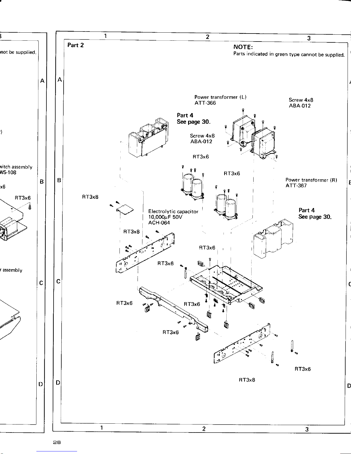
2
NOTE:
Parts
indicated
in green
type
cannot
be supplied.
Power transformer
(L)
ATT.366
Screw 4xg
ABA-OI2
Part
4
See
page
30.
Screw
4x8
ABA.O12
RT3x6
?i
/-\ i
| {l}--
tl..'l
d{=]
l
"\+
capacrtor
Power
transformer
(R)
ATT-367
RT3xB
Part
4
See
page
30.
RT3x6
1ti
a
ft
RT3x8
Page 28

€rA-E'5c'C'tr
Part
3
NOTE:
Parts
indicated
in
green
type cannot
be
supplied.
Strain relief
AEC.079
e.w
i*
AC
power
cord
ADG-OO5
Screw 3x 10
ABA-082
Jumper
plug
AKM.OO4
Screw 3x8
ABA-093
Screw
3x 10
ABA.O82
Special screw
ABA-115
Screw
3x8
AB4-093
4
Screw
for
ground
(GND)
Terminal
(SPEAKERS)
AKE.026
('
AKE.O3O
Flat washer
ABE-035
Screw
3x10
ABA.O82
%,,,,
AC socket
(AC
OUTLET)
AKP-O04
Terminal
(TAPE
2)
AKB.O35
Terminal
(TAPE
1)
AKB.O35
c\ .)
qh
Terminal
(TUNER/AUX)
AKB.036
Phono
jack
assembly
AWX.107
q'
Terminal
(PRE/POWER
AMPI
AKB.O35
A A
B
c
c
D
D
Page 29

Part
4
NOTE:
Parts
indicated in
green
type cannot be supplied.
Insulator
spacer
Transistor
AEG288
2586l7A/A/-R
or
O
/',
\t
' "o
RT3x8
Power amplif
ier assemblY
AwH-051
i1il,..,['u
q.
7]eftr,
Transistor
2SD587A/A/-R
or
O
"*ffi
lnsulator spacer
AEC-288
Transistor
socket
AKH-006
Switch
AssemblY
(Aws.108l
Phone
jack
(PHONES)
AKN-OO8
Rotary
switch
(SPEAKERS)
ASD.O54
Lever
switch
(F
ILTER)
ASK-110
Variable
resistor
{BALANCE)
ACV-112
Lever
switch
(LOUON
ESS/MUTING)
ASK-I
10
Washer
faced
nut
ABN.O24
Rotary
switch
(MODE)
ASD-053
Lever
switch
(TAPE)
ASK-I13
Screw 3x6
ABA-1
16
Special
nut
ABN-027
Washer faced nut
ABN.O24
Relay
ASR.O23
Screw
3x6
ABA.116
Special
nut
ABN.O27
Screw 3x6
ABA.,I
16
30
Page 30
ElA-8sclc,tr
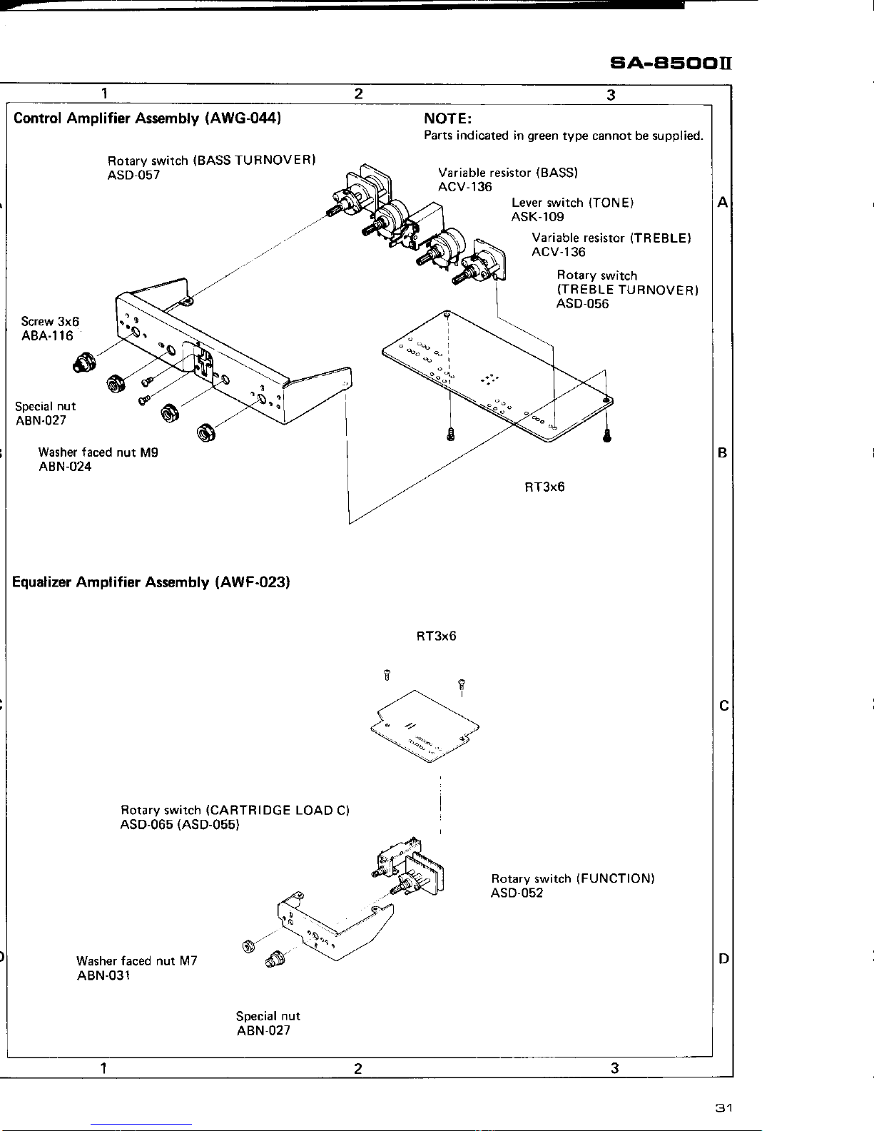
Control Amplifier Assembly
(AWG-044)
NOTE:
Parts
indicated
in
green
type cannot be supplied.
Variable resistor
(BASS)
ACV-136
Rotary
switch
(BASS
TUFNOVERI
ASD-057
Lever switch
(TON
E)
ASK-109
Variable resistor
(TR
EBLE
)
ACV-136
Rotary
switch
(TREBLE
TU RNOVE
R)
ASD-056
Screw
ABA-1
3x6
l6
s
Special
nut
ABN.O27
Washer iaced nut
Mg
ABN-024
Equalizer Amplifier
Assembly
{AWF-023}
RT3x6
Rotary switch
(CARTRIDGE
LOAD
C)
AS0,065
(ASD-055)
#,
A<iu
Rotary switch
(FUNCTION)
ASD-052
Washer
faced nut l\il7
ABN.O31
@'s
Special
nut
ABN,O27
\..A\
\5."
Page 31
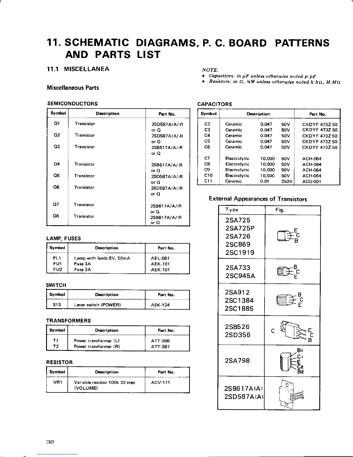
11.
SCHEMATIC
DIAGRAMS,
P.
C.
BOARD
PATTERNS
AND PARTS LIST
11.1
MISCELLANEA
NorE:
.
Copacitors:
in
UF
unless
otheruise
noted
p:pF
.
Resistors:
in a,
y.W
unless
otherwise
noted
h:ha. M:Msl
Miscellaneous Parts
SEMICONDUCTORS
CAPACITORS
Symbol
Dascliption
P6rt
No.
o1
a2
o3
o4
o5
06
o8
Transistor
Transistor
Transistor
Transistor
Transistor
Transi,tor
Transistor
Tranaistor
25D587A/A/,R
orO
25D587A/A/-R
25B6't 7AlA/,R
or Ll
25B617A/A/-R
orO
25D587Ai
A/-R
orO
2SDs87A/A/-R
orO
2SB617A/A/,R
orO
25B617A/a/-R
orQ
Symbol
Description
Part
No.
c3
c4
c5
c7
c8
c9
cl0
cl1
Ceramic
Ceramic
Ceramic
Ceramic
Ceramic
0.047 50v
o.o47
50v
o.o47 50v
o.M1
50V
0.047 50v
Eleclrolytic
10,000
5OV
Electrolytic l0,0OO
50V
Electrolytic
10,000
50V
Electrolytic 10.000
50V
Ceramic
O.01
250V
oKDYF 4732 50
CKDYF
4732
50
cKDYF 4732 50
cKDYF 4732
50
cKDYF 4732 s0
ACH-064
ACH-064
ACH-064
AC H-064
ACG-00'l
LAMP.
FUSES
S.ymbol
O6cription Pari
No.
PLl
FUl
FU2
[-amp
with
leads
8V, 50mA
Fuse
3A
AE L,081
AEK-IO1
AEK.1O1
External
Appearances
of Transistors
Type
Fi9.
25A725
2SA725P
25A726
2SC869
2SC1919
rT+-E^
tJ.Fe"
2SA733
2SC945A
a\-\
@si
2SA91
2
2SC1384
2SC
1 885
ffiXB.
v/A{
_w
2S8526
25D356
E
c
B
2SA798
#t"
2586 17A(A)
25D5874(A)
SWITCH
Syrnbol D6cription Part
No.
Lever switch
(POWERI
ASK-124
TRANSFORMERS
S],mbol O€scrip(ion Pa?t
No.
T1
'f2
Pow€r
translormqr
(L)
Povwr
translormer
(R)
ATT-367
RESISTOR
Symbol D6criplion
Pan No.
VR1 Variable rosislor
1Ook 32-slep
(VOLUME)
ACV-171
Page 32
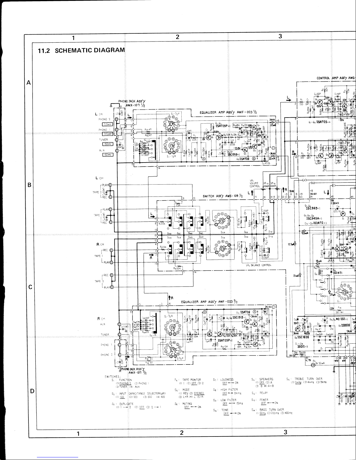
11.2
SCHEMATIC
DIAGRAM
PHoN0 JACK
ASS'/
,il4
AWx-
to1
t/2
l-'1-_'l
l.I*i
!
CoNTRoL
'Al'lP
ASS'/
AWo-
ca56P
Qr
4,".0'
2SArl25"+
-
llnu
L
I
64
L
cr
l:
PH0N0
2
i
lE".vll
PHONO
I
I
@
-a
d
'Y,,
o
,.troFffi
!
I
Ita
,:,',',,,[,'T.-..ffil:
TU
NER
frsrTill
Arj X
fEd;Nl
t
iApt r
t
-^^- ^ Q r
lAtE
/
o-i
lol
L
REC
R*t
I
REc
TAPE
]
L
cir
Lr*
roo.
[r*"
L
oru
R
cri
AJX
TUNER
t:t:
,
,t:
i:
,:
:,l
pr10N0
Phio
Nc
rPLAY
I
PLA\
-
ar
u
v7"
RLC
oi'Strrg',
0r,0+,0s
2SC945A^l
o,s
-o,rlS24'12
x:
Sso
@o:9
o
oo@
I.
VR?
BALANCE
CONTROL
r!
-
--l
EQUALTZER
Af'lP ASST
AwF
-0232/2
D-ao
ns24?l
@rn
:tA
hv/
tn
l6
Dn.Oi.llZ'250
xz
os258526
0"2
-?s,
;tll
l--
*
'1'
L
----ri-"
I-..1
--J
.n{oNoJA0K
Ass'x,
'
AWX
-10'1
12
SWITCHES;
.
S,:
FUNCTION
Sr : L0UDNESS
S,, , SPEAKERS
Srs
:
TREBTE
TURN
0VER
OFFT
ON
(l)
OFF
(2)
A
(l)
2kHs
(2)
4kHr
(3)EkHi
(3)
B
(a)
A+B
Se
:
r-llGr-i
Fll-TER
OFF.-tBKHr Sn,
RELAY
Sg
'
LOW
FILTER
56 : POWER
OFF
-:*
l5Hr
C'FF
-ON
Sro
:
TONE
,
Srn : BASS
TURN
OvER
OFFa*-gN
(i)
l00Hz
(2)2C0Hr
(3)400Hr
Sz
,
INPUT
:CAPACIIAN0E
SELECT0
R(
pF)
(
r
)
r00
(2)
200
(3)
300
(4)
400
S:
:
DUPLI OATE
S+
:
TAPE
l10NlT0R
il)
I
(2)
OFF
(3)
2
Ss
:
l10D E
(])
REV i2)
STEREO
(3)
L+R
(4)
L
(5)R
Se
:
MUTING
CFF
-*
ON
$6yR5]ssr<
R'132r
fr
VRr
VOIUIl
E
CONTROL
6
I
C)
a
E
r
<-
ci
nA
I
t*i##
iCrl00P
cs,0r
2SCl919
xz
=
_S
=
d
(3)
2-
I
Page 33

Si r AscICItr
NOTEr
'
The
indicated semiconductors
are
representative
ones
only. Other
alternative
semiconductors
may be used
and are
listed
in the
parts
I i
sts.
SwrrcH
Assy
AwS-
Ps2f2
=
n
=
a
ol;l
r
EEJ
=
AX
i
I
a,-0o
2SA'125'+
Qs-04
2SCl9l9
xc
VRr
EASS
C0NTROL
VR4
TREBLE
CONTROL
i?nu
L
I
64
oi8tars,,
0r,0+,0s
2SC945A^:
o,s
^0,,,1S24t12
x:
l{.+Y
0,lsct526
Dr'Da
3002'
a
?v
Pl'
8v
50
mA
TRIBLE
TURN
OVER
r2trHr
(2)4kHr
(3)EkHi
0z,Qr
L.-.lslrre-
l0 nA
-4?v
15nA
(
4ry
l3A)
2r-B
AC I?OV
60Hr
AC
OUTTETS
SW]TCHED
UNS$IITCHED
zOOIJ(UD
I1AX
zOOW(UL)
I1AX
IOOVA(
CSA)
t,|AX
MOVA
(CSA)
HAX
=r^
5l
!''
0,,0,
-
|
ZsosE?AtA)xz
s#frl-r---r
:-B
93Lu-4^.-
2SB6l'lA(A)
'z
V
(v)
lnA
D
I
lar
:
DC VOLTAGE
AT NO
INPUT
SiqNAL
:
DC
V0LTAGE
AT
60W
x2
0,-rTf'Uo
:
DC
CURRENT
AT,.N0
INPUT
SIGNAL
;
SIONAL
VOTTAGI
:AT
IOWX2
(IKHT)
OUTPUT
(
E
O)
RESISTORS;
iN 0Hh,l/4W,
t5oh
T0TERANCE
UNLESS
OTHERWISE
NOTED
K:KQ,
11
:MQ
CAPACITORS
,
iN.lJF
UNLESS
OTHERWISE
NOTED P
'
PF
".....-t
2SClEE5xz
I
lQq
I
I
I
I
I
lo,
I
I
zE +E.iq Y
F"
-l
lt
,uu
I
,Ta
J
-I
"T
)tl
I
20'B
lt+
,8
Qr,
er
-
rn'o
ir'
;
|| |I Ml
''.ll
'
"u,,,,1
ll =L Ii,ji i ,l
PoWER Ar,lP
AssT AwH-051
x
o
E
).
fr:
o
ca
0.6'v
o42SA9l2
D,ls24'l3
i3r+t,
o'h,?L8'i,,
%.,.r*
l0E2
F
^t=
!l=*
t9
=
a
E
et*,Q01:,,,:,,,er,s,0,01
U
d
t:
FI
=
q
6
Page 34

11.3 SWTTCH ASSEMBLY
(AWS-I081
aTAPE
1
1
;-TAPE
211
REC
PB
3
r0
REC
E
PB
LI
FROIl
TONL AMP
VRVRcT
E E
E OIJT
n
r0
13
tB232+
c2220P
L
IN 1
Y
a
(
6l
ri
F'
.
l,
Li;
R
IN
3
'-.-'-r
(A)
oo@:
c-.
)<
at:
VRz BALANCE CU\TROL
i
REc
r!
P0
LTAPE
]J
L F L i
TO
LTAPL
2.I
E
t1gXS.
Rr
AC
AC
VR
VRcr
TTRANS Lr
-8 -B
-B
-B
.
B AC
t-
Ssl
o@o
54 60
50 58
51
56 59 62 6r
s5
41
4E 4
4?V
(4W)
-
4?v
(
40v)
AC
35V
4?v
(40v)
=
_s
41v
(
Ar3sv
T
63,
si
,^T
T
i=<
-
2+4v
l2.5mA
u2
DI
({
2l mA
2+.4\
=
;,
cta
Dr
D8
U3
-----J
I-
-JF-
J;_J____,L
Ln
0.01
(
-rc 0.01
da
d
C,q
o.o r
c,i
0.01
4€.5V
rol
sv2SCt626
0r3
^,l-250
0s-
on
Drt
s3 +'l
-^45.!v
Oe
e238526
R52
4'l
D"
?*:tae
-*-1-;
5-f5;
4 Ars'A t+bt{
IUE
Z
X4
t>
i*T',.
tibtr'
to'+
lW-250
2x8
54>
TJI=< lr
=lia1'
j*5f
€
t_
Page 35

Cg
022/rO
Drs-0n
ls24'?2xl
o'u
13.6u
;0, ";t*,;_l
5
+l
o
os
2SA'?33 24'13
t50(3\,1/)
cl
tLl
a
a
a
d
ff
30
L
32
R
?3
3t
R
33V 3?rnA
p.oJ,,u
Rsr
r50(3w)
|
16.5V
;v2SC1626
0rr
_i
FRO
M
IONE AI4P
E
OUT
23
24
E
0s 25C945A
Drt,Du
I
S24'73
x2
u)^t
+
at>
c)
.tt
at!o
+5
39
AC
UNE
36 3E
33 34
tlr1-250
4
Page 36

AWG.O4
AWG.04
AWG{44
No.7
AWG{44
N0.6
AWH'051
No.23
i
,I
o!
t-l
H
t\t*,
tC"
fl
U
--o
36
n
H
t\t"
H
U
L
t-
2A
a
5
ll
3l}
olr}
AWH.O
AWH-Ol
AWH-O!
AWH{I
i
c6 1ooo0
5
i-'
".;;."
AWH-051
No.16
(L)
AWH-O51
No.16
(R)
AWH-051
No.17
(R)
REo
AWH-Osl No.l7
{L}
Page 37

BA-45C'C'tr
VOLUME AWF{23
No.16
AWFO23
No.'15
AWFO23
No.14
AurGO44
No.4
AWG+14
No.9
TAPE
1
(B)
BEC
TAPE
2
(R)
REC
TAPE
1
(L)
REC
TAPE
2
(L'
BEC
AYlrc{X4 No.3
AWF023 No.17
AWFO23 No.18
Aure-o44
No.2
No.14
lR)
1
No.20
(Rl
I No.13
(Rl
I No.21
(Rl
c,
loooo/5o
cro't
oooo/5o
arD
o.o47
AWH{s1
No.19
(R)
AWH.Osl
No.l9
(L)
AWH.O61 No.l3
(L)
AWH.O61
No.2l
(L)
AWH{,61
No.14
(Ll
AwH{51
No.2O
(L}
Page 38

Parts
List of Switch Assembly
(AWS-108)
SEMICONDUCTORS
Symbol O€scription
Part No.
o1
a2
o3
o4
o5
o6
a7
oa
o9
D1
o2
D3
D4
D5
D7
D8
D9
D't
0
Dl1
Transistor
Transistor
Transistor
Transi!tor
Transistor
Transistor
Transistor
Transirtor
Transistor
Diode
Diode
Diode
Diode
Diode
Diode
Daode
Diode
2SC869-D
or C
2SC869-D
or C
25C945A-O or
25C945A-O
orR
2SA733-O or R
l2SA823-O
or R)
2SC945A-O or
2SC1384-0
or
25Cl626-0
or
(2SD381-N4
or
R
R
L)
258526-C
or D
(2SA816'0
or
Y)
30D2
(GP-25D)
{ERC01,02)
30D2
(GP-25D)
{ERC01-02}
30D2
(GP-25D)
{
ERC0't,021
30D2
(GP-25D)
(ERCO1-02)
30D2
(GP-25D)
(ERC01-02)
30D2
(GP-25D)
{ERC01-O2)
30D2
(GP-25D1
(ERC01,02)
30D2
(GP,25D)
(
ERCOl
-02)
10E2
{s180't,02)
(1
S 1 886)
10E2
(srB01-02t
(1S1886)
10E2
{stB01-o2)
(151886)
Symbol
Descriplion
D12
D13
D14
D15
D16
Dl1
D18
Dr9
D20
D21
Diode
Zener diode
Ze^e(
diode
Diode
Diode
Diode
Diode
Diode
Diode
10E2
(srB01-o2)
(1S1886)
w2,250
\
lz-250
152412
(1S1554)
152472
(1S
1
554)
'ts2412
(ls1554]
152473
(1S1555)
1S2473
{
1S
1555}
152471
'ts2413
(1S1555)
SWITCHES
Symbol
Description
P6rt No.
s3
S4
S5
s6
s7
s8
s9
s11
Lever switch
(OUPLICATE)
Lever switch
(MONITOR)
Rotary
switch
(MODE)
Lever
swilch
(MIJTlNGl
Lever
switch
(LOUDN
ESS)
Lever
swatch
(HIGH
FILTER)
Lever
swatch
(LOW
F ILTER)
Rotary
switch
{SPEAKERS}
ASK.113
ASK-113
ASD-053
ASK-110
ASK,110
ASK-11O
ASK-110
ASD-054
ASR-023
RESISTORS
Symbol
D€scription
R1
R2
R3
R4
R5
R6
R7
R8
R9
R10
R11
R12
R13
Carbon film
2.2k
Carbon film
2.2k
Carbon film
2.2k
Carbon film
2.2k
Carbon
falm
3.3k
Carbon film
3.3k
Carbon
film
41k
Carbon film
47k
Carbon
{ilm
5.6k
Carbon film
5.6k
Carbon film
5.1k
Carbon
film
5.1k
Carbon film
2.2k
RD%PS
222J
RD%PS
222J
RD%PS
222J
RD%PS 222.J
RD%PS
332J
RD%PS
332J
RDY.PS 473J
RD7.PS
473J
RD7.PS
562J
RD7.PS
562J
RD7.PS 512J
RDY.PS 5,I2J
RD%PS
222J
39
Page 39

Symbol Description
R14
Rl5
R16
R17
R18
R19
R20
R21
R22
R23
R24
R25
R26
R27
R28
R29
R30
R31
R32
R33
R34
R37
R38
R39
R40
R41
442
R43
R44
R45
R46
R47
R48
R49
R50
R51
R52
R53
R54
VR2
Caroon f ilm
2.2k
C€rbon
film
22Ok
Carbon film
22Ok
Carbon
film
33k
Carbon film
33k
Carbon film 15k
Carbon
film
15k
Carbon film
47k
Carbon
film
47k
Carbon film
2k
Carbon
film
2k
C€rbon film
82
Carbon
film
82
Carbon lilm
16k
Carbon film 16k
Carbon film 18Ok
Carbon
film
18k
Carbon
film
51k
Carbon film
2.7k
Carbon
film
2.7k
Carbon film
27k
Carbon film
6.2k
Carbon film
43k
Carbon film
1O0
Metal oxide
27O
Metal
oxide
390
Carbon
film
15k
13k
11k
10k
10k
10k
Carbon film
C€rbon film
C€rbon
film
Carbon
film
Carbon tilm
Carbon
film
Carbon tilm
Carbon film
Metal
oxide 150
Carbon
film
47
Carbon
film
47
Metal oxide
620
Variable resistor 250k-HB
IEALANCE}
10k %w
4.7k %W
4.7k
%W
680
2W
150
3W
3W
2W
RD%PS 222J
RD%PS 224J
RD%PS 224J
RD7.PS
333J
RD%PS
333J
RDy.PS
1 53J
RD7.PS 153J
RD7.PS 473J
RD7.PS 473J
RDY.PS 2O2J
RD%PS
2O2J
RDY.PS 82OJ
RD7.PS
82OJ
RD7.PS 1
63J
RD%PS 163J
RDZPS
1 84J
RD'/.PS 1
83J
RDi/.PS 513J
RD%PS
272J
RD/.PS 272J
RD%PS 273J
RD7.PS
622J
RDY.PS
433J
RDY.PS
101J
RSl P 271J
RS'I P
391J
RD7.PS 153J
RD%PS 133J
RD%PS 1 13J
RD%PS 1 O3J
RD%PS
1O3J
RD%PS 1
O3J
RD%PS
1 O3J
RDY,PS
412J
RD%PS 472J
R52P
681J
RS3P 151J
RS3P
151J
RD%PSF
47OJ
RD%PSF
47OJ
R52P
62,I
J
ACV 172
Symbol
Dsscription Part No.
c6
c7
c8
c9
c10
c11
c12
c13
c14
c17
c18
c19
c20
c21
c22
c23
c24
Electrolytic
Electrolytic
Electrolytic
Electrolytic
Electrolytic
Electrolytic
Electrolytic
Ceramic
Ceramic
0.0056 50v
0.68
35V
0.68
35V
o.22 10V
o.22 10V
410
6V
100 16V
2.2 50V
0.01
150v
o.01
150v
100
35V
220 50V
220 50V
0.01 125V
Ceramic 0.01
15OV
Ceramic
0.01
150V
Ceramic
0.001
50V
Ceramic O.O01 50V
Electrolytic 100
35V
Electrolytic
Electrolytic
Electrolytic
Ceramic
coMA 562J 50
cszA
R68M
35
cszA
R68M
35
CSSA R22M IO
cssA R22M 10
cEA 471P 6
cEA 101P 16
ACH-317
ACG-004
ACG-004
ACG-004
ACG-004
CKDYF 1022 50
CKDYF 1022 50
cEA
101P
35
cEA
101P
35
cEA 22tP 50
cEA221P 50
ACG-003
OTH ERS
Symbol Descriplaon
Part
No.
Phone
iack
{PHON
ESI
Fuse clip
Washer faced nut M9
Special
nut
AKN.OOS
AKR.O3O
ABN,O24
ABN.O27
CAPACITORS
Symbol
Description
Part No.
c1
c2
c3
c4
c5
Ceramic 22Op sov
Ceramic 22Op 50V
Mylar
O.12 50V
Mylar
O.12 50V
Mylar
0.0056 50V
ccDsL 221K 50
ccDsL
221K 50
coMA r 24K 50
coMA 124K 50
COlr'lA 562J
50
40
Page 40
11.4 PHONO
JACK ASSEMBLY
(AWX-I07I
aA-95ClCttr
Parts List of Phono Jack Assembly
(AWX-107)
Phon o I
L
Phono
1
R
2
F.
3
4
5
6
F.
,]
Symbol D.acriplion Part
No.
cl
c2
Coramic capaciror 0.(X7 50V
Csramic capacitor
0.(X7 sOV
T.rminal
{PHONO
1, 2)
oKDYF 4732 50
cKDYF 4732 50
AKB.O27
Page 41

1T.5
EOUALIZER
AMPLIFIER ASSEMBLY
(AWF.O23)
3
65
tF
o3
ii";;i;"
a.|15=S
J2
to
(a
l-
@o
@
\@
/@
--t
._l
69
(9
-.i
o-oo
C:r
4
il'
Rr
?,10k
-,
?.1il(
R
.1'r
k
t)
Crs 41/35
R84lk
t
;
t'
')
8.,
4 t {l/6
B
c5
0 021
r- "2?0P
1,,"
4100P
12
A
B
c
D
A
B
c
D
Page 42

aA-a5C'Clu
Foil
side
AWS-I08
No.7
AUX
(L)
c2 o.o47
Fl
D'
TUNE R
(L'
AWX-107
No.2
Page 43
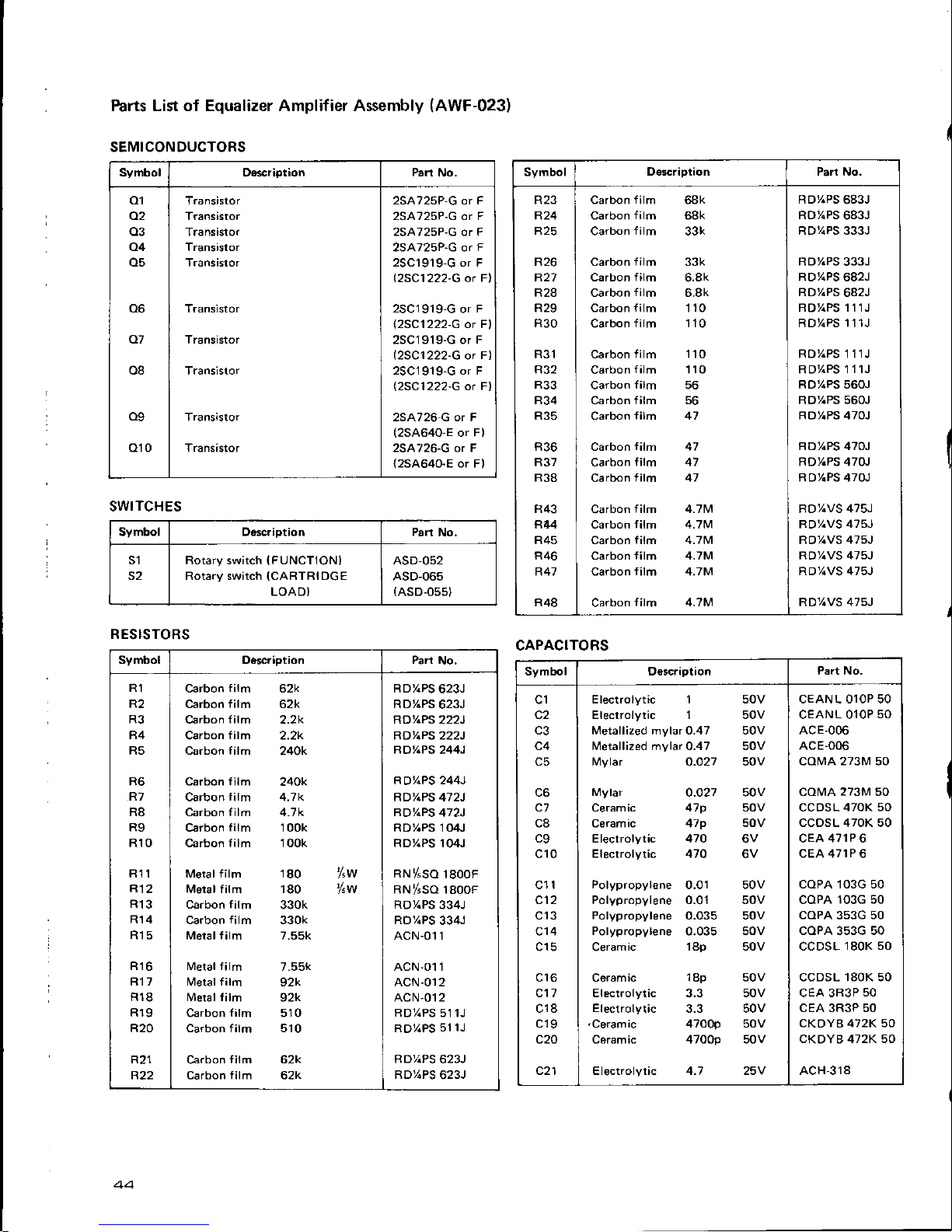
Parts List of Equalizer Amplif ier Assembly
(AWF-023)
SEMICONDUCTORS
Symbol D€scription
Part
No.
o1
a2
o4
o6
a7
08
09
010
Transistor
Transistor
Transistor
Transistor
Transistor
Transistor
Transistor
Transistor
Transistor
2SA725P'G
or
F
2SA725P-G or F
2SA725P'G or F
25A72sP-G or
F
2SC1919-G or F
12sC1222-G
ot
Fl
2SC1919-G
or
F
\25C1222-G
ot Fl
2SC1919-G or F
125C1222-G
ot
Fl
2SC1919-G or F
125C1222-G
ot Fl
25A726 G or F
(2SA64O-E
or F)
2SA726-G
or F
I2SA64OE
or F)
SWITCHES
Symbol Doscription Part
No.
s2
Rotary switch
{FUNCTION)
Rotary switch
(CARTRIDG
E
LOAD}
ASD,052
ASD-065
{ASD,055}
I
Symbol
Description
R26
R27
R28
R29
R30
R31
R32
R33
R34
R35
R24
R25
R36
R37
R38
R43
R't4
R45
R46
R47
R48
Carbon
film
68k
Carbon
film
68k
Carbon
film
33k
Carbon
film
33k
Carbon film
6.8k
Carbon
film
6.8k
Carbon tilm 110
Carbon
film 110
Carbon
tilm 110
Carbon
film
110
Carbon
{ilm
56
Carbon film 56
Carbon
film
47
Carbon
film
47
Carbon
film 41
Carbon
tilm 47
Carbon
film 4.7M
Carbon film 4.7M
Carbon film 4.7M
Carbon
lilm
4.1M
Carbon
Iilm
4.7M
Carbon
lilm 4.7M
RDt/.PS
683J
RD7.PS
683J
RD7.PS 333J
RDl.PS
333J
RD%PS 682J
RD7.PS
682J
RD7.PS
111J
RDz.PS 111J
RD7.PS 1 11J
RD7.PS11IJ
RD/.PS 56OJ
RD%PS 56OJ
RD/.PS 47OJ
RD7.PS 47OJ
RD/.PS 47OJ
RDY.PS 47OJ
RD%VS 475J
RD%VS
475J
RDy.VS
475J
RD7.VS 475J
RD7.VS 475J
RD%VS 475J
RESISTORS
Symbol Description Part
No,
R1
R2
R4
R5
R6
R8
R9
R10
Rl1
R12
R13
R14
R15
R16
R17
R18
R19
R20
R21
Carbon
film
62k
Carbon
film
62k
Carbon
film
2.2k
Carbon
film
2.2k
Carbon Iilm
240k
Carbon lilm
240k
Carbon
film
4.1k
Carbon lilm 4.7k
Carbon
film
100k
Carbon Iilm 1Ook
Metal film 180
f'W
Metal film 180
l,w
Carbon film
330k
Carbon
film
330k
Metallilm 7.55k
Metal film
7.55k
Metal film
92k
Metal lilm
92k
Carbon
lilm
510
Carbon film 510
Carbon
Iilm 62k
C€rbon film 62k
RD/.PS
623J
RD7.PS
623J
aD%PS 222J
RD%PS 222J
RD%PS
244J
RD%PS 244J
RD%PS 472J
RD%PS
472J
RD7.PS
'l
OiU
RD7.PS 1
O4J
RN%so
rSooF
RN,lso
18ooF
RD%PS
334J
RD7.PS
334J
ACN-011
ACN,O11
ACN-012
ACN,012
RD%PS
511J
RD%PS
51lJ
RDY4PS
623J
RDY PS
623J
CAPACITORS
Symbol Oescription
Part No.
c1
c2
c3
c5
c6
c7
c8
c10
c11
c12
c13
cl4
c15
c17
c18
c19
c20
c21
Electrolytic 1 50V
Electrolytic 1 50V
Metallized mylar O.47 50V
lvletallized mylar 0.47 50v
Mylar O.O27 50V
Mylar
O.O27 50V
Ceramic 41p 50V
Ceramic 41p
50V
Electrolytic 47O
6V
Efectrolytic 47O
6V
Polypropyl€ne
0.01
Polypropylene 0.0't
Polypropylene
0.O35
Polypropylene
0.035
Ceramic
1ap
Ceramic
18p
Electrolytic 3.3
Electrolytic
3.3
,Ceramic
4700p
Ceramic 4700p
50v
50v
50v
50v
50v
50v
50v
50v
50v
50v
Electrolytic 4.7 25V
CEANL OlOP 50
CEANL OlOP
50
ACE,006
AC E-006
coMA
273t\/l 50
coMA
273M
50
ccDsL
470K 50
ccDsl 470K 50
CEA 4?1P 6
cEA 471P 6
coPA 103G 50
coPA
103G 50
coPA
353G
50
coPA 353G 50
ccDsL
180K 50
ccDsL 180K 50
CEA 3R3P
50
CEA 3R3P 50
cKDYE
472K 50
CKDYB 472K 50
ACH-318
Page 44
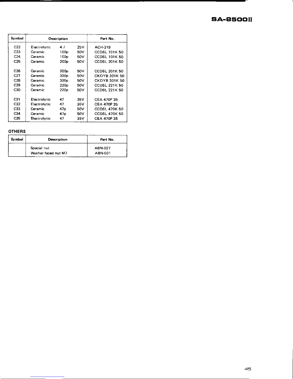
Symbol
D63cription
c26
c27
c2a
c29
c3o
c22
c23
c24
c31
c32
c33
c34
Electrolytic 4.1
25v
Ceramic 100p
sOV
Ceramic 100p
50V
Ceramic 200p
50V
Ceramic 200p
50V
Ceramic 30Op sOV
Ceramic
300p 50V
Ceramic 22Op sOV
Ceramic
220p 50V
Electrolytic 47
35V
Electrolytic
47
35V
Ceramic 47p
50V
Coramic 47p
50V
Efectrolytic
47 35V
ACH-318
ccDSL 101K
50
ccDSL 101K 50
ccDsL 201K 50
ccDsl 201K 50
CKDYB
3O'I K 50
CKDYB
3O'I
K 50
ccDsL 221K
50
ccDsl 221K 50
cEA 470P
35
cEA 470P 35
ccDsL 470K 50
ccDsL 470K 50
cEA 470P
35
sA-a5C'cltr
OTHERS
Symbol D6scription Part
No.
Special nut
Washer laced nut
M7
A8N-027
ABN-O31
45
Page 45

A
c
D
A
c
D
I
I
;
11.6
CONTROL
AMPLIFIER ASSEMBLY
(AWG-o.T4)
3E
3s
(o
Nt
a9
R4
2201(
I
;
3
fir
8.2(
=
a
R
iu
2 2/50
x1
a6
00?
C,S
0
0?
Cro
0062
22i(
R25 lf4
6BK
,l-
:-,
!tJ
4't t1 4'l
r.rl
\ltl
l6
i.
Cso l00r
25
t00
/.
!
Page 46

sA-45ClCltr
Foil
side
AWS-I08
No.62
AWS-I@
No.64
AWS-1G
No.20
'l0g
No.21
Page 47

Parts List of Control Amplifier
Assembly
(AWG-044)
SEMICONDUCTORS
t
Symbol
Oetcription
Part No.
o1
a2
o3
a4
o6
o7
o8
Transistor
Transistor
Transistor
Transistor
Transistor
Transistor
Transistor
Transistor
2SA725'G
or F
(25A640.E
or Fl
2SA725-G or F
(25A640-E
or
F)
2SA725-G
or F
(25A640-E
or Fl
2SA725-G or F
(2SA640-E
or F)
2SC1919-G or
F
(2sC1222-E
ot Ul
2SC1919-G or F
12sc1222-E
ot
Ul
2sC1919-G
or F
12sc1222-E
ot Ul
2sC1919-G
or F
l.25C1222-E
or U)
SWITCHS
Symbol
I
Descriprron
I
Pan No.
Sl0 I
Lever swrrch
(TONE)
I
aSK-109
514 | Rotarv swilch
(BASS
TURNOVERI ASD-057
S15 | Rotary switch
ASD-056
{TR
EB LE TURNOVER}
f:
I
{
RESISTORS
Symbol
D6cription
Part No.
R1
R4
R5
R6
R7
R8
R9
R10
Rl1
R12
R13
R14
R15
Rl7
R18
R19
R20
Carbon
film 22O
Carbon
film 22O
Carbon
lilm 22Ok
Carbon
film
22Ok
Carbon
lilm 1Ook
Carbon
lilm 100k
Carbon
film
8.2k
Carbon film a.2k
Carbon film 1k
Carbon
lilm 1k
Carbon
film 10k
Carbon film 10k
Carbon
film
68k
Carbon
film
68k
Carbon
film 7.5k
Carbon
film 7.5k
Carbon
film 56
Carbon
Iilm
56
Carbon
film 100k
Carbon film 1Ook
RD%PS 221J
RD%PS 221J
RD1/.PS 224J
RD%PS 224J
RD7.PS 1O4J
R D'I.PS
't
O4J
RD7.PS 822J
RO%PS 822J
RD7.PS 1O2J
RDI.PS 1
O2J
RDy.PS 1 O3J
RD7.PS 1O3J
RD7.PS 683J
RD74PS 683J
RD%PS
'T52J
RD/.PS 752J
RO%PS 560J
RD'I.PS 560J
RD7.PS 1 O4J
RD%PS 1
O4J
Symbol
Dsscription
Part
No.
R22
R23
R24
R25
R27
R2a
R29
R30
R31
R32
R33
R34
R35
R37
R3a
R39
R40
R41
R42
R43
R44
R45
R46
R47
R4a
R49
R50
R51
R52
R53
R54
R55
R56
R57
R58
R59
R60
VR3
1M
1M
1M
,IM
1M
1
rvl
1
rvl
12k
12k
22k
22k
6.8k
6.8k
100
100
Carbon
film 22k
Carbon
film 22k
Carbon
Iilm 6.8k
Carbon
film 6.8k
Carbon
tilm 1M
Carbon
film
Carbon film
Carbon
film
Carbon
film
Carbon
film
Carbon
film
Carbon
film
Carbon
film
Carbon
film
Carbon
film
Carbon film
Carbon film
Carbon film
Carbon
film
Carbon film
RD'/.PS 223J
RD%PS 223J
RD%PS 682J
RD%PS 682J
RD7.PS
1OsJ
RD%PS 1 OsJ
RDY.PS I
OsJ
RD%PS 1OsJ
RD%PS
1OsJ
RD%PS 1O5J
RDi/.PS't05J
RD7.PS 1OsJ
RD/.PS 123J
RD%PS
123J
RD7.PS 223J
P.D%PS 223J
RD74PS 682J
RD%PS 682J
RD7.PS
101J
RD7.PS 101J
RD%PS 475J
RD%PS 475J
RDY4PS 475J
RD%PS 475J
R D'I.PS 1 A4J N L
RD7.PS 184J NL
RD%PS IO4J NL
RDy.PS'IO4J NL
RD7.PS
332J
RD7.PS
332J
RD7.PS 1 O3J
RD%PS 1 O3J
RDI.PS 1
O4J
RDz.PS 1 O4J
RD'/.PS 1 02J
RD7.PS 1 O2J
R D 7.PS 1
O2J
RD%PS 1O2J
RD7.PS
1O2J
RD%PS 1 O2J
Carbon
film
Carbon
film
Carbon
tilm
Carbon
film
Carbon
film
Carbon
Iilm
Carbon
film
Carbon film
Carbon
film
Carbon
film
Carbon
tilm
Carbon
film
Carbon
film
Carbon
film
Carbon
film
180k
100k
100k
3.3k
3.3k
10k
10k
100k
100k
lk
1k
1k
1k
,IK
1k
Carbon
film 4.7M
Carbon
film 4.1M
Carbon film 4.7M
C€rbon
film 4.7M
Carbon film 180k
variable resistor'lOok-B
(BASS)
|
ACV 136
Variable resistor 100k-B
(TREBLE)
ACV-I36
4B
Page 48
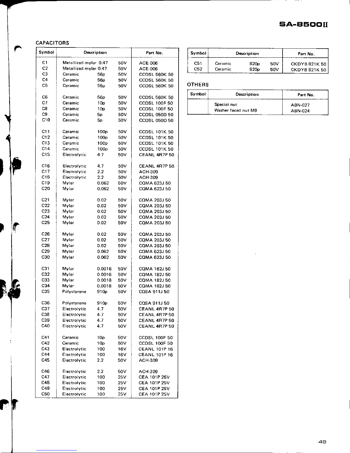
CAPACITORS
Symbol O€scription
Part
No.
c1
c2
c4
c5
c6
c1
c8
c9
cl0
cl1
c12
c13
c15
cl6
c17
c18
c19
c20
c21
c22
c23
c24
c25
c26
c27
c2a
c29
c30
c31
c32
c33
c34
c35
c41
c42
c43
c44
c45
c36
c37
c38
c39
c40
c4'7
c48
c49
c50
Metallized
mylar 0.47
Metallized
mylar O.47
Ceramic
56p
Ceramic 56p
Ceramic
56p
50v
50v
50v
50v
50v
Ceramic
Ceramic
Ceramic
Ceramic
Ceramic
Ceramic
Ceramic
Ceramic
Ceramic
Electrolytic
Electrolytic
Electrolytic
Electrolytic
Electrolytic
Ceramic
Ceramic
Electrolytic
Electrolytic
Electrolytic
Electrolytic
Electrolytic
Electrolytic
Electrolytic
Electrolytic
100p
sOV
1O0p
50V
l00p
50V
'I00p
50V
4.7
50V
56p
1op
10p
5p
5p
0.02
o.o2
o.o2
o.o2
D.O2
50v
50v
50v
50v
50v
Electrolytic
4.7
Electrolytic
2.2
Electroiytic
2.2
Mylar
0.062
N.4ylar
0.062
50v
5ov
50v
50v
50v
50v
50v
50v
50v
50v
o.o2 50v
o.o2 50v
0.02 50v
0.062 50v
0.062 sov
o.0016 50v
0.0016 50v
0.0018 50v
0.0014 50v
910p 50V
910p 50V
4.7 50V
4.t
50v
4.1
50V
4.7
50V
1op
1op
100
100
2.2
2.2
100
100
100
100
50v
50v
16V
't6v
50v
50v
25V
25V
25V
AC E
006
ACE-006
ccDsl
560K 50
ccDsl 560K
50
ccDSL 560K 50
ccDsl 560K 50
ccDsl 100F 50
ccDsl 1ooF 50
ccDSL O50D 50
ccDsL 050D 50
ccDsL r01K
50
ccDsL 101
K 50
ccDsl 101K 50
ccDsL
'101K
50
CEAN L 4R7P 50
CEANL 4R7P 50
ACH-309
ACH-309
cor\rA 623J 50
coMA
623J 50
coMA 203J
50
coMA 203J 50
coMA 203J 50
COI\i1A
203J
50
coMA 203J 50
coMA
203J 50
coMA
203J 50
coMA 203J
50
coMA
623J 50
coMA 623J 50
coMA 162J
50
coMA 162J 50
coMA 182J 50
coMA
182J
50
cosA
911J 50
cosA
91lJ
50
CEAN L 4R7P
50
CEANL 4R7P
50
CEAN L 4R7P 50
CEAN L 4R7P 50
ccDsl
100F
50
ccDsL 100F
50
CEANL 101P I6
CEANL
1O1P 16
AC
H
-309
ACH,3
09
CEA 101P 25V
CEA 101P 25V
CEA 101P 25V
CEA
101P 25V
siA-a5c'Cltr
I
cs2
|
Ceramic
820p
SoV
I
CKpyB 821K
So
I
OTH ERS
@---il.-_-]
I
Washer faced
nut Mg
]
ABN-024
I
F
49
Page 49

11.7 POWER
AMpLtFtER
ASSEMBLY
(AWH-051)
25058?A,,2
2SB6l?A,2
r--T,-----
I
I
c-
c*
1
J
=
t-
=
(a)
o=
l0mA
Rrz
150
Dr
,1s24'13 R,o
6Bx
5
(1/lw),a
0,p
2SA198
_
,
D410E2
rls33K
R4
33h
i.
I
E
u1
R6
2.1X
r
\f
+
c!
Rre
05(2W)
=
rrdire
Rr3
160
=
::'
t.
06
258528
E
c-
c-
+
jsp
zSCl88S'Z
R
22
2.'1K
c.
Rr4
150
o/1v/)
a042SA9l2
cro
0
04?
8.2v
,1'^
..
o_
c3
4?P
l<t2
l00P
-ji
R,lrox
A
c
A
B
c
D
A
4
,
$
I
Page 50

gA.BEOC'II
AWS-lm No.48
lll
AWS.IG
No.57
(Rl
c!
(Lt
c,o
(B)
l OOOO/5O
POWER AMP
IN
Awsloa
No.47
(Ll
AWS1oA
No.68 {R}
c,
{L)
ce
(R)
10000/50
AWS-|08
No.4O
Atlrs-lS
No.41
Aws-16
No.s'l
(Ll
AWS-16
No.52(Rl
AWS-108
No.44
lLl
AWS.lOg No.rE
(R)
Page 51

hrts List of Power Amplif
ier Assembly
(AWH-051
)
SEMICONDUCTORS
Symbol Description
P.rt
No.
o1
a2
o3
04
06
D1
D2
D3
o4
Transistor
Transistor
Transistor
Transistor
Transistor
Transistor
Diode
Diode
Diode
2SA79A-G or F
2SC1885-5 or R
(2SC1903-V
or
2SC1885-5
or R
(2SC1903-V
or
2SA912-R
or S
{2SA898-B
or V)
25D358-D or
C
258528-D or
C
152473
(1S1555)
152473
{
1S1555}
STV.3H
10E2
(srB01-01)
{1S1885)
CAPACITORS
Symbol
Deso
ipiion
Part
No,
c1
c2
c3
c5
c7
c8
c9
c10
c11
c12
cl3
Metallized mylar 0.68 100V
Ceramic 10Op 50V
Ceramic 41p 50V
Efectrolytic
22 35V
Electrolytic 330 6V
Ceramic |5p 5O0V
Ceramic 15p 50V
Ceramic 22Op
500V
Ceramic 22Op 5O0V
Ceramac O.Mi 50V
Ceramic O.O47 15OV
Ceramic 0.01
150V
Electrolytic 1 50V
ACE-010
ccDsL 101K 50
ccDsL 470K 50
cEA 220P
35
cEA 331P 6
ccDsL
150K
500
ccDsL 150K 50
ccDsL 221K 500
ccDsL 221K 500
cKDYF 4732 50
ACG-009
ACG-001
CEANL OlOP 50
OTH ER
Symbol Description
Part No.
LI AF choke coil 2.2!H T63,009
RESISTORS
Symbol
D6cription
P6rt No.
VR1
R1
R2
R3
R4
R6
R8
R9
R10
R11
Rl2
R13
R14
R15
R16
R'l7
R18
R19
R20
R21
R22
R23
R24
R25
Sema-fixed 1O0-B
Carbon
film
330k
Carbon film
2.2k
Carbon
film
62k
Carbon lilm
39k
Carbon tilm
3.3k
Carbon lilm
2.7k
Carbon film
2.7k
Carbon film
62k
Carbon
film
6.8k
Carbsn film
Carbon
film
Carbon
film
Carbon
film
C€rbon
film
Metal film
Metal film
Metal
film
Metal
film
Metal film
Metal film
Carbon film
Carbon
filrn
Metal
oxide
M€tal
oxide
68
160
160
150
150
0.5
0.5
0.5
0.5
4.1
%w
2vtl
vN
Z,ltl
2V,l
4.7
'lW
2.1k
2.1k
10 2W
10
lW
ACP-O19
RD7.PS
334J
RD%PS 222J
RD%PS
623J
RD%PS
393J
RD7.PS
332J
RD%PS
212J
RD%PS 272J
RD%PS 2'12J
RD/.PS
623J
RD%PS
682J
RD%PS
68OJ
RD'/.PSF
161J
RDT.PSF
161J
RD%PSF
I51J
RD%PSF
151J
RN2H
OR5K
RN2H
OR5K
RN2H
OR5K
RN2H
OR5K
RN1 H 4R7K
RN 1H 4R7K
RO%PS
272J
RD%PS
272J
RS2P 100.1
RSl P 100.1
5e
Page 52

12.
PACKING
sA-C'5Clcltr
Vinyl pouch
AHG.O23
Connection
cord
AOF-125
Reinforced
cardboard
AHC.035
Packing
case
AHD-430
Side
pad
AHA.130
Vinyl bag
E11
Operating
instructions
AR
8.205
Sheet
cover
AHG-057
'
Side
pad
AHA-1
NI.l
T
i----
Page 53

 Loading...