

Page 1
DVD RECORDER
PRV-9000
THIS MANUAL IS APPLICABLE TO THE FOLLOWING MODEL(S) AND TYPE(S).
Type
KU/CA AC120V 1
Model
PRV-9000
Power Requirement Region No. Remarks
ORDER NO.
RRV2563
¶ This service manual should be used together with the following manual(s):
Model No. Order No. Remarks
DVR-7000/KU/CA RRV2536 DVD Recorder for Consumer model
DVR-A03/KB RRV2423 DVD-R/RW Drive Unit
CONTENTS
1. CONTRAST OF MISCELLANEOUS PARTS
2. SCHEMATIC DIAGRAM
3. PCB CONNECTION DIAGRAM
4. PANEL FACILITIES AND SPECIFICATIONS
PIONEER CORPORATION 4-1, Meguro 1-chome, Meguro-ku, Tokyo 153-8654, Japan
PIONEER ELECTRONICS (USA) INC. P.O. Box 1760, Long Beach, CA 90801-1760, U.S.A.
PIONEER EUROPE NV Haven 1087, Keetberglaan 1, 9120 Melsele, Belgium
PIONEER ELECTRONICS ASIACENTRE PTE. LTD. 253 Alexandra Road, #04-01, Singapore 159936
PIONEER CORPORATION 2001
.......................................
..........................
........
.......
2
6
18
25
T – ZZK NOV. 2001 Printed in Japan
Page 2
PRV-9000
1. CONTRAST OF MISCELLANEOUS PARTS
NOTES:
Parts marked by "NSP" are generally unavailable because they are not in our Master Spare Parts List.
The mark found on some component parts indicates the importance of the safety factor of the part.
Therefore, when replacing, be sure to use parts of identical designation.
Screws adjacent to mark on product are used for disassembly.
Reference Nos. indicate the pages and Nos. in the service manual for the base model.
When ordering resistors, first convert resistance values into code form as shown in the following examples.
Ex.1 When there are 2 effective digits (any digit apart from 0), such as 560 ohm and 47k ohm (tolerance is shown by J=5%,
and K=10%).
560
47k
0.5
1
56 x 10
47 x 103
R50
1R0
1
561
473
RD1/4PU J
RD1/4PU J
RN2H K
RS1P K
561
473
R50
1R0
Ex.2 When there are 3 effective digits (such as in high precision metal film resistors).
5.62k RN1/4PC F562 x 10
CONTRAST T ABLE
1
5621
5621
PRV-9000/KU/CA and DVR-7000/KU/CA are constructed the same except for the f ollo wing :
Part No.
Ref. No. Mark Symbol and Description DVR-7000 PRV-9000 Remarks
/KU/CA /KU/CA
PCB ASSEMBLIES
P7- 1 TUMJ ASSY VWV1885 DWX2201
P7- 2 REAR JACK ASSY VWV1887 DWX2203
P7- 3 3D Y/C ASSY VWV1888 DWX2204
P7- 4 FRONT JACK ASSY VWV1886 DWX2202
P7- 6 POWER SUPPLY ASSY VWR1347 DWR1354
P5- 1 RF Antenna Cable VDE1025 Not used
P5- 2 Stereo Audio Cable VDE1033 Not used
P5- 3 Video Cable VDE1034 Not used
P5- 6 NSP Warranty Card ARY1026 DRY1197
P5- 7 Operating Instructions (English) VRB1275 DRB1313
P5-11 NSP DVD-RW Disc Ver 1.1 VZZ1001 Not used
P5-15 Packing Case VHG2122 DHG2169
P7-33 Rear Panel VNA2328 DNC1591
P7-34 Bonnet VXX2814 DXX2507
P7-41 Insulator VXA2424 DXA1920
P7-42 DVD Badge VAM1119 DAM1084
P7-46 Tray Panel VNK4801 DAX1012
P7-51 Screw VBA1082 BBZ30P060FZK
P7-56 Screw FBT40P080FNI FBT40P080FZK
P9- 7 Front Aluminium VAH1392 DAX1009
P9- 8 PIONEER Badge VAM1124 BAM1004
P9-12 Input Sheet VEC2199 DEC2449
P9-17 Panel Base VNK4983 DAX1010
P9-18 Input Door VNK4924 DAX1011
P9-19 Dial Knob VNK4802 DAC2017
P9-20 Power Button VNK4803 DAC2016
P9-21 Play Button VNK4804 DAC2015
Notes : The numbers in the remarks column correspond to the numbers on the “ EXPLODED VIEWS ”.
For PCB ASSEMBLIES, Refer to “CONTRAST OF PCB ASSEMBLIES”, “PCB PAR TS LIST”, “2. SCHEMATIC DIAGRAM” and
“3. PCB CONNECTION DIAGRAM”.
TUJB ASSY VWM2103 DWM2134
PACKING SECTION
EXTERIOR SECTION
Screw BBZ30P060FMC IBZ30P080FCC No. 1
Screw BBZ30P060FMC BBZ30P060FZK No. 2
Ground T erminal Not used DKE-102 No . 3
NSP History Label Not used VRW-348 No. 4
FRONT PANEL SECTION
2
Page 3
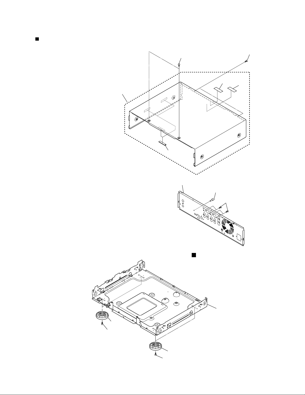
EXPLODED VIEWS
PRV-9000
Bonnet (DXX2507)*1
*1 Case of service parts :
Gasket of three pieces, 65 Label
and History Label have already
been attached to Bonnet.
Screw (BBZ30P060FZK)
2
65 Label
4
Gasket
Rear Panel
3
Insulator
1
Screw (BPZ30P080FZK)*2
*2 Please pay attention when assembles
REAR JACK ASSY.
B
At first please do temporary assembly of
four screw to fix S terminal.
Please assemble it tight next.
Screw of an other side does not
assembled when does not do temporary
assembly.
Chassis
Insulator
1
3
Page 4
PRV-9000
CONTRAST OF PCB ASSEMBLIES
TUMJ ASSY
A
F
DWX2201 and VWV1885 are constructed the same except for the following :
Mark Symbol and Description
R1009, R1044 RS1/16S0R0J RS1/16S102J
R1070–R1073 Not used RS1/16S101J
R4150, R4151 Not used RS1/16S0R0J
3D Y/C ASSY
C
F
VWV1885 DWX2201
Although DWX2204 and VWV1888 are different in part number, they have the same service parts.
FRONT JACK ASSY
D
F
DWX2202 and VWV1886 are constructed the same except for the following :
Mark Symbol and Description
F2050 CHIP BEAD Not used DTF1070
VWV1886 DWX2202
Part No.
Part No.
Remarks
Remarks
PCB PARTS LIST
Mark No. Description Part No.
REAR JACK ASSY
B
F
SEMICONDUCTORS
Q1502 2SA1576A
Q1501, Q1503-Q1505 2SD2114K
D1520-D1523 UDZS5.6B
RESISTORS
R1501, R1503, R1505, R1519, R1520 RS1/16S75R0F
R1535 RS1/16S75R0F
Other Resistors RS1/16S&&&J
OTHERS
JA1532, JA1534, JA1536, JA1538 DKB1049
JA1531, JA1535 Y/C CONNECTOR DKB1050
JA1533, JA1537 BNC CONECTOR DKB1051
JA1530 BNC CONECTOR 3P DKB1052
CN1501, CN1502 VKN1392
POWER SUPPLY ASSY
I
F
2P PIN JACK
B TO B CONNECTOR 24P
SEMICONDUCTORS
IC271,IC301 VZF1089
IC801,IC910 VZF1107
Q252,Q272,Q410,Q911 2SC1740
Q312 2SC2655
Q313 DTC114ES
Q314 DTC143ES
Q120 VZF1101
Q110 VZF1108
Q211 VZF1109
Q221 VZF1110
Mark No. Description Part No.
Q251 VZF1111
Q271,Q910 VZF1112
Q412 VZF1113
Q111,Q122,Q131,Q501 VZF1114
Q311 VZF1115
D134,D220,D311,D424 10ELS2
D112,D122,D252,D453 1SS270A
D211 MTZJ39D
D103 UK1V26
D212 VZF1045
D611 VZF1051
D210,D410 VZF1053
D612 VZF1057
D101 VZF1063
D901 VZF1075
D701 VZF1081
D451,D452 VZF1083
D251,D801 VZF1087
D510,D511 VZF1088
D127 VZF1100
D110,D123 VZF1105
D222,D224 VZF1118
D421-D423 VZF1119
TH451 THYRISTOR VZF1117
PC101-PC103,PC501 VZF1116
PHOTO COUPLE
RESISTORS
R410 FUSE RESISTOR (47Ω) VZC1063
R212 FUSE RESISTOR (10Ω) VZC1065
OTHERS
P221,P226 FUSE (1A) VEK1041
P610 FUSE (0.75A) VEK1042
P252,P611 FUSE (1.5A) VEK1048
P271,P701,P915 FUSE (2.5A) VEK1056
P815 FUSE (3.5A) VEK1073
FU101 FUSE (3.15A) VEK1044
4
Page 5
1
Model name/destination
2
Version of the recorder software
3
Revision No. of the system control computer software
4
Version No. of the tuner microcomputer, result of confirmation on combination between the tuner microcomputer and the
system control computer
5
Information on the built-in drive (Name of the manufacturer, model name of unit into which the drive is built, version No., CPU
model name, serial No., result of confirmation of combination with the system control computer
6
Version No. of AV1
7
Region No.
OK: Correct combination
NG+: Version of the tuner microcomputer too high
NG-: Version of the tuner microcomputer is too old
OK: Correct combination
NG+: Version of the drive too high
NG-: Version of the drive is too old
OK: Serial No. of the drive is Registered
NG: Serial No. of the drive is not Registered
1
DVR-7000 /KU
2
SYSCON : RELEASE_1 1 2
3
R e v : 1. 6 1 0 9. 2.
2 2 6. 2. 4
4
TUFLCON : 1. 5 2 0 0
OK
5
DRIVE : PIONEER
DVD–RW DVR–7 0 0 0
1. 6 1 C 7 9 1 1
OK
A E T 0 0 0 0 2 2 4 J P
OK
DEVICE : AV1=ES6. 0
6
REGION : 1
$
Description of Each Mode
1. Mode Menu 1 [Version information, etc.]
Subscreen 1
NOTE
Firmware using for PRV-9000 is the same as DVR-7000.
Therefore, model name of debugging screen is displayed with DVR-7000.
This is not product failure.
Show an example as follows.
PRV-9000
5
Page 6
1
PRV-9000
2. SCHEMATIC DIAGRAM
2.1 OVERALL WIRING DIAGRAM
A
SW ASSY
H
(VWG2315)
F
FL ASSY
(VWG2314)
B
23
FRONT JACK ASSY
D
F
(DWX2202)
3D Y/C ASSY
C
F
TERMINAL
A
A
F
TUMJ ASSY (DWX2201)
1/4F-4/4F
(DWX2204)
4
JOG ASSY
G
(VWG2316)
C
RECORDER DRIVE
MAIN
(DWX2148)
This service manual
does not include
this recorder section.
Refer to the S/M for
DVR-A03(RRV2423).
AXM7014
E
E
MAIN ASSY (VWV1894)
1/10-10/10
D
6
1234
Page 7
5
Note : When ordering service parts, be sure to refer to "EXPLODED VIEWS and PARTS LIST" or "PCB PARTS LIST"
678
PRV-9000
A
B
C
REAR JACK ASSY
B
F
(DWX2203)
POWER SUPPLY ASSY
I
F
(DWR1354)
D
7
5
6
7
8
Page 8
1
PRV-9000
23
4
2.2 TUMJ (1/4) and REAR JACK ASSYS
8
(Comp)
(S-Y)
CN7001
7
Q1102
2SA1576A(QR)
3
1
2
A
(C-Y)
(Cr)
(Cb)
TUMJ ASSY (DWX2201)
1/4F
3
1
2
Q1103
2SA1576A(QR)
Keyed Clamp
E 7/10
A
A
3/4F
B
A
3/4F
(S-C)
(S-Y)
Output Filter
Y-Progre.
Q1201
2SA1576A(QR)
Y-Interlace
Q1203
2SA1576A(QR)
Cb-Progre.
Q1205
2SA1576A(QR)
Cb-Interlace
Q1207
2SA1576A(QR)
Cr-Progre.
Q1209
2SA1576A(QR)
6
Cr-Interlace
Q1211
2SA1576A(QR)
Q1108
DTA124EUA
(S-Y)
(S-C)
Q1105
A
3/4A3/4F
DTA124EUA
C
A
3/4F
(S-C)
(S-C)
(S-C)
(S-Y)
(S-Y)
Q1106
2SA1576A(QR)
(S-Y)(Comp)
3
(S-C)
E2
C2
1
E
B2
B
C
3
2
(S-Y)(Comp)
(S-Y)
(S-Y)
2
4
D
A
2/4F
Q1172
DTC124EUA
V/U(Comp)
(Comp)
1
(Comp)
(Comp)
(Comp)
(Comp)
A
4/4F
8
A
1/4F
1234
Page 9

18
(C-Y)
5
678
PRV-9000
(Comp)
: COMPOSITE VIDEO SIGNAL ROUTE
(S-Y)
: S–Y VIDEO SIGNAL ROUTE
(S-C)
A
2/4F
(C-Y)
(Cr)
(Cr)
(D)
(D)
16
: S–C VIDEO SIGNAL ROUTE
(C-Y)
: COMPONENT Y SIGNAL ROUTE
17
(Cb)
(Cb)
(Cb)
(Cr)
(C-Y)
Cr Level Adj.
2SC4081(QR)
2
Q1411
1
3
2
1
3
Q1311
2SC4081(QR)
19
(D)
21
(C-Y)
(Cb)
(Cr)
REAR JACK ASSY
B
F
(DWX2203)
(Cb)
(Cr)
(C-Y)
(Cb)
: COMPONENT Cb SIGNAL ROUTE
(Cr)
: COMPONENT Cr SIGNAL ROUTE
(D)
: DIGITAL AUDIO SIGNAL ROUTE
: AUDIO SIGNAL ROUTE(L ch)
A
Component Y Level Adj. Cb Level Adj.
DTC124EUA
Q1333
Q1341
DTC124EUA
25
26
22
24
23
20
(Comp)
(S-Y)
(S-C)
2SD2114K(VW)
3
2
1
(S-Y)
(S-C)
Q1504
2
1
3
3
1
2
Q1505
2SD2114K(VW)
2SD2114K(VW)
Q1501
2
1
3
3
1
2
Q1503
2SD2114K(VW)
Q1502
2SA1576A(QR)
B
(Comp)
C
(S-Y)
(S-C)
(Comp)
D
1/4F
A
5
6
7
B
8
F
9
Page 10

1
PRV-9000
2.3 TUMJ ASSY (2/4)
A
for DATA Loading
23
4
TUMJ ASSY (DWX2201)
2/4F
Q2024
DTC124EUA
C
E
A
Q2022
2SD2114K(VW)
Q2021
E
DTA124EUA
B
C
B
C
B
C
B
E
E
Q2023
2SC4081(QR)
B
to FANto FAN
2
Q2009
2SD2114K(VW)
1
3
Tuner Control U-com
C
2
Q2010
2SD2114K(VW)
1
3
CN1202
F
D
A
1/4F,3/4F,4/4F
Reset IC
10
A
2/4F
1234
EEPROM
Page 11

Q2012
HN1K03FU
5
678
PRV-9000
Q2004
2SD1664K(PQR)
2
3
1
Q2003
DTC143EUA
Q2001
Q2007
2SD1664(PQR)
DTA124EUA
2
3
1
(D)
Q2006
2SB1132(QRS)
2
3
1
Q2005
DTC143EUA
: DIGITAL AUDIO SIGNAL ROUTE
A
CN202
I F
B
Q2008
HN1K03FU
Q2016 HN1K03FU
Q2013
DTC124EUA
Q2015
HN1K03FU
A
1/4F
C
CN2001
(D)
E 2/10
Real Time Clock
: The power supply is shown with the marked box.
5
6
D
2/4F
A
7
8
11
Page 12

1
PRV-9000
2.4 TUMJ (3/4) and 3D Y/C ASSYS
A
A
3/4F
TUMJ ASSY (DWX2201)
A
4/4F
14
CN8001
15
(S-C)
23
4
Q3305
HN1K03FU-TBB
E 8/10
B
C
12
13
(S-Y)
2
3
2SC4081(QR)
1
Q3222
S-In through/
Composite
Selector
via 3D Y/C
Antiareasing Filter
(C)
(Y)
Q3223
DTC124EUA
(Y)3D
(C)3D
3D Y/C
data setting
communication
(Y)3D
(C)3D
(Comp)
3
2
EDORAM(4M)
3D Y/C Input
Level Adj.
(S-Y)
(S-C)
A
1/4F
D
12
A
3/4F
1234
(Comp)
Page 13

C
1
Q3002
2SA1576A(QR)
5
3D Y/C ASSY (DWX2204)
F
3
2
1
678
PRV-9000
A
(Comp)
: COMPOSITE VIDEO SIGNAL ROUTE
(S-Y)
: S–Y VIDEO SIGNAL ROUTE
(S-C)
: S–C VIDEO SIGNAL ROUTE
(Y)
: Y VIDEO SIGNAL ROUTE(3D Out-Y or S-Y)
(C)
: C VIDEO SIGNAL ROUTE(3D Out-C or S-C)
: AUDIO SIGNAL ROUTE(L ch)
B
(C)3D
(Y)3D
(Comp)
3D Y/C IC
1
2
Q3001
2SC4081(QR)
3
C
D
3/4F
A
5
6
7
C
8
F
13
Page 14

1
23
PRV-9000
2.5 TUMJ (4/4) and FRONT JACK ASSYS
4
A
A
TUMJ ASSY (DWX2201)
4/4F
VHF/UHF TUNER
Q4102
2SC4081(QR)
3
1
Q4107
HN1K03FU
2
(MPX)
1
(Comp)V/U
2SA1576A(QR)
3
Q4105
2
E2
Q4111
C2
HN1A01FU(YGR)
B
B2
B
E
Q4110
C
2SA1576A(QR)
E
C
Q4111
HN1A01FU(YGR)
Terrestrial Video
Level Adj.
B
B2
C
Q4112
HN1C01FU(YGR)
E
C2
Q4112
HN1C01FU(YGR)
E2
(Comp)V/U
B
Q4411
3
2SB1132(QRS)
Q4412
DTC143EUA
Q5001
RN1903
C
E
Q5001
RN1903
B
C2
B2
E2
1
Q4401
2
2SD1664(PQR)
2
3
1
Q5003
RN1903
C
E
Q5003
RN1903
B
C2
B2
E2
C
C
Q5005
B
RN1903
C2
E
B2
Q5005
E2
RN1903
EEPROM
D
14
A
4/4F
1234
Page 15

5
678
PRV-9000
Audio Multiplex
Decoder IC
Q4301
2SD1664K(PQR)
2
3
1
V/U
Q4601 HN1K03FU
FRONT JACK ASSY
D
F
(DWX2202)
(Comp)
(S-Y)
(S-C)
V/U
E 9/10
CN9001
(S-Y)
(S-C)
(Comp)
DV TERMINAL
A
B
RN1903
B
5
C
Q4201
E
B2
C2
E2
Q4202
RN1903
Audio Selector
A
(Comp)
: COMPOSITE VIDEO SIGNAL ROUTE
(S-Y)
: S–Y VIDEO SIGNAL ROUTE
(S-C)
: S–C VIDEO SIGNAL ROUTE
: AUDIO SIGNAL ROUTE(L ch)
A
A
A
A
3/4F
3/4F
2/4F
1/4F
1/4F
C
D
: The power supply is shown with the marked box.
4/4F
A
6
7
D
8
F
15
Page 16

1
PRV-9000
2.6 POWER SUPPLY ASSY
23
4
A
B
POWER SUPPLY ASSY (DWR1354)
I
F
STANDBY
STANDBY
STANDBY
C
STANDBY
CN101
AC
IN
D
16
I
LIVE
NEUTRAL
F
1234
Page 17

5
678
PRV-9000
A
CN201
E 2/10
CN2003
B
CN202
CN203
CN204
A 2/4F
CN2001
C
R-DRIVE
MAIN
CN406
NOTE OF SPARE PARTS IN POWER SUPPLY (SYPS) UNIT
• In case of repairing, use the described parts only to prevent an accident.
• Please write the red mark on the board when the primary section of POWER SUPPLY (SYPS) Unit is repaired.
• Please take care to keep the space, not touching other parts when replacing the parts.
5
6
7
I
8
F
CN1201
F
D
17
Page 18

1
23
PRV-9000
3. PCB CONNECTION DIAGRAM
3.1 TUMJ ASSY
A
F
D
CN2002CN1202
B
4
F
(DNP2016-A)
TUMJ ASSY
A
F
SIDE A
E
CN2001
E
CN8001
C
NOTE FOR PCB DIAGRAMS :
1. Part numbers in PCB diagrams match those in the schematic
diagrams.
2. A comparison between the main parts of PCB and schematic
diagrams is shown below.
Symbol In PCB
Diagrams
BCE
BCE
D
D
Symbol In Schematic
Diagrams
BCEBCE
BCE
DGGSS
BCE
DGS
Part Name
Transistor
Transistor
with resistor
Field effect
transistor
Resistor array
3. The parts mounted on this PCB include all necessary parts for
several destinations.
For further information for respective destinations, be sure to
check with the schematic diagram.
4. View point of PCB diagrams.
Connector
Capacitor
SIDE A
P.C.Board
Chip Part
SIDE B
CN7001
E
FAN
MOTOR
FAN
MOTOR
18
3-terminal
regulator
I
CN202
A
F
1234
Page 19

5
678
PRV-9000
VR4101
CN3501
C F
Q2008
IC2005
Q2012
IC3241
Q3221
Q3224
Q4401
Q5001
Q5003
IC5001
IC2001
IC2003
Q2014
IC2010
Q4304
IC2002
Q4302
IC4302
Q4303
IC2008
IC2007
IC2004
IC2012
Q2001
Q2003
IC2006
IC2009
Q2013
Q1221
IC3421
Q4107
Q4104
Q5005
IC5501
IC2017
Q2021
Q2024
IC4202
Q4201
Q4301
Q4202
Q4103
Q1102
Q1103
Q1112
Q4404
Q2005
Q2007
Q2016
Q2015
Q4411
Q4412
Q1222
Q4102
Q4601
IC4601
Q1113
Q1115
IC1171
IC1102
IC1101
Q1105
Q1108
Q1101
Q1106
A
B
01
Q1411
IC1004
Q1224
Q1221
Q1226
Q1228
Q1230
Q1232
IC1312
IC2011
IC1421
IC1002
IC1003
IC1051
C
D
Q1225
Q1227
Q1229
Q1231
Q2004
Q1341
IC1311
IC1351
VR1311
VR1313
B FB F
Q1330
Q1335
Q1337
Q1340
Q2010
Q2009
CN1501 CN1502
F
19
A
5
6
7
8
Page 20

1
PRV-9000
23
4
A
B
Q4112
Q4111
Q4110
Q4105
IC4302
Q4304
IC4201
Q8001
Q1172
Q2002
Q1201
Q1203
Q1205
C
D
Q1207
Q1209
Q1211
Q1342
IC2013
20
A
F
1234
Page 21

5
678
PRV-9000
A
B
(DNP2016-A)
SIDE B
TUMJ ASSY
A F
C
D
F
21
A
5
6
7
8
Page 22

1
23
PRV-9000
3.2 REAR JACK, 3D Y/C and FRONT JACK ASSYS
4
A
REAR JACK ASSY
B
F
FRONT JACK ASSY
D
F
CN2003
A F
CN1001CN1002
A FA F
B
CN9001
E
(DNP2016-A)
C
3D Y/C ASSY
C
F
A
F
22
CN3002
Q3305
B
CFD
F
1234
F
IC3302
D
(DNP2016-A)
Q3304 Q3001IC3301
SIDE A
VR3301
IC3201
(DNP2016-A)
IC3001
IC3101
Page 23

1
234
PRV-9000
FRONT JACK ASSY
D
F
(DNP2016-A)
Q1505
Q1503
Q1504
Q1502
Q1501
REAR JACK ASSY
B
F
A
B
3D Y/C ASSY
C
F
1
Q3002 Q3301Q3302
SIDE B
2
(DNP2016-A)
(DNP2016-A)
F
23
BFC
F
3
D
4
C
D
Page 24

1
PRV-9000
3.3 POWER SUPPLY ASSY
POWER SUPPLY ASSY
I
F
A
B
23
LIVE NEUTRAL
4
Q1111
Q120
Q110
Q131
Q122
IC301
Q252
IC801
C
Q410
Q412
Q311
Q501
Q312
Q272
IC271
Q313
Q314
Q910
Q251
Q271
Q211
IC910
Q911
Q221
D
SIDE A
EF
CN2003
24
CN1201
CN2001 R-DRIVE
A F
MAIN
I
F
1234
CN406
Page 25

AC IN
Y
P
B
P
R
COMPONENT
AUDIO AUDIO
DIGITAL OUT
VHF UHF
CONTROL
OUT
IN
SIGNAL GND
S-VIDEO S-VIDEO
VIDEO VIDEO
OUTPUT
INPUT
12 12
/
VIDEO OUT
L
R
L
R
AUTO
REC
OPTICAL
COAXIAL IN
OUT
1 6
13
14
2 7 8 105 9
12 11
3
4
4. PANEL FACILITIES AND SPECIFICATIONS
4.1 PANEL FACILITIES
Rear panel
PRV-9000
1 AC IN – Power inlet
2 COMPONENT VIDEO OUT (BNC jacks)
For connecting to a TV or monitor that has component
video input
3 VIDEO OUTPUT 1 (S-Video jack)
For connecting to a TV, monitor, AV receiver or other
equipment with S-Video input
4 VIDEO OUTPUT 2 (BNC jack)
For connecting to a TV, monitor, AV receiver or other
equipment with a composite (standard) video input
5 VIDEO INPUT 1 (S-Video jack)
For recording from a camcorder, VCR or other equipment with S-Video output
6 VIDEO INPUT 2/AUTO REC*1 (BNC jack)
For recording from a camcorder, VCR or other equipment with a composite (standard) video output
7 DIGITAL OUT OPTICAL
For connecting to an AV receiver, Dolby Digital/DTS
decoder or other equipment with optical digital input
8 DIGITAL OUT COAXIAL (RCA Pin jack)
For connecting to an AV receiver, Dolby Digital/DTS
decoder or other equipment with coaxial digital input
9 SIGNAL GND terminal
This terminal is the SIGNAL GND terminal. Under
certain environmental conditions which create a lot of
noise, may fail to operate. The SIGNAL GND terminal
is provided in such a case that the ground (GND)
connections are linked among the devices used. It is
not a safe grounding terminal.
10 VHF/UHF IN (F-type jack)
Connect the TV antenna here
11 VHF/UHF OUT (F-type jack)
Passes the signal from the VHF/UHF IN to your TV/
monitor
12 CONTROL IN / OUT (monaural mini jacks)
Use for connecting to other Pioneer components
bearing the Pioneer Î mark. Connect the CONTROL
OUT of one component to the CONTROL IN of another
using a mini-plug cord. The device at the beginning of
the chain acts as the remote control sensor for everything in the chain.
13 AUDIO INPUT 1, 2/A UTO REC*1 (RCA Pin jacks)
For recording from a camcorder, VCR, satellite receiver
or other equipment
14 AUDIO OUTPUT 1, 2 (RCA Pin jacks)
For connecting to the audio inputs of a TV, monitor, AV
receiver or other equipment
*1Auto Recording works by detecting a signal at the VIDEO
INPUT 2 jack. Auto Recording will not work if there is only
an audio signal with no video signal.
25
Page 26

PRV-9000
4.2 SPECIFICATIONS
General
System .................................DVD-Video, DVD-R/RW, Video-CD, CD
Power requirements.................................................. 120 V, 50/60 Hz
Power consumption ....................................................................65 W
Power consumption in standby mode ............................ 2 W (FL o f f )
Weight ....................................................................................... 7.0 kg
Dimensions .................................... 420 (W) x 108 (H) x 377 (D) mm
Operating temperature................................................ +5°C to +35°C
Operating humidity.............................. 5% to 85 % (no condensation)
TV forma t .................................................................................. NTSC
Recording
Recording format ..............................................DVD VideoRecording
DVD-VIDEO
Recordable discs ................................................ DVD-ReRecordable
DVD-Recordable
Video recording format
Sampling frequency ............................................................. 13.5MHz
Compression format ................................................................ MPEG
Audio recording format
Sampling frequency .................................................................. 48kHz
Compression format ..............................Dolby Digital or Linear PCM
(uncompressed)
Recording time
DVD-RW (VR mode)
Standard (SP) ....................................................... Approx. 2 hours
Manual rate (MN).............................................. Approx. 1–6 hours
DVD-R/RW (Video mode)
V1 ............................................................................ Approx. 1 hour
V2 .......................................................................... Approx. 2 hours
Tuner
Receivable channels
VHF ......................................................................................... 2–13ch
UHF ....................................................................................... 14–69ch
CATV ................................................................................C2–C125ch
Timer
Programs ............................................................ 1 month/8 programs
Clock ......................................... Quartz lock (12-hour digital display)
Power off memory................................................... Approx. 48 hours
Input/Output
VHF/UHF antenna input/output terminal...................... VHF/UHF set
75 Ω (F-shape connector)
Video input ...................................................... Input 2 (rear), 3 (front)
Input level.................................................................. 1 Vp-p (75 Ω)
Jack (Input 2) ................................................................... BNC jack
Jack (Input 3) ................................................................... RCA jack
Video output .......................................................................... Output 2
Output level............................................................... 1 Vp-p (75 Ω)
Jack (Ouput 2) .................................................................BNC jack
S-Video input .................................................. Input 1 (rear), 3 (front)
Y (luminance) - Input level........................................ 1 Vp-p (75 Ω)
C (color) - Input level .........................................265 mVp-p (75 Ω)
Jacks ........................................................................ 4 pin mini DIN
S-Video output ...................................................................... Output 1
Y (luminance) - Output level..................................... 1 Vp-p (75 Ω)
C (color) - Output level ......................................265 mVp-p (75 Ω)
Jack (Ouput 1) .........................................................4 pin mini DIN
Component video output
Output level........................................................ Y: 1.0 Vp-p (75 Ω)
PB, PR: 0.7 Vp-p (75 Ω)
Jacks .............................................................................. BNC ja cks
Audio input ............................................Input 1,2 (rear), 3 (front) L/R
Input level
During audio input ............................................................. 2 V rms
(Input impedence: more than 22 kΩ)
Jacks .............................................................................. RCA ja cks
Audio outpu t ................................................................ Output 1,2 L/R
During audio output ........................................................... 2 V rms
(Output impedence: less than 1.5 kΩ)
Jacks .............................................................................. RCA ja cks
Control input/output ..................................................Mini jack 1 each
DV input/output ........................... 4 pi n (i.LINK/IEEE 1394 standard)
Supplied accessories
Remote c on t r ol .................................................................................. 1
Dry cell batteries (AA/R6P) .............................................................. 2
Power cable....................................................................................... 1
Operating Instructions ...................................................................... 1
Warranty car d .................................................................................... 1
Resetting the recorder
If you need to, you can reset the recorder to all its
factory settings.
1 Make sure that the recorder is on.
2 Press and hold 7 STOP and press
The recorder turns off with all settings reset.
ACCESSORIES
Remote Control
STANDBY
OPEN
/ON
/CLOSE
CHP
NAVI
SETUP
PLAYLIST
MARK
MARK
ERASE
EDIT
DISCNAVI
(VXX2763)
ENTER
JOG MODE
PAUSE CM SKIP RETURN
CM
26
REC PLAY STOP
PREV NEXT CHANNEL
REC
PlusCode
MODE
PROGRAM
REPEAT ANGLE
TV
INPUT SELECT
TV VOLUME AUDIO SUBTITLE
TV CHANNEL MENU
SEARCH
MODE
654
A-B
SHIFT DISPLAY
S
INPUT
SELECT
CLEAR
C321
0987
TOP MENU
Dry cell Batteries
(R6P,AA)
Note: The specifications and design of this product are
subject to change without notice, due to improvement.
STANDBY/ON.
AC power cord
(ADG7021)
 Loading...