

Page 1
6th
Product Training
Guide
Generation Plasma
Models
Technical Training Department
1925 E. Dominguez Street
Long Beach, CA 90810
Page 2

Page 3

Contents
Plasma Model List…………………………4 PCB Locations………………………..…29
G5 And G6 System Comparison………..5 Operation Status Panel LED’s………..30
Overall Block Diagram………………….6~7 Power Down LED (Red Flashing)….....31
HD Digital Assembly Block……………..8 Power Down Defective Points…...…32~33
Y – Drive Block………………………...….9 3 Times Power Down Flashing……....34
X – Drive Block……………………….…..10 8 Times Power Down Flashing……....35
Differences – G5 & G6 Drive…….....11~13 Shutdown Block (Blue Flashing)…....36
X & Y Board Differences – G5 & G6….14 Audio Board Caution……………….….37
Power Supply Map – X & Y Drive…..…15 Operation Without Media Receiver…..38
Scan A & B Block…………………….….16 Power On With No Panel Drive……….39
Scan IC – 43 Inch Models……………18~19 Adjustments……………………….….40~46
Scan IC – 50 Inch Models…………...20~21 How To Clear The History……………..47
Address Circuit Blocks – G6…….…22~25 Panel Factory Mode……………….….48~56
Audio Assembly …………………..…26~27 Disassembly…………………………...57~60
Power Supply Unit…………………..….28 RS232 Connection………………..……61
Page 4
PLASMA MODEL LIS
T
y
4
Consumer Models
G6
Regular Model
Elite Model
Type Model #
43" System PDP4360HD
43" System
50" System
50" System
43" System
50" System
PDP4361HD
PDP5060HD
PDP5061HD
PRO930HD
PRO1130HD
Media
receiver
PDPR06U PDP436PU PDPS37LR PDKTS10
PDPR06U PDP436PU PDPS37LR PDKTS11
PDPR06U PDP506PU PDPS38LR PDKTS10
PDPR06U PDP506PU PDPS38LR PDKTS10
PROR06U
PROR06U
Plasma
Speakers
Displa
PRO436PU PDPS35LR
PRO506PU PDPS36LR
Table top
stand
PDK1013
PDK1013
Page 5
L
G5 & G6 System Diagram
PD
PD
PD
PD
AND ci
it
PD
Discrimination
PDPDPD
PD
Diff
Main Devi
Protecti
by models
( Power Down )
LOGIC singal
Video / Audio signal
C
t
Vid
l
R
PDPDPD
PD
PDPDPD
PD
AND
PD判別
PDPDPD
PD
5
G6 HD MODEL
SCAN Y DRIVE HD DIGITA
TEMP
SENSOR
IC3301
FLASH ROM
rcu
Power Supply
IC3156
EEPROM
V RST
V OFFSET V SUS
ADRES ADRES ADRES ADRES
LVDS
RECEIVER
LVDS
RECEIVER
LED IR
IC3401
SEQUENCE
PROCESSOR
CPU
IC3001
DVI Receiver
IC5201
MODULE
Ucom
BUFF
IC3157
DAC
LVDS
RECEIVER
HD AUDIO
IC3753
VOLUME
IC3754
BACK UP
EEPROM
IC3751
AMP
X DRIVE
LVDS
RECEIVER
erent Assy
ommon use Assy
o all of models
ce
on circuit lineSerial communication line
eo sequnce signa
G4/G5 HD MODEL
ADRES ADRES ADRES ADRES
LVDS
RECEIVER
LVDS
RECEIVER
TEMP SENSO
LVDS
RECEIVER
SCAN Y DRIVE DIGITAL PS X DRIVE
FLASH ROM
EEPROM
SEQUENCE
PROCESSOR
V OFFSET V SUS
ADRES ADRES ADRES ADRES
LVDS
RECEIVER
LVDS
RECEIVER
CPU
DAC
MODULE
Ucom
LVDS
RECEIVER
LVDS
RECEIVER
LVDS
RECEIVER
BACKUP
KEYSCAN
DVI Receiver
LED KEY IR
PANEL I/F HD AUDIO
EEPROM
BUFF
VOLUME AMP
Page 6
50 SCAN B ASSY
6
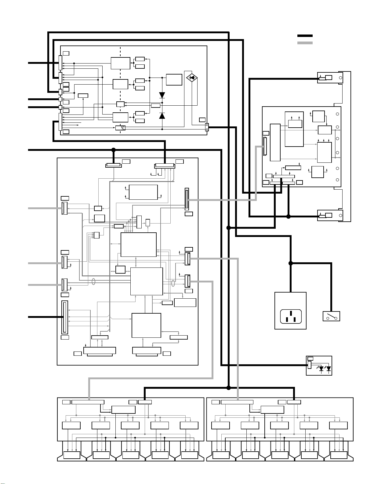
OVERALL BLOCK DIAGRAM
(UPPER)
Scan Signal
VH
IC2801
IC5V
Scan IC
PSUS
PSUS
IC5V
VH
Scan Signal
SB1
SA1
IC2802
Scan IC
IC2803
Scan IC
IC2804
Scan IC
IC2805
Scan IC
IC2806
Scan IC
CN2802
CN2702
IC2701
Scan IC
IC2702
Scan IC
IC2703
Scan IC
IC2704
Scan IC
IC2705
Scan IC
IC2706
Scan IC
Serial Data
50 SCAN A ASSY
(LOWER)
50 Y DRIVE ASSY
PSUS
PSUS
VH
IC5V
IC5V
VH VSUS
VH DC/DC Conv.
Vprst
Vprst Reg.
+5V +16.5V
VSUS
IC2252
Mask
Mod.
VSUS
+5V
+16.5V
IC2253
Mask
Mod.
IC5V
IC5V
Photo Coupler
VF
Block
SUSOUT
Soft-D
Block
IC5V/VF
VH
Y2
Y3
Vprst
+5V
Regulator
Resonance
Block
+5V
IC2101
DK Mod.
+16.5V
DC/DC
Conv.
Scan Signal
+ Reset
Block
VOFS
VSUS
+6.5V
+16.5V
+16.5V
+16.5V
+5V
VOFS
DC/DC
Conv.
Y4
+5V
Logic
Block
VOFS
Offset
Block
+16.5V
Drive Signal
+5V
60V
Y6
Y1
Y5
HD AUDIO ASSY
+16.5V
A2
+16.5V
+16.5V
IC3751
Power Amp IC
R_OUT +
R_OUT –
L_OUT +
L_OUT –
Left
Right
SP TERMINAL
IC3752
Regulator
Buffer
WOW + Volume IC
DC Detect
Block
+3.3V
A3
+9.0V
+9.0V
IC3753
IC3754
EEP ROM
+3.3V
A_Mute
A_STBY_B
R_Audio
L_Audio
A_NG_B
+9.0V
SCL
SDA
SDA
SCL
A1
HD IR ASSY
IR Receive unit
STB3.3V
U1681
AD1 AD2
Resonance
IC1555
Driver IC
V+8V
Block
V+ADR5
RE1
CN1501
AN/P BN/P
CN/P DN/P CLKN/P
Resonance
Driver IC
Block
V+ADR4
IC1554
V+3V
IC1501
LVDS Receiver
Resonance
Block
V+ADR3
IC1553
Driver IC
CLK/LE/HBLK/LBLK
CN1502
V+5V
(PEE002A-K) (PEE002A-K)
R/G/B
50 ADDRESS
V+60V
ASSY
Resonance
Block
V+ADR2
IC1552
Driver IC
Resonance
Driver IC
Block
V+ADR1
IC1551
SPEAKERS
V+8V
Block
V+ADR5
IC1555
Driver IC
CN1501
AN/P BN/P
CN/P DN/P CLKN/P
Resonance
Driver IC
Block
V+ADR4
IC1554
V+3V
IC1501
LVDS Receiver
Resonance
Block
V+ADR3
IC1553
Driver IC
CLK/LE/HBLK/LBLK
AD1 AD2
Resonance
CN1502
R/G/B
50 ADDRESS
V+60VV+5V
ASSY
Resonance
Block
V+ADR2
IC1552
Driver IC
Resonance
Block
V+ADR1
IC1551
Driver IC
Page 7
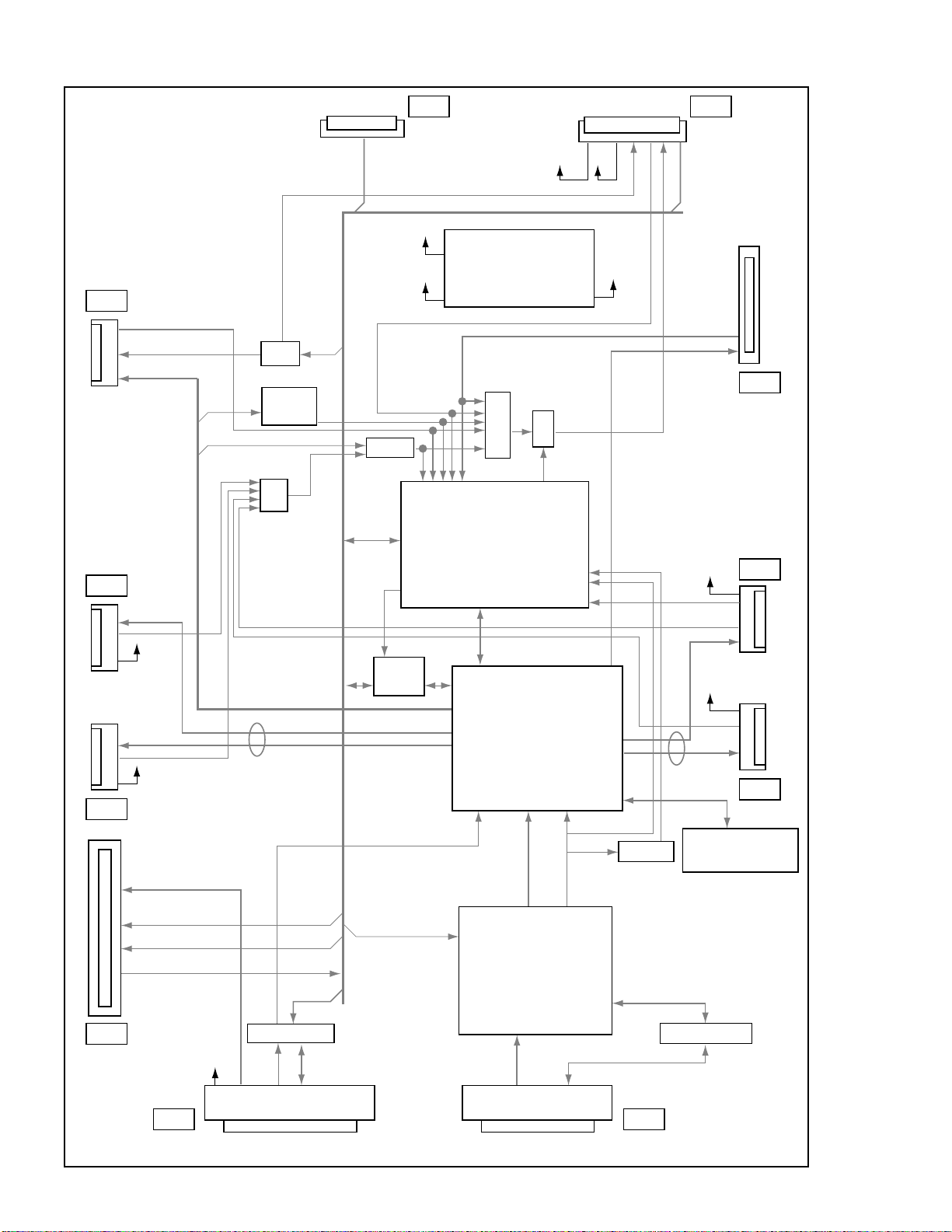
P1
7
P2
P7
+60V
P6
P5
RELAY
+16.5V
VSUS_ADJ
STA3.3V
SECONDARY PRIMARY
VSUS
+16.5V
+6.5V
VSUS_CONT
IC202
+8V
PS_PD
EXT_PD
P4
LED_R
LED_B
REM
SCAN_PD
YDRIVE_PD
YSUSTN_PD
YDD_CNV_PD
D10
SCN5V_PD
Vofs_ADJ,VYPRST_ADJ
SCAN
YSUS
DAC
Pulse
Width
OR
SCL,
SCA
ADR_PD1
D5
V+8V
V+8V
LVDS
D6
AUDIO L
AUDIO R
SCL, SDA
A_MUTE,A_STBY_B
A_NG
V+3V STB
Bus Buffer
REM
STB_MT
D3
D2 D1
HD DIGITAL ASSY
Switching
RY102
Q703
Q704
Switching
Switching
Q901
Q902
Switching
Switching
Q501
Q502
Switching
IC101
Switching
T702
T902
T101
T502
D4 D11
V+8V
V+3V ACT
Vsus_ADJ
V+3V_D
DC-DC Converter
V+1V_D
PS_PWDN
SQ_PD
Mask
UART
SW
SCL, SDA
Module
(AXY1116)
OR
IC3151
(M30620FCPGP)
Module Ucom
IC3401
(PEG122C-K)
Sequence
Processor
FIELD
IC3001
TMDS Receiver
TMDS
DVI CONNECTORMDR CONNECTOR
PD
PD_MUTE
VD
HD
DCLK, DERA, GA, BA
POWER SUPPLY
UNIT
IC3301
NEUTRAL
D9
D8
D7
D103
LIVE
+390V
V+8V
DDC
PFC Q101
D109
D107, D108
XSUS
PSIZE
H DET
Q102
Q103
RELAY,
PD_TRIGGER
AC_DET,
DRF
XSUSTN_PD
XDD_CNV_PD
XDRIVE_PD
V+8V
V+8V
LVDS
Flash Memory
Bus Buffer
: Wire haerness
: FFC
SUS CLAMP 1
ASSY
VSUS
CL1
50 X DRIVE ASSY
+16.5V
+5V
P3
+16.5V
DK Mod.
IC1101
X1
Logic
Block
Drive Signal
+5V
+6.5V
+5V
Regulator
VSUS
VSUS
+16.5V
X2
X4 X3
VRN
DC/DC
Conv.
– Reset
Block
+5V
+16.5V
SUS OUT
IC1202
Mask
Mod.
+16.5V VF
15V
DC/DC
Conv.
VSUS
VRN
VSUS
PSUS
CL2
SUS CLAMP 2
ASSY
POWER SW
AC INLET
HD LED ASSY
L1
V+8V
Block
V+ADR5
IC1555
Driver IC
CN1501
AN/P BN/P
CN/P DN/P CLKN/P
Resonance
Driver IC
Block
V+ADR4
IC1554
V+3V
IC1501
LVDS Receiver
AD1 AD2
Resonance
CN1502
(PEE002A-K) (PEE002A-K)
Resonance
Block
V+ADR3
CLK/LE/HBLK/LBLK
R/G/B
IC1553
Driver IC
50 ADDRESS
V+60VV+5V
ASSY
Resonance
Block
V+ADR2
IC1552
Driver IC
Resonance
Block
V+ADR1
IC1551
Driver IC
CN1501
AD1 AD2
V+8V
CN/P DN/P CLKN/P
Resonance
Block
V+ADR5
IC1555
Driver IC
AN/P BN/P
Resonance
Driver IC
Block
V+ADR4
IC1554
V+3V
LVDS Receiver
IC1501
Resonance
Block
V+ADR3
CLK/LE/HBLK/LBLK
IC1553
Driver IC
CN1502
R/G/B
50 ADDRESS
V+60VV+5V
ASSY
Resonance
Block
V+ADR2
IC1552
Driver IC
Resonance
Block
V+ADR1
IC1551
Driver IC
Page 8
D4 D11
8
HD DIGITAL ASSY
Input from
Power Supply
SCAN_PD
YDRIVE_PD
D10
YSUSTN_PD
YDD_CNV_PD
SCN5V_PD
Vofs_ADJ,VYPRST_ADJ
SCAN
YSUS
D5
DAC
Pulse
Width
OR
LED_R
LED_B
REM
SCL,
SCA
ADR_PD1
V+3V_D
V+1V_D
PS_PWDN
SQ_PD
Mask
V+3V ACT
Vsus_ADJ
DC-DC Converter
Module
(AXY1116)
OR
IC3151
(M30620FCPGP)
Module Ucom
V+8V
PD
PD_MUTE
V+8V
XSUS
PSIZE
RELAY,
PD_TRIGGER
AC_DET,
DRF
XSUSTN_PD
XDD_CNV_PD
XDRIVE_PD
V+8V
D9
D8
V+8V
V+8V
D6
AUDIO L
AUDIO R
SCL, SDA
A_MUTE,A_STBY_B
A_NG
D3
V+3V STB
LVDS
Bus Buffer
REM
STB_MT
UART
SW
SCL, SDA
(PEG122C-K)
Sequence Processor
FIELD
RA, GA, BA
TMDS Receiver
TMDS
IC3401
IC3001
VD
HD
DCLK, DE
DDC
H DET
V+8V
LVDS
D7
IC3301
Flash Memory
Bus Buffer
D2
D1
DVI CONNECTORMDR CONNECTOR
Page 9
VH
9
50 Y DRIVE ASSY
130 Volt
200 Volt
Voltage Plus Reset
Note:
VH 130V
and
VSUS 200V
will be the
same for
43 and 50
inch sets.
IC5V
VH VSUS
VH DC/DC Conv.
Vprst
Vprst Reg.
Vprst
+ Reset
Block
VOFS
Offset
Block
Y2
PSUS
+5V +16.5V
IC2252
Mask
Mod.
+16.5V
+5V
VSUS
VSUS
+5V
SUSOUT
Regulator
Resonance
Block
+5V
+16.5V
VOFS
VSUS
+6.5V
+16.5V
VOFS
DC/DC
Conv.
Y4
+5V
+16.5V
Drive Signal
Logic
Block
PSUS
VH
Y3
IC5V
IC2253
Mask
Mod.
IC5V
Photo Coupler
Block
IC5V
VF
Soft-D
Block
+16.5V
IC5V/VF
DC/DC
Conv.
Scan Signal
IC2101
DK Mod.
+16.5V
+5V
Y1
+5V
Y5
60V
Y6
Page 10
50 X DRIVE, SUS CLAMP 1 and SUS CLAMP 2 ASSYS
10
New
New
From Power Supply
180 Volt
43 & 50
inch sets.
50 X DRIVE ASSY
X1
+16.5V
IC1101
DK Mod.
SUS CLAMP 1
+5V
+16.5V
ASSY
VSUS
VRN
DC/DC
Conv.
CL1
VRN
– Reset
Block
Logic
Block
Drive Signal
+5V
+6.5V
+16.5V
Regulator
VSUS
X2
+5V
VSUS
X4 X3
+16.5V
SUS OUT
+16.5V VF
15V
DC/DC
Conv.
+5V
IC1202
Mask
Mod.
VSUS
PSUS
SUS CLAMP 2
ASSY
VSUS
CL2
Page 11
Outline of Differences between G5 and G6 Drive Circuits
11
1. Y Drive Reset Pulse
G5: 3 times reset pulses --> G6: 1time reset pulse
Purpose: Due to improve the black level.
Because Plus Reset voltage on Y Drive Assy is larger than the VSUS voltage,
a power regulator for the Plus Reset was added and Mask Circuit was changed to two ways.
Minus reset circuit was also added on Y Drive Assy
2. X & Y Drive Resonance circuit
G5: Discrete & double resonance circuit --> G6: Module IC, single resonance circuit
Purpose: Due to cost down
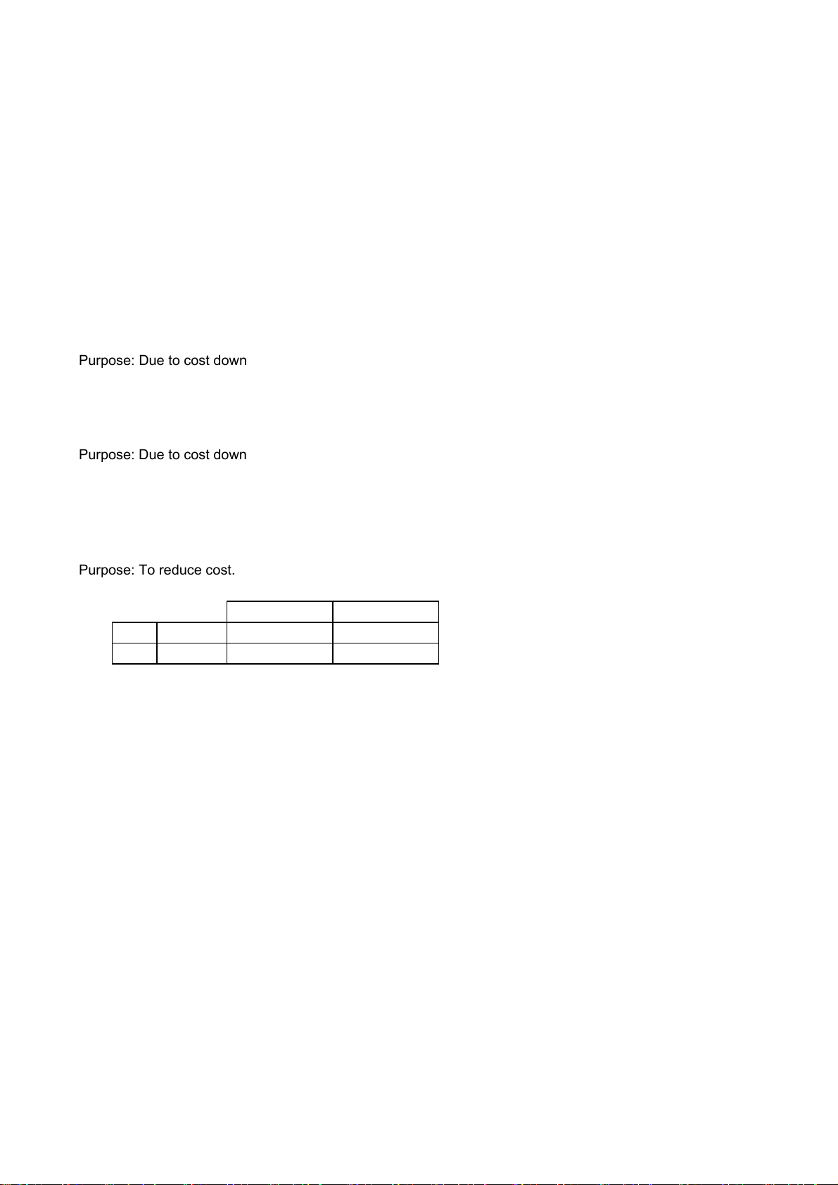
3. X Drive MASK Module IC
G5: Using 2 ICs --> G6 : Using 1 IC
Purpose: Due to cost down
Because Sustain pulse was slightly changed, SUS-Clamp boards were added.
4. Change of SCAN IC
Purpose: To reduce cost.
5G 6G
50" Panasonic
43" TI SN755866PZP SN755870PZT
AN16021AA AN16025A
Page 12
Difference of waveform between G5 and G6
)
P
N
e
12
VPRST
Can be
up to
350V
G5 G6
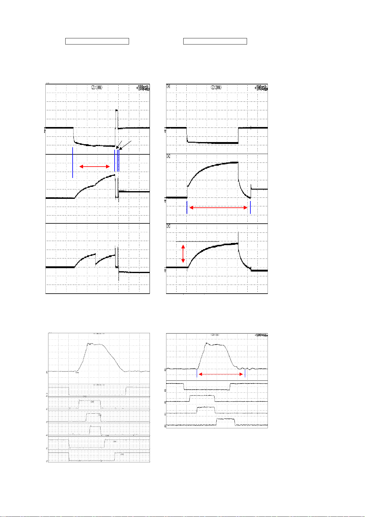
Reset waveform
3 times reset → 1 time reset (Improve dark brightness
Reset voltage of Y drive (Plus voltage) U
Reset voltage of X drive (Minus voltage) DOW
XPSUS XPSUS
②③
100V/DIV 100V/DIV
SCAN out
①
SCAN out
①
YPSUS
Sustain waveform
2 step resonance → 1 step resonanc
Vsus voltage LESS
Sustain pulse cycle SHORTER
SUS-G
SUS-U1
SUS-U2
SUS-B
100V/DIV
100V/DIV
YPSUS
PSUSPSUS
Pulse width of G5
SUS-G
SUS-U
SUS-B
SUS-D
SUS-D2
SUS-D1
Page 13
Comparison Drive Assy between G5 and G6
13
(Block diagram)
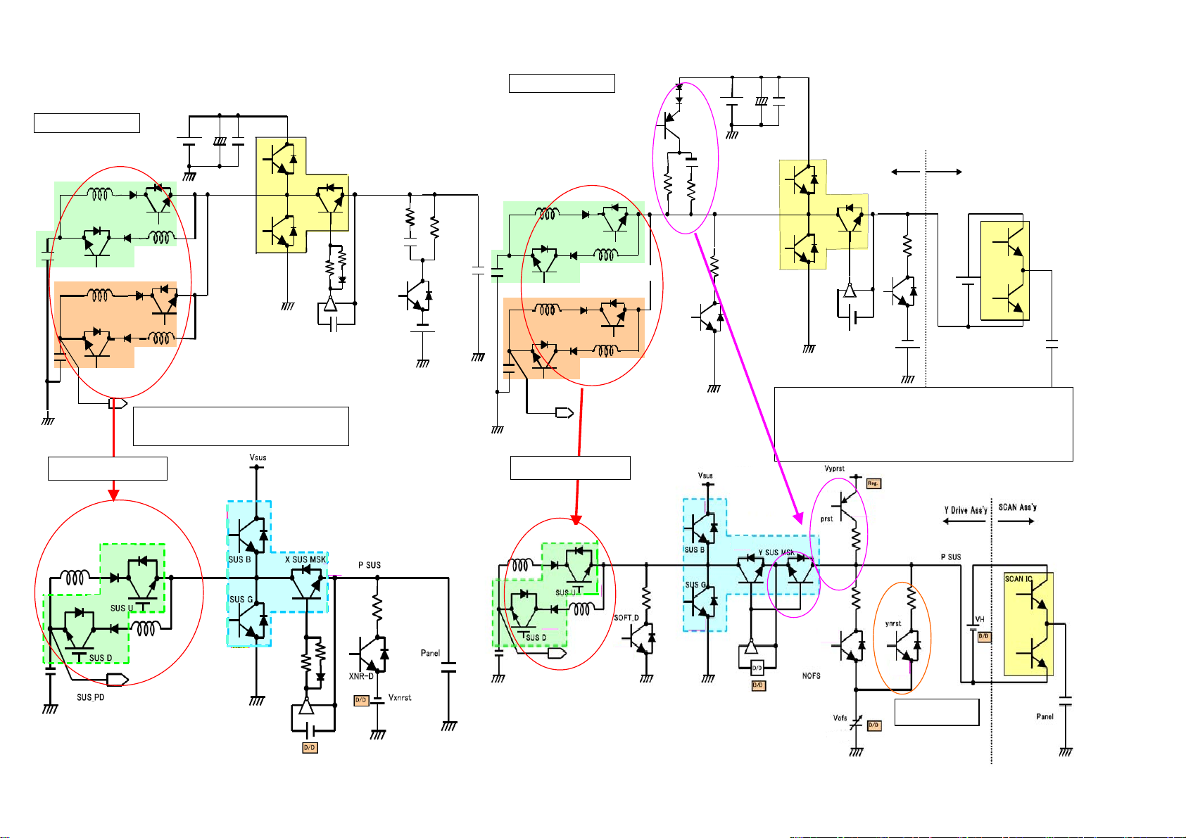
X Drive Assy for G5
Vsus
SUS D2
223V
SUS B
SUS G
SUS U2
2nd Resonance
MASK Module
X SUS MSK
RN D
P SUS
Y Drive Assy for G5
Panel
SUS D2
SUS U2
2nd Resonance
共振2段目
PR-U
SOFT_D
Vsus
434:215V
504:223V
SUS B
SUS G
MASK Module
Y SUS MSK
Y Drive A ss'ySCAN Ass'y
Y Drive Ass'y
P SUS
P SUS
130V
SCAN IC
VH
SUS U1
1st Resonance
SUS D1
中点電位検出回路へ(既定電圧幅
より上がっても下がってもPD)
2 Step Resonance→1 Step Resonance
Discreet Structure→DK Module
X Drive Assy for G6
Resonance Module
( DK Module)
X Mask Module
Vrn
-230V
SUS U1
SUS D1
共振1段目
1st Resonance
To detecting midpoint voltage
PD should occur if this voltage is over or
below from specified value.
Y Drive Assy for G6
DK Module
To detecting midpoint
voltage circuit
Plus reset voltage G5: VSUS → G6:Reserved power
supply
Since the value of Plus Reset Voltage became beyond the
value of VSUS, Plus Reset connect to PSUS and SUSMSK
became two-way.
Y Mask Module
VF
Vofs
Vofs
-30V
-30V
~-52V
~-52V
Panel
Added circuit
for Minus Reset
Page 14
Board Differences between G5 and G6
14
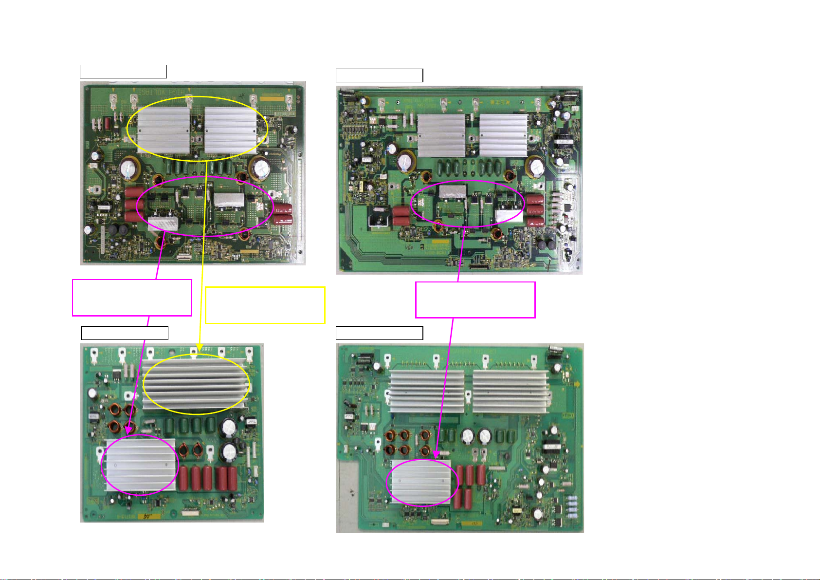
G5 X Drive Assy
G5 :Discrete circuit
G6: DK Module IC
G6 X Drive Assy
G5 : Two Mask Module ICs
G6: One Mask Module IC
G5 Y Drive Assy
G5 :Discrete circuit
G6: DK Module IC
G6 Y Drive Assy
Page 15
Power Supply map of X and Y Drive ASSY
to Add
'y
f
ly
f
ly
Y Dri
X Dri
Note:to Add
'y
e
A
N
15
200v
Voltage level Depends on Panel.
ress Ass
Logic
DK
Mod.
Mask
Mod.
Ofset
Reset
Scan
Logic
ve Assy
Vprst
5.0V
VOFS
VF
IC5V
VPRST
Reg.
VH
5.0V 6.5V
5V
Reg.I
16.5V
VSUS
VOFS
DC/DC Conv.
IC5V
DC/DC Conv.
VH
DC/DC Conv.
rom P Supp
Reset
Mask
Mod.
Logic
DK
Mod.
ve Assy
VRN
VRN
DC/DC Conv.
15V
DC/DC Conv.
5.0V
5V
Reg.
rom P Supp
VSUS 16.5V 6.5V
Scan Assy
Scan IC
ress Ass
DC/DC converter, for VOFS, and regulator of VPRST ar
controlled by Electric Volume.
lthough, basically, each DC/DC converter for VOFS and VR
is inputted 16.5V, as Vcc, they are not active if VSUS is below 100V
Page 16
50 SCAN A and B ASSYS
16
IC2801
Scan IC
IC2802
Scan IC
IC2803
Scan IC
IC2804
Scan IC
IC2805
Scan IC
IC2806
Scan IC
Scan Signal
VH
IC5V
PSUS
50 SCAN B ASSY
(UPPER)
SB1
IC2701
Scan IC
IC2702
Scan IC
IC2703
Scan IC
IC2704
Scan IC
IC2705
Scan IC
CN2802
Serial Data
CN2702
IC2706
Scan IC
PSUS
IC5V
VH
Scan Signal
SA1
50 SCAN A ASSY
(LOWER)
Page 17

Blank Page
Page 18
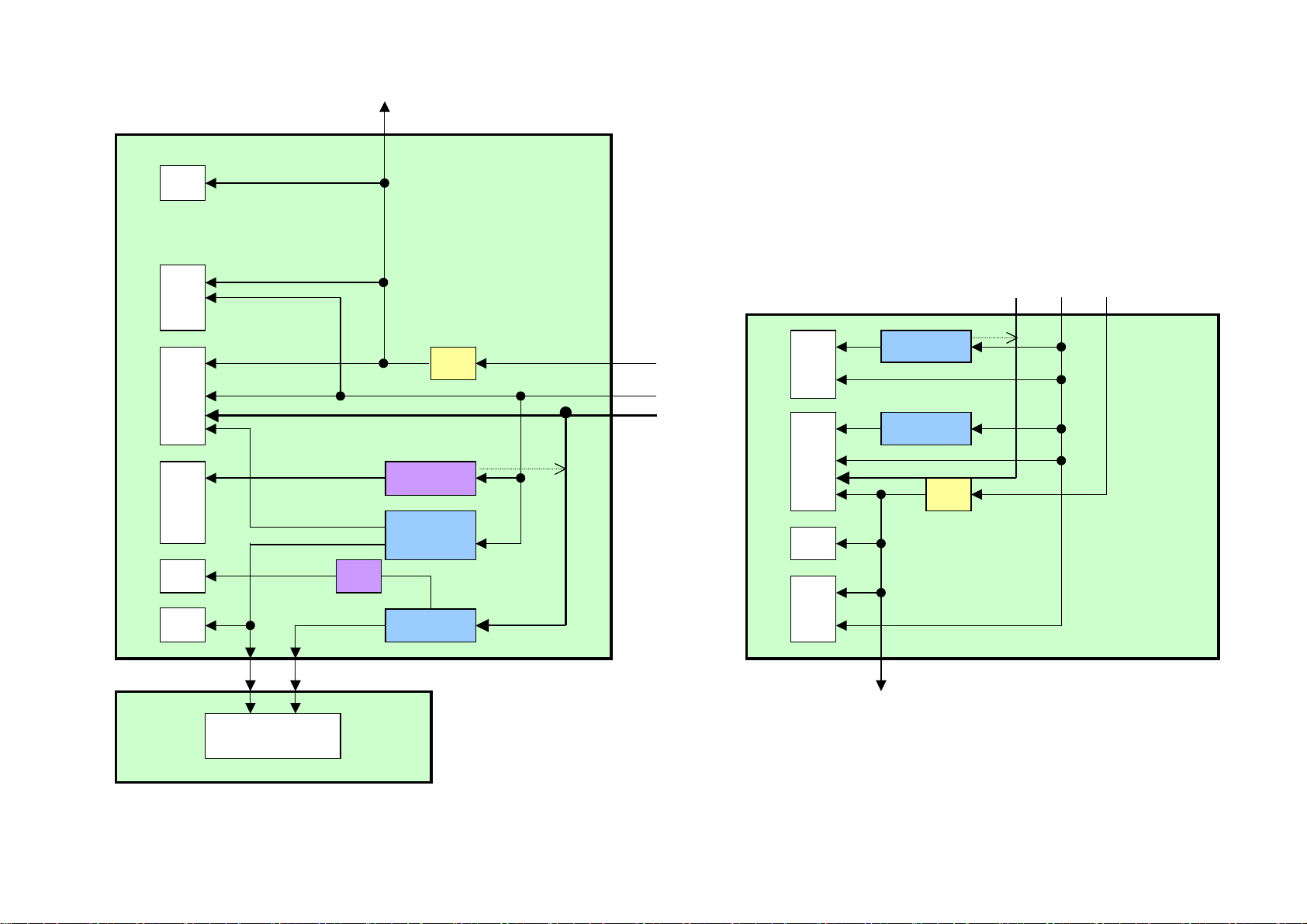
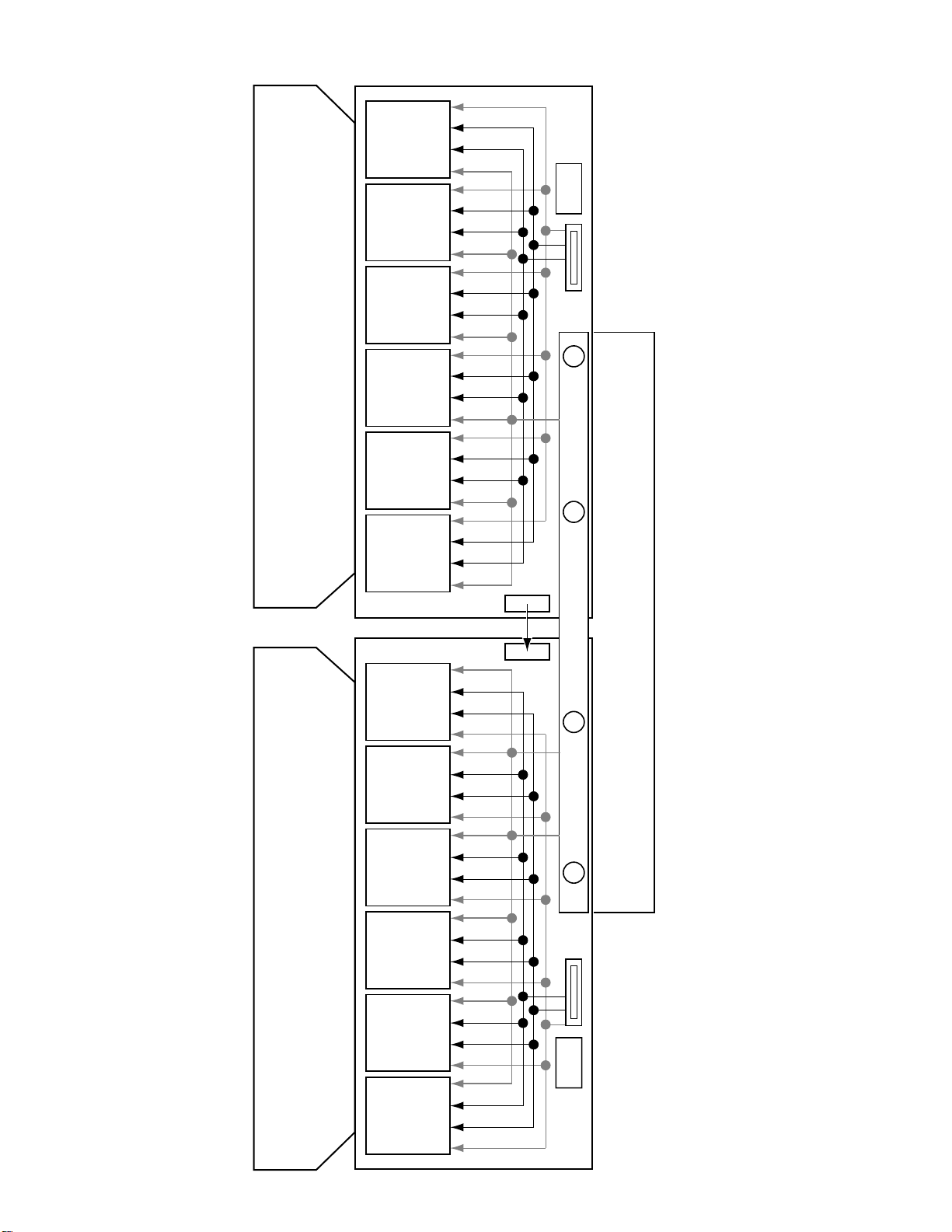
SCAN IC - 43 Inch Models
18
List of IC
SN755870PZT, TC7SH08FUS1, TC74VHC00FTS1, AXF1143, AXF1145, TC74VHC08FTS1, AXF1144, M62334FP,
TC74VHC123AFTS1, PST3610UR, PEG122C, NJW1183L
SN755870PZT (43 SCAN A ASSY : IC2701 - IC2706)
(43 SCAN B ASSY : IC2801 - IC2806)
• Plasma Display Panel IC
Pin Arrangement (Top view)
OUT2100
OUT199
N.C.98
VDDH97
VDDH96
N.C.95
GND194
GND193
CLR92
SI91
OC290
OC189
VDD88
LAT87
CLK86
SO85
DIR84
GND183
GND182
N.C.81
VDDH80
VDDH79
N.C.78
OUT6477
OUT6376
Block Diagram
1OUT3
2OUT4
3OUT5
4OUT6
5OUT7
6OUT8
7OUT9
8OUT10
9OUT11
10OUT12
11OUT13
12OUT14
13OUT15
14OUT16
15OUT17
16OUT18
17OUT19
18OUT20
19OUT21
20OUT22
21OUT23
22OUT24
23OUT25
24OUT26
25OUT27
26OUT28
27OUT29
28OUT30
29OUT31
30OUT32
31N.C.
32VDDH
33VDDH
34N.C.
35GND1
36GND1
37GND1
38N.C.
DD
V
88
39GND2
40GND1
41GND1
42N.C.
43VDDH
44VDDH
45N.C.
46OUT33
47OUT34
48OUT35
49OUT36
50OUT37
VDDH
DDH
V
OUT6275
OUT6174
OUT6073
OUT5972
OUT5871
OUT5770
OUT5669
OUT5568
OUT5467
OUT5366
OUT5265
OUT5164
OUT5063
OUT4962
OUT4861
OUT4760
OUT4659
OUT4558
OUT4457
OUT4356
OUT4255
OUT4154
OUT4053
OUT3952
OUT3851
SO
GND2
DK
DA
DK
DA
DK
DA
GND1
46-76,
GND1
99
1-30,
100
77
OUT1
OUT2 - OUT63
OUT64
Level
Shift
91
SI
64-bit Shift Register
85
DIR
9284
CLR
86
CLK
Data
64-bit Latch
Data
87
LAT
OC1
Circuit
Level
Shift
Circuit
Output Control Circuit
Level
Shift
Circuit
9089
OC2
Page 19
Pin Function
19
No. Pin Name I/O Pin Function
1 - 30 OUT3 - OUT32 O High-voltage push-pull output
31 N.C. − Not connected
32 - 33 V
34 N.C. − Not connected
35 - 37 GND1 − Ground
38 N.C. − Not connected
39 GND2 − Ground
40 - 41 GND1 − Ground
42 N.C. − Not connected
43 - 44 V
45 N.C. − Not connected
46 - 77 OUT33 - OUT64 O High-voltage push-pull output
78 N.C. − Not connected
79 - 80 V
81 N.C. − Not connected
82 - 83 GND1 − Ground
84 DIR I
85 SO I/O Serial data input / output
86 CLK I Serial clock input Fetch SI or SO data to shift register by CLK rise edge
87 LAT I
88 V
DDH − High-voltage circuit supply
DDH − High-voltage circuit supply
DDH − High-voltage circuit supply
Setup of shift register shift direction
L = Shift into reverse (SO → SI) H = Shift forward (SI → SO)
LAT data input
L = Transfer shift register data to output latch H = Hold data to output latch
DD − Logic supply
89 OC1 I
Output control
Control output according to the right
truth value table
90 OC2 I
OC1 OC2 OUT
LLALL Hi-Z
LH DATA
HL ALL L
HH ALL H
91 SI I/O Serial data input / output
92 CLR I All output reset CLR pin : L → Normal operation CLR pin : H → All output High
93 - 94 GND1 − Ground
95 N.C. − Not connected
96 - 97 V
DDH − High-voltage circuit supply
98 N.C. − Not connected
99 - 100 OUT1 - OUT2 O High-voltage push-pull output
Page 20

SCAN IC - 50 Inch Models
20
•
List of IC
AN16025A, TC7SH08FUS1, TC74VHC00FTS1, AXF1140, AXF1142, TC74VHC08FTS1, AXF1141, M62334FP,
TC74VHC123AFTS1, PST3610UR, PEG122C, NJW1183L
AN16025A (50 SCAN A ASSY : IC2701 - IC2706)
(50 SCAN B ASSY : IC2801 - IC2806)
• Plasma Display Panel IC
Pin Arrangement (Top view)
OUT2100
OUT199
N.C.98
VDDH97
VDDH96
N.C.95
GND194
GND193
CLR92
SI91
OC290
OC189
VDD88
LAT87
CLK86
SO85
DIR84
GND183
GND182
N.C.81
VDDH80
VDDH79
N.C.78
OUT6477
OUT6376
Block Diagram
1OUT3
2OUT4
3OUT5
4OUT6
5OUT7
6OUT8
7OUT9
8OUT10
9OUT11
10OUT12
11OUT13
12OUT14
13OUT15
14OUT16
15OUT17
16OUT18
17OUT19
18OUT20
19OUT21
20OUT22
21OUT23
22OUT24
23OUT25
24OUT26
25OUT27
26OUT28
27OUT29
28OUT30
29OUT31
30OUT32
31N.C.
32VDDH
33VDDH
34N.C.
35GND1
36GND1
37GND1
38N.C.
DD
V
88
39GND2
40GND1
41GND1
42N.C.
43VDDH
44VDDH
45N.C.
46OUT33
47OUT34
48OUT35
49OUT36
50OUT37
VDDH
DDH
V
OUT6275
OUT6174
OUT6073
OUT5972
OUT5871
OUT5770
OUT5669
OUT5568
OUT5467
OUT5366
OUT5265
OUT5164
OUT5063
OUT4962
OUT4861
OUT4760
OUT4659
OUT4558
OUT4457
OUT4356
OUT4255
OUT4154
OUT4053
OUT3952
OUT3851
SO
GND2
DK
DA
DK
DA
DK
DA
GND1
46-76,
GND1
99
1-30,
100
77
OUT1
OUT2 - OUT63
OUT64
Level
Shift
91
SI
64-bit Shift Register
85
DIR
9284
CLR
86
CLK
Data
64-bit Latch
Data
87
LAT
OC1
Circuit
Level
Shift
Circuit
Output Control Circuit
Level
Shift
Circuit
9089
OC2
Page 21

Pin Function
21
No. Pin Name I/O Pin Function
1 - 30 OUT3 - OUT32 O High-voltage push-pull output
31 N.C. − Not connected
32 - 33 V
34 N.C. − Not connected
35 - 37 GND1 − Ground
38 N.C. − Not connected
39 GND2 − Ground
40 - 41 GND1 − Ground
42 N.C. − Not connected
43 - 44 V
45 N.C. − Not connected
46 - 77 OUT33 - OUT64 O High-voltage push-pull output
78 N.C. − Not connected
79 - 80 V
81 N.C. − Not connected
82 - 83 GND1 − Ground
84 DIR I
85 SO I/O Serial data input / output
86 CLK I Serial clock input Fetch SI or SO data to shift register by CLK rise edge
87 LAT I
88 V
DDH − High-voltage circuit supply
DDH − High-voltage circuit supply
DDH − High-voltage circuit supply
Setup of shift register shift direction
L = Shift into reverse (SO → SI) H = Shift forward (SI → SO)
LAT data input
L = Transfer shift register data to output latch H = Hold data to output latch
DD − Logic supply
89 OC1 I
Output control
Control output according to the right
truth value table
90 OC2 I
OC1 OC2 OUT
LLALL Hi-Z
LH DATA
HL ALL L
HH ALL H
91 SI I/O Serial data input / output
92 CLR I All output reset CLR pin : L → Normal operation CLR pin : H → All output High
93 - 94 GND1 − Ground
95 N.C. − Not connected
96 - 97 V
DDH − High-voltage circuit supply
98 N.C. − Not connected
99 - 100 OUT1 - OUT2 O High-voltage push-pull output
Page 22

Simplified Circuit of G6 ADDRESS
22
ADR B
ADR U
ADR OUT
Detective
circuit
ACTIVE HIGH
Vadr
60V
ADR D
ADR Module
(TCP)
Panel
<<Feature of G6 address>> <<Change from G5>>
Single addressing drive Vadr 61V to 60V
Old: 8 PCB (Top side and bottom side) 9V to 8V
New: 4 PCB (Bottom side) 2 connector of Power and Signal
Add TCP heat sink FFC LVDS transmission 3.3V 8V
New TCP (Address IC's) Cord 60V/5V
Clock frequency:102.5MHz PD circuit
Double edge clock Old: Detecting over current
New: Watching voltage
ADR PD
Page 23

pp
Simplified Address System Drawing for G6
23
5V
(Power for TCP)
Y-Drive
60V
X-Drive
FFC LVDS transmission
3.3V(Power for LVDS receiver)
8V(Power for FET, in address resonance)
Digital
Assy
60V
5V
(Power for TCP)
Address
Note: 60V(power for Address) and 5V(power for TCP) are supplied through X and Y Drive Assy.
The signal of LVDS, 3.3V(power for LVDS receiver) and 8V(power for FET, address resonance)
are su
lied through Digital Assy.
Address
Address
Address
Page 24

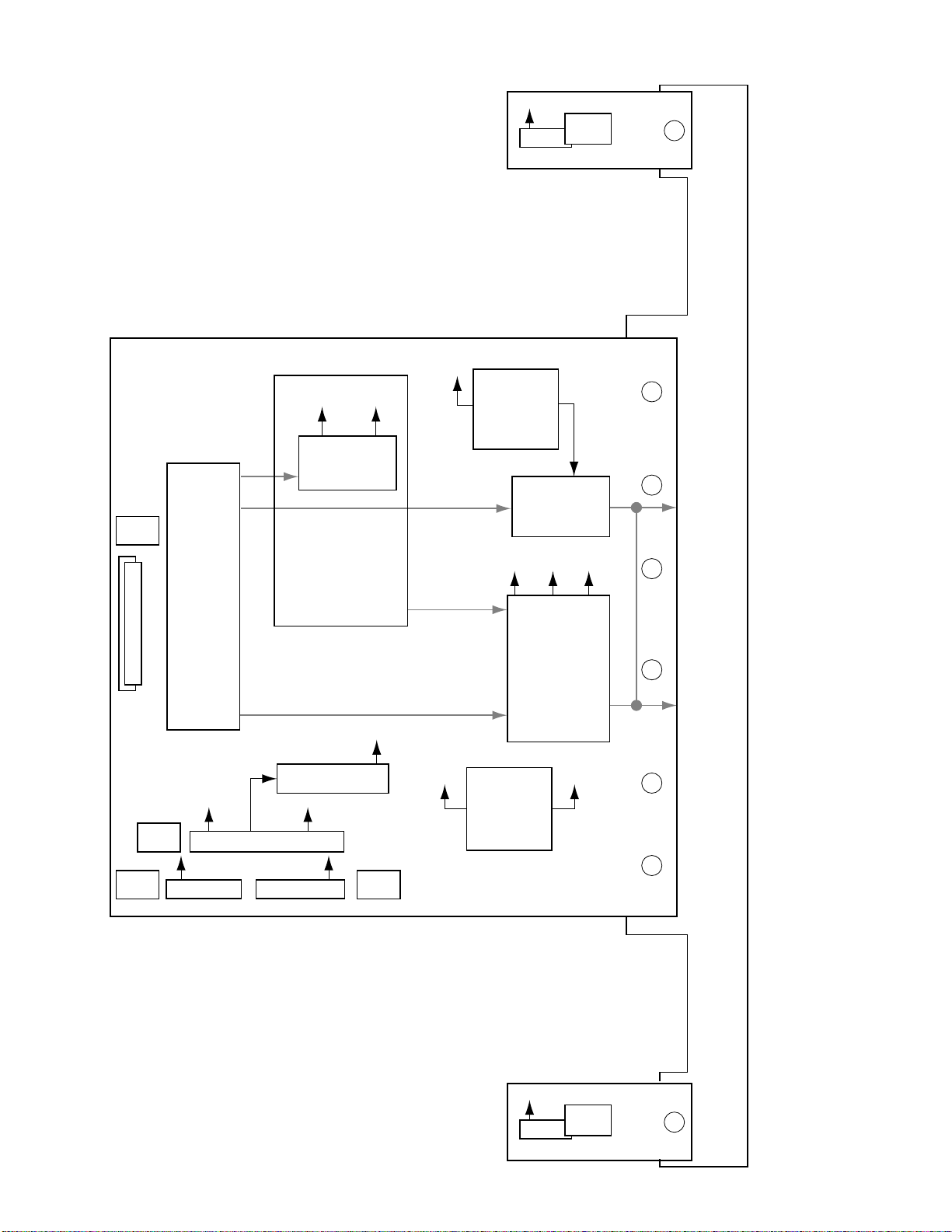
50 ADDRESS ASSY
24
AD1 AD2
V+8V
Resonance
Block
V+ADR5
IC1555
Driver IC
CN1501
AN/P BN/P
CN/P DN/P CLKN/P
Resonance
IC1554
Driver IC
Block
V+ADR4
V+3V
IC1501
(PEE002A-K)
LVDS Receiver
Resonance
Block
V+ADR3
IC1553
Driver IC
CN1502
V+60VV+5V
Resonance
CLK/LE/HBLK/LBLK
R/G/B
Block
V+ADR2
IC1552
Driver IC
Resonance
Block
V+ADR1
IC1551
Driver IC
Page 25

Block diagram of Address circuit of 43 inch PDP
25
DRIVER IC
IC1552
V+ADR1
RESONANCE
BLOCK
V+60V
V+5V
DRIVER IC
IC1553
DRIVER IC
IC1501
LVDS RECEI
VER
IC1554
CLK / LE / HBLK / LBLK
R/G/B
DRIVER IC
IC1555
V+ADR5
RESONANCE
BLOCK
V+8V
AD2
CN1502
V+3V
AN/P BN/P
CN/P DN/P CLKN/P
AD1
CN1501
Page 26

HD AUDIO Assy and other Assy
A
A
Y
Y
Y
y
t
y
y
y
y
26
- Differences between G4 / G5 and G6 2005.07.28
Content G4 /G5 AUDIO Assy G6 AUDIO Assy MEMO
1. Change of Surround IC and NJM2195L + BD3869AS NJW1183L SRS IC and VOL IC are changed one chip IC
VOL IC (IC3753) due to cost down
2. Change of IC control NJW2195L ⇒ Port control NJW1183L ⇒ IIC Using only IIC control
BD3869AS ⇒ IIC control
3. Change of SP terminal AKE1060-
4. Change of AUDIO assembly
construction + SP TERMINAL ASS'
5. EEP ROM for Backup On HD PANEL IF ASS'
- Differences between 43 inch and 50 inch : None
- Audio output during Service Factory mode: None
UDIO AMP ASS'Y HD AUDIO ASS'
KE1061- G5: Under-Angle type
G6: Straight-Angle type
One board construction due to cost down
On HD AUDIO ASS'YDue to deletion of PANEL IF Ass
- Other small assemblies:
* LED Assy Change of LED color during Power On ( Green --> Blue )
* IR Assy IR unit was changed to G4 IR uni
* TEMP SENSOR Ass
* KEY Ass
KEY TERMINAL Ass
( No circuit change )
Move to DIGITAL VIDEO Ass
Deleted
( Move to front panel of Media Receiver )
Page 27

A2
27
+16.5V
HD AUDIO ASSY
+16.5V
+16.5V
IC3752
Regulator
+9.0V
+9.0V
Buffer
+9.0V
R_OUT +
Right
IC3751
Power Amp IC
R_OUT –
L_OUT +
SP TERMINAL
L_OUT –
Left
DC Detect
Block
A3
WOW + Volume IC
+3.3V
IC3753
EEP ROM
IC3754
SCL
SDA
+3.3V
A_Mute
A_STBY_B
R_Audio
L_Audio
A_NG_B
SDA
SCL
A2
SPEAKERS
Page 28

P1
28
200v
To Address
P2
P7
+60V
VSUS
+16.5V
+6.5V
VSUS_CONT
IC202
POWER SUPPLY UNIT
SECONDARY PRIMARY
Switching
T702
T902
Q703
Q704
Switching
Switching
Q901
Q902
Switching
+390V
PFC Q101
Q102
Q103
D109
D103
P6
P5
RELAY
P4
+16.5V
VSUS_ADJ
+8V
STA3.3V
PS_PD
EXT_PD
T502
T101
RY102
Switching
Q501
Q502
Switching
IC101
Switching
D107, D108
P3
NEUTRAL
LIVE
Page 29

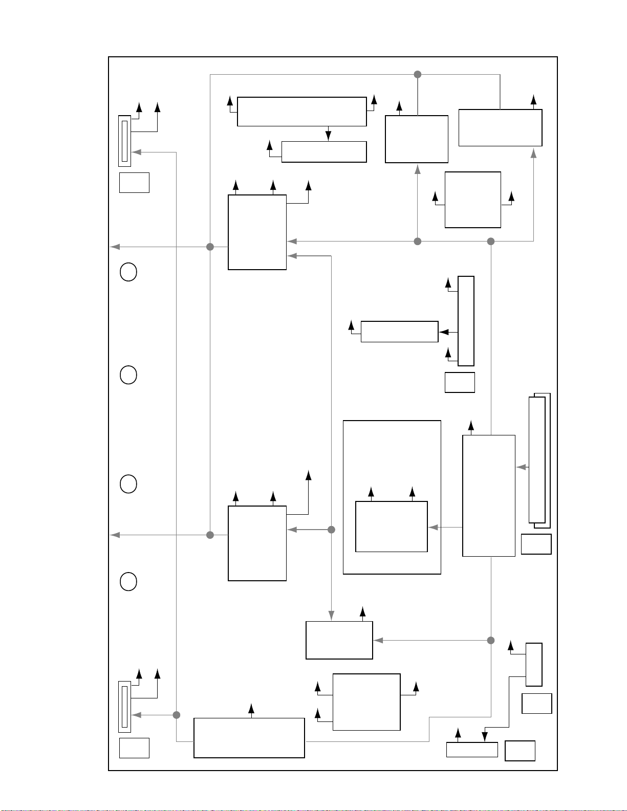
GENERAL INFORMATION
29
PCB LOCATION
SUS CLAMP 1 Assy
50 Y DRIVE Assy50 SCAN B Assy
POWER SUPPLY Unit
50 X DRIVE Assy
50 SCAN A Assy
50 ADDRESS Assy50 ADDRESS Assy 50 ADDRESS Assy 50 ADDRESS Assy
HD LED
Assy
HD AUDIO Assy HD DIGITAL Assy SUS CLAMP 2 AssyHD IR Assy
Page 30

DIAGNOSIS OF SHUTDOWN/POWER-DOWN INDICATED BY LEDS
30
(RED LED)
(BLUE LED)
Deleted
• Operation statuses as indicated by LEDs On The Panel
Status LED Pattern
Standby
Power ON
AC Power OFF of
one side
System cable
disconnection
Power-down
Shutdown
No backup copy
Lit in Red1
Lit in Blue2
Red flashes
3
(1000ms)
Red and
blue flash
4
(1000ms)
Red flashes
5
(500+2500ms)
Blue flashes
6
(500+2500ms)
Lit in Red and
7
blue flashes
(200ms)
Blue
Red
Blue
Red
Blue
Red
1000ms
Blue
1000ms
Red
Blue
Once
Red
500ms
Blue
500ms
Red
Once Twice
200ms
Blue
Red
: Lit in Red LED
: Lit in Blue LED
Twice
• PD (power-down) count
1 Not used
2 POWER SUPPLY Unit
3 SCAN Assy
4 5V power supply for SCAN
5 Y-DRIVE
6 DCDC for Y drive
7 Y-SUS
8 ADDRESS Assy
9 X-DRIVE
10 DCDC for X drive
11 X-SUS
12 Not used
13 Sequence drive stop
14 Not used
15 UNKNOWN
Note:
• When a shutdown occurs, a warning will be issued by the
Media Receiver and displayed, then the power will be shut off.
• When a shutdown or power-down occurs on the Panel side,
the Media Receiver will enter Standby mode (the red LED
will light).
1000ms
n times
n times
2.5s
2.5s
Once
Once
• SD (shut down) count
1 SEQUENCE PROCESSOR (SQ_IC)
2 MDU-IIC
3 RST2 abnormality
4 Panel high temperature
5 Speaker short-circuit *
* When a jumper (J110) between the HD AUDIO Assy and
the HD DIGITAL Assy is disconnected, the SD LED
flashes in this manner.
Page 31

Y Drive PD system(6G)
31
(Power Down System - RED Flashing LED on Panel)
130v
VH
IC5V
Detection of
SCAN Upper
connection
Detection of
SCAN Lower
connection
VOFS
VPrst
UVP
Detection
UVP
Detection
Voltage
Detection
Deletion of 16.5 V detection circuit (YDRIVE_PD)
Voltage
Detection
Voltage
Detection
SCAN_PD
( 3 times PD )
SCN5V_PD
( 4 times PD )
( 5 times PD )
Y_DD_PD
( 6 times PD )
Middle-point
Voltage of
resonance
Comparison
to standard
( Sustain )
X Drive PD system(6G)
16.5V
VRN
VF15V
voltage
OCP
detection
Deletion of this
detection circuit
UVP
Detection
UVP
Detection
YSUS_PD
( 7 times PD )
XDRIVE_PD
( 9 times PD )
Only detecting
disconnection
of FFC
XDD_PD
( 10 times PD )
Middle-point
Voltage of
resonance
( Sustain )
Comparison
to standard
voltage
XSUS_PD
( 11 times PD )
NOTE UVP: Under Voltage Protection, OCP: Over Current Protection
Page 32

Power Down diagnosis ( defective points)
T
32
(RED FLASHING LED)
Number of PD circuit in Reason for PD
Blinking operation
2 times POWER P SUPPLY Ass'y
3 times
4 times
6 times
7 times Y-SUS Y DRIVE Ass'y
8 times
9 times X-DRIVE X DRIVE Ass'y CN1201
10 times X-DCDC
SCAN
SCN-5V
Y-DCDC Y DRIVE Ass'y
ADRS ADDRESS Ass'y
Defective PBC Assy
SCAN Ass'y
Y DRIVE Ass'y
SCAN Ass'y
Y DRIVE Ass'y IC5V DC/DC Q2605,R2647
X DRIVE Ass'y
(Power-down) Point to be Checked Possible Defective Part Remark
SCAN IC SCAN IC VH-GNDH
VH UVP
Detection of cable detection CN2001, CN2350
Detection of cable detection
IC5V UVP
VOFS UVP
Vprst UVP Vprst Regulator Q2531,Q2532,IC2535
PD cuased by dtection of
Sustain middle-point voltage
Address Power Down
Detection of cable detection
VRN UVP
PD cuased by dtection of
Sustain middle-point voltage
DDRESS RESONANCE BLOCKD1634
Y SUS BLOCK IC2252,IC2253
VH DC/DC IC2502,L2501
CN2401, CN2402
SCAN IC SCAN IC
VOFS DC/DC Q2606,R2619,R2620
Y SUS BLOCK IC2252,IC2253,Q2280,Q2281
Y RESONANCE BLOCK IC2101
Y SUS BLOCK Q2221
VRN DC/DC Q1323,R1332,R1333
X SUS BLOCK Q1272
X RESONANCE BLOCK IC110111 times X-SUS X DRIVE Ass'y
VSUS-SUSOUT, SUSOUTSUSGND
MSKS-SUSOUT
V+ADR-GND_ADR
CN1501
OVP : OVER VOLTAGE PROTEC
UVP : UNDER VOLTAGE PROTECT
Page 33

Assumed symptom from PD mode
33
Blinking PD circuit Check portion Main symptom Remarks
2 Power PD Power Supply
Scan Ass'y Short between VH and GNDH, Scan IC PD with panel briefly flashing
Malfunction of DC/DC converter, for VH PD with panel briefly flashing
Short between VSUS, SUSOUT, or SUSGND, Mask
3 SCAN PD
4 IC5V PD
5 Y-DRIVE PD Delete detection circuit
6 Y DCDC PD Y Drive Assy
7
8 Address PD Address Assy
9 X-DRIVE PD X Drive Assy
10
11 X SUS PD X Drive Assy
X DCDC PD X Drive Assy
Y Drive Assy
X Drive Assy
SCAN Ass'y Short between IC5V and GNDH, Scan IC
Y Drive Assy
Y Drive AssyY SUS PD
Module
Disconnect connector between Y Drive and Power
Supply, or Digital Assy.
Short between VSUS, SUSOUT, or SUSGND, Mask
Module
Disconnect bridge connector, between Scan Assy and
Y Drive,
R2352 open (16.5V line resistor) PD without panel flashing
Malfunction of DC/DC converter, for IC5V
Short between PSUS and MSKS, Mask Module
Short between MSKS and SUSOUT, Mask Module PD with panel briefly flashing
Malfunction of DC/DC converter, for VOFS
Malfunction of Regulator of Vprst
Malfunction of DK module
Control signal line problem
Disconnect Flexible cable, between Digital Assy and X
Drive
Disconnect connector between X Drive and Power
Supply
Malfunction of DC/DC converter, for VRN
R1204 open (16.5V line resistor) PD without panel flashing
Malfunction of DK module
Control signal line problem
PD without panel flashing
PD without panel flashing
PD without panel flashing
Page 34

Diagnosis method for 3 times flashing PD
34
Diagnose 3 times flashing PD according to the steps below
1. Visual check with Power off condition
2. Impedance check with power off condition
3. Voltage check with power on condition
Actual diagnosis methods are as follows
1. Visual check with Power off condition
Check the all of connectors and FFC on Y Drive Assy whether completely connected
2. Impedance check with power off condition
i ) Impedance check between Vsus - SUSGND on Power Supply Assy
If the impedance is several hundreds k ohm or over -> go to step " ii "
If the impedance is short circuit -> Remove P1 and P2 connectors and check impedance
between Vsus - SUSGND on X Drive and Y Drive Assy.
Vsus - SUSGND impedance check on X and Y Drive Assy with no Vsus cables
If the impedance on X Drive Assy is short circuit → Replace X Drive Assy
Vsus-SUSOUT or SUSOUT-SUSGND are short circuit : Defective of X MASK module IC
Other than above : defective of other devices
Follow check steps below.
If the impedance on Y Drive Assy is short circuit → Replace Y Drive Assy
Vsus-SUSOUT or SUSOUT-SUSGND are short circuit : Defective of Y MASK module IC
Other than above : defective of other devices
If the impedance on Power Supply Assy is short circuit → Replace Power Supply Assy
NOTE: Because some capacitors have voltage, it seems impedance is short just after
measuring of impedance by multimeter.
Actually if no short circuit , the impedance is soon going up.
ii ) Impedance check between VH - PSUS on Y DRIVE Assy
If the impedance is several M ohm or over -> go to step 3
If the impedance is short circuit -> Remove bridge connectors between Y Drive Assy and Scan A or
B Assy and check it again at Y drive, Scan A and Scan B Assy.
Short circuit on Scan A Assy -> Scan IC on Scan A Assy is defective
Short circuit on Scan B Assy -> Scan IC on Scan B Assy is defective
Short circuit on Y Drive Assy -> Defective of Y Drive Assy
3. Voltage check with power on condition before PD is working
Vsus voltage is not going up to around 200 V -> Defective of Power Supply Assy
VH voltage is not going up to around 130 V -> Defective of DC-DC converter on Y Drive Assy
4. Check of Power Down detection circuit
If there is no problem step 1, 2, and 3, both of VH voltage and VSUS voltage are normal, but PD
circuit is working. Therefore PD detection circuit has problem.
-> Replace Y Drive Assy : because detection circuits for 3 times PD are on Y Drive Assy
Page 35

The list of possible defective parts
A
A
35
(Address PD : Red LED blinks 8 times)
Parts# and mark
50 inch 43 inch
HAT1110R
Q1614 etc. Q1609 etc.
UDZS15(B)
D1605 etc. D1620 etc.
EP05FA20
D1634 etc. D1608 etc.
CH1405
C1602 etc. C1602 etc.
2SA1163
Q1613 Q1612
RN1901
Q1612 Q1615
disconnecting connector
CH1422
Description
FET
Zener Diode
Diode
φ10 Chemical
Condenser
Transistor
Digital Transistor
FFC disconnecting connector
Defective mode
Short or Open between
D(Drain) and S(Source)
Short or Open
Short or Open
Short
Short or Open
Short or Open
Page 36

・
B
Q
p
.
36
lock diagram of the shutdown signal
Note:
The figures ① - ⑤ indicate the
number of times the LED flashes
when sutdown occurs in the
corres
onding route
HD DIGITAL ASSY
HD AUDIO ASSY
D3
A2
IC3504
AMP
IC3754
EEPROM
IC3753
VOLUME IC
A_NG
⑤
IC3157
DAC IC
IC3001
DVI REIVER
・Diagnosis of shutdown
TXD_SQ
RXD_SQ
CLK_SQ
BUSY S
②
SCL
SDA
CE_SQ
IC3401
sequence
processor
①
IC5201
Module Ucom
RST2
③
IC3303
OR
②
E_SCL
E_SDA
TEMP1
IC3302
3.3V-RST
IC3304
1.2V-RST
IC3156
EEPROM
④
TEMP SENSOR
IC3158
Number of
flashes
1 time
2 tim es
3 tim es
4 times
5 tim es
SD Cirsuit in Operation Defective Assy Reason for Shutdown
Communication fai lure of IC3401
Communication fai lure
of the driving processor
Communication fai lure
of the IICline (C heck the
SD subcategory on the
Factory Menu.)
Power failure of the
drivi ng proc es sor
(RST2)
Abnormally hig h
temperature of the pa n el
Audi o f a ilure
HD DIGITAL
HD DIGITAL
HD AUDIO
HD DIGITAL
POWER SUPPLY the 8-V power supply is not activated.
HD AUDIO Defective AMP IC HD AUDIO ASSY IC3751
HD AUDIO Disconnection of connectors A1- P5
Writing failur e of IC3401
Communicatio n fai lure of the EEPROM
(for retaining 4-Kbyte of data)
Communication error of DAC IC MODULE UCOM BLOC
Communication error of DVI Re ceiver IC TMDS RX BLOC
Communicatio n fai lure of the EEPROM
(for retaining 4-Kbyte of data)
Disconnection of connectors A2-D3
Defective volume IC HD AUDIO ASSY IC3753
Defective DC-DC converter DIGITAL DD CON BLOCKU3601
Defective RST IC PANEL FLASH BL OCK IC3302-IC3304
Defective IC3401 SQ ASIC BLOCK IC3401
Abnormally high temperature of the panel Ambient temperature
Grounding fault of speaker out puts
Point to be checked
SQ ASIC BLOCK,
PANEL FLASH BLOC
MODULE UCOM BLOCK IC3156
K IC3001
PANEL IF BL OCK IC3754
Defective Part
IC3401, IC3301
K
K IC3157
Possidle
Remarks
Check if versi on data can be
read,using the
"GS1"command,after the
power is turned on again.
Check if the connectors are
disconn ec te d or are not
connecte d secu r el
Check if 3.3-V and 1.5-V
power supplies are activated.
Check if the 8-V power is
supplied at Pin 1 of the D11
connector.
The pane l wil l be shutdown i
the senso r de tec ts temperature
of 75℃ or higher (for the
PDP-436P/-506P
Check if the speaker cables
are in contact with the
chassis,etc.
Check if connectors are
disconn ent ed or are not
connecte d secu r ely.
y.
).
f
Page 37

- Attention point for repair
37
Since G6 Audio IC is BLT type of Power IC as same as G4 and G5 Audio IC,
both of speaker outputs ( plus and minus ) always have about 7 V DC.
Therefore do not short between speaker minus and GND like the following figure.
Otherwise Power IC or a measuring equipment may have damege.
CH1 CH2
Both of SP OUT+ and -
have about 7V
Measuring
point
GND
LA4625
Example of error measurement
( GND and SP OUT " - " are shorted onto measuring instrument. )
- Assumed Power Down and Shut Dowon caused by AUDIO Assy
Cable becomes disconnected ( A2<-> D3) or IIC communication
error including VOL IC defective.
Cable becomes disconneced ( A1<-> P5 ) or working DC
detection circuit at SP output.
Short circuit between Power line (16.5 V ) - GND
( In case of power on operation during the problem has occurred )
Short circuit between Power line (16.5 V ) - GND
( During normal operation )
Short circuit between power line (+3.3V_D)- GND
( During normal operation )
Short circuit between power line (+3.3V_D)- GND
( In case of power on operation during the problem has occurred )
+
-
Number of PD / SDMain reason of PD or SD
SD (Blue 2 times )
SD (Blue 5 times )
PD (Red 2 times )
PD (Red 4 times )
PD ( Red 13 times)
SD ( Blue 3 times )
NOTE: The above number of PD and SD are not always the reasons in the above lis
t
Page 38

OPERATION WHEN THE MEDIA RECEIVER IS NOT CONNECTED
38
As the connection conditions of the system cables (MDR cable, DVI cable) are usually detected, if no connection, such as cable
disconnection, is detected, a warning indication (alternate flashing of the red and blue areas) is displayed on the mask screen, and the red
and blue LEDs flash alternately. Then after about 30 seconds, the power is automatically turned off.
BlueBlue
Alternate flashing at intervals of about 1 second
To operate the panel without the Media Receiver, there are the following two ways:
1. Operation-without-the-Media-Receiver mode
Input the "SYS S00" RS232C command. The status of the LEDs changes to that in normal operation mode.
Note: Turning the AC switch to OFF then ON also maintains this mode. However, once the unit is connected with the Media Receiver using
the System cable, this mode is automatically canceled.
2. DVI mode
Turn the unit on while DVI SG signals are being input with only the DVI connecter connected. After a warning is displayed for about 5
seconds, the unit is ready to display the screen of the input signal. (Blue LED lit)
Notes: • Although the output from XGA (43 inch) and WXGA (50 inch) can be input to the unit, this is not a mode open to general users.
(With some signals, errors such as power-down may occur.)
REDREDRED
Page 39

POWER ON/OFF FUNCTION FOR THE LARGE-SIGNAL SYSTEM
39
Note: This will shut down the 200v (VSUS Supply to the X & Y Drive assy's)
and shut down the 60v line to the Address assy's.
Function: To prevent a power-down from being generated, operation of only the digital-signal processing and audio circuits
are enabled, and power is not supplied to the panel driving system (large-signal system).
Usages: 1. In a case where a check is required of signals' being correctly output to the driving systems during a repair, etc.
2. In a case where diagnosis is required for judging whether the power to the large-signal system or small-signal
system has been down when a power-down occurred
3. In a case where rewriting of the microcomputer is required
Methods: 1. Short-circuit the points (see Fig. 4 below) on the face and on the reverse side of the HD DIGITAL Assy.
2. Issue the "DRV S00" RS-232C command. (Command for turning the function off: DRV S01)
Notes: • When the power to the large-signal system is off, as the PD signal is muted, power-downs other than PS_PD are
not activated.
• As soon as the clips are removed while the power to the large-signal system is off, a power-down will occur.
Be sure to turn the power off before removing the clips.
• While this function is activated with RS-232C commands, it is possible to issue "DRV S01" (for turning the
function off) while the power is on. However, as it may damage the unit, turn the power off before issuing the
"DRV S01" command.
• Although the "DRV S00/S01" RS-232C commands are valid during Standby mode, once the main power is
turned off, the unit will return to "DRV S01."
Position of DRIVE OFF
Short-circuit the face and the
reverse side, using clips, etc.
Note: It is recommended to use clips like
those shown here rather than alligator clips,
because alligator clips may not reach the
copper foil of the board.
Page 40

ADJUSTMENT
40
1. At shipment, the unit is adjusted to its best conditions. Normally, it is not necessary to readjust even if an assembly is replaced. If the
adjustment is shifted or if it becomes necessary to readjust because of part replacement, etc., perform the adjustment as described below.
2. Any value changed in Service/Factory mode will be stored in memory as soon as it is changed. Before readjustment, take note of the
original values for reference in case you need to restore the original settings.
3. Use a stable AC power supply.
ADJUSTMENT REQUIRED WHEN THE SET IS REPAIRED OR REPLACED
When any of the following assemblies is replaced
POWER SUPPLY Unit No adjustment required
DIGITAL VIDEO Assy
50 X DRIVE Assy No adjustment required
50 Y DRIVE Assy No adjustment required
Service Panel
Other assemblies
Writing of backup data is required.
Refer to the "BACKUP WHEN THE MAIN UNIT IS
ADJUSTED. "
Refer to the "6.3 METHOD FOR REPLACING THE SERVICE
PANEL ASSY."
No adjustment required
When any part in the following assemblies is replaced
POWER SUPPLY Unit
DIGITAL VIDEO Assy No adjustment required
50 X DRIVE Assy
The assembly must be replaced as a unit, and no part
replacement is allowed.
No adjustment required
50 Y DRIVE Assy
Other assemblies No adjustment required
No adjustment required
Page 41

METHOD FOR REPLACING THE SERVICE PANEL ASSY
41
When the Panel Assy is replaced with one for service, the following adjustments are required:
Adjustments of Vofs voltage and Vyprst voltage
Enter the reference adjustment values for the Vofs voltage and Vyprst voltage that are written on the label attached to the
panel for service.
Note: Enter the values, using an RS-232C command or the Factory Menu.
AWU∗∗∗∗
Vofs = 35V Vyprst = 270V
Hour Meter HSpace
AWU∗∗∗∗
Vofs = 35V Vyprst = 270V
Hour Meter H1520
(Rear of the Panel)
Write in the value for the hour
meter when the Panel is
Using an RS-232C command
replaced (ex. 1520H).
Enter a "PFY" command with Factory mode ON.
Convert the adjustment voltage values written on the label attached at the rear of the Panel to an input command, referring to
the conversion chart. (See the next page.)
• Reference adjustment of the Vofs voltage: Ex. "Vofs = 35" → (Check the conversion chart.) Enter "VOF112."
• Reference adjustment of the Vyprst voltage: Ex. 50-inch "Vyprst = 170 V" → (Check the conversion chart.) Enter "VRP055."
(Note that the conversion charts for 50-inch and 43-inch Panels are different.)
Using the Factory Menu
1
5
10
15
16
15 10 15 20 25 30 32
A.PNEL
AJ(+)PNEL–1AD
V–D1 1 1160 –NTV HJ–S6FACT
L/1[BT60VS
]
1
5
10
15
16
Select the main item "PANEL FACT." by pressing the MUTE key then enter Panel Factory mode by pressing the SET key.
Using the 5/∞ keys, select "PANEL-1 ADJ" then press the SET key to enter the next lower nested layer.
Select "VOL-OFFSET" or "VOL RST P" then enter a command value converted from the voltage value, using the 2/3 keys.
15 10 15 20 25 30 32
A.PNEL
AJPNEL–1AD
O <=>VLRSTP
V–D1 1 1160 –NTV HJ–S6FACT
L/1[BT60VS
5:0 8
]
Clearing data on various histories of the Panel, such as those on the hour meter
• It is necessary to clear the data on the hour meter, etc. to match them to the actual driving hours of the Panel.
• It is also necessary to clear the data on SD and PD, because the accumulated power-on time when a shutdown or powerdown occurred is recorded.
Note: Clear the values, using an RS-232C command or the Factory Menu.
There are two types of hour meters. Do not take the MR hour meter for the hour meter.
Using an RS-232C command
To acquire the accumulated power-on time of the product itself, use the "GS2" RS-232C command. (See "6.5 Outline of
Commands.")
1 To clear the data on the hour meter (for the Panel) : CHM
2 To clear the data on the pulse meter : CPM
3 To clear the data on the SD history : CSD
4 To clear the data on the PD history : CPD
Using the Factory Menu
1
5
10
15
16
15 10 15 20 25 30 32
A.PNEL
T+EC. ( )
V–D1 1 1160 –NTV HJ–S6FACT
L/1[BT60VS
]
1
5
10
15
16
In Panel Factory mode, select "ETC" with the 5/∞ keys then press the SET key. Select "HR-MTR INFO" with the 5/∞ keys.
Select "CLEAR" with the 2/3 keys then press and hold the SET key for 5 seconds. (The menu automatically returns to the item "ETC".)
In the same manner, clear the data by selecting the subcategory items "PM/B1-B5," "PD INFO," and "SD INFO" under "ETC."
15 10 15 20 25 30 32
A.PNEL
TEC.
RO.<=>H- TMR NIF
V–D1 1 1160 –NTV HJ–S6FACT
L/1[BT60VS
O:N
]
Page 42

<Conversion charts for electronic VRs:Conversion chart for the Vofs>
42
Conversion chart for the Vofs
(Commands vs. common voltage values for the 50-inch and 43-inch models)
Command
VOF000 14.09 VOF056 24.55 VOF112 35.01 VOF168 45.47 VOF224 55.93
VOF001 14.28 VOF057 24.74 VOF113 35.20 VOF169 45.66 VOF225 56.12
VOF002 14.46 VOF058 24.92 VOF114 35.38 VOF170 45.85 VOF226 56.31
VOF003 14.65 VOF059 25.11 VOF115 35.57 VOF171 46.03 VOF227 56.49
VOF004 14.84 VOF060 25.30 VOF116 35.76 VOF172 46.22 VOF228 56.68
VOF005 15.02 VOF061 25.48 VOF117 35.95 VOF173 46.41 VOF229 56.87
VOF006 15.21 VOF062 25.67 VOF118 36.13 VOF174 46.59 VOF230 57.05
VOF007 15.40 VOF063 25.86 VOF119 36.32 VOF175 46.78 VOF231 57.24
VOF008 15.58 VOF064 26.04 VOF120 36.51 VOF176 46.97 VOF232 57.43
VOF009 15.77 VOF065 26.23 VOF121 36.69 VOF177 47.15 VOF233 57.61
VOF010 15.96 VOF066 26.42 VOF122 36.88 VOF178 47.34 VOF234 57.80
VOF011 16.14 VOF067 26.61 VOF123 37.07 VOF179 47.53 VOF235 57.99
VOF012 16.33 VOF068 26.79 VOF124 37.25 VOF180 47.71 VOF236 58.17
VOF013 16.52 VOF069 26.98 VOF125 37.44 VOF181 47.90 VOF237 58.36
VOF014 16.70 VOF070 27.17 VOF126 37.63 VOF182 48.09 VOF238 58.55
VOF015 16.89 VOF071 27.35 VOF127 37.81 VOF183 48.27 VOF239 58.73
VOF016 17.08 VOF072 27.54 VOF128 38.00 VOF184 48.46 VOF240 58.92
VOF017 17.27 VOF073 27.73 VOF129 38.19 VOF185 48.65 VOF241 59.11
VOF018 17.45 VOF074 27.91 VOF130 38.37 VOF186 48.83 VOF242 59.30
VOF019 17.64 VOF075 28.10 VOF131 38.56 VOF187 49.02 VOF243 59.48
VOF020 17.83 VOF076 28.29 VOF132 38.75 VOF188 49.21 VOF244 59.67
VOF021 18.01 VOF077 28.47 VOF133 38.93 VOF189 49.39 VOF245 59.86
VOF022 18.20 VOF078 28.66 VOF134 39.12 VOF190 49.58 VOF246 60.04
VOF023 18.39 VOF079 28.85 VOF135 39.31 VOF191 49.77 VOF247 60.23
VOF024 18.57 VOF080 29.03 VOF136 39.49 VOF192 49.96 VOF248 60.42
VOF025 18.76 VOF081 29.22 VOF137 39.68 VOF193 50.14 VOF249 60.60
VOF026 18.95 VOF082 29.41 VOF138 39.87 VOF194 50.33 VOF250 60.79
VOF027 19.13 VOF083 29.59 VOF139 40.05 VOF195 50.52 VOF251 60.98
VOF028 19.32 VOF084 29.78 VOF140 40.24 VOF196 50.70 VOF252 61.16
VOF029 19.51 VOF085 29.97 VOF141 40.43 VOF197 50.89 VOF253 61.35
VOF030 19.69 VOF086 30.15 VOF142 40.62 VOF198 51.08 VOF254 61.54
VOF031 19.88 VOF087 30.34 VOF143 40.80 VOF199 51.26 VOF255 61.72
VOF032 20.07 VOF088 30.53 VOF144 40.99 VOF200 51.45
VOF033 20.25 VOF089 30.71 VOF145 41.18 VOF201 51.64
VOF034 20.44 VOF090 30.90 VOF146 41.36 VOF202 51.82
VOF035 20.63 VOF091 31.09 VOF147 41.55 VOF203 52.01
VOF036 20.81 VOF092 31.28 VOF148 41.74 VOF204 52.20
VOF037 21.00 VOF093 31.46 VOF149 41.92 VOF205 52.38
VOF038 21.19 VOF094 31.65 VOF150 42.11 VOF206 52.57
VOF039 21.37 VOF095 31.84 VOF151 42.30 VOF207 52.76
VOF040 21.56 VOF096 32.02 VOF152 42.48 VOF208 52.94
VOF041 21.75 VOF097 32.21 VOF153 42.67 VOF209 53.13
VOF042 21.94 VOF098 32.40 VOF154 42.86 VOF210 53.32
VOF043 22.12 VOF099 32.58 VOF155 43.04 VOF211 53.50
VOF044 22.31 VOF100 32.77 VOF156 43.23 VOF212 53.69
VOF045 22.50 VOF101 32.96 VOF157 43.42 VOF213 53.88
VOF046 22.68 VOF102 33.14 VOF158 43.60 VOF214 54.06
VOF047 22.87 VOF103 33.33 VOF159 43.79 VOF215 54.25
VOF048 23.06 VOF104 33.52 VOF160 43.98 VOF216 54.44
VOF049 23.24 VOF105 33.70 VOF161 44.16 VOF217 54.63
VOF050 23.43 VOF106 33.89 VOF162 44.35 VOF218 54.81
VOF051 23.62 VOF107 34.08 VOF163 44.54 VOF219 55.00
VOF052 23.80 VOF108 34.26 VOF164 44.72 VOF220 55.19
VOF053 23.99 VOF109 34.45 VOF165 44.91 VOF221 55.37
VOF054 24.18 VOF110 34.64 VOF166 45.10 VOF222 55.56
VOF055 24.36 VOF111 34.82 VOF167 45.29 VOF223 55.75
Voltage value[V]
for common sizes
Common
Voltage value[V]
for common sizes
Common
Voltage value[V]
for common sizes
Command
Voltage value[V]
for common sizes
Command
Voltage value[V]
for common sizes
Page 43

43
<Conversion charts for electronic VRs:Conversion chart for the Vyprst>
Common
VRP000
VRP001
VRP002
VRP003
VRP004
VRP005
VRP006
VRP007
VRP008
VRP009
VRP010
VRP011
VRP012
VRP013
VRP014
VRP015
VRP016
VRP017
VRP018
VRP019
VRP020
VRP021
VRP022
VRP023
VRP024
VRP025
VRP026
VRP027
VRP028
VRP029
VRP030
VRP031
VRP032
VRP033
VRP034
VRP035
VRP036
VRP037
VRP038
VRP039
VRP040
VRP041
VRP042
VRP043
VRP044
VRP045
VRP046
VRP047
VRP048
VRP049
VRP050
VRP051
VRP052
VRP053
VRP054
VRP055
Conversion chart for the Vyprst
(Commands vs. voltage values for the 50-inch and 43-inch models)1/2
voltage[V]5
0-inch
modele
246.3 236.3
246.7 236.7
247.1 237.1
247.6 237.6
248.0 238.0
248.4 238.4
248.9 238.9
249.3 239.3
249.7 239.7
250.2 240.2
250.6 240.6
251.0 241.0
251.5 241.5
251.9 241.9
252.4 242.4
252.8 242.8
253.2 243.2
253.7 243.7
254.1 244.1
254.5 244.5
255.0 245.0
255.4 245.4
255.8 245.8
256.3 246.3
256.7 246.7
257.1 247.1
257.6 247.6
258.0 248.0
258.4 248.4
258.9 248.9
259.3 249.3
259.7 249.7
260.2 250.2
260.6 250.6
261.0 251.0
261.5 251.5
261.9 251.9
262.3 252.3
262.8 252.8
263.2 253.2
263.6 253.6
264.1 254.1
264.5 254.5
264.9 254.9
265.4 255.4
265.8 255.8
266.3 256.3
266.7 256.7
267.1 257.1
267.6 257.6
268.0 258.0
268.4 258.4
268.9 258.9
269.3 259.3
269.7 259.7
270.2 260.2
voltage[V]4
3-inch
modele
Common
VRP056
VRP057
VRP058
VRP059
VRP060
VRP061
VRP062
VRP063
VRP064
VRP065
VRP066
VRP067
VRP068
VRP069
VRP070
VRP071
VRP072
VRP073
VRP074
VRP075
VRP076
VRP077
VRP078
VRP079
VRP080
VRP081
VRP082
VRP083
VRP084
VRP085
VRP087
VRP088
VRP089
VRP090
VRP091
VRP092
VRP093
VRP094
VRP095
VRP096
VRP097
VRP098
VRP099
VRP100
VRP101
VRP102
VRP103
VRP104
VRP105
VRP106
VRP107
VRP108
VRP109
VRP110
VRP111
VRP112
voltage[V]5
0-inch
modele
270.6 260.6
271.0 261.0
271.5 261.5
271.9 261.9
272.3 262.3
272.8 262.8
273.2 263.2
273.6 263.6
274.1 264.1
274.5 264.5
274.9 264.9
275.4 265.4
275.8 265.8
276.2 266.2
276.7 266.7
277.1 267.1
277.5 267.5
278.0 268.0
278.4 268.4
278.9 268.9
279.3 269.3
279.7 269.7
280.2 270.2
280.6 270.6
281.0 271.0
281.5 271.5
281.9 271.9
282.3 272.3
282.8 272.8
283.2 273.2
284.1 274.1
284.5 274.5
284.9 274.9
285.4 275.4
285.8 275.8
286.2 276.2
286.7 276.7
287.1 277.1
287.5 277.5
288.0 278.0
288.4 278.4
288.8 278.8
289.3 279.3
289.7 279.7
290.1 280.1
290.6 280.6
291.0 281.0
291.4 281.4
291.9 281.9
292.3 282.3
292.8 282.8
293.2 283.2
293.6 283.6
294.1 284.1
294.5 284.5
294.9 284.9
voltage[V]4
3-inch
modele
Common
VRP113
VRP114
VRP115
VRP116
VRP117
VRP118
VRP119
VRP120
VRP121
VRP122
VRP123
VRP124
VRP125
VRP126
VRP127
VRP128
VRP129
VRP130
VRP131
VRP132
VRP133
VRP134
VRP135
VRP136
VRP137
VRP138
VRP139
VRP140
VRP141
VRP142
VRP143
VRP144
VRP145
VRP146
VRP147
VRP148
VRP149
VRP150
VRP151
VRP152
VRP153
VRP154
VRP155
VRP156
VRP157
VRP158
VRP159
VRP160
VRP161
VRP162
VRP163
VRP164
VRP165
VRP166
VRP167
VRP168
voltage[V]50-
inch modele
295.4 285.4
295.8 285.8
296.2 286.2
296.7 286.7
297.1 287.1
297.5 287.5
298.0 288.0
298.4 288.4
298.8 288.8
299.3 289.3
299.7 289.7
300.1 290.1
300.6 290.6
301.0 291.0
301.4 291.4
301.9 291.9
302.3 292.3
302.7 292.7
303.2 293.2
303.6 293.6
304.0 294.0
304.5 294.5
304.9 294.9
305.3 295.3
305.8 295.8
306.2 296.2
306.7 296.7
307.1 297.1
307.5 297.5
308.0 298.0
308.4 298.4
308.8 298.8
309.3 299.3
309.7 299.7
310.1 300.1
310.6 300.6
311.0 301.0
311.4 301.4
311.9 301.9
312.3 302.3
312.7 302.7
313.2 303.2
313.6 303.6
314.0 304.0
314.5 304.5
314.9 304.9
315.3 305.3
315.8 305.8
316.2 306.2
316.6 306.6
317.1 307.1
317.5 307.5
317.9 307.9
318.4 308.4
318.8 308.8
319.2 309.2
voltage[V]43-
inch modele
Page 44

Conversion chart for the Vyprst (Commands vs. voltage
44
values for the 50-inch and 43-inch models)2/2
Common
VRP169
VRP170
VRP171
VRP172
VRP173
VRP174
VRP175
VRP176
VRP177
VRP178
VRP179
VRP180
VRP181
VRP182
VRP183
VRP184
VRP185
VRP186
VRP187
VRP188
VRP189
VRP190
VRP191
VRP192
VRP193
VRP194
VRP195
VRP196
VRP197
VRP198
VRP199
VRP200
VRP201
VRP202
VRP203
VRP204
VRP205
VRP206
VRP207
VRP208
VRP209
VRP210
VRP211
VRP212
VRP213
VRP214
VRP215
VRP216
VRP217
VRP218
VRP219
VRP220
VRP221
VRP222
VRP223
VRP224
voltage[V]50-
inch modele
319.7 309.7
320.1 310.1
320.6 310.6
321.0 311.0
321.4 311.4
321.9 311.9
322.3 312.3
322.7 312.7
323.2 313.2
323.6 313.6
324.0 314.0
324.5 314.5
324.9 314.9
325.3 315.3
325.8 315.8
326.2 316.2
326.6 316.6
327.1 317.1
327.5 317.5
327.9 317.9
328.4 318.4
328.8 318.8
329.2 319.2
329.7 319.7
330.1 320.1
330.5 320.5
331.0 321.0
331.4 321.4
331.8 321.8
332.3 322.3
332.7 322.7
333.2 323.2
333.6 323.6
334.0 324.0
334.5 324.5
334.9 324.9
335.3 325.3
335.8 325.8
336.2 326.2
336.6 326.6
337.1 327.1
337.5 327.5
337.9 327.9
338.4 328.4
338.8 328.8
339.2 329.2
339.7 329.7
340.1 330.1
340.5 330.5
341.0 331.0
341.4 331.4
341.8 331.8
342.3 332.3
342.7 332.7
343.1 333.1
343.6 333.6
voltage[V]43-
inch modele
Common
VRP225
VRP226
VRP227
VRP228
VRP229
VRP230
VRP231
VRP232
VRP233
VRP234
VRP235
VRP236
VRP237
VRP238
VRP239
VRP240
VRP241
VRP242
VRP243
VRP244
VRP245
VRP246
VRP247
VRP248
VRP249
VRP250
VRP251
VRP252
VRP253
VRP254
VRP255
voltage[V]50-
inch modele
344.0 334.0
344.4 334.4
344.9 334.9
345.3 335.3
345.7 335.7
346.2 336.2
346.6 336.6
347.1 337.1
347.5 337.5
347.9 337.9
348.4 338.4
348.8 338.8
349.2 339.2
349.7 339.7
350.1 340.1
350.5 340.5
351.0 341.0
351.4 341.4
351.8 341.8
352.3 342.3
352.7 342.7
353.1 343.1
353.6 343.6
354.0 344.0
354.4 344.4
354.9 344.9
355.3 345.3
355.7 345.7
356.2 346.2
356.6 346.6
357.0 347.0
voltage[V]43-
inch modele
Page 45

BACKUP WHEN THE MAIN UNIT IS ADJUSTED
45
Outline
Adjustment data set at the factory are stored in the EEPROM (IC****/4K) on the HD DIGITAL Assy. Those adjustment data are
automatically backed up in the EEPROM (backup EEPROM: IC****) on the HD AUDIO Assy. Therefore, even if the HD DIGITAL Assy
is replaced, the adjustment data can be restored by copying the backup data, which enables you to omit newly performing adjustments on
the main unit.
Data to be backed up
• Voltage margin adjustment values
• Data on the hour meter
• Upper limit of power-adjustment value
• Data on the pulse meter
• Panel WB adjustment values
• Serial number
• Drive waveform adjustment values
• Data of the P-ON counter
• PD/SD histories
How to copy the backup data
1. When the HD DIGITAL Assy is replaced with that for service (normal servicing)
(In a case where no data are on the DIG. EEP, and backup data have been adjusted)
Command: "BCP" (Effective during FAY)
Factory Menu
PANEL INFORMATION
∞ (down)
• • •
∞ (down)
ETC. (+)
[set]
BACKUP DATA: NO OPRT
>> (right)
BACKUP DATA: TRANSFER
[set] (Press and hold for 5 seconds.)
2. In a case where a HD DIGITAL Assy that was mounted on another unit is to be reused as a service part.
Command: "FAJ" (Effective during FAY)
Factory Menu: PANEL FACT => ETC => DIGITAL EEPROM: DELETE
PANEL INFORMATION
∞ (down)
• • •
∞ (down)
ETC. (+)
[set]
BACKUP DATA: NO OPRT
∞ (down)
DIGITAL EEPROM: NO OPRT
>> (right)
DIGITAL EEPROM: REPAIR
[set] (Press and hold for 5 seconds.)
• If this command is not executed, the red LED lights, and the blue LED flashes,
to warn you that copying of the backup adjustment data for the main unit failed.
• If both the HD DIGITAL Assy and HD AUDIO Assy are to be replaced, first replace
the HD AUDIO Assy and set the unit to Standby mode. Then replace the HD
DIGITAL Assy.
• If the HD DIGITAL Assy of Unit 1 is mounted to be reused in Unit 2 to be
repaired, and Unit 2 enters Standby mode, the adjustment data and histories
stored in Unit 1 are erased, and those of Unit 2 are copied. Once overwritten,
the original data will not be restored. After the Assy is replaced, be sure to enter
Factory mode, using the remote control unit for servicing, and perform the
procedures described herein. Or, before mounting an Assy to be reused as a
service Assy, perform these procedures then mount it on the product to be
repaired.
Page 46

3. In a case where the HD DIGITAL Assy is replaced with one for servicing because of a defective EEPROM on the original Assy and
46
manual adjustments are to be performed (in a case where no data are stored in the HD DIGITAL Assy or as backup, and input
adjustment data are to be applied as adjustment data for the main unit)
Command: "UAJ" (Effective during FAY)
Factory Menu
PANEL INFORMATION
∞ (down)
• • •
∞ (down)
ETC. (+)
[set]
BACKUP DATA: NO OPRT
∞ (down)
DIGITAL EEPROM: NO OPRT
>> (right)
DIGITAL EEPROM: REPAIR
[set] (Press and hold for 5 seconds.)
• If the HD DIGITAL Assy with which adjustment data for the main unit have been copied is mounted,
the above procedures are not necessary after manual adjustment.
(The indication "DIGITAL EEPROM: REPAIR" will not be displayed.)
Page 47

HOW TO CLEAR THE HISTORY
47
Clearing data on various histories when the HD DIGITAL Assy is replaced
Other than adjustment data for the main unit, data to be backed up include the accumulated power-on time and a history of defective parts,
which are data updated and stored in memory. Among those data, some are required to be cleared when the HD DIGITAL Assy is replaced
for servicing, as shown below:
Type of servicing
Item Backed-up data
Hour meter Accumulated display To be cleared Not to be cleared
Point where an SD
SD history
PD history
Pulse meter
Accumulated number
of power-ons
Notes:
1: With the PDP-506P/436P and subsequent models, because various compensation functions use pulse-meter data for calculating
compensation values, if related Assys are replaced, data on various histories must be cleared.
2: To clear data using RS-232C commands, after entering Factory mode (by sending FAY or PFY), issue a corresponding command.
Otherwise, the command will not be executed.
occurred and data on the
hour meter
Point where a PD
occurred and data on the
hour meter
Accumulated number of
pulses of the Panel (5
blocks)
Accumulated number of
RELAY_ONs
Panel
replacement
To be cleared Not to be cleared
To be cleared Not to be cleared
To be cleared
(essential)
Not to be
cleared
Replacement of the
power-supply block
Not to be cleared
To be cleared
(essential)
Others
Not to be
cleared
Not to be
cleared
Not to be
cleared
Not to be
cleared
Not to be
cleared
RS-232C
command
CHM
CSD
CPD
CPM
CPC
How to clear the history for each item on the Factory Menu
Start point of Panel Factory
PANEL INFORMATION
∞ (down)
• • •
∞ (down)
ETC. (+)
[set]
BACKUP DATA
∞ (down)
DIGITAL EEPROM
∞ (down)
Clearing the PD history
PD INFO: NO OPRT
∞ (down)
>> (right)
PD INFO: CLEAR
[set] (Press and hold for 5 seconds.)
Clearing the SD history
Clearing the data on the
hour meter
Clearing the data on the
pulse meter
Clearing the data on the
number of power-ons
SD INFO: NO OPRT
∞ (down)
HR-MTR INFO: NO OPRT
∞ (down)
PM/B1-BS INFO: NO OPRT
∞ (down)
P COUNT INFO: NO OPRT P COUNT INFO: CLEAR
>> (right)
>> (right)
>> (right)
>> (right)
SD INFO: CLEAR
[set] (Press and hold for 5 seconds.)
HR-MTR INFO: CLEAR
[set] (Press and hold for 5 seconds.)
PM/B1-BS INFO: CLEAR
[set] (Press and hold for 5 seconds.)
[set] (Press and hold for 5 seconds.)
Page 48

OVERVIEW OF PANEL FACTORY MODE
48
Top screen of the Factory Menu
MR INFORMATION
< MUTE > key
FUNC. CHECK
< MUTE > key
COMMON ADJ.
< MUTE > key
PANEL FACTORY
< SET > key
If a Panel of Generation 6 is connected,
1
5
10
15
16
15 10 15 20 25 30 32
AREA
A.PNEL
1
APNEL NIFORAM
2
3
OMDULE –01 MS0S1
4
ESQ–PGR–01MA
5
QS–DTV–520W
6
QS–DTP–520W
7
8
ESRIAL ___ ____________
9
A
IDG.E PEADJSUTDE
B
ABCKUP NO ADT !A
C
D
E
I–N1 5 2060 –RGB HE–S6FACT
TION
0A2
1024 x 672
Note: With this model, the structure of Factory mode has been changed, and all items related to the Panel are
gathered into PANEL FACTORY mode.
"6" is indicated here.
Page 49

7 Configuration of Panel Factory mode
49
No.
1 PANEL INFORMATION
2 PANEL WORKS
3 POWER DOWN
4 SHUT DOWN
5 PANEL-1 ADJ (+)
5-1 X-SUS B <=> 120 to 136 Equivalent to XSB
5-2 Y-SUS B <=> 120 to 136 Equivalent to YSB
5-3 Y-SUSTAIL T <=> 120 to 136 Equivalent to YTG
5-4 Y-SUSTAIL W <=> 120 to 136 Equivalent to YTW
5-5 XY-RST W <=> 120 to 136 Equivalent to RSW
5-6 VOL SUS <=> 000 to 255 Equivalent to VSU
5-7 VOL OFFSET <=> 000 to 255 Equivalent to VOF
5-8 VOL RST P <=> 000 to 255 Equivalent to VRP
5-9 SUS FREQ. <=> MODE1 to MODE8 Equivalent to SFR
6 PANEL-2 ADJ (+)
6-1 R-HIGH <=> 000 to 511 Equivalent to PRH
6-2 G-HIGH <=> 000 to 511 Equivalent to PGH
6-3 B-HIGH <=> 000 to 511 Equivalent to PBH
6-4 R-LOW <=> 000 to 999 Equivalent to PRL
6-5 G-LOW <=> 000 to 999 Equivalent to PGL
6-6 B-LOW <=> 000 to 999 Equivalent to PBL
6-7 ABL <=> 000 to 255 Equivalent to ABL
7 PANEL REVISE
7-1 R-LEVEL <=> LV-0 to LV-7 Equivalent to RRL
7-2 G-LEVEL <=> LV-0 to LV-7 Equivalent to RGL
7-3 B-LEVEL <=> LV-0 to LV-7 Equivalent to RBL
8 ETC (+)
8-1 BACKUP DATA <=> NO OPRT<=>TRANSFER or ERR Equivalent to BCP
8-2 DIGITAL EEPROM <=> NO OPRT<=>DELETE/REPAIR Equivalent to FAJ/UAJ
8-3 PD INFO. <=> NO OPRT <=>CLEAR Equivalent to CPD
8-4 SD INFO. <=> NO OPRT <=>CLEAR Equivalent to CSD
8-5 HR-MTR INFO. <=> NO OPRT <=>CLEAR Equivalent to CHM
8-6 PM/B1-B5 <=> NO OPRT <=>CLEAR Equivalent to CPM
8-7 P-COUNT INFO. <=> NO OPRT <=>CLEAR Equivalent to CPC
9 MASK SETUP (+)
9-1 MASK OFF Equivalent to MKS+S00
9-2 SGL MASK 01 <=> Equivalent to MKS+S01
9-3
9-62 CMB MASK 08 <=> Equivalent to MKC+S08
9-63 CMB MASK 09 <=> Equivalent to MKC+S09
Submode Name
Submode Items
SGL MASK 02 <=>
• • • • • •
<=>V48<=>V50<=>V60<=>P60<=>P70<=>V72<=>V75<=>
Adjustable Range Remarks
Equivalent to MKS+S02
Page 50

7 Details on submodes related to the panel
50
The GUI display examples here are those displayed when the main unit is used with the 50-inch model.
1. PANEL INFORMATION
1
5
10
15
16
15 10 15 20 25 30 32
A.PNEL
1
AREA
APNEL NIFORAM
2
3
OMDULE –01 MS0S1
4
ESQ–PGR–01MA
5
QS–DTV–520W
6
QS–DTP–520W
7
8
ESRIAL ___ ____________
9
A
IDG.E PEADJSUTDE
B
ABCKUP NO ADT !A
C
D
E
2. PANEL WORKS
I–N1 5 2060 –RGB HE–S6FACT
TION
7 Key operation
<DOWN> : Shifting to PANEL WORKS
<UP> : Shifting to MASK SETUP (+)
0A2
Note:
Screen display " PANEL_FACT.___IN1-50602-RGB-EHS6".
Refer to service manual of Media Receiver.
<SEL> : MASK ON/OFF
<L/R> : Updating displayed information
1
5
10
15
16
15 10 15 20 25 30 32
AREA
A.PNEL
1
APNEL OWRKS
2
3
MP–B1 000 00
4
MP–B2 000 00
5
MP–B3
6
MP–B4
7
MP–B5
8
RH–MTR
9
A
–PCOUTN00000000ITMSE
B
ETMP1 +0 .724C1
C
D
E
I–N1 5 2060 –RGB HE–S6FACT
751
000 00
000 00
000 0073M3
000 205 0M2H
67MM0
825
68MM6
7 Key operation
<DOWN> : Shifting to POWER DOWN
<UP> : Shifting to PANEL INFORMATION
<SEL> : MASK ON/OFF
<L/R> : Updating displayed information
• The data from the pulse meter for each block from PM-B1 to PM-B5 are indicated. The values stored in the EEPROM
(3 bytes each) are each converted into a decimal number, and the higher-order 8 digits are displayed (that means that
the lowest-order digit represents millions).
Page 51

3. POWER DOWN
51
1
5
10
15
16
15 10 15 20 25 30 32
AREA
A.PNEL
1
OPWER ODW
2
3
4
5
6
7
8
9
A
B
C
D
E
X–D VR
1–––––
2Y–SSU
3SCAN ––––
4
POW RE
5
ADRS
6SCN5V
7
SQ–N NO
8
N142000
S1T N2D
–
I–N1 5 2060 –RGB HE–S6FACT
N
SQ– O
SQ–N
––– –
–
X–SU
––––
–
N
–
–
N
O
–
S
–
–
–
H23M
142000H21M
151000H05M
170000H53M
089000H47M
015000H30M
022000H21M
000000H57M
HM
7 Key operation
<DOWN> : Shifting to SHUTDOWN
<UP> : Shifting to PANEL WORKS
<SEL> : MASK ON/OFF
<L/R> : Updating displayed information
• Basically, data acquired with the command QPD are displayed in the columns "1ST" and "2ND, with the values from the
hour meter when the power-down occurred.
<Causes of power-down and corresponding OSD indications>
Cause of power-down OSD Indication Cause of power-down OSD Indication
POWER SUPPLY Unit P-PWR ADDRESS Assy ADRS
SCAN Assy SCAN X-DRIVE Assy X-DRV
5V power for SCAN SCN5V DCDC for X drive X-DCDC
Y-DRIVE Assy Y-DRV X-SUS X-SUS
DCDC for Y drive Y-DCDC Sequence drive stopped SQ-NON
Y-SUS Y-SUS UNKNOWN UNKNOW
4. SHUT DOWN
1
5
10
15
16
• Basically, data acquired with the command QSD (for MDU-IIC, subcategory data are also displayed) are displayed with
the values from the hour meter when the shutdown occurred.
<Causes of shutdown and corresponding OSD indications>
Cause of shutdown (main) OSD Indication Cause of shutdown (sub) OSD Indication
SEQUENCE PROCESSOR SQ-IC EEPROM EEPROM
MDU-IIC MDU-IIC BACKUP BACKUP
Abnormality in RST2 RST2 DAC DAC
Panel having high temperature TEMP1 Audio IC VOL-IC
Short-circuited speaker AUDIO DVI DVI
15 10 15 20 25 30 32
AREA
A.PNEL
1
HSUT ODW
2
3
4
5
6
7
8
9
A
B
C
D
E
TEM 1P
1–––––
2AUDOI
3MD–IIC EEPR
4
SQ– CI
5
MD– I I C
6
7
8
N142000
AMIN USB
I–N1 5 2060 –RGB HE–S6FACT
–
––– –
O
–
––––
VOL I C
–
–
M
–
H23M
142000H21M
151000H05M
170000H53M
089000H47M
015000H30M
HM
HM
HM
7 Key operation
<DOWN> : Shifting to PANEL-2ADJ (+)
<UP> : Shifting to POWER DOWN
<SEL> : MASK ON/OFF
<L/R> : Updating displayed information
Page 52

5. PANEL-1 ADJ
52
10
15
16
10
15
16
1
5
1
5
15 10 15 20 25 30 32
A.PNEL
1
AREA
2
3
4
5
6
7
8
9
A
B
C
D
AJPNEL–1 AD )(+
E
15 10 15 20 25 30 32
A.PNEL
1
AREA
AJPNEL–1 AD
2
3
4
5
6
7
8
9
A
B
C
D
–>XSUS–B<=
E
I–N1 5 2060 –RGB HE–S6FACT
I–N1 5 2060 –RGB HE–S6FACT
L/1[BT60VS
L/1[BT60VS
2:1 8
]
]
7 Key operation
<DOWN> : Shifting to PANEL-2 ADJ (+)
<UP> : Shifting to POWER DOWN
<SET> : Shifting to the next nested layer
<SEL> : MASK ON/OFF
7 Key operation
<DOWN> : Shifting to the next item
<UP> : Shifting to the previous item
<RIGHT> : Adding by one to the adjustment
value
<LEFT> : Subtracting by one from the
adjustment value
<VOL+> : Adding by 10 to the adjustment
value
<VOL-> : Subtracting by 10 from the
adjustment value
<SET> : Determining the adjustment value
and shifting to the upper layer
<SEL> : MASK ON/OFF
<Drive-sequence indications and indications for the ABL/WB tables>
(The OSD indications are available for submode PANEL-1 ADJ and the subsequent submodes.)
Type of WB/ABL Tables
Standard Video/MASK ON Nonstandard Video PC
TBL1 48VS --- 60PS
TBL2 50VS 50VN 70PS
TBL3 60VS 60VN
TBL4 72VS Only Mask indication ---
75VS 75VN
Type of Drive Sequences
<Lower-layer items of PANEL-1 ADJ>
No. Items Adjustment/Setting Value Remarks
1 X-SUS B <=> 120 to 136 Equivalent to XSB
2 Y-SUS B <=> 120 to 136 Equivalent to YSB
3 Y-SUSTAIL T <=> 120 to 136 Equivalent to YTG
4 Y-SUSTAIL W <=> 120 to 136 Equivalent to YTW
5 XY-RST W <=> 120 to 136 Equivalent to RSW
6 VOL SUS <=> 000 to 255 Equivalent to VSU
7 VOL OFFSET <=> 000 to 255 Equivalent to VOF
8 VOL RST P <=> 000 to 255 Equivalent to VRP
9 SUS FREQ. <=> <=>MODE1 to MODE8<=> Equivalent to SFR
Not used for consumer products
Page 53

6. PANEL-2 ADJ
53
10
15
16
10
15
16
1
5
1
5
15 10 15 20 25 30 32
A.PNEL
1
AREA
2
3
4
5
6
7
8
9
A
B
C
D
AJPNEL–2 AD )(+
E
15 10 15 20 25 30 32
A.PNEL
1
AREA
AJPNEL–2 AD
2
3
4
5
6
7
8
9
A
B
C
D
–>RHIGH<=
E
I–N1 5 2060 –RGB HE–S6FACT
I–N1 5 2060 –RGB HE–S6FACT
L/1[BT60VS
L/1[BT60VS
5:2 6
]
]
7 Key operation
<DOWN> : Shifting to PANEL REVISE
<UP> : Shifting to PANEL-1 ADJ (+)
<SEL> : MASK ON/OFF
<SET> : Shifting to the next nested layer
7 Key operation
<DOWN> : Shifting to the next item
<UP> : Shifting to the previous item
<RIGHT> : Adding by one to the adjustment
value
<LEFT> : Subtracting by one from the
adjustment value
<VOL+> : Adding by 10 to the adjustment
value
<VOL-> : Subtracting by 10 from the
adjustment value
<SET> : Determining the adjustment value
and shifting to the upper layer
<SEL> : MASK ON/OFF
<Lower-layer items of PANEL-2 ADJ>
No. Items Adjustment/Setting Value Remarks
1 R-HIGH <=> 000 to 511 Equivalent to PRH
2 G-HIGH <=> 000 to 511 Equivalent to PGH
3 B-HIGH <=> 000 to 511 Equivalent to PBH
4 R-LOW <=> 000 to 999 Equivalent to PRL
5 G-LOW <=> 000 to 999 Equivalent to PGL
6 B-LOW <=> 000 to 999 Equivalent to PBL
7 ABL <=> 000 to 255 Equivalent to ABL
Page 54

7. PANEL REVISE
54
10
15
16
10
15
16
1
5
1
5
15 10 15 20 25 30 32
A.PNEL
1
AREA
2
3
4
5
6
7
8
9
A
B
C
D
ASPNEL E ERVI )(+
E
15 10 15 20 25 30 32
A.PNEL
1
AREA
ASEPNEL ERVI
2
3
4
5
6
7
8
9
A
B
C
D
––>RL LEVE < =
E
I–N1 5 2060 –RGB HE–S6FACT
I–N1 5 2060 –RGB HE–S6FACT
L/1[BT60VS
L/1[BT60VS
V:L 0
]
]
7 Key operation
<DOWN> : Shifting to ETC.(+)
<UP> : Shifting to PANEL-2 ADJ (+)
<SEL> : MASK ON/OFF
<SET> : Shifting to the next nested layer
7 Key operation
<DOWN> : Shifting to the next item
<UP> : Shifting to the previous item
<RIGHT> : Adding by one to the adjustment
value
<LEFT> : Subtracting by one from the
adjustment value
<VOL+> : Adding by 10 to the adjustment
value
<VOL-> : Subtracting by 10 from the
adjustment value
<SET> : Determining the setting value
and shifting to the upper layer
<SEL> : MASK ON/OFF
<Lower-layer items of PANEL REVISE>
No. Items Adjustment/Setting Value Remarks
1 R-LEVEL <=> <=>LV-0 to LV-7<=> Equivalent to RRL
2 G-LEVEL <=> <=>LV-0 to LV-7<=> Equivalent to RGL
3 B-LEVEL <=> <=>LV-0 to LV-7<=> Equivalent to RBL
Page 55

8. ETC.
55
10
15
16
10
15
16
1
5
1
5
15 10 15 20 25 30 32
A.PNEL
1
AREA
2
3
4
5
6
7
8
9
A
B
C
D
TEC. )(+
E
15 10 15 20 25 30 32
A.PNEL
1
AREA
TEC.
2
3
4
5
6
7
8
9
A
B
C
D
APROMBCKUPEE ><=
E
I–N1 5 2060 –RGB HE–S6FACT
I–N1 5 2060 –RGB HE–S6FACT
L/1[BT60VS
L/1[BT60VS
O:N PRTO
]
]
7 Key operation
<DOWN> : Shifting to MASK SETUP (+)
<UP> : Shifting to PANEL REVISE (+)
<SEL> : MASK ON/OFF
<SET> : Shifting to the next nested layer
7 Key operation
<DOWN> : Shifting to the next item
<UP> : Shifting to the previous item
<RIGHT> : Adding by one to the adjustment
value
<LEFT> : Subtracting by one from the
adjustment value
<SET> : Determining the setting value
and shifting to the upper layer
<SEL> : MASK ON/OFF
<Lower-layer items of ETC.>
No. Items Adjustment/Setting Value Remarks
"ERR" is indicated when no data are in the backup
1 BACKUP DATA <=> <=>NO OPRT<=>TRANSFER<=>
EEPROM. To activate the option to select
TRANSFER, press the SET key about 5 seconds.
(There is a situation resting more than 5 seconds.)
"DELETE" is indicated when the main unit has been
2 DIGITAL EEPROM <=> <=>NO OPRT<=>REPAIR/DELETE<=>
already adjusted. To activate the option to select
REPAIR/DELETE, press the SET key about 5
seconds.
(There is a situation resting more than 5 seconds.)
3 PD INFO. <=> <=>NO OPRT<=>CLEAR<=>
4 SD INFO. <=> <=>NO OPRT<=>CLEAR<=>
5 HR-MTR INFO. <=> <=>NO OPRT<=>CLEAR<=>
6 PM/B1-B5 <=> <=>NO OPRT<=>CLEAR<=>
To activate the option to select CLEAR, repeatedly
press the SET key about 5 seconds.
(There is a situation resting more than 5 seconds.)
7 P-COUNT INFO. <=> <=>NO OPRT<=>CLEAR<=>
• "NO OPRT" is selected when this submode is entered (to avoid accidental misoperation).
• When each item is set, the process starts then the unit shifts to the upper layer. (When NO OPRT is determined,
the unit will shift to the upper layer without doing anything.)
• When data are set to be backed up, if the digital EEPROM has not been adjusted,
do the operation of LED pattern No. 7.
Page 56

9. MASK SETUP
56
10
15
16
10
15
16
1
5
1
5
15 10 15 20 25 30 32
A.PNEL
1
AREA
2
3
4
5
6
7
8
9
A
B
C
D
AMSK TSE UP )(+
E
15 10 15 20 25 30 32
A.PNEL
1
AREA
AMSK TSE UP
2
3
4
5
6
7
8
9
A
B
C
D
G0SL SMA K 1
E
IN 31–F 2–RG E–BHSFACT
IN 31–F 2–RG E–BHSFACT
L/1[BT60VS
L/1[BT60VS
6:V 0
]
]
7 Key operation
<DOWN> : Shifting to PANEL INFORMATION
<UP> : Shifting to ETC. (+)
<SEL> : MASK ON/OFF
<SET> : Shifting to the next nested layer
7 Key operation
<DOWN> : Shifting to the next MASK
<UP> : Shifting to the previous MASK
<RIGHT> : Changing MASK sequence (+)
<LEFT> : Changing MASK sequence (-)
<SET> : Determining the setting value
and shifting to the upper layer
<SEL> : MASK ON/OFF
<Lower-layer items of MASK SETUP>
No. Items Adjustment/Setting Value Remarks
1 MASK OFF Equivalent to MKS+S00
2 SGL MASK 01 <=>
3 SGL MASK 02 <=> Equivalent to MKS+S02
4• • • • • •
<=>V48<=>V50<=>V60<=>
P60<=>P70<=>V72<=>V75<=>
Equivalent to MKS+S01
5 CMB MASK 09 <=> Equivalent to MKC+S08
6 CMB MASK 10 <=> Equivalent to MKC+S09
• With the keys <LEFT> and <RIGHT>, the MASK indication sequence is changed in the following way:
<=>V48<=>V50<=>V60<=>V72<=>V75<=>P60<=>P70<=>
Page 57

DISASSEMBLY
57
Note : Even if the unit shown in the photos and illustrations in this manual may differ from your product, the procedures
described here are common.
1
Rear Case (506)
Remove the two screws.
1
Remove the ten screws.
2
Remove the fourteen screws.
3
∗1:
Note
When reassembling, first secure the screws for these holes to
position the rear case (506) correctly.
The hole of a left side, the screw tighten the hole of the right side
next first.
Remove the rear case (506).
4
2
2
3
2
1
∗1
3
Rear case (506)
2
3
3
4
2 2
3
∗1
3
3
2
3 3
3
3
3
3 3
2
2
1
2
2
Control Plate Section
Remove the three screws.
1
Remove the two screws.
2
Remove the two screws.
3
Remove the two hexagon head screws.
4
Disconnect the connector.
5
Remove the control plate.
6
6
1
2
×2
1
HD AUDIO Assy HD DIGITAL Assy
3
Control plate
5
4
×2
×2
1
Page 58

3
58
Front Case Assy (506PE)
Remove the four screw rivets.
1
Remove the front case Assy (506PE).
2
When only the front case assy (506PE) is to
be removed
The front case assy (506PE) can be removed without removing
the rear case (506) beforehand. Remove the two screws shown
below:
1 1
2
1 1
-1
2
-2
Front case Assy (506PE)
Note when the front case assy (506PE) is to
be reattached
Be sure to align the front case assy (506PE) with the plasma
section so that the some projections (paws) on the front case assy
go through the corresponding holes in the plasma section and
they fit flush and snugly together. If not, there will be a gap.
Rear case (506)
OK NG
Front case Assy (506PE) Front case Assy (506PE)
Rear case (506)
Rear case (506)
E
Page 59

4
59
Front Chassis H Assy (50)
Remove the two screws.
1
Remove the four screws.
2
Disconnect the connector.
3
Remove the front chassis H Assy (50).
4
HD LED Assy
1
3
1
5
SUS CLAMP 1 and 2 Assys
Remove the two screws.
1
Remove the panel holder V1 (50) and V2 (50)s.
2
(Unhook the six hooks.)
Release the housing wire.
3
Remove the four screws.
4
Remove the front chassis VR (50).
5
2
1
4
2
Panel holder V1 (50)
Hook
2
4 4 4
Front chassis
4
H Assy (50)
×3
Panel holder V2 (50)
Hook
2
×3
2
2
1
Remove the four screws.
6
Unhook the two PCB spacers.
7
Remove the SUS CLAMP 1 and 2 Assys.
8
Front chassis VR (50)
5
3
50 X DRIVE Assy
6
7
6
6
SUS CLAMP 2 Assy SUS CLAMP 1 Assy
8
7
8
6
Page 60

6
60
50 SCAN A and B Assys
Remove the two screws.
1
Remove the panel holder V1 (50) and V2 (50)s.
2
(Unhook the six hooks.)
Release the housing wire.
3
Remove the three screws.
4
Remove the front chassis VL (50).
5
Panel holder V1 (50)
1
2 2
4
Front chassis VL (50)
×3 Hook ×3
Hook
Panel holder V2 (50)
4
5
1
4
3
Remove the four screws.
6
Disconnect the two pin connectors.
7
Unhook the seven PCB spacers.
8
Remove the 50 SCAN A and B Assys.
9
8
50 SCAN B
Assy
50 Y DRIVE Assy
×2
7 7
8
×2
9
66
×2
8
8
8
×2
50 SCAN A
9
Assy
Page 61

RS-232C COMMAND
61
• The panel control items for the PDP-506PE system can be controlled with the RS-232C commands by connecting a PC through the
GGF1475 special communication device when the Media Receiver is not connected with the PDP.
Note: The special communication device for the PDP-503P cannot be used with this unit, because the control lines within the MDR cable are
different.
Connection
Communication line:
Connect the system cable.
SYSTEM
CABLE
WHITE
BLACK
GGF1475 special
communication device
MDR
D-SUB 9-pin straight cable
• Schematic diagram of the special communication device
PC for control
Connect to the D-SUB 9-pin connector.
Page 62

 Loading...