

Pioneer PD-7050, PD-6050, PD-6050-S, PD-5050, PD-5050-S Service Manual
...
©
<riw
the sereicing these models, please refer to the following service ruiarsisai.
o PD-7050/KU, KC, HEM, HB, SD types and PD-7050-S/HEM type; ARP1331
o PD-6050/KU, KC, HEM, HB, SD, SD/G types and PD-6050-S/HEM type; ARP1329
o PD-5050/HEM, HBtypesand PD-5050-S/HEM type;ARP1330
e PD-40S0/KU, KC, HEM, HB, HP, SD, SD/G types and PD-405G-S/HEM, HB types; ARP1332
CONTENTS
1.
IC DATA 2
2.
OPTICAL PATH IN THE PICK-UP 8
3. BLOCK DIAGRAM 11
4.
CIRCUIT DESCRIPTIONS . 13
PIONEER ELECTRONIC CORPORATION
4-1,
Meguro 1 -Chome, Meguro-ku, Tokyo 153, Japan
PIONEER ELECTRONICS SERVICE INC. P.O. Box 1760, Long Beach, California 90801
U.S.A.
PIONEER ELECTRONICS OF CANADA, INC. 505 Cochrane Drive, Markham, Ontario L3R 6B8 Canada TEL: [416] 479-4411
PIONEER ELECTRONIC [EUROPE] N.V. Keetberglaan
1,
2740 Beveren, Belgium TEL: 03/775 -28-08
PIONEER ELECTRONICS AUSTRALIA PTY. LTD. 178-184 Boundary Road, Braeside, Victoria 3195, Australia TEL: [03] 580-9911
MT ©MAR. 1987 Printed in Japan

7,/S\T/4
1.1 PD3091A (Only for PD-7050 and PD-7050-S types)
^1
E
INT
GE
STBY
|~4~j
XTAL
QT
EXTAL
[X
NUM
[jT
TIMER
[IT
A7 [X
A6
Dl
A5
CH
A4
QT
A3
cn
A2
n±\
A1
QF
AO
rw\
B?
cn
B6
cn
B5
Q9
B4
{W\
B3 CH
B2
Q2
B1
Qfl
BO
Q2
C7/TX fir]
C6/Rx_[H;
C5/CK
[77
C4
CH]
C3
CH
02(30^
C1 CU
C0f32"
[641
GO
\W\ G1
H3 G2
ID G3
"601
G4
(III G5
"581
G6
"571
G7
"561
F7
M]
F6
tM3
F5
H3
F4
"5T1
F3
fffl
F2
"50l
F1
~49l
FO
\W\ E7
"471
E6
[M] E5
"451
E4
"441
E3
["431
E2
pOD E1
ID
EO
"40l
D7
"391
D6/rNT2
J8]
D5
[ITI
D4
"361
D3
[HI]
D2
"341
D1
HI
Vcc
(Top
view)
Terminal
description
No
1
2
3
4
5
6
7
8
9
10
11
12
13
14
15
16
17
18
19
20
21
22
23
SYMBOL
Vss
RES
_
STBY
XTAL
EXTAL
NUM
TIMER
A7
A6
A5
A4
A3
A2
A1
AO
B7
B6
B5
B4
B3
B2
B1
NAME
REST
SCOR
Not used
TEST
ALAT
ADAT
ACLK
SRES
XLT
Not used
Not used
CLMP
OPEN
INSD
SENS
CPCF
GFS
Not used
I/O
-
S
I
I
-
-
-
I
I
0
0
0
0
0
0
0
OPERATING DESCRIPTION I
GND
CPU RESET input RESET [RUN I
SUBCODE SYNC input' [SYNC]
+ 5V (CPU Standby input) STAND BY I RUN I
Internal Clock Circuit input
Internal Clock Circuit input
GND (for manufacturer's use)
(Connected to SEMS)
TEST Mode Select input
Attenuation Level Latch Pulse output " ] RUN f~"
Attenuation Level data "T^TTTT! 3! 4 ! 5
'• 6 • 7 •
.
i ' i ,,i i -i—» » i.
Attenuation Level clock JIJTJIJTJTJTJ^
Key-Display Microcomputer RESET output RUN fRESET .
LSI Control Data RUN Pulse output
"T&yMj™"""
(OPEN)
(OPEN)
Disc CLAMPed SW input CLAMP 1 NOT
Disc Tray OPENed SW input OPEN | NOT
Slider Inside SW input JNSIDE|NOT
LSI Operating Status Multi-Mode input
SUBCODE
O-CRC
Result input NGfOK
FRAME SYNC Lock input NGlLOCK
Connected to GND
2

No
24
25
26
27
28
29
30
31
32
33
34
35
36
37
38
39
40
41
42
43
44
45
46
47
48
49
50
51
52
53
p54~"
55
56
57
58
59
60
61
62
63
64
SYMBOL
BO
TX(SO)
RX(SI)
CK
C4
C3
C2
C1
CO
Vcc
D1
D2
D3
D4
D5
D6
D7
E0
E1
E2
E3
E4
E5
E6
E7
F0
F1
F2
F3
F4
F5
F6
F7
G7
G6
G5
G4
G3
G2
G1
GO
NAME
FOK
DATA
SUBQ
CLK
LDON
MUTG
DEMP
CLVH
Not used
KDO
KD1
KD2
KD3
KD4
KS
STS
SCK
SD
LIN
LOUT
Not used
Not used
Not used
Not used
Not used
Not used
Not used
"ATTL
TDXT
"WDWL
PLYL
PASL
Not used
RKS
RKD5
RKD4
RKD3
RKD2
RKD1
RKDO
I/O
I
0
I
0
0
0
0
0
0
—
0
0
0
0
0
0
0
0
0
0
0
0
0
0
0
0
OPERATING DESCRIPTION
Focus OK input NG|OK
LSI Control Data Serial output
R^T^l3!4 l5l6l 7l
SUBCODE Q Data input
Serial Transmission clock JFlJTJTJ"LFLF
Laser Diode ON/OFF output ON [ OFF
Muting ON/OFF output OFFjON
De-emphasis ON/OFF output QNlQFF
During Spindle CLV-H = "H" |CLV-H
+ 5V
Main Unit Key Code input (LSB)
Main Unit Key Code input (LSB)
Main Unit Key Code input (LSB)
Main Unit Key Code input (LSB)
Main Unit Key Code input (MSB)
Main Unit Key Strobe input QNlQFF
Enable Display Data Send input DISABLElENABLE
Display Data Serial Transmission Clock TJTJTJTJLT
Display Data Serial output HTTTTTTT"
Disk Tray Loading Free & Break
j~]pN'"
IN/OUT output | OUT I
(OPEN)
(OPEN)
(OPEN)
(OPEN)
(OPEN)
(OPEN)
(OPEN)
FL:
[ATT, -, dB] Segment output QN[QFP~
FL:
[INDEX] Segment output
_QNJOFF"
FL:
[MUSIC WINDOW] Segment output ON \o¥f
Play LED output QPF[QN
Pause LED output OFFfON"
Connected to +5V
Remote-Control Key Strobe input ON |OFF
Remote-Control Key Code input (MSB)
Remote-Control Key Code input (MSB)
Remote-Control Key Code input (MSB)
Remote-Control Key Code input (MSB)
Remote-Control Key Code input (MSB)
Remote-Control Key Code input (LSB)

1.2 PD3092A (Only
for
PD-6050, PD-6050-S, PD-5050
and
PD-5050-S types)
D11
D12
D13
D14
D15
R00
R01
R02
R03
R10
R11
R12
R13
R20
R21
R22
R23
RAO
RA1/Vdisp
R30
R31
R32/INT0
R33/INT1
R50
R51
R52
R53
R60
R61
R62
R63
Vcc
nz
m
DI
EH
DE
nr
QI
CX
rr-
rroEH
DZ
nr
[14-
[W
nr
nri
DE
DT
ricr
c?r
nr
[23"
(H
r25~
dH
or
[28"
cn
[30"
HE
f3T
o
(Top view)
"641
"631
H3
H3
~60l
J9_
~58]
[ID
56l
^551
B]
"531
JH
M
Tol
"491
~48l
m
"46
1
m
"441
HI
II]
ID
"401
""391
"381
3a
i36~i
fl5]
m
[331
D10
D9
08
D7
D6
D5
D4
D3
D2
01
DO
GND
0SC2
0SC1
TEST
RESET
R93
R92
R91
R90
R83
R82
R81
R80
R73
R72
R71
R70
R43
R42/SO
R41/SI
R40/SCX
Terminal description
No
1
2
3
4
5
6
7
8
9
10
11
12
13
14
15
16
17
18
19
20
21
22
23
SYMBOL
D11
D12
D13
D14
D15
R00
R01
R02
R03
R10
R11
R12
R13
R20
R21
R22
R23
RAO
Vdisp
R30
R31
INTO
R33
I/O
0
0
0
0
0
0
0
0
0
0
0
0
0
i
I
I
I
I
-
I
0
I
I
NAME
DSG2
DIGS
DIG4
DIG5
DIG6
SEG.a
SEG.b
SEG.c
SEG.d
SEG.e
SEG.f
SEG.g
SEG.h
KDO
KD1
KD2
KD3
Not used
Not used
XLT
SCOR
SENS
DESCRIPTION
Digital output
for FL
driving
[QN|5V -26V
Digital output
for FL
driving
I [
Digital output
for FL
driving
f"~1
Digital output
for FL
driving
| |
Digital output
for FL
driving __J~TJ
Segment output
for FL
driving rONl^ OfF-_fiJ
Segment output
for FL
driving
ON OFF
Segment output
for FL
driving
ON OFF
Segment output
for FL
driving
ON OFF
Segment output
for FL
driving
ON OFF
Segment output
for FL
driving
ON OFF
Segment output
for FL
driving
ON OFF
Segment output
for FL
driving
ON OFF
Key Scan input
Key
[^ev]5v -26V
Key Scan input
Key
Key Scan input
Key
Key Scan input
Key
(GND)
Buffer power
for FL
driving
(-26V)
(GND)
LSI Control Data Latch pulse
1 1 ~
SUBCODE SYNC S0 + S1
input
[SYNC]
LSI Operating Status Multi-Mode input
A

No
24
2b
26
2/
28
29
30
31
32
33
34
3b
36
3/
38
39
40
41
42
43
44
45
46
47
48
49
50
51
52
53
54
55
56
57
58
59
60
61
62
63
64
SYMBOL
R50
R51
R52
R53
R60
R61
R62
R63
VCC
SCK
SI
SO
R43
R70
R71
R72
R73
R80
R81
R82
R83
R90
R91
R92
R93
Reset
TEST
OSC1
OSC2
GND
DO
D1
D2
D3
D4
D5
D6
D7
D8
D9
D10
I/O
I
I
I
I
0
0
0
0
-
0
I
0
I
0
0
0
0
0
0
0
0
I
I
I
I
-
-
I
0
-
I
I
I
I
I
I
I
0
0
0
0
NAME
CRCF
GFS
Not used
FOK
LDON
MUTE
DEMP
CLVH
CLK
SUBQ
DATA
TEST
Not used
Not used
Not used
Not used
Not used
Not used
LIN
LOUT
OPEN
CLMP
TNSD
Not used
Not used
WKS
RKD5
RKD4
RKD3
RKD2
RKD1
RKDO
Not used
Not used
DIGO
DIG1
DESCRIPTION
SUBCODE Q-CRC Result input
NGJOK"
Frame Sync Lock input NGlLQCK
(GND)
Focus OK input NG|OK
Laser Diode ON/OFF output ONfCHFF
Muting ON/OFF output QFfJON
De-emphasis ON/OFF output ON [OFF
(CLV/H select output) OFFfoH
+ 5V
Serial clock "~~UUULT
SUBCODE Q Data Serial input
^|Y[T|QJ7]6|¥T41
LSI Control Data Serial output [oTTT2~]3|4[5~J6T7|
TEST Mode Select input TEST | NORMAL
(NC)
(NC)
(NC)
(NC)
(NC)
(NC)
Disc Tray Loading | IN
IN/OUT output BRAKE lOUT
Disc Tray OPENed SW input OPEN ["NOT
Disc CLAMPed SW input CLAMP [NOT
Slider Inside SW input INSIDEpSIOT
(GND)
CPU Reset input "Reset]RUN
4-5V
Clock Circuit input
GND
Remote-Control Strobe input IN [0>FF
Remote-Control Code input (MSB)
Remote-Control Code input (MSB)
Remote-Control Code input (MSB)
Remote-Control Code input (MSB)
Remote-Control Code input (MSB)
Remote-Control Code input (LSB)
(NC)
(NC)
Digital output for FL driving
lONl+5^
m?6
w
Digital output for FL driving JQN[
5
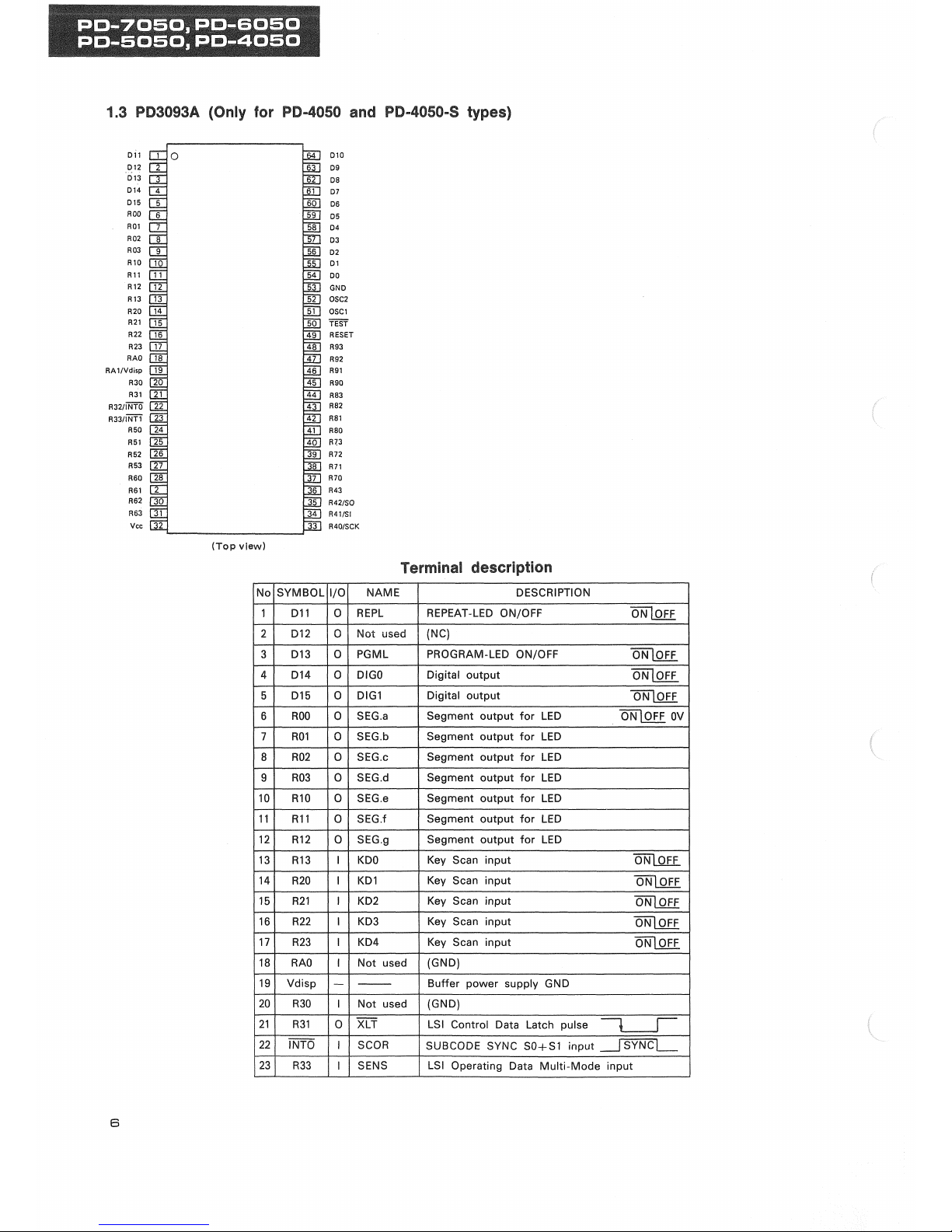
1.3 PD3093A (Only for PD-4050 and PD-4050-S types)
Terminal description
No
1
2
3
4
5
6
7
8
9
10
11
12
13
14
15
16
17
18
19
20
21
22
23
SYMBOL
D11
D12
D13
D14
D15
R00
R01
R02
R03
R10
R11
R12
R13
R20
R21
R22
R23
RAO
Vdisp
R30
R31
INTO
R33
I/O
0
0
0
0
0
0
0
0
0
0
0
0
I
I
I
I
I
I
-
I
0
I
I
NAME
REPL
Not used
PGML
DIGO
DIG1
SEG.a
SEG.b
SEG.c
SEG.d
SEG.e
SEG.f
SEG.g
KDO
KD1
KD2
KD3
KD4
Not used
Not used
XEJ
SCOR
SENS
DESCRIPTION I
REPEAT-LED ON/OFF
QNIQFF
(NC)
PROGRAM-LED ON/OFF "QNIQFF
Digital output QNIQFF 1
Digital output ON 10FF
Segment output for LED ON|OFF OV
1
Segment output for LED
Segment output for LED
Segment output for LED
Segment output for LED
Segment output for LED
Segment output for LED
Key Scan input ONlOFF
Key Scan input
"QNIQFF
Key Scan input ONlOFF
Key Scan input QNlOPF
Key Scan input ONlOFF
(GND)
Buffer power supply GND
(GND)
LSI Control Data Latch pulse \ |
SUBCODE SYNC S0+S1 input ISYNCI
LSI Operating Data Multi-Mode input
6
No
24
2b
26
2/
28
29
30
31
32
33
34
3b
36
3/
38
39
40
41
42
43
44
45
46
47
48
49
50
51
52
53
54
55
56
57
58
59
60
61
62
63
64
SYMBOL
R50
R51
R52
R53
R60
R61
R62
R63
VCC
SCK
SI
SO
R43
R70
R71
R72
R73
R80
R81
R82
R83
R90
R91
R92
piT™"
1
Reset
TEST
OSC1
OSC2
GND
DO
D1
D2
D3
D4
D5
D6
D7
D8
D9
D10
I/O
I
I
I
I
0
0
0
0
-
0
I
0
I
0
0
0
0
0
0
0
0
I
I
I
I
-
-
I
0
s
I
I
I
I
I
I
0
0
0
0
NAME
CRCF
GFS
Not used
FOK
LDON
MUTE
DEMP
Not used
CLK
SUBQ
DATA
TEST
Not used
Not used
Not used
Not used
Not used
Not used
LIN
LOUT
OHEN
CLMP
TNSD
Not used
Ms
RKD5
RKD4
RKD3
RKD2
RKD1
RKDO
Not used
Not used
PLYL
PASL
DESCRIPTION I
SUBCORD
Q-CRC
Result input NOfOK 1
Frame Sync Lock input NGlLOCK
(GND)
Focus OK input NG|OK
Laser Diode ON/OFF output QNlOFF 1
Muting output ON [OFF
De-emphasis ON/OFF output ON [OFF' 1
(NC)
+5V
Serial clock "UlflilT
SUBCODE Q Data Serial input T1 1 1 1 1
LSI Control Data Serial output [o]T72~|T
TJi
TEST Mode Select input TEST 1 NORMAL
(NC)
(NC)
(NC)
(NC)
(NC) |
(NC)
Disc Tray Loading [TFT
IN/OUT output BRAKE [OUT
Disc Tray OPENed SW input OPEN [NOT
Disc CLAMPed SW input CLAMPjNOT
Slider Inside SW input INSIDE [NOT
(GND)
CPU Reset input ResetlRUN
+ 5V
Clock Circuit input
(Internal Clock Circuit output)
GND
Remote-Control Key Strobe input IN ["OFF"
Remote-Control Key Code input (MSB)
Remote-Control Key Code input (MSB)
Remote-Control Key Code input (MSB)
Remote-Control Key Code input (MSB)
Remote-Control Key Code input (MSB)
Remote-Control Key Code input (LSB)
(NC)
(NC)
DLAY-LED ON/OFF
[QN!
5V
OV
PAUSE-LED ON/OFF
|5N|
5V
QV

2.
OPTICAL !WH IN THE PICK-UP
24 OPTICAL PATH AND OPTICAL PARTS 2-2 FEATURE OF EACH PART
DISC
Half mirror
Objective lens
Reflecting mirror
Grating (diffraction grating)
Laser diode
Photo diode (with pre-amplifier)
Fig.
2-1
shows the configuration of
this pick-up's optical part
The wavelength of the light emitted from the laser diode is
between 780 and 790 nm. The light is barely visible. This
light source is spread into an ellipse from an ultra-small
emission point. The light expands at a set angle.
The emitted light goes through a grating and is divided into
three beams of 0 step and ±1 step.
The other beams of ±2, 3, and n steps are also present, but
are lost and not used. When the light reaches the half
mirror, 50% is reflected. The remaining light permeates the
half mirror and is lost.
The light then goes to the reflecting mirror where all the
light is reflected to the objective lens (finite type).
Since this pick-up's objective lens uses a finite system
(finite because the LD's convergence distance is finite), a
collimator lens is unnecessary. The old models objective
lenses are called infinite type. The light that is converged on
an ultra-small diameter spot by these objective lenses is
reflected by the disc and returns to the objective lens. Then
it goes through the half mirror where 50% of it returns to
the laser diode. The remaining 50% of light goes through
and reaches the photo diode.
This has been a general outline of the optical path. The
features of each part are explained in the following section.
+1 order
0 order
(A)
-1 order
Fig.
2-2
(B)
(1) Laser diode (LD)
The size of previously-used LDs was 90. However, a newlydeveloped LD with a size of 5.60 has been introduced. This
has resulted in a compact and lightweight optical path.
(2) Objective lens
The collimator lens has been replaced by the finite objective lens which has a finite convergence distance for the
LD's optical path. This has resulted in lower costs while
preserving high performance.
The finite objective lens, like the conventional infinite lens,
is a high-performance lens designed to attain sufficient optical performance even when the optical parts are not
parallel within the optical path.
(3) Half mirror
The light that returns to the objective lens goes through the
half mirror. Since the half mirror is a glass plate, it is known
that astigmatism is created for the light which enters at an
angle. The old model similarly used a glass plate and had a
device in its optical part to cancel this astigmatism.
Whereas, this new pick-up uses the astigmatism advantageously for the focus servo.
Consequently, the multi-lens used in previous models has
not been incorporated in this new pick-up. This has resulted
in lower costs while preserving high performance. At the
same time, the points of parts have been reduced, improving dispersion and reliablity.
(4) Axle-sliding actuator
The position accuracy of the objective lens is an important
factor for the optical pick-up. The pick-up has a sliding axle
for the actuator which drives the objective lens. Accurate
and stable positioning of the objective lens is thus attained,
resulting in stable trackability. Also, a smooth frequency
response with low resonance is also realized as with the conventional spring-supported type.
8

(5) Resin body
The CD body has been made with computer-simulated
technology. To keep body changes to a minimum, resin has
been incorporated. Due to the mounting, materials were
carefully selected and the same reliability as the previouslyused aluminum has been realized.
The use of resin has made possible mounting configurations
that were not possible with aluminum. Therefore the use of
adhesives has been greatly reduced for improved reliability.
2-3 RF and servo signal
Fig.
2-3
(2) RF and servo signals
The beam, which has been reduced to an extremely
small spot by the objective lens, now strikes the disc side
on which the signal
is.
located. Part of the beam is then
reflected back to the objective lens and photo diode. A diagram showing how this beam is reflected off the disc is
shown in figure 2-2. (A) shows what happens when the concentrated beam is directed at a pit. Normally, this reflected
light would disrupt the output light beam. In the laser diodes
used in CD players, however, noise is reduced instead, resulting in stable performance. This property is very advantageous
for.the half prism which allows only half of the light energy
to pass.
A pit and (B) shows the same beam when reflected from
a space between pits. In case (A), the beam is diffracted, so
the dark part of the beam does not return to the objective
lens.
Instead, only the center of the beam passes through the
objective lens and reaches the photo diode. In case
(B),
there
is no diffraction because the beam does not strike a
pit.
There-
fore,
the entire beam is reflected back to the photo diode,
producing brighter beam than when a pit is reached. In this
system, the data on the disc, which is represented by pits,
is covered into an electrical signal at the photo diode according to the intensity (brightness) of the reflected^beam. The
RF signal is then produced from this electrical signal by the
computation circuit.
Fig. 2-3 shows how the focus signal is detected. (1) is
when the beam from the laser diode is accurately focused on
the disc by the objective lens. (2)shows what happens when
the disc comes closer to the pickup and (3) shows what happens when the disc moves farther away. The grating and concave lens, which have no direct effect on the focusing are not
shown in the diagram.
In case (1), the beam emanating from point
01
is reflected and diffracted on the disc surface to produce the condensed beam (02). In case (2), the beam is directed at a
point farther than that of beam 02. Fig. 2-4 shows the
properties of the half mirror. 1 through 7 shows the shape
of the beam at each point. Between points 2 and 6, which
are in a straight line, the beam is circular at point 4. Point 6
corresponds to beam 02 of fig. 2-3. If we assume that fig.
24 shows mode (1) of fig. 2-3, that means the beam is circular because the photo diode is located at point 4. In
mode (2) of fig. 2-3, the location of the photo diode is
closer to the cylindrical lens than it was in fig. 2-4. That
means the shape of the beam is the same as that of point 3
(an ellipse that has a longer width than height). In mode (3)
of fig. 2-3, the shape of the beam is that of point 5, an
ellipse that has a longer height than width.
Fig.
2-4 Half mirror
These beam shapes are shown in fig. 2-3. By performing a (A + C) — (B + D) computation using the A-D photo
diode quartering elements, the focus signal is produced.
Let's consider what happens as the objective lens is
gradually moved closer to the disc. If the objective is fairly far from the disc, only a small amount of light will be
returned to the photo diode. Furthermore, since the returning light is quartered, the focus signal would be 0.
If the objective lens is moved closer to the disc until
point 7 of fig. 24 is reached, the shape of the beam at the
photo diode becomes an ellipse that is higher than it is wide.
9
 Loading...