

Page 1

Service
Manual
PORTABLE CD-ROM DRIVE
PCP-PR24
THIS MANUAL IS APPLICABLE TO THE FOLLOWING MODEL(S) AND TYPE(S).
Type
KU ‡ DC power supply
Model
PCP-PR24
Power Requirement
Remarks
ORDER NO.
RRV1915
CONTENTS
1. SAFETY INFORMATION....................................2
2. EXPLODED VIEWS AND PARTS LIST .............3
3. SCHEMATIC DIAGRAM..................................... 7
4. PCB CONNECTION DIAGRAM .......................16
5. PCB PARTS LIST.............................................18
6. ADJUSTMENT.................................................. 20
PIONEER ELECTRONIC CORPORATION 4-1, Meguro 1-Chome, Meguro-ku, Tokyo 153-8654, Japan
PIONEER ELECTRONICS SERVICE, INC. P.O. Box 1760, Long Beach, CA 90801-1760, U.S.A.
PIONEER ELECTRONIC (EUROPE) N.V . Haven 1087, Keetberglaan 1, 9120 Melsele, Belgium
PIONEER ELECTRONICS ASIACENTRE PTE. LTD. 501 Orchard Road, #10-00 Lane Crawford Place, Singapore 0923
CC
C PIONEER ELECTRONIC CORPORATION 1998
CC
7. GENERAL INFORMATION .............................. 26
7.1 PARTS ....................................................... 26
7.1.1 IC ............................................................. 26
7.1.2 DISPLAY..................................................32
7.2 BLOCK DIAGRAM....................................... 32
8. PANEL FACILITIES AND SPECIFICATIONS
...................................................................33
T-ZZR FEB.1998 Printed in Japan
Page 2
PCP-PR24
1. SAFETY INFORMATION
This service manual is intended for qualified service technicians; it is not meant for the casual
do-it-yourselfer. Qualified technicians have the necessary test equipment and tools, and have been
trained to properly and safely repair complex products such as those covered by this manual.
Improperly performed repairs can adversely affect the safety and reliability of the product and may
void the warranty. If you are not qualified to perform the repair of this product properly and safely, you
should not risk trying to do so and refer the repair to a qualified service technician.
WARNING
Lead in solder used in this product is listed by the California Health and Welfare agency as a known reproductive toxicant which
may cause birth defects or other reproductive harm (California Health & Safety Code, Section 25249.5).
When servicing or handling circuit boards and other components which contain lead in solder, avoid unprotected skin contact with
the solder. Also, when soldering do not inhale any smoke or fumes produced.
NOTICE
(FOR CANADIAN MODEL ONLY)
Fuse symbols (fast operating fuse) and/or (slow operating fuse) on PCB indicate that replacement parts
must be of identical designation.
REMARQUE
(POUR MODÈLE CANADIEN SEULEMENT)
Les symboles de fusible (fusible de type rapide) et/ou (fusible de type lent) sur CCI indiquent que les
pièces de remplacement doivent avoir la même désignation.
(FOR USA MODEL ONLY)
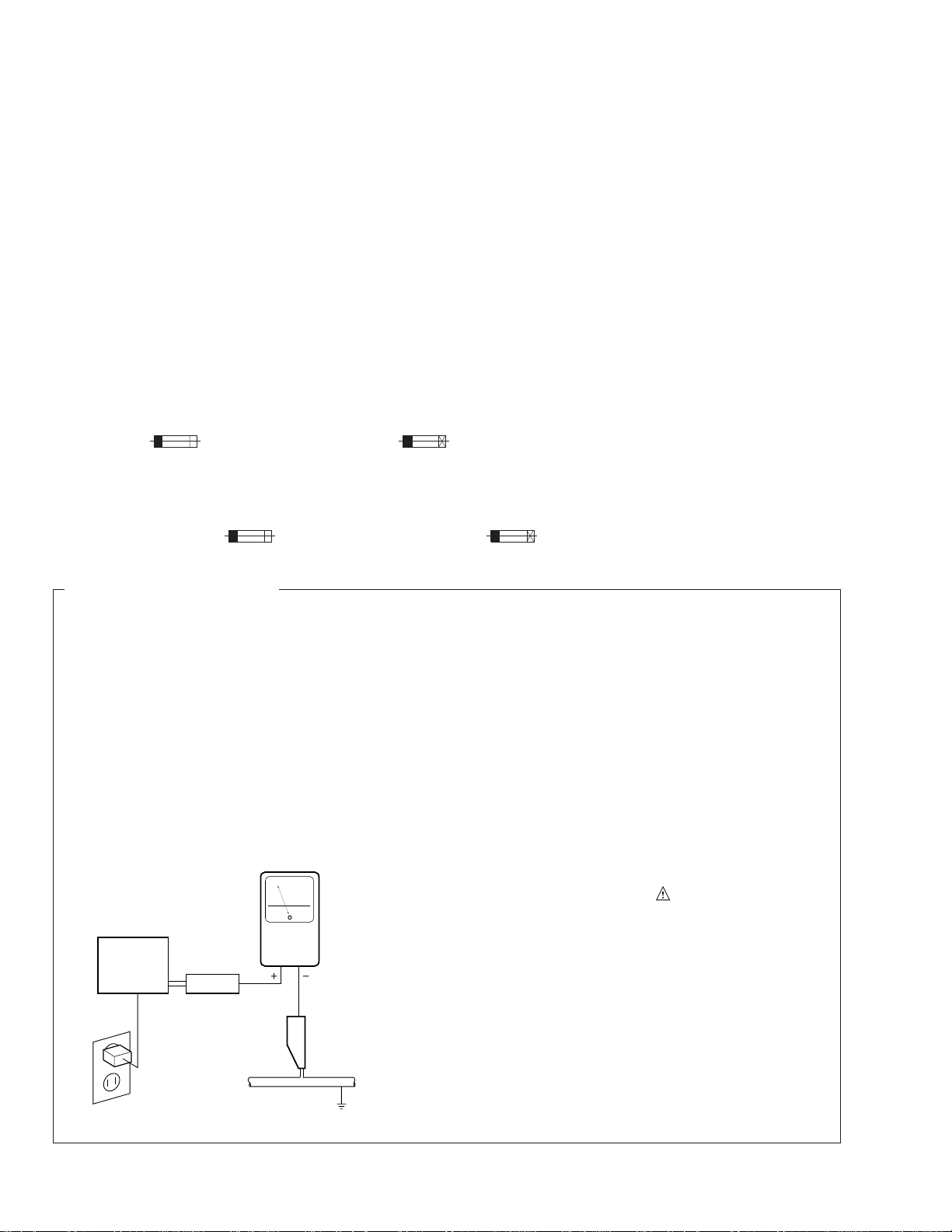
1. SAFETY PRECAUTIONS
The following check should be performed for the
continued protection of the customer and service
technician.
LEAKAGE CURRENT CHECK
Measure leakage current to a known earth ground
(water pipe, conduit, etc.) by connecting a leakage
current tester such as Simpson Model 229-2 or
equivalent between the earth ground and all exposed
metal parts of the appliance (input/output terminals,
screwheads, metal overlays, control shaft, etc.). Plug
the AC line cord of the appliance directly into a 120V
AC 60 Hz outlet and turn the AC power switch on. Any
current measured must not exceed 0.5 mA.
Reading should
not be above
0.5 mA
Earth ground
Device
under
test
Also test with plug
reversed
(Using AC adapter
plug as required)
Leakage
current
tester
Test all exposed
metal surfaces
AC Leakage Test
ANY MEASUREMENTS NOT WITHIN THE LIMITS
OUTLINED ABOVE ARE INDICATIVE OF A POTENTIAL SHOCK HAZARD AND MUST BE CORRECTED BEFORE RETURNING THE APPLIANCE
TO THE CUSTOMER.
2. PRODUCT SAFETY NOTICE
Many electrical and mechanical parts in the appliance have special safety related characteristics. These
are often not evident from visual inspection nor the
protection afforded by them necessarily can be obtained by using replacement components rated for
voltage, wattage , etc. Replacement parts which have
these special safety characteristics are identified in
this Service Manual.
Electrical components having such features are
identified by marking with a
on the parts list in this Service Manual.
The use of a substitute replacement component which
does not have the same safety characteristics as the
PIONEER recommended replacement one, shown in
the parts list in this Service Manual, may create shock,
fire, or other hazards.
Product Safety is continuously under review and
new instructions are issued from time to time. For
the latest information, always consult the current
PIONEER Service Manual. A subscription to, or additional copies of, PIONEER Service Manual may be
obtained at a nominal charge from PIONEER.
on the schematics and
2
Page 3
PCP-PR24
PCP-PR24
Front
15
11
(x10)
13
7
12
9
8
16
17
10
1
4
5
6
2
14
3
2. EXPLOLDED VIEWS AND PARTS LIST
NOTES : ÷ Parts marked by “ NSP ” are generally unavailable because they are not in our Master Spare Parts List.
÷ The mark found on some component parts indicates the importance of the safety factor of the part.
Therefore, when replacing, be sure to use parts of identical designation.
÷ Screw adjacent to ∞ mark on the product are used for disassembly.
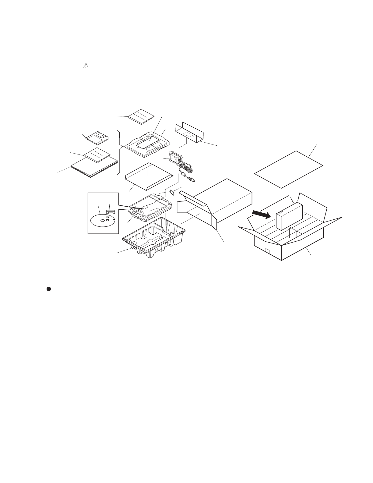
2.1 PACKING
Parts List
Mark No. Description Parts No.
1 MIRROR MAT SHEET DHL1050
(400 X 550 X 0.5 )
2 PARTITION QHA1029
3 PARTITION PLATE(590X370) QHA1026
4 TRAY QHA1028
5 PACKING CASE QHG1049
NSP 9 SILICA GEL (2g) QEN1002
6 MASTER CARTON QHG1050
7 POLYETHYLENE BAG Z21-038
(230 X 340 X 0.03 )
8 PARTITION S QHA1030
Mark No. Description Parts No.
10 OPERATING INSTRUCTIONS QRB1004
NSP 11 WARRANTY CARD QRY1002
NSP 17 PACKING SEAL DHX1005
(English)
12 AC ADAPTOR QWX1067
13 SETUP DISK QWX1070
14 TRANSPORT PAD QHA1021
15 TRANSPORT SPACER QEE1001
16 LICENCE AGREEMENT CARD QRM1007
3
Page 4
PCP-PR24
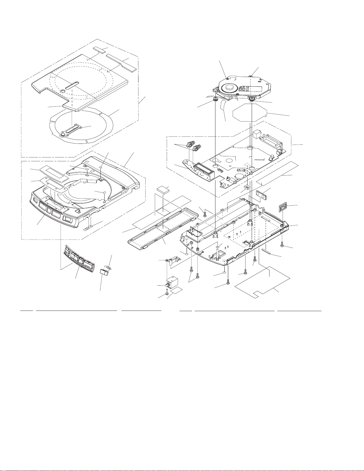
2.2 EXTERIOR
23
24
39
29
38
22
Refer to " 2.3 SERVO MECHANISM
ASSY SECTION ".
3
8
2
8
8
33
18
21
30
26
26
26
19
20
37(1/2)
6
15
16
Mark No. Description Parts No.
1 MOTHER BOARD ASSY QWM1036
2 FLEXIBLE CORD QDD1003
3 SERVO MECHANISM ASSY QXX1014
4 PLUNGER QXP1001
5 BATTERY TERMINAL A QBH1005
10
11
5
1
28
34
27
31
27
35
27
27
14
31
4
32
27
7
12
37(2/2)
25
36
17
13
27
Mark No. Description Parts No.
NSP 21 LCD WINDOW QNK1046
22 TOP COVER ASSY QXA1025
NSP 23 TOP COVER QNK1065
NSP 24 TC WINDOW QNK1047
25 MOTHER BOARD ASSY QXX1015
6 OPEN SPRING QBH1004
7 BATTERY TERMINAL B QBK1004
8 FLOAT RUBBER QEB1020
9 ..................
10 LOCK LEVER QNK1077
11 PLUNGER KNOB QNK1071
12 LEG RUBBER QEB1035
13 CHASSIS QNK1066
14 BATTERY COVER QNK1061
15 BUTTON ASSY QNK1057
16 OPEN KNOB QNK1058
17 POWER BUTTON QNK1041
18 BODY ASSY QXA1021
19 COVER SPRING QBK1003
NSP 20 BODY QNK1067
4
26 DISC PAD QED1008
27 SCREW PPZ20P060FZK
28 CUSHION QEB1022
29 TOP COVER SHEET QED1009
NSP 30 LCD SHEET QEC1018
31 LEG RUBBER F QE1034
NSP 32 DOUBLE FACE TAPE QEN1003
NSP 33 SHIELD SHEET QEC1021
NSP 34 DIP SHIELD QNH1026
35 WASHER WA31D054D025
36 65 LABEL DRW1659
NSP 37 TYPE NAME LABEL QRW1078
38 TOP COVER PAD A QEB1032
39 TOP COVER PAD B QEB1033
Page 5
2.3 SERVO MECHANISM ASSY
11
3
13
10
3
PCP-PR24
Mark No. Description Parts No.
6
3
NSP 1 PICKUP ASSY QWY1002
NSP 11 TOP PLATE SHEET QEC1025
7
5
2 SCREW ( 1.7 X 4 ) ABA7022
3 SCREW ( B 1.7X 5 ) DBA1098
4 EARTH RUG ASSY DDX1161
5 GUIDE SHAFT DLA1785
6 TOP PLATE DNH2222
7 MECHA FRAME QNK1076
8 SCREW GUIDE S DNK3345
9 SPINDLE MOTOR QXM1004
10 STEPPING MOTOR DXM1088
12 PU FLEXIBLE CORD QNP1012
13 EARTH SPRING DBH1359
3
9
3
8
2
3
4
To open the top cover without drive power
from the AC adapter or batteries:
Slide the emergency opening switch on the bottom of the
unit to open the top cover.
1
12
NOTE!
Without drive power from the AC adapter or
from batteries, the top cover of this unit can
not be opened.
Do not force the top cover open while the disc
is spinning.
To realize a high transfer rate, the disc in this unit
spins at high speed.
If the top cover is opened while the disc is spinning,
the disc may be thrown out. So, do not open the
top cover while the disc is spinning.
5
Page 6

PCP-PR24
6
Page 7
1
23
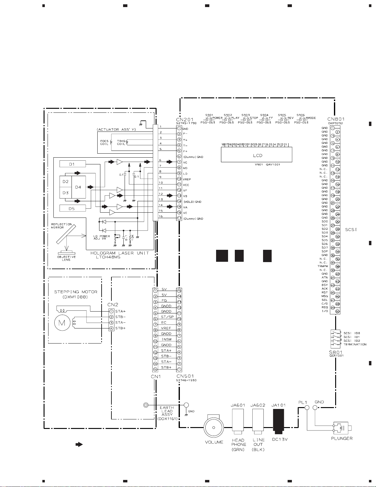
3. SCHEMATIC DIAGRAM
4
PCP-PR24
Note: When ordering service parts, be sure to refer to "EXPLODED VIEWS
AND PARTS LIST" or "PCB PARTS LIST".
3.1 OVERALL SCHEMATIC DIAGRAM
PICKUP ASSY
(QWY1002)
10K
A
B
SERVO MECHA ASSY
(QXX1014)
(DXM1004)
SPINDLE MOTOR
A
( A
1/3
–
MOTHER BOARD ASSY
(QWM1036)
VR651
A
3/3
)
C
8
7
6
5
D
:RF and AUDIO SIGNAL ROUTE
1
7
2
3
4
Page 8
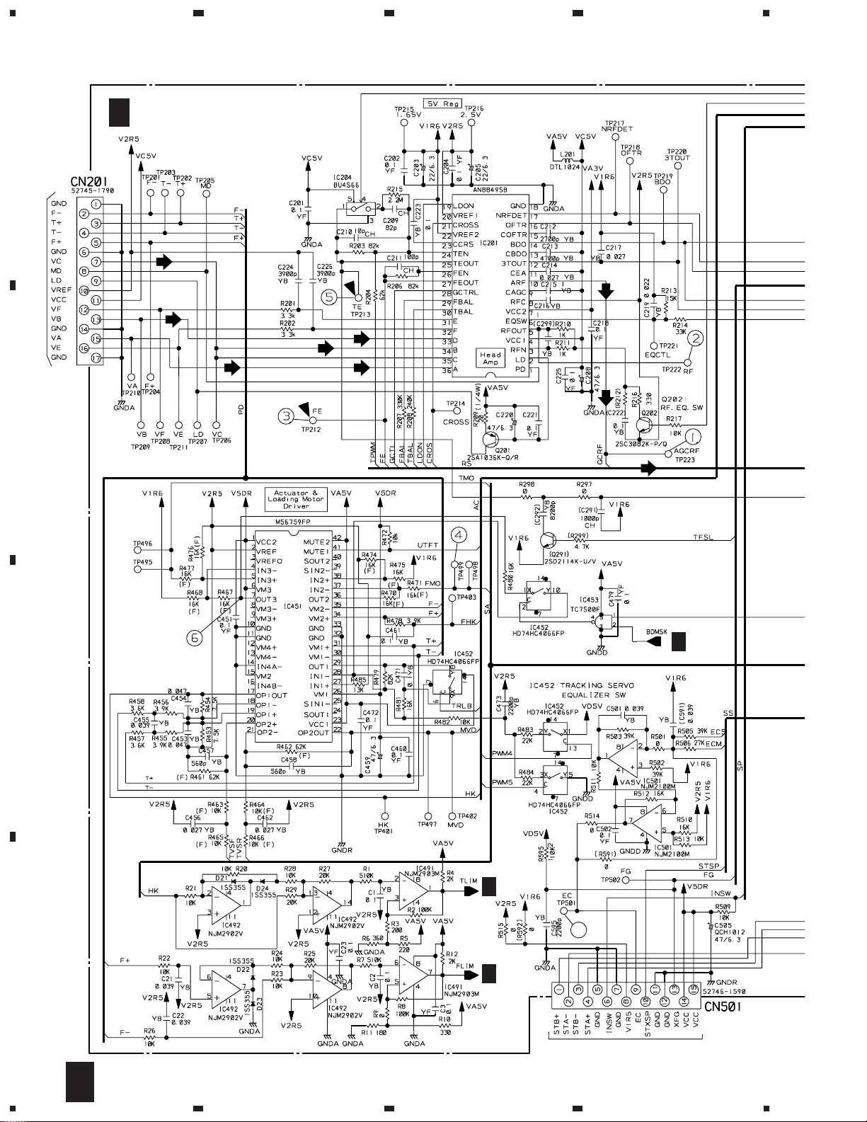
1
234
PCP-PR24
3.2 MOTHER BOARD ASSY (1/3)
A
To PICKUP ASSY
B
A 1/3
MOTHER BOARD ASSY (1/3)
(QWM1036)
A 2/3
C
A 2/3
7
(Tantalum)
D
A 2/3
To CN1 SPINDLE MOTOR and
STEPPING MOTOR
8
A 1/3
1234
Page 9
A
5
2/3
67
PCP-PR24
SIGNAL ROUTE
: RF SIGNAL ROUTE
: AUDIO SIGNAL ROUTE
8
A
A
2/3
B
C
A
3/3
(Tantalum)
Headphone
Out
Line Out
D
A 1/3
5
6
7
8
9
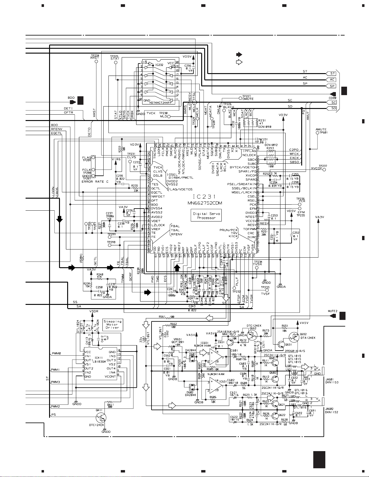
Page 10
1
234
PCP-PR24
3.3 MOTHER BOARD ASSY (2/3)
Correct
A
A
A
1/3
B
MOTHER BOARD ASSY (2/3) (QWM1036)
2/3
A
3/3
A
1/3
C
D
10
A 2/3
1234
Page 11
5
67
8
PCP-PR24
A
(Tantalum)
B
2.84V
2.84V
2.84V
5
2.84V
2.84V
2.84V
2.84V
2.84V
2.84V
2.84V
2.84V
2.84V
2.84V
2.84V
2.84V
2.84V
6
2.84V
2.84V
2.84V
4.75V
C
D
A 2/3
7
8
11
Page 12

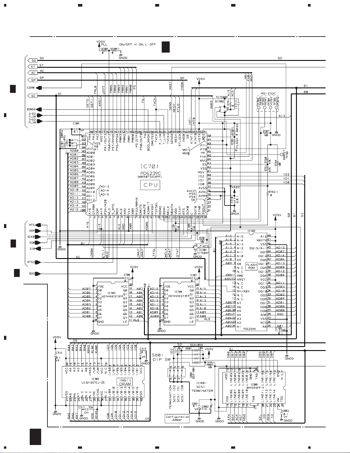
1
234
PCP-PR24
3.4 MOTHER BOARD ASSY (3/3)
A
B
A
MOTHER BOARD ASSY (3/3) (QWM1036)
3/3
MISRO-COMPUTER
POWER.SUPPLY
ALKALI
2.5V
C
8
9
D
12
A 3/3
1234
Page 13

5
67
8
PCP-PR24
A
To PLUNGER
5V
B
2/3
11
A
A
1/3
13
12
10
S901: POWER SW
S902:
S903: CHG
S904:
S905:
S906: MODE
S907: OPEN
S908: BATTERY PACK DETECT
S909: OPEN/CLOSE
C
D
HOLDER
A 3/3
5
6
7
8
13
Page 14

PCP-PR24
Waveforms (MOTHER BOARD ASSY)
Note: The encircled numbers denote measuring point in the schematic diagram.
3
1
AGC RF – TP223
0.2V/div., 0.5 µS/div.
× 1 PLAY
1
AGC RF – TP223
0.2V/div., 20 nS/div.
× 24 PLAY
– 1.65V
– 1.65V
CH1: FE – TP212
0.5V/div., 50 mS/div.
4
CH2: FMO – TP499
0.5V/div., 50 mS/div.
FOCUS IN
5
CH1: TE – TP213
0.5V/div., 2 mS/div.
6
CH2: T DRV
2V/div., 2 mS/div.
MULTI TRACK
JUMP
3
4
5
6
GND
–
(CH1)
GND
–
(CH2)
– 0V
2
RF – TP222
0.2V/div., 0.5 µS/div.
× 1 PLAY
2
RF – TP222
0.2V/div., 20 nS/div.
× 24 PLAY
3
CH1: FE – TP212
0.5V/div., 20 mS/div.
4
CH2: FMO – TP499
0.5V/div., 20 mS/div.
3
– 2.1V
– 2.1V
7
EC – TP501
0.5V/div., 10 mS/div.
× 24 PLAY
8
Q124-Collector
5V/div., 2 µS/div.
V5D and A System
9
Q123-Collector
5V/div., 2 µS/div.
V5DR System
– 0V
– 0V
14
FOCUS IN
4
–
–
GND
(CH1)
GND
(CH2)
– 0V
Page 15

0
IC901-Pin 100 (SI0)
1V/div., 20 mS/div.
-
IC901-Pin 5 (RTS)
1V/div., 20 mS/div.
– 0V
– 0V
=
IC901-Pin 73 (SEG)
1V/div., 5 mS/div.
~
IC901-Pin 51 (COM)
1V/div., 5 mS/div.
PCP-PR24
– 0V
– 0V
IC201 (AN8849SB)
10
11
12
13
14
15
16
17
18
19
20
21
22
27
28
29
30
31
36
1
2
3
4
5
6
7
8
9
|
|
Voltage [ V ]
0
4.6
2.5
5
2.5
1.4
3.5
2.5
3.2
1.9
3
1.8
3.6
0
3.6
0
4.9
0
0
2.5
2.2
1.8
0.9
1.8
1.8
2.5
Pin No.
IC451 (M56759FP)
1
2
3
4
5
6
7
8
9
10
11
12
13
14
Voltage [ V ]
12.4
2.5
0.3
1.2
2.1
12.4
0.6
0.3
0.1
0
0
0.1
0.1
0.2
Pin No.
Pin No.
15
16
17
18
19
20
22 0
22
23
24
25
26
27
Voltage [ V ]
12.4
0.2
0.6
0.6
1.5
0.6
0
5
0
0
5
2.5
Pin No.
28
|
31
32
33
34
35
36
37
38
39
40
41
42
Voltage [ V ]
0.6
0
0
0.2
0.2
0.8
1.3
2.1
0
0
5
3.7
15
Page 16

1
PCP-PR24
234
4. PCB CONNECTION DIAGRAM
A
MOTHER BOARD ASSY
SIDE A
A
IC141
IC142
Q102
Q110
Q498
Q499
Q109
Q107
Q106
VR651
B
IC452
To CN1
SPINDLE MOTOR and
STEPPING MOTOR
IC491
IC501
IC453
To PICKUP ASSY
C
NOTE FOR PCB DIAGRAMS:
1. Part numbers in PCB diagrams match those in the schematic
diagrams.
2. A comparison between the main parts of PCB and schematic
diagrams is shown below.
Symbol in PCB
Diagrams
BCE
BCE
Q122
Q125
IC801
DGS
3. The parts mounted on this PCB include all necessary parts
for several destination.
For further information for respective destinations, be sure
to check with the schematic diagram.
4. Viewpoint of PCB diagrams
D
Symbol in Schematic
Diagrams
BCE
BCE
BCEBCE
DGSDGS
CapacitorConnector
Part Name
Transistor
Transistor
with resistor
Field effect
transistor
Resistor array
3-terminal
regulator
SIDE A
16
P. C. Board Chip Part
SIDE B
QNP1011-B
This is a 4-layer circuit board. Mainly Vcc and GND are wired in the intermediate layers.
A
1234
Page 17

MOTHER B ASSY
A
Q112
Q111
Q104
Q105
Q108
Q103
Q141
1
IC111
IC451
23
PCP-PR24
SIDE B
4
A
IC492
Q662
Q411
Q661
Q652
Q602
Q651
Q601
IC411
IC651
Q622
B
Q621
IC231
IC232
Q124
Q291
IC701
IC201
IC204
IC705
IC706
IC301
Q201
IC703
IC704
IC702
IC302
C
IC121
1
Q123
IC802
D
QNP1011-B
A
2
3
4
17
Page 18

PCP-PR24
5. PCB PARTS LIST
NOTES : ÷ Parts marked by “ NSP ” are generally unavailable because they are not in our Master Spare Parts List.
÷ The
÷ When ordering resistors, first convert resistance values into code form as shown in the following examples.
A
MOTHER BOARD ASSY
SEMICONDUCTORS
IC121 AN8011S
IC201 AN8849SB
IC801 BH9595FP-Y
IC204 BU4S66
IC452 HD74HC4066FP
IC232 HD74HCT244FP
IC802 ICP-S1.0
IC411 LB1836M
IC302 LC321667CJ-25
IC301 LC895126-LF4L
IC451 M56759FP
IC231 MN662752CDM
IC501 NJM2100M
IC492 NJM2902V
IC491 NJM2903M
IC651 NJM3414AM
IC901 PD4945A
IC701 PD6239C
IC702 PD6254C
IC181 PQ7VZ5
IC142 PST9145N
IC111 S-80750AN-JE
IC141 S-81250SG-QD
IC703, IC704 TC74VHC573F
IC453 TC7S00F
IC705 TC7S04F
Q651 2PD601A
Q201, Q661 2SA1036K
Q109, Q123, Q124 2SA1834
Q499 2SA1797
Q102, Q103, Q106 2SB1197K
Q601, Q602, Q621, Q622 2SC2411K
Q141 2SC2412K
Q202 2SC3082K
Q497 2SC4672
mark found on some component parts indicates the importance of the safety factor of the part.
Therefore, when replacing, be sure to use parts of identical designation.
Ex. 1 When there are 2 effective digits (any digit apart from 0), such as 560 ohm and 47k ohm (tolerance is shown by
J = 5%, and K = 10%).
1
560 Ω = 56 × 10
47k Ω = 47 × 10
= 561................................................... RD1/4PU 5 6 1 J
3
= 473 .................................................. RD1/4PU 4 7 3 J
0.5 Ω = R50 ...................................................................... RN2H Â 5 0 K
1 Ω = 1R0 ......................................................................... RS1P 1 Â 0 K
Ex. 2 When there are 3 effective digits (such as in high precision metal film resistors).
1
5.62k Ω = 562 × 10
= 5621 ........................................... RN1/4PC 5 6 2 1 F
Mark No. Description Parts No.Mark No. Description Parts No.
Q652 DTA124EK
Q104, Q105, Q107, Q108 DTC124EK
Q110- Q112, Q411, Q498, Q662 DTC124EK
D101, D103, D105 1SR154-400
D21- D24, D499, D901 1SS355
D601, D602 DA204K
D104 RB050L-40
D121, D122, D142, D801 RB160L-40
D102 UDZ2.0B
COILS AND FILTERS
L201, L411 (4.7 µH) DTL1024
F101, F121, F123, F124(EMI FILTER) QTF1025
L121, L122 (47 µH) QTL1012
L601, L602, L651( Chip beads ) QTL1015
L603, L604, L691( Chip beads) QTL1016
L661, L662 (Chip coils 22 µH ) VTL1067
SWITCHES AND RELAYS
S901-S906 PSG-063
S907, S908 QSG1002
S909 QSG1003
S801 QSX1001
CAPACITORS
C210 CCSRCH100D50
C211 CCSRCH101J50
C128 CCSRCH271J50
C317 CCSRCH330J50
C133, C136 CCSRCH331J50
C623, C624 CCSRCH471J50
C209 CCSRCH820J50
C621, C622 CEV100M16
C123, C124, C601, C602 CEV101M10
C185, C413, C655 CEV101M6R3
C203, C205 CEV220M6R3
C144, C208, C220, C459, C802 CEV470M6R3
Q122, Q125 2SD1615
18
Page 19

PCP-PR24
Mark No. Description Parts No. Mark No. Description Parts No.
C215, C216 CKSQYB105K10
C247, C255, C258 CKSQYB154K16
C245 CKSQYB474K16
C113, C232, C240, C241 CKSRYB102K50
C112, C125, C129, C661, C662 CKSRYB103K50
C1, C2, C223, C238, C251 CKSRYB104K16
C306, C461, C471, C603, C604 CKSRYB104K16
C473, C595 CKSRYB222K50
C219, C235, C239, C242, C243 CKSRYB223K25
C250 CKSRYB223K25
C212 CKSRYB272K50
C214, C217, C456, C462 CKSRYB273K16
C224, C226, C237 CKSRYB392K50
C21, C22, C248, C254, C455 CKSRYB393K16
C501 CKSRYB393K16
C213 CKSRYB472K50
C453, C454 CKSRYB473K16
C457, C458 CKSRYB561K50
C142, C143 CKSRYF103Z50
C102, C111, C122, C126, C130 CKSRYF104Z25
C181, C182, C201, C202, C204 CKSRYF104Z25
C218, C221, C225, C23, C231 CKSRYF104Z25
C233, C236, C249, C252,C253 CKSRYF104Z25
C256, C3, C315, C316, C412 CKSRYF104Z25
C451, C460, C472, C479, C502 CKSRYF104Z25
C651- C653, C691, C692, C701 CKSRYF104Z25
C705- C710, C801, C803 CKSRYF104Z25
C901, C902 CKSRYF104Z25
R162 RS1/16S2702F
R461, R462 RS1/16S6202F
R121, R131 RS1/16S6801F
R112 RS1/16S7502F
R127, R270 RS1/2S271J
R104 RS1/4S100J
R101 RS1/4S120J
R209 RS1/4S200J
R114, R117 RS1S750J
VR651 (10 kΩ) QCP1001
Other Resistors RS1/16S J
OTHERS
CN201 FX CONNECTOR 52745-1790
CN501 FX CONNECTOR 52746-1590
JA602 MINI JACK DKN1152
JA601 MINI JACK DKN1153
JA101 DCIN JACK DKN1154
CN801 L Type DIP CONNECTOR50 DKP3292
V901 L.C.D. QAV1001
X901 (CSTCC4.0 MHz) DSS1088
X701 (CSTCV20.0 MHz) DSS1095
X301 (CSTCV33.86 MHz) QSS1012
LCD HOLDER QNK1045
C301, C304, C305, C307-C314 CKSRYF105Z10
C127 (330 µF/16V) QCH1007
C101, C134, C135 (10 µF/16V) QCH1010
C131 (220 µF/10V) QCH1011
C505, C671 (47 µF/6.3V) QCH1012
C121, C132 (220 µF/25V) QCH1014
RESISTORS
R231(47 Ω × 4) DCN1090
R312(56 Ω × 4) DCN1091
R253, R301, R313-R317(100 Ω × 4) DCN1092
R306, R307, R801(10 kΩ × 4) DCN1094
R102 RS1/10S560J
R499 RS1/10S201J
R497 RS1/10S241J
R183 RS1/16S1001F
R463- R466 RS1/16S1002F
R121, R132 RS1/16S1201F
R136 RS1/16S1202F
R113 RS1/16S1203F
R467, R468, R470, R471 RS1/16S1602F
R474- R477 RS1/16S1602F
R181 RS1/16S1801F
R924 RS1/16S2002F
R111, R991 RS1/16S2402F
19
Page 20

PCP-PR24
6. ADJUSTMENT
6.1 PREPARATIONS
6.1.1 Jigs and Measuring Instruments
CD TEST DISC
(CDT-304)
Low-frequency
oscillator
Precise
screwdriver
Dual-trace
oscilloscope
(10 : 1 probe)
6.1.2 Necessary Adjustment Points
When Adjustment points
Exchange
MOTHER BOARD ASSY
screwdriver
(large)
Service remote
controller
(RU-V101)
1.2.3. Page 24, 25
screwdriver
(small)
Interface
screwdriver
(medium)
External adder
amplifier
Exchange
SERVO MECH ASSY
20
1.2.3. Page 24, 25
Page 21

PCP-PR24
6.2 ADJUSTMENT
6.2.1 How to Start/Cancel Test Mode
SERVICE REMOTE CONTROLLER
Function of the Remoto Controller (RU-V101) for Service
÷ Test Mode
When operating the CD-ROM directly,it is possible to operate by connecting the RU-V101 to the CD-ROM with the interface.
Schematic Diagram of the Conversion Jig for Remote Control Operation
RU-V101
Interface
1
2
3
3P mini jack
Q1: DTC124ES or UN4212
TEST MODE : ON
2.2k
10k
Q1
IC231
GNDD
V +5V
1
REMI
2
3
GND
4
PH type
connector
(4P)
VD5V
REMI
SIDE B
IC701
MOTHER BOARD ASSY
LCD Display
BUSY
2
Power Switch: ON
1
MODE Button, 4 Button, ¢ Button Same time push
TRACK MIN
SEC
21
Page 22

PCP-PR24
Function Table of the Remote Controller (RU-V101) for Service
RU-V101
REJECT : Spindle stop
PAUSE : Pause
PLAY : Play (Trace)
STILL/STEP E : Test command
STILL/STEP e :
MULTI-SPEED + : Test command
MULTI-SPEED - :
SCAN ¡ : No entry
SCAN 1 : No entry
CLEAR : Clear
FRAME : Block set
TIME : Time set
CHAPTER : Track set
SEARCH : Search
10 key : Numerical input
DISPLAY (FUNC + 1) : No entry
STILL (FUNC + 2) : No entry
C-MODE (FUNC + 3) : No entry
VIDEO (FUNC + 4) : No entry
STOP. M (FUNC + 5) : No entry
START (FUNC + 6) : Start
AUDIO (FUNC + 7) : No entry
SPEED (FUNC + 8) : No entry
Test command
Test command
Test Command
Key Operation Command Description
[0] + [TIME] {0TM} All servo OFF
[1] + [TIME] {1TM} Laser - diode (LD) ON
[2] + [TIME] {2TM} Focus ON/OFF
[3] + [TIME] {3TM} Spindle ON
[4] + [TIME] {4TM} Tracking ON/OFF
[5] + [TIME] {5TM} PLL ON/OFF
[6] + [TIME] {6TM} Focus Up/Down
[8] + [TIME] {8TM} Spindle rotation control : X1 CLV
[9] + [TIME] {9TM} Spindle rotation control : H1 Mode
[STILL/STEP >>] {SF} 1 Track jump : FWD
[STILL/STEP <<] {SR} 1 Track jump : REV
*
] + [*] + [*] + [MULTI-SPEED +] {
[
[
*
] + [*] + [*] + [MULTI-SPEED -] {
***
***
MF}
MR}
***
Track jump : FWD
***
Track jump : REV
22
Page 23

6.2.2 Adjustment Locations
PCP-PR24
MOTHER BOARD ASSY
FE
TE
V1R6
V2R5
SIDE B
VA
GND
VC
VB
LD POWER ADJ. VR
23
Page 24

PCP-PR24
6.2.3 Check and Adjustment
1. Focus Offset Check
PLAY MODE
TEST DISC
PLAY
START
V1R6
FE
GND
MOTHER BOARD ASSY
Focus Error Offset
and
Tracking Error Offset
CD-ROM Player
Prove(10:1)
GND
GND
Prove(10:1)
(CH1)
(CH2)
V1R6
GND
FCS.ERR
GND
Oscilloscope
DC Mode
V: 500 mV/div
H: 10 mSec/div
A
B
2. Tracking Error Barance Check
¶ Test mode
Check
SPDL servo = CLOSE
FOCUS servo = CLOSE
TRKG servo = OPEN
TEST DISC
R=35mm
PLAY
CD-ROM Player
START
V1R6
TE
MOTHER BOARD ASSY
GND
A
C
B
Prove(10:1)
A≠B
V1R6
A=B
A
V1R6
B
Oscilloscope
DC Mode
V: 500 mV/div
H: 5 mSec/div
24
Page 25

3. RF Level Adjustment
¶ Test mode
TEST DISC
¶
PLAY
LD POWER
ADJ. VR
SERVO MECHA ASSY
PCP-PR24
330 mVP-P
±30 mV
START
MOTHER BOARD ASSY
VAV2R5GND VB VC
VC
+
–
VB
+
–
VA
+
–
4.7k
4.7k
4.7k
4.7k
CD-ROM Player
10p
4.7k
–
+
+
–
+5V
–5V
75
0.1µ
0.1µ
+
47/16
47/16
+
Oscilloscope
AC Mode
V: 100 mV/div
H: 1 µSec/div
Prove(10:1)
GND
25
Page 26

PCP-PR24
7. GENERAL INFORMATION
7.1 PARTS
7.1.1 IC
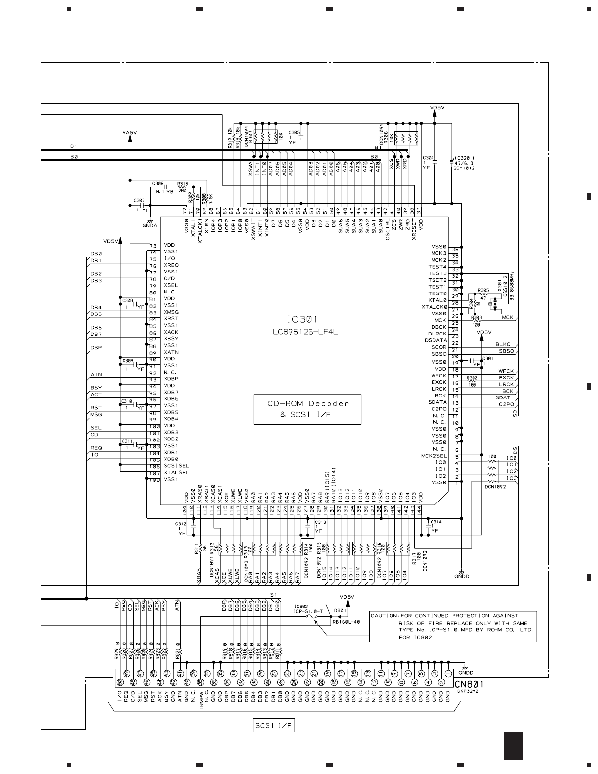
LC895126-LF4L (IC301: MOTHER BOARD ASSY)
CD-ROM DECODER and SCSI I/F
Block Diagram
EXCK
CD-DSP
HOST
ZINT0, 1
Micro
controller
ZSWAIT
XTALCK
XTAL
MCK
∗1
∗2
∗3
∗4
∗5
∗6
CD-DSP I/F
&
SYNC
Detector
Each
Block
Register
Decoder
Clock
Generator
Data bus (0:7)
Each
Block
RAM Data bus (0:15)
Sub-code I/F
de-interleave
Address generator
Sub-code ECC
Address generator
De-scramble &
Buffering
Address generator
ECC & EDC
Address generator
SCSI I/F Block
Data output input I/F
Address generator
Microcontroller
RAM access
Address generator
CAV Audio control
Address generator
LC895126-LF4L
Address bus (0:21)
The information shown in the list is basic information and
may not correspond exactly to that shown in the
schematic diagrams.
∗
1: WFCK, SBSO, SCOR
∗
2: BCK, SDATA, LRCK, C2PO
∗
3: DB0~DB7, DBP, BSY, MSG, SEL,
RST, REQ, I/O, C/D
∗
4: ACK, ATN
∗
5: ZRD, ZWR, SUA0~SUA6, ZCS, CSCTRL
∗
6: D0~D7
∗
7: IO0~IO15
∗
8: RA0~RA10,ZRAS0, ZRAS1, ZCAS0,
ZCAS1, ZOE, ZUWE, ZLWE
∗
9: DBCK, DLRCK, DSDATA
Note: IO14, IO15 and RA9, RA10 are
∗7
∗8
∗9
same pins.
External
Buffer
DRAM
DAC
Each Block
Bus control
signal
Bus
Arbiter
&
RAM
Controller
Pin Function
No. Pin Name I/O Pin Function
1 Vss0 - Logic GND
2 IO2 To Buffer RAM
I I I/O Data input / output
4 IO0 With pull-up resistors
built-in
5 MCK2SEL I At PLL ,switches
MCK2 (22MHz,20MHz)&
MCK3 (27MHz, 25MHz).
Connected to VDD.
6 NC - OPEN
7
I Vss0 - Logic GND
9
10 NC -
OPEN
11 NC -
26
No. Pin Name I/O Pin Function
12 C2PO I
13 SDATA I
CD-DSP I/F
14 BCK I
15 LRCK I
16 EXCK O
SUB CODE input/output
17 WFCK I
18 VDD- +5V (Digital) power supply
19 Vss0 - Logic GND
20 SBSO I
SUB CODE input/output
21 SCOR I
22 DSDATA O DAC output
No. Pin Name I/O Pin Function
23 DLRCK O
DAC output
24 DBCK O
25 MCK O XTALCK1 1/1 & 1/2
STOP out put
26 Vss0 - Logic GND
27 XTALCK0 I X'tal oscillation input
28 XTAL0 O X'tal oscillation output
29 TEST0
I I I TEST terminals
33TEST4 Connected to Vss0.
34 MCK2 - XTALCK0 1/1,1/2 &
1/512 STOP output
Page 27

PCP-PR24
No. Pin Name I/O Description
35 MCK3 - XTALCK0 1/1, 2/5 &
1/512 STOP output
36 Vss0 - Logic GND
37 VDD- +5V (Digital) power supply
38 ZRESET I LSI reset, 0 : Reset
39 ZRD I MC (Microcontroller)
Data read SIG. input
40 ZWR I MC (Microcontroller)
Data writing SIG. output
41 ZCS I MC (Microcontroller)
register-chip select signal
input
42 CSCTRL I MC (Microcontroller)
CS active Lo/Hi selection
43 SUA0 MC (Microcontroller)
I I I Register select signal
49 SUA6
50 D0 MC (Microcontroller)
I I I/O DATA signal
53 D3
54 VDD- +5V (Digital) power supply
55 Vss0 - Logic GND
56 D4 MC (Microcontroller)
I I I/O DATA Signal
59 D7
60 ZINT0 O MC (Microcontroller)
Interrupt request SIG output
( ECC : Set by the register.)
61 ZINT1 O MC (Microcontroller)
Interrupt request SIG output
(SCSI : Set by the register.)
62 ZSWAIT O WAIT signal to
MC (Microcontroller)
63 Vss0 - Logic GND
64 IOP0
I I I/O Universal input/output
68 IOP4
69 X1EN I Without PLL : Fixed at 0.
With PLL : Connected to
VDD through the resistor.
70 XTALCK1 I Shock-proof oscillation
input For PLL built-in : PLL
71 XTAL1 O Shock-proof oscillation
output For PLL built-in : PLL
72 Vss0 - PLL built-in : Analog Vss
73 VDD - PLL built-in : Analog VDD
No. Pin Name I/O Description
74 Vss1 - GND for SCSI I/F driver
75 I/O I/O
76 REQ I/O
77 Vss1 - GND for SCSI I/F driver
78 C/D I/O
79 SEL I/O
80 NC - OPEN
81 VDD - +5V (Digital) power supply
82 Vss1 - GND for SCSI I/F driver
83 MSG I/O
84 RST I/O
85 Vss1 - GND for SCSI I/F driver
86 ACK I/O
87 BSY I/O
88 Vss1 - GND for SCSI I/F driver
89 ATN I/O SCSI Terminal
90 VDD - +5V (Digital) power supply
91 Vss1 - GND for SCSI I/F driver
92 NC - OPEN
93 DBP I/O SCSI Terminal
94 VDD - +5V (Digital) power supply
95 DB7 I/O
96 DB6 I/O
97 Vss1 - GND for SCSI I/F driver
98 DB5 I/O
99 DB4 I/O
100 VDD - +5V (Digital) power supply
101 DB3 I/O
102 DB2 I/O
103 Vss1 - GND for SCSI I/F driver
104 DB1 I/O
105 DB0 I/O
SCSI Terminal
SCSI Terminal
SCSI Terminal
SCSI Terminal
SCSI Terminal
SCSI Terminal
SCSI Terminal
SCSI Terminal
No. Pin Name I/O Description
106 SCSISELI SCSI terminal allocat select
terminal (Vss0: Unchanged)
107 XTALSEL I PLL,XTALoscillation select
108 Vss1 - GND for SCSI I/F driver
109 VDD - +5V (Digital) power supply
110 Vss0 - Logic GND
111 ZRAS0 O RAS signal output
terminal-0 to Buffer RAM
(Normal : Terminal"0"used.)
112 ZRAS1 O RAS signal output terminal
-1 to Buffer RAM
113 ZCAS0 O CAS signal output terminal
- 0 to Buffer RAM
(Normal : Terminal"0"used.)
114 ZCAS1 O CAS signal output terminal
- 1 to Buffer RAM
115 ZOE O Buffer RAM
Output Enable
116 ZUWE O Buffer RAM
Upper Write Enable
117 ZLWE O Buffer RAM
Lower Write Enable
118 Vss0 - Logic GND
119 RA0 Address signal output
I I O to Buffer RAM
125 RA6
126 VDD - +5V (Digital) power supply
127 Vss0 - Logic GND
128 RA7 - Address signal output
to Buffer RAM
129 RA8 -
130 RA9 (IO15) - Address signal output
& data input/output
131 RA10 to Buffer RAM
(IO14) (pull-up resistors built-in)
132 IO13 Data input/output
I I to Buffer RAM
137 IO8 (pull-up resistors built-in)
138 Vss0 - Logic GND
139 IO7 Data input/output
I I to Buffer RAM
143 IO3 (pull-up resistors built-in)
144 VDD - +5V (Digital) power supply
The initial letter "Z" of the terminal names
indicates that their signals are of negative
logic.
27
Page 28

PCP-PR24
MN662752CDM (IC231: MOTHER BOARD ASSY)
Digital Servo Processor
Block Diagram
VCC
DVDD1
DVDD2
DVDD3
IOSEL
CLVS
CRC
BLKCK
NCLDCK
SBCK
SUBC
RESY
BCLKIN/SSEL
SQCK
SUBQ
AVSS2
AVDD2
DSLB
PCK
EFM
PLLFPO
PLLF
PLLFNO
PLLF2
DSLF
IREF
IREF2
DRF
QRF
ARF
RSEL
SRDATAIN/PSEL
GCTL
EQCTL
MLD
MCLK
MDATA
XVCOF
VCOF
VDETOH/BYTCK
SMCK
FCLK
PMCK
CSEL
LRCKIN/MSEL
STAT
PWCTL/DIRBK
TVSR
TVSF
TVCK
83
4
28
85
26
31
80
20
99
98
97
82
91
11
10
41
42
32
87
86
62
63
66
64
61
56
57
59
60
58
88
92
35
36
16
15
12
94
65
96
21
23
22
89
90
6
X2
5
X1
13
27
75
74
30
DIGITAL
DEEMPHASIS
BUFFER
SUB CODE
DSL · PLL VCO
EQUALIZER
CONTROL
VCO
TIMING
GENERATOR
PITCH
CONTROL
TRV
SPEED
DEMODULATION
INTERPOLATION
DEMODULATION
4 TIMES OVER
SAMPLING
DIGITAL FILTER
16 k
SRAM
EFM
SYNC
SUB CODE
PWM PWM
MICROCOMPUTER
INTERFACE
A/D
CONVERTER
CIRC ERROR
CORRECTION
DEINTER
LEAVE
SERVO
CPU
INPUT PORT
1 bit DAC
PWM
(R)
PWM LOGIC
PWM
(L)
DIGITAL
AUDIO
INTERFACE
SERVO
INTER POLATION
SOFT MUTING
DIGITAL
ATTENUATION
CONVERTER
OUTPUT
PORT
SERVO TIMING
GENERATOR
CLV
CAV
D/A
OUTR
69
70
AVSS1
68
AVDD1
67
OUTL
33
FLAG/VDETOS
100
IPFLAG
8
TX
95
SPARI/FG
73
ECM
72
PC
2
LRCK
3
SRDATA
1
BCLK
9
DMUTE
81
TOFPWM
77
TRV
76
KICK
45
VREF
54
ECS
53
TVD1
52
TRD
51
FOD
49
TBAL
48
FBAL
55
TVD2
34
TES
NTLOCK/NWVEL
18
19
NFLOCK/NQVEL
24
LDON
14
SENSE/PLAY
93
SPARO
78
PRUN/PCX
79
DIRC
28
7 29 71 40
DVSS1
DVSS2
DVSS3
DVSS4
47 46 50 44
FE
TE
RFENV
LZLOCK
25 43 39
VDET
TRCRS
BDO
17
NRST
37 38
NRFDAT
OFT
84
NTEST
Page 29

Pin Function
PCP-PR24
No. Pin Name I/O Description
1 BCLK O SRDATA bit clock output
2 LRCK O L / R check signal output H : Lch audio data
3 SRDATA O Serial data output
4 DVDD1 I Power supply for oscillation circuit
5 X1 I X' tal oscillation circuit input
6 X2 O X' tal oscillation circuit out f=33.8688/16.9344MHz
7 DVSS1 I GND for oscillation circuit
8 TX O Digital audio interface output
9 DMUTE I Muting input H : mute
10 SUBQ O Subcode "Q" data output
11 SQCK I Subcode "Q" register external clock input
12 MDATA I Microcomputer command data input
13 STAT O Status signal (CRC, CLVS, TTSTOP, FCLV,
14 SENCE/ O Sence signal output (OFT , FESL , NACEND,
NAJEND,SFG,NWTEND) or PLAY signal output
PLAY ( at command input ,common for NWVEL &
NQVEL output commands )
15 MCLK I Microcomputer command clock signal input
16 MLD I Microcomputer command load signal input L: Load
17 NRST I Reset input L: Reset
18 NTLOCK/ O Tracking servo lead-in signal (L: Lead-in) or
NW VEL multiple-speed play signal output (at command
19 NFLOCK/ O Focus servo lead-in signal (L: Lead-in) or X4-speed
NQVEL play signal output ( at command input, common
20 BLKCK O Subcode block clock signal
21 SMCK O MSEL=H 8.4672MHz Clock signal output
22 PMCK O 88.2kHz Clock signal output
23 FCLK O X' tal frame clock signal output
24 LDON O Laser ON signal output
25 TRCRS I Track cross signal input
26 IOSEL I Mode selection terminal
Direction detect output for external track count ,
27 DIRBK/ O 3-state output or universal PWM output
PWCTL ( at command input )
L : Rch audio data
f=33.8688/16.9344MHz
SQOK, FLAG6, SENSE, /FLOCK, /TLOCK)
( At leading edge , latches the data. )
input, common for PLAY & NQVEL out commands
for PLAY & NWVEL output commands )
fBLKCK=75kHz
MSEL=L 16.9344MHz Clock signal output
( fFCLK=7.35kHz at normal Play mode )
No. Pin Name I/O Description
28 DVDD2 I Power supply for digital circuit.
29 DVSS2 I GND for digital circuit
30 TVCK O Pulse output for external track count
31 CLVS O Spindle servo phase-sync signal output
H : CLV , L : Rough servo
32 DSLB O Data slice balance compensation PWM output
33 FLAG/ O Flag signal output or software-vibration-detection
VDETOS monitor signal output ( at command input )
34 TES O Tracking error shunt signal output
H: Shunt
35 GCTL O PWM output for head-amp-gain control
36 EQCTL O PWM output for variable equalizer
37 NRFDET I RF detector signal input L: Detection
38 OFT I Off track H: Off track
39 BDO I Dropout signal input H: Dropout
40 DVSS4 I GND for digital circuit
41 AVSS2 I GND for analog circuit
( DSL, PLL, DA output & AD )
42 AVDD2 I Power supply for analog circuit
( DSL, PLL, DA output & AD )
43 VDET I Vibration detection signal input , comparator input
44 LZLOCK I Test input Normal : VREF
45 VREF I Reference voltage for DA output ( ECS, TRD,
FOD, FBAL, TBAL, TVD1 & TVD2 )
46 TE I Tracking error signal input ( analog input )
47 FE I Focus error signal input ( analog input )
48 FBAL O Focus balance adjustment output
49 TBAL O Tracking balance adjustment output
50 RFENV I RF envelop signal input ( analog input )
51 FOD O Focus drive output
52 TRD O Tracking drive output
53 TVD1 O Traverse drive output
54 ECS O Spindle motor drive signal
( Servo error signal output )
55 TVD2 O Test output Normal : OPEN
56 IREF I Reference current input terminal
57 IREF2 I Reference current switching signal input.
58 ARF I RF signal input
29
Page 30

PCP-PR24
MN662752CDM
No. Pin Nam I/O Description
59 DRF I
DSL time constant selection terminal
60 QRF I
61 DSLF I/O DSL loop filter terminal
62 PLFPO I/O PLLF charge pump output (H )
63 PLLF I/O PLL loop filter terminal
64 PLLF2 I/O PLL loop filter selector terminal
65 VCOF I/O VCO loop filter terminal
66 PLFNO I/O PLLF charge pump output ( L )
67 OUTL O L ch audio output
68 AVDD1 I Power supply for analog circuit
[ for Lch/Rch audio output block ]
69 OUTR O R ch audio output
70 AVSS1 I GND for analog circuit
[ for Lch/Rch audio output block ]
71 DVSS3 I GND for digital circuit
72 PC O Spindle motor ON output L: ON
73 ECM O Spindle motor drive signal (forced mode output)
3-state
74 TVSF O Traverse speed control output (in outer) 3-state
75 TVSR O Traverse speed control output (in inner) 3-state
76 KICK O Kick pulse output 3-state
77 TRV O Traverse forced-forwarding output 3-state
78 PRUN/ O Pickup track crossing detection output
PCX or spindle driver control output
( at command input )
79 DIRC O Pickup track crossing direction detect output
80 CRC O Subcode CRC check result output
H : OK , L : NG
81 TOFPWM O PWM output for external tracking offset adjustment
82 RESY O IOSEL=H :
Frame-sync re-syc signal RESY output
H: Sync L : OUT of sync
IOSEL=L :
Address reset signal for error correction
de-interleave RAM , FLAG6 output
L: generates address reset .
83 VCC5V I +5V power supply
84 NTEST I Test terminal Normally : H
85 DVDD3 I Power supply for digital circuit
86 EFM O EFM signal output
IOSEL=H : EFM signal output
IOSEL=L : 16.9344MHz clock output
No. Pin Name I/O Description
87 PCK O PLL extract clock output
fPCK=4.3218MHz (at normal play mode)
88 RSEL I RF signal polarity selection terminal
When the positive level is H : RSEL=H
When the positive level is L : RSEL=L
89 CSEL I X' tal oscillation frequency selection terminal
(External oscillation frequency 33.8688MHz : H)
(External oscillation frequency 16.9344MHz : L )
90 MSEL/ I IOSEL=H :
LRCKIN SMCK terminal output, frequency selector terminal
H: SMCK=8.4672MHz
L: SMCK=16.9344MHz
IOSEL=L : LRCK input
H: L ch data , L: R ch data
( SMCK terminal output =16.9344MHz )
91 SSEL/ I IOSEL=H :
BCLKIN SUBQ terminal output mode-selector terminal
H : "Q" code buffer mode
IOSEL=L : BCLK input
H: L ch data , L: R ch data
( SUBQ terminal output mode = "Q" code
buffer mode )
92 PSEL/ I IOSEL=H : Test terminal
SRDATAIN IOSEL=L : SRDATA input ( Normally : L )
93 SPARO O Aux. output terminal
94 XVCOF I/O VCO loop filter terminal Not used : L
95 SPARI/ I FG signal input terminal for spindle CAV servo
FG
96 BYTCK/ O IOSEL=H : Byte clock signal output
VDETOH IOSEL=L : Traverse STOP signal output
, or hardware vibration detection monitor signal
output ( at command input )
97 SUBC O Subcode serial output
98 SBCK I Clock input 2 for subcode serial output
99 NCLDCK O Subcode frame clock output terminal
fCLDCK=7.35 kHz
100 IPFLAG O Interpolation flag signal output H:Interpolation
30
Page 31

AN8849SB (IC201: MOTHER BOARD ASSY)
Head Amp.
Block Diagram
RFN
RFOUT
3 5 6 8 9 10 17 11 12
EQOUT
RFC
CAGC
ARF
NRFDET
CEA
PCP-PR24
3TOUT
Pin Function
ADD AMP
36A
35
C
34
B
33
D
32
F
31
E
ADD
AMP
ADD
AMP
AMP
AMP
GND
EQ
GCA BCA
GCA BCA
VCC1
VCC2
GCA BCA
GCA BCA
AMP
30 25 2418 4 7 23 21 29 28 19
TBAL
TEOUT
No. Pin Name Description
1 PD APC. Amp input terminal
2 LD APC. Amp output terminal
3 RFN RF adder Amp reverse input terminal
4 VCC1 Power supply terminal 1
5 RFOUT RF adder Amp output terminal
6 EQOUT EQ characteristics control terminal
7 VCC2 Power supply terminal 2
8 RFC AGC input HPF capacity connector terminal
9 CAGC AGC loop filter connector terminal
10 ARF AGC output terminal
11 CEA HPF-Amp capacity connector terminal
12 3TOUT 3TENV output terminal
13 CBDO RF negative-side envelope detection connector terminal
14 BDO BDO output terminal
15
COFTR
RF positive-side envelope detection connector terminal
16 OFTR OFTR output terminal
17 NRFDET NRFDET output terminal
18 GND Ground GND
ENV DET.
RF AGC
BDO
RFDET
AC
OFTR
AMP
–
+
–
+
–
+
TEN
COMP
CCRS
CROSS
FBAL
GCTRL
LDON
No. Pin Name Description
19 LDON APC & masking control terminal
20 VREF1 VREF1 output terminal
21 CROSS CROSS output terminal
22 VREF2 VREF2 output terminal
23 CCRS CROSS capacity connector terminal
24 TEN TE. Amp reverse input terminal
25 TEOUT TE. Amp output terminal
26 FEN FE. Amp reverse input terminal
27 FEOUT FE. Amp output terminal
28 GCTRL GCTRL terminal
29 FBAL FBAL control terminal
30 TBAL TBAL control terminal
31 E Tracking signal input terminal 1
32 F Tracking signal input terminal 2
33 D Focus signal input terminal 4
34 B Focus signal input terminal 2
35 C Focus signal input terminal 3
36 A Focus signal input terminal 1
13 CBDO
BDO
14
COFTR
15
16
OFTR
26
FEN
27
FEOUT
VREF2
22
VREF1
20
2
LD
1
PD
31
Page 32

PCP-PR24
7.1.2 Display
QAV1001 (V901: MOTHER BOARD ASSY)
LCD
BUSY
TRACK MIN
Display Status
A-CD-ROM lights up During disc confirmation
CD-ROM, PowerAccess or PowerRead During CD-ROM playback
SEC
P-ON Power ON by pressing POWER and PLAY key for at least 2 seconds
no-disc No disc
A-CD, 00-00:00 During playback of an audio/CD Extra disc
P-OFF Power OFF by pressing POWER
When the battery is exhausted
open lights up When the top cover OPEN button is pressed
(Audio/CD Extra disc) During repeat of all titles
(Audio/CD Extra disc) During repeat of one title
RANDOM (Audio/CD Extra disc) During random play
BUSY During data exchange with the personal computer
7.2 BLOCK DIAGRAM
32
Page 33

8. PANEL FACILITIES AND SPECIFICATIONS
PANEL FACILITIES
Front and Side
=
9 Skip / Scan button (reverse direction)
1
When this button is pressed during playback of a music CD,
the pickup skips back to the beginning of the track and
playback of that track starts again. When this button is held
down, the track is played at high speed in reverse direction.
PCP-PR24
2
3
0
9
8
7
6
4
5
1 Power switch ( )
When this switch is pressed for at least 1 sec, the power is
switched ON/OFF ” ” will flash on the display for
several seconds.
2 Line output terminal (LINE OUT)
The music CD signal is put out. Connect to powered speakers
or to a stereo amplifier.
3 Headphone volume control
This is used to adjust the sound volume for the headphone
terminal.
4 Headphone terminal
This is a stereo minijack for connection of headphones.
5 Open button
When this is slid to the right, the top cover opens after the
disc stop spinning.
6 Play/Pause button
This is used for playback of music CDs. When a music CD is
inserted and this button is pressed, playback status is
reached, and when the button is pressed in playback status,
pause status is reached.
7 Stop button
When this button is pressed once during playback of a music
CD, the playback will stop.
10 MODE button
The playback mode changes when the MODE button is
pressed. The playback indicator display also changes
accordingly.
<CD-ROM playback>
[High-speed mode:
The data transfer rate on the maximum will be 24x speed.
This mode is selected when the power is switched on
with use of the AC adapter. When the vibrations or the
spinning noises appear large, press the MODE button
once to switch to the PS mode shown below.
[PS mode: -
The data transfer rate is equivalent to 4.4x speed at the
innermost part of the disc and equivalent to 10x speed
at the outermost part of the disc. This mode is selected
when the power is switched on with use of alkali batteries
or nicad batteries.
<Music CD playback>
[Normal playback: No display]
This mode is selected when the power is switched on.
Playback stops after the last track playback is completed.
[All tracks repeat: P ]
After the last track playback is completed, playback starts
again from the first track.
[One track repeat: P1]
The track presently being played will be repeated.
[Random playback: RANDOM]
The tracks will be played in random sequence. Playback
stops after all tracks are played.
[Random repeat: P RANDOM]
Playback continues in random sequence.
11 LCD panel
]
]
8 Skip / Scan button (forward direction)
When this button is pressed during playback of a music CD,
the pickup skips to the start of the next track and the next
track is played back. When this button is held down, the track
is played at high speed.
12 Top cover
33
Page 34

PCP-PR24
Rear and Bottom
$
#
@
13 Emergency open switch
14 SCSI ID/SCSI terminator switch
OFF
DIP SWITCH SETTINGS
1
2 3 4
ON
TERMINATION ON/OFF
OFF
OFF
ONONON
OFF
SCSI ID
ON
OFF OFF
OFF OFF
ON
0
1234567
OFF OFF
OFF
OFF
OFF
ON
ON
ON
ON
!
ON
ON
ON
~
LCD panel
123
5
6
4
1 Disc indicator
A-CD-ROM (flashing): Indicates identification of the disc
A-CD: Indicates that a music CD has been
CD-ROM: Indicates that a CD-ROM has been
2 Playback indicator
P: All-track repeat playback mode.
P1: One-track repeat playback mode.
RANDOM: Random playback mode.
PRANDOM: Random repeat playback mode.
3 Busy indicator
This flashes during data access.
4 Playback information/Operation mode
indicator
Playback information: Displayed at the time of playback of
A
type.
inserted.
inserted.
a music CD.
15 SCSI connector
Connect the interface cable. factory default setting
16 Power supply terminal
Use the accessory AC adapter for connection to a wall
receptacle.
Never use any other AC adapter.
17 Battery cover
34
Track No. Elapsed playback time
Operation mode:
:
This flashes for several seconds when the power is
switched on.
: This flashes for several seconds when the power is
switched off.
: This indicates that no disc has been inserted.
: This lights when the top cover is open.
:
This lights at the time of CD-ROM playback in
high-speed mode.
: This lights at the time of CD-ROM playback in
PS mode.
5 Battery voltage drop indicator
This lights when the battery power has run down.
Page 35

SPECIFICATIONS
7 General
Usable discs.........................................................................
CD-ROM discs (conforming to the Yellow Book)
(only for 8 cm/12 cm discs) .................................................
CD music CD (conforming to the Red Book)
Data transfer speed ............... 1560 - 3670 kB/S (HI Mode)
670 - 1545 kB/S (PS Mode)
Interface..................................................................... SCSI2
Data buffer........................................................ 128 k Bytes
Average access time ................................................. 90 m s
Average seek time..................................................... 70 ms
7 Audio output
Frequency characteristic ............ 17 Hz to 20 kHz + 0.1dB
S/N ratio ........................................................ 80 dB or more
Distortion .........................................................0.1% or less
Output level .......................... 0.7 V rms ±0.1 V (LINE OUT)
7 Accessories
Setup disk (3.5” floppy disk) .............................................1
AC adapter ......................................................................... 1
Operating instructions ....................................................... 1
Warranty card ....................................................................1
User contract agreement ...................................................1
PCP-PR24
7 Others
Power supply .......................................................................
Alkali batteries (AA/LR6) x 6 (commercial product)
Power consumption ............................................................
Battery life
Alkali batteries
Playback of music CDs............................ About 2 hours
CD-ROM playback................................. About 1.5 hour
External dimensions ...........132 (W) x 28 (H) x 203 (D) mm
Weight..................................................... 370 g (13-3/32 oz)
Operation temperature ........ +5°C to +35°C (41°F to 95°F)
Operation humidity ............... 5% to 85% (no condensation)
Storage temperature...... –40°C to +60°C (–40°F to 140°F)
Built-in terminator (ON/OFF switchable)
÷
The specifications and design subject to modification without
notice, due to improvements.
AC 120 V , 60 Hz (AC adapter )(accessory)
Size 3 Nicad batteries (1.2V 1000mAh)x6
About 11 W at the time of CD-ROM playback
(with use of the AC adapter (standby: 0.7 W)
(5-1/5 (W) x 1-3/32 (H) x 8 (D) in.)
Accessory Confirmation
÷ AC adapter x 1 (QWX1067)
÷ Operating instructions x 1
(QRB1004)
÷ Warranty card x 1
(QRY1002)
÷ User contract agreement x 1
(QRM1007)
÷ Setup disk x 1
(QWX1070 ) DOS/KU
35
 Loading...