

Page 1
ORDER NO.
CRT3058
PUB. NO. CRT3058
AUDIO SYSTEM
POWER AMPLIFIER
Manufactured for TOYOTA
by PIONEER CORPORATION
VEHICLE DESTINATION PRODUCED AFTER TOYOTA PART No. ID No. PIONEER MODEL No.
LEXUS LS430 Europe, Middle Near East, August 2003 86280-50320 GM-8537ZT/WL
Australia, North America 86280-50330 GM-8537ZT-91/WL
General Area
LS430
Page 2
2
1
234
12
34
F
E
D
C
B
A
GM-8537ZT/WL
SAFETY INFORMATION
This service manual is intended for qualified service technicians; it is not meant for the casual do-it-yourselfer.
Qualified technicians have the necessary test equipment and tools, and have been trained to properly and safely repair
complex products such as those covered by this manual.
Improperly performed repairs can adversely affect the safety and reliability of the product and may void the warranty.
If you are not qualified to perform the repair of this product properly and safely, you should not risk trying to do so
and refer the repair to a qualified service technician.
GM-8537ZT/WL
- Supplementally model is identical to the original except for the addition of following items.
*: Non Spare Part
Part No.
Description GM-8537ZT-91/WL
Cover CEG1045(x2)
Polyethylene Bag CEG1174
* Air Cap CHW1945
Carton CHG4796
Contain Box CHL5173(x1/2)
GM-8537ZT-91/WL
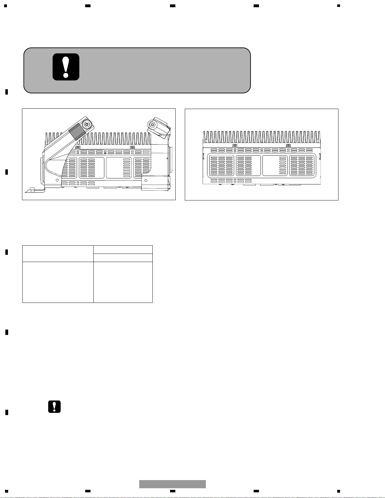
NOTE:
- When diagnosing a product, take care of its heated portion.
Power IC (IC701,711,721)
Power Supply IC (IC852,853)
DSP IC (IC301,311)
Heat Sink
IC Holder
For details, refer to "Important symbols for good services".
Page 3

3
5
6
7
8
F
E
D
C
B
A
5
6
7
8
GM-8537ZT/WL
[ Important symbols for good services ]
In this manual, the symbols shown-below indicate that adjustments, settings or cleaning should be made securely.
When you find the procedures bearing any of the symbols, be sure to fulfill them:
2. Adjustments
To keep the original performances of the product, optimum adjustments or specification confirmation is indispensable.
In accordance with the procedures or instructions described in this manual, adjustments should be performed.
3. Cleaning
For optical pickups, tape-deck heads, lenses and mirrors used in projection monitors, and other parts requiring cleaning,
proper cleaning should be performed to restore their performances.
5. Lubricants, glues, and replacement parts
Appropriately applying grease or glue can maintain the product performances. But improper lubrication or applying
glue may lead to failures or troubles in the product. By following the instructions in this manual, be sure to apply the
prescribed grease or glue to proper portions by the appropriate amount.For replacement parts or tools, the prescribed
ones should be used.
4. Shipping mode and shipping screws
To protect the product from damages or failures that may be caused during transit, the shipping mode should be set or
the shipping screws should be installed before shipping out in accordance with this manual, if necessary.
1. Product safety
You should conform to the regulations governing the product (safety, radio and noise, and other regulations), and
should keep the safety during servicing by following the safety instructions described in this manual.
CONTENTS
SAFETY INFORMATION ............................................2
1. SPECIFICATIONS .......................................................3
2. EXPLODED VIEWS AND PARTS LIST ......................4
2.1 EXTERIOR............................................................4
3. BLOCK DIAGRAM AND SCHEMATIC DIAGRAM ....6
3.1 BLOCK DIAGRAM ...............................................6
3.2 SCHEMATIC DIAGRAM(GUIDE PAGE)..............8
4. PCB CONNECTION DIAGRAM................................14
4.1 DSP UNIT...........................................................14
4.2 AMP UNIT..........................................................18
4.3 ASL UNIT...........................................................22
5. ELECTRICAL PARTS LIST........................................23
6. ADJUSTMENT.........................................................28
7. GENERAL INFORMATION.......................................35
7.1 DIAGNOSIS .......................................................35
7.1.1 DISASSEMBLY .........................................35
7.1.2
CONNECTOR FUNCTION DESCRIPTION ......37
7.1.3 THE METHOD OF DISTINGUISHING DEFECTIVE
DSP IC(IC301 OR IC311) DURING DSP ERROR .....38
7.2 IC ........................................................................40
7.3EXPLANATION...................................................44
7.3.1 SYSTEM BLOCK DIAGRAM.....................44
7.3.2 OPERATIONAL FLOW CHART .................47
8. OPERATIONS ...........................................................48
1. SPECIFICATIONS
Power source . . . . . . . . . . . . .13.2±0.1V(10.5-16.0V)
Grounding . . . . . . . . . . . . . . . .Negative type
Backup current . . . . . . . . . . . .0.3mA or less
Dimensions(No Bracket) . . . .285mm(W)x51mm(H)x128mm(D)
Weight(No Bracket) . . . . . . . .1.6kg
Maximum output power . . . .39W or more(Front)
13W or more(Tweeter)
21W or more(Rear)
35W or more(Woofer)
Page 4
4
1
234
12
34
F
E
D
C
B
A
GM-8537ZT/WL
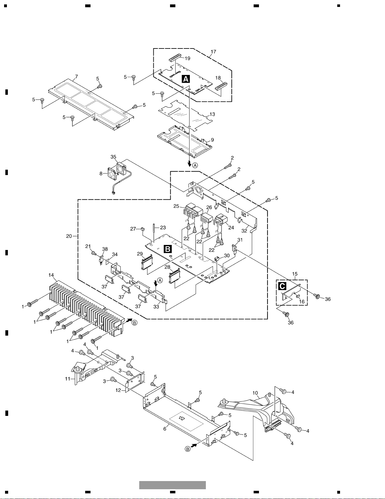
2. EXPLODED VIEWS AND PARTS LIST
2.1 EXTERIOR
Page 5

5
5
6
7
8
F
E
D
C
B
A
5
6
7
8
GM-8537ZT/WL
1 Screw AMZ30P220FTC
2 Screw BMZ26P140FTC
3 Screw (GM-8537ZT/WL) BMZ40P050FTC
4 Screw (GM-8537ZT/WL) BMZ50P060FTC
5 Screw BSZ26P060FTC
6 Chassis CNA2557
7 Case CNB2790
8 Holder CND1204
9 Shield Case CND1276
* 10 86285-50110 (GM-8537ZT/WL) CND1331
* 11 86286-50040 (GM-8537ZT/WL) CND1332
12 Bracket (GM-8537ZT/WL) CND1465
13 Insulator CNM7999
14 Heat Sink CNR1660
15 ASL Unit CWM8305
16 Connector(CN403) CKS4605
17 DSP Unit CWM8583
18 Socket(CN101) CKS4616
19 Socket(CN102) CKS4616
20 Amp Unit CWM8584
21 Screw BSZ26P080FTC
22 Screw(M3x6) CBA1393
23 Clamper CEF1034
24 Connector(CN903) CKM1064
25 Connector(CN901) CKM1363
26 Connector(CN902) CKM1364
27 Plug(CN801) CKS1036
28 Plug(CN905) CKS4569
29 Plug(CN906) CKS4569
30 Connector(CN404) CKS4639
31 Holder CNC9893
32 Bracket CND1202
33 Holder CND1203
34 Sheet CNM7015
35 Fan Motor CXM1266
36 Screw IMS26P060FTC
37 IC(IC701,711,721) PAL006A
38 IC(IC852) BA178M05T
NOTE:
- Parts marked by “*” are generally unavailable because they are not in our Master Spare Parts List.
- Screws adjacent to ∇ mark on the product are used for disassembly.
- For the applying amount of lubricants or glue, follow the instructions in this manual.
( In the case of no amount instructions, apply as you think it appropriate.)
- EXTERIOR SECTION PARTS LIST
Mark No. Description Part No.
Page 6
6
1
234
12
34
F
E
D
C
B
A
GM-8537ZT/WL
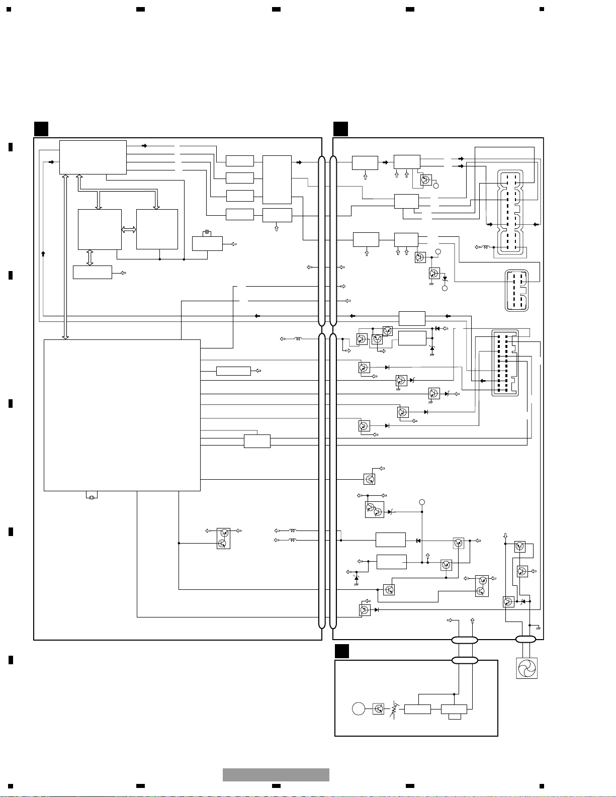
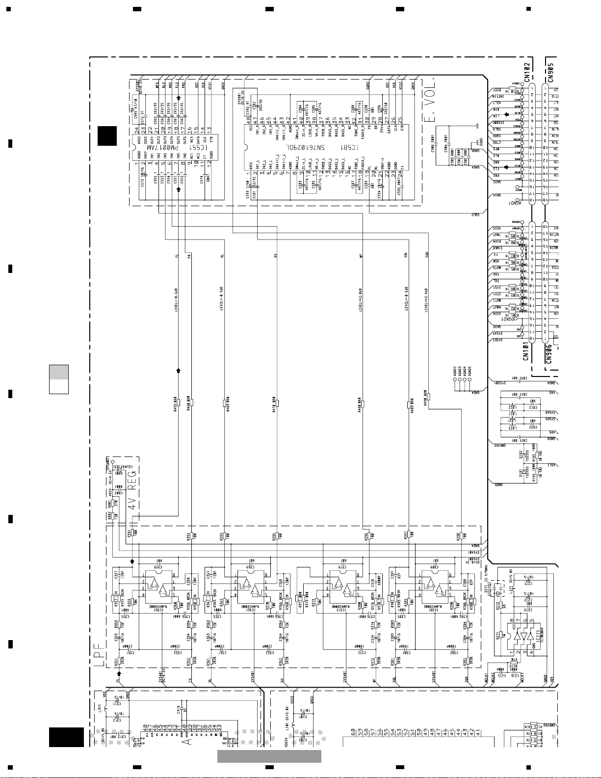
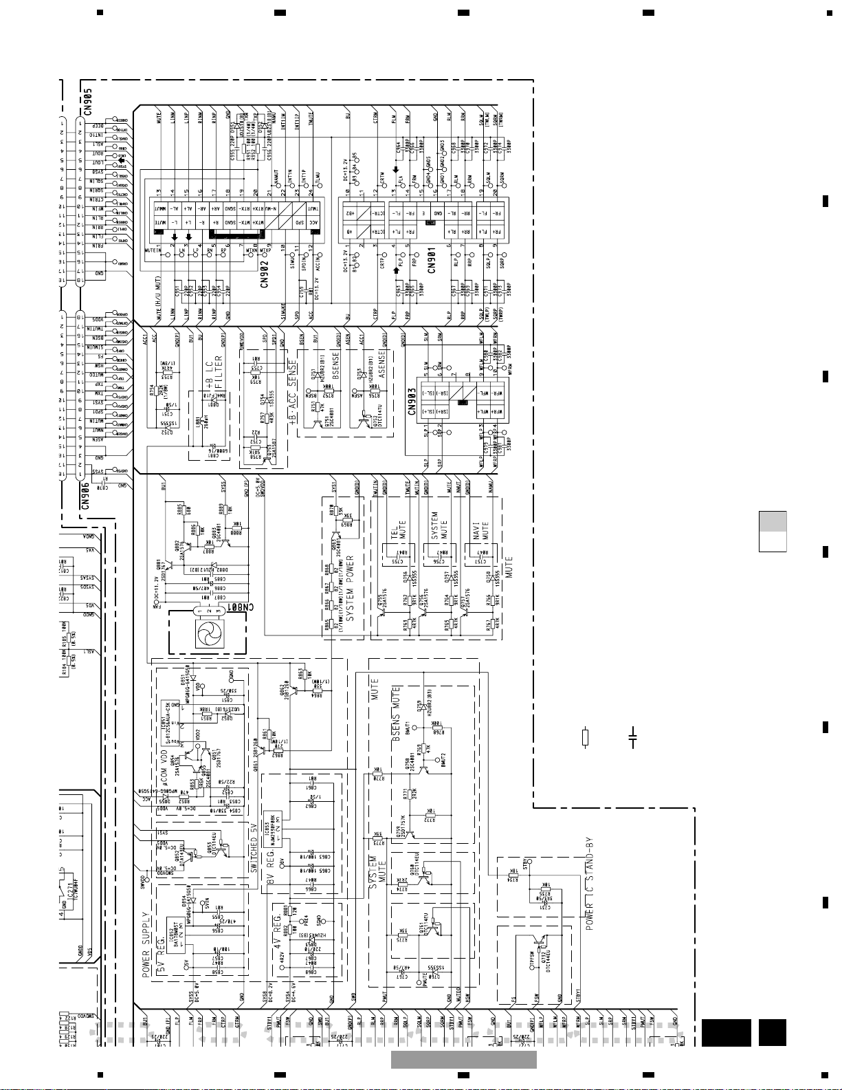
3. BLOCK DIAGRAM AND SCHEMATIC DIAGRAM
3.1 BLOCK DIAGRAM
DSP UNIT
A
27
IC251
LOUT1
LOUT2
ROUT3
LOUT4
MCLK1
39
DATA,BCK,LRCK
25
24
21
A/D & D/A
32
RIN
31
LIN
AK4529XQ
DSP
IC301
AK7706VTA
MCLK2
16
A0-16
IO0-7
we,oe
IC321
8
IC62C1024AL-70TI
DACCSN,DACCLK,DACDTI,SMUT,PDN
VDD5
IC101
PD5798A
SYSTEM CONTROLLER
IC311
AK7706VTA
MCLK3
16
(FL)
(RL)
(WF)
(SQL)
74
BEEP
ASLIN
SMUTEIN
reset
asens
bsens
TELMUTE
NAVMUTE
AVCP W
AVCI N
AVCOUT
X271
1
IC271
TC7WU04F
2
21
31
9
17
16
36
35
20
22
23
FRONT LPF
3
NJM4580MD
REAR LPF
3
NJM4580MD
WOOFER LPF
5
NJM4580MD
SQUAWKER LPF
3
NJM4580MD
7
8
RESET
1
IC186
S-80835CNUA-B8U
IC351
IC361
IC371
IC381
VDD5
(BEEP)
(ASL1)
BUS DRIVER
2
HA12187FP
1
2
IC191
1
7
5
1
4
7
2
1
8
ELECTRONIC
VOLUME
IN5
IN3
PM0017AM
IN2
SN761029DL
VDD5
IC551
IC581
48
SYS801
VDD
6
5
OUT5
OUT3
OUT2
18
20
21
19
FL
CN102
FLO
13
RLO
11
SQLO
7
WFO
10
SYS801
6
BEEP
1
3
LIN
5
RIN
4
VDD5
1
MUTI
12
ASEN
14
BSEN
3
TMUT
217
NMUT
TXH TXP
811
TXL TXM
910
B
CN905
13
11
7
10
6
1
3
5
4
CN906CN101
18
7
5
16
613
FLIN
RLIN
SQLIN
WFIN
LOUT
ROUT
VDD5
MUTIN
ASEN
BSEN
TMUTIN
NMUT
SYS8
AMP UNIT
OPE AMP
13
IC651
NJM4580MD
2
BEEP
OPE AMP
13
IC652
NJM4580MD
2
SYS4
BEEP
ASL1
Q851
Q855
VDD5
SYSTEM MUTE
Q756
SWDVDD
NAVI MUTE
Q757
SWVDD
15
STBY1
POWER AMP
14
11
POWER AMP
15
STBY1
Q854
ACC
ACC SENSE
POWER AMP
4
WOOFER
4
1
7
3
TEL MUTE
FRONT
17
IC701
19
PAL006A
1016
22
PMUT
REAR
21
IC711
23
PAL006A
9
7
(SQLP)
(SQLM)
17
IC721
19
PAL006A
10
22
Q721
PMUT
GAIN
ADJ
AUDIO INPUT
BUFFER
IC601
NJM4580MD
IC851
S-812C56AUA-C3K
µCOM VDD
Q752
Q755
SWDVDD
Q701
A
(RLP)
(RLM)
(WFLP)
(WFLM)
A
Q731
B
LINP
3
RINP
5
BU1
2
BACK UP SENSE
Q751
(FLP)
(FLM)
OUTPUT
CONNECTOR
CN901
SQL-
RL-
FL-
BU1
SQL+
RL+
FL+
CN903
ACC
SPD
MTX+
MTX-
WFL+
(SPD)
(TX+)
(TX-)
WFL-
TMUT
N-MU
MUTE
CN902
R+
L+
INPUT
CONNECTOR
(ACC)
BU1
XOUT
10 12
X101
XIN
SPEED
15
40
MUTE
SYSPW
66
MUTO
MUTEO
7
12
PMUT
Q759
SWITCHED 5V
SWDVDD
Q101
VDD5
VA5
VD5
SYSA5
17 2
SYS5SYSD5
118
Q102
SYS8
SYS4
SYS1
SYS1
9
10
Q753
SPD1SPD1
11 8
ASL UNIT
C
MIC401
MIC
PMUT
Q760
SYS4
Q758
BSENSE MUTE
5V REGULATOR
IC852
1
BA178M05T
8V REGULATOR
IC853
1
NJM2930F08K
Q863
SWDVDD
SPEED PULSE SENSE
ASL
VR401
Q401
3
3
SYSTEM POWER
5
IC401
NJM4580MD
B
SYSTEM
POWER SWITCH
Q861
STBY1
Q862
SWITCHED 5V
SYSPW1
8
SWDVDD
8
IC402
NJM4580MD
15
ASL1
34
21
SYS8
CN404
CN403
3
77
Q852
Q853
BU1
VDD5
CN801
Q881
Q882
Q883
13
SYS5
BU1
FAN MOTOR
Page 7

7
5
6
7
8
F
E
D
C
B
A
5
6
7
8
GM-8537ZT/WL
Page 8
A-aA-a A-b A-b
A-aA-a
A-b A-b
A-b A-b
A-a A-a
Large size
SCH diagram
Guide page
Detailed page
Note: When ordering service parts, be sure to refer to " EXPLODED VIEWS AND PARTS LIST" or
"ELECTRICAL PARTS LIST".
A-a
A B C
AUDIO INPUT DIFFERENTIAL
OPERATIONAL AMPLIFIER
GAIN ADJUSTMENT
SIGNAL INPUT OFF CIRCUIT
TO SUDDEN DECREASE VOLTAGE
OUTPUT OFFSET
INDICATION
OUTPUT OFFSET
INDICATION
OUTPUT OFFSET
INDICATION
AMP INPUT
C
ASL UNIT
B
AMP UNIT
CD:+8.2dBs
(1kHz 0dB)
8
1
234
12
34
F
E
D
C
B
A
GM-8537ZT/WL
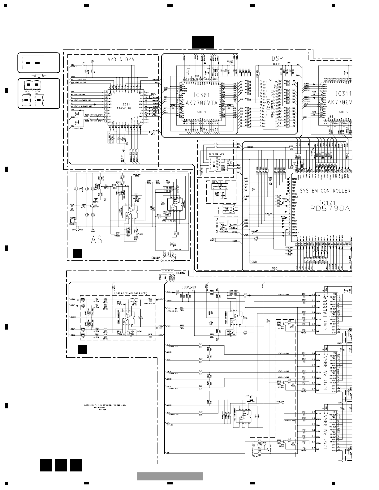
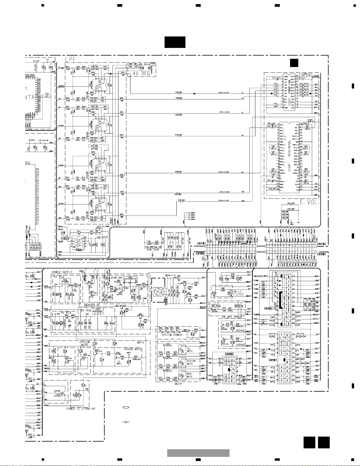
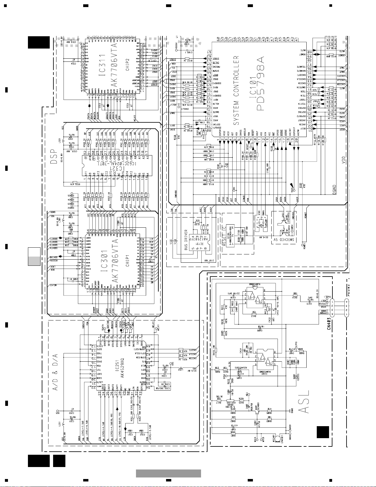
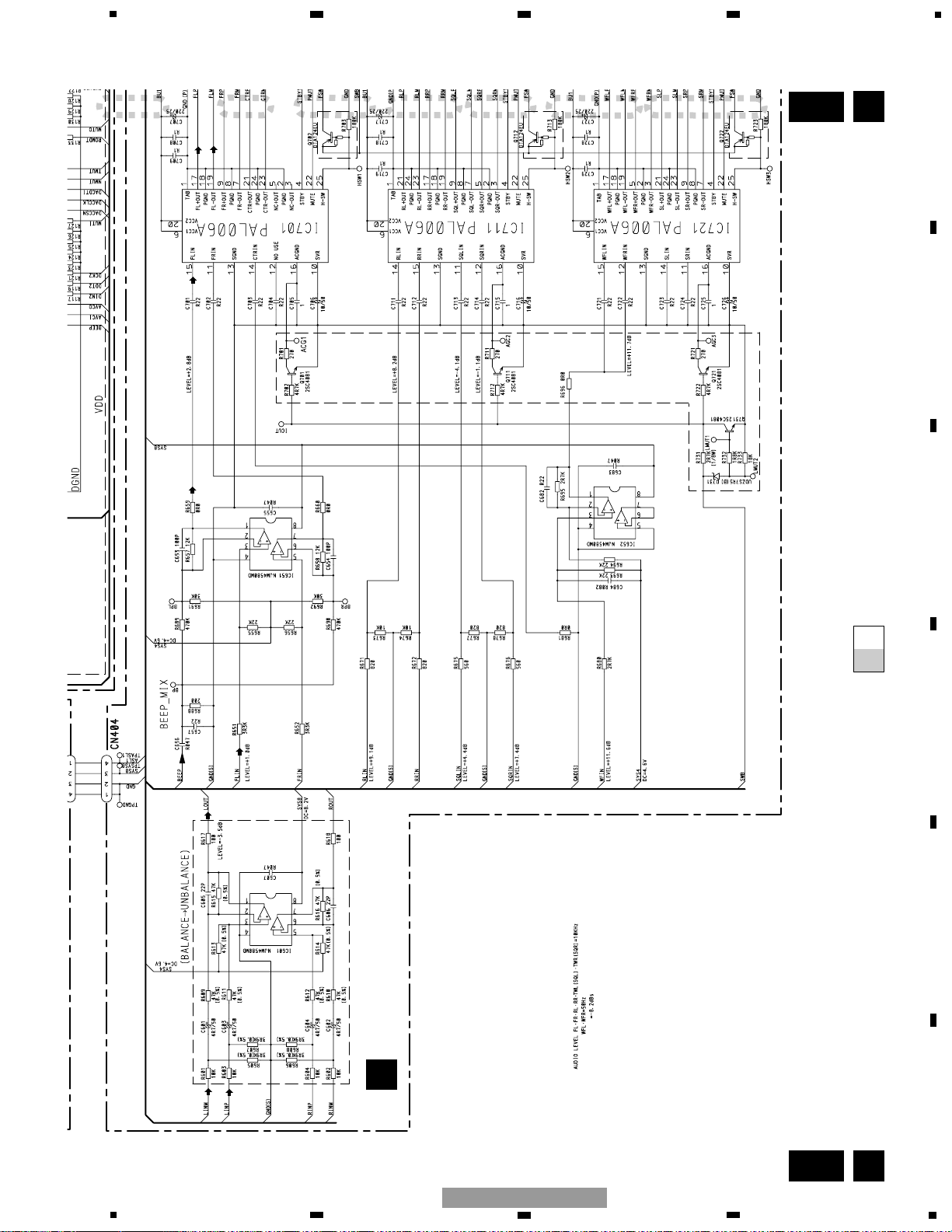
3.2 SCHEMATIC DIAGRAM (GUIDE PAGE)
Page 9
A-b
A B
OUTPUT OFFSET
INDICATION
OFFSET INDICATION
MUTE
SPEED PULSE SENSE
FAN MOTOR
CXM1266
Decimal points for resistor
and capacitor fixed values
are expressed as :
2.2 2R2
0.022 R022
←
←
Symbol indicates a resistor.
No differentiation is made between chip resistors and
discrete resistors.
NOTE :
Symbol indicates a capacitor.
No differentiation is made between chip capacitors and
discrete capacitors.
A
DSP UNIT
CD:+28.8dBs
9
5
6
7
8
F
E
D
C
B
A
5
6
7
8
GM-8537ZT/WL
Page 10
A-a
A-b
A-a
A-a
A-b
C
1
2
3
C
ASL UNIT
10
1
234
12
34
F
E
D
C
B
A
GM-8537ZT/WL
Page 11
11
5
6
7
8
F
E
D
C
B
A
5
6
7
8
GM-8537ZT/WL
A-a
A-b
A-a
A-a
A-b
B
B
4
5
6
7
8
9
10
AUDIO INPUT DIFFERENTIAL
OPERATIONAL AMPLIFIER
GAIN ADJUSTMENT
SIGNAL INPUT OFF CIRCUIT
TO SUDDEN DECREASE VOLTAGE
OUTPUT OFFSET
INDICATION
OUTPUT OFFSET
INDICATION
OUTPUT OFFSET
INDICATION
AMP INPUT
B
AMP UNIT
CD:+8.2dBs
(1kHz 0dB)
Page 12
12
1
234
12
34
F
E
D
C
B
A
GM-8537ZT/WL
A-a
A-b
A-b
1
2
3
A
DSP UNIT
Page 13
13
5
6
7
8
F
E
D
C
B
A
5
6
7
8
GM-8537ZT/WL
A-a
A-b
A-b
B
4
5
6
7
8
9
10
OUTPUT OFFSET
INDICATION
OFFSET INDICATION
MUTE
SPEED PULSE SENSE
FAN MOTOR
CXM1266
Decimal points for resistor
and capacitor fixed values
are expressed as :
2.2 2R2
0.022 R022
←
←
Symbol indicates a resistor.
No differentiation is made between chip resistors and
discrete resistors.
NOTE :
Symbol indicates a capacitor.
No differentiation is made between chip capacitors and
discrete capacitors.
CD:+28.8dBs
Page 14
14
1
234
12
34
F
E
D
C
B
A
GM-8537ZT/WL
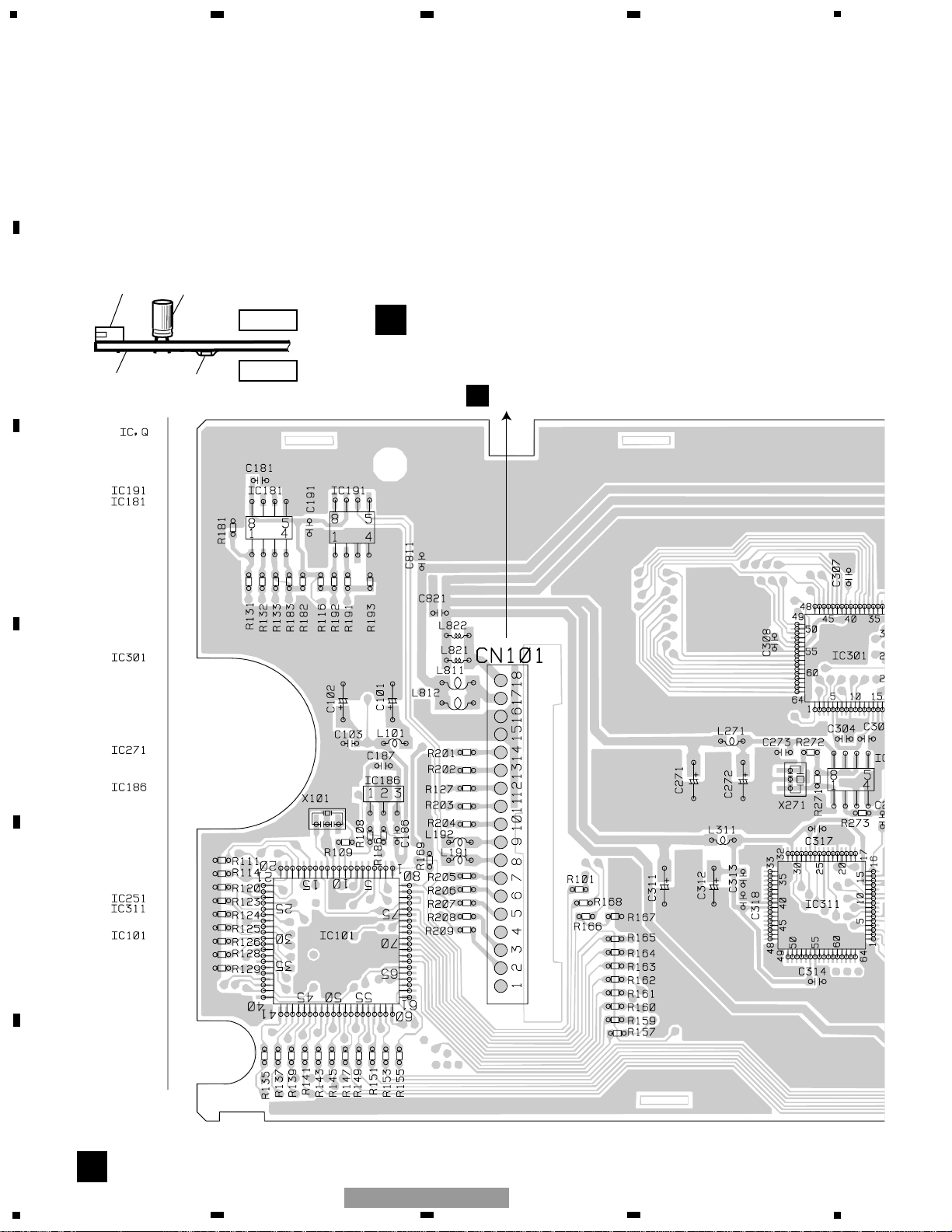
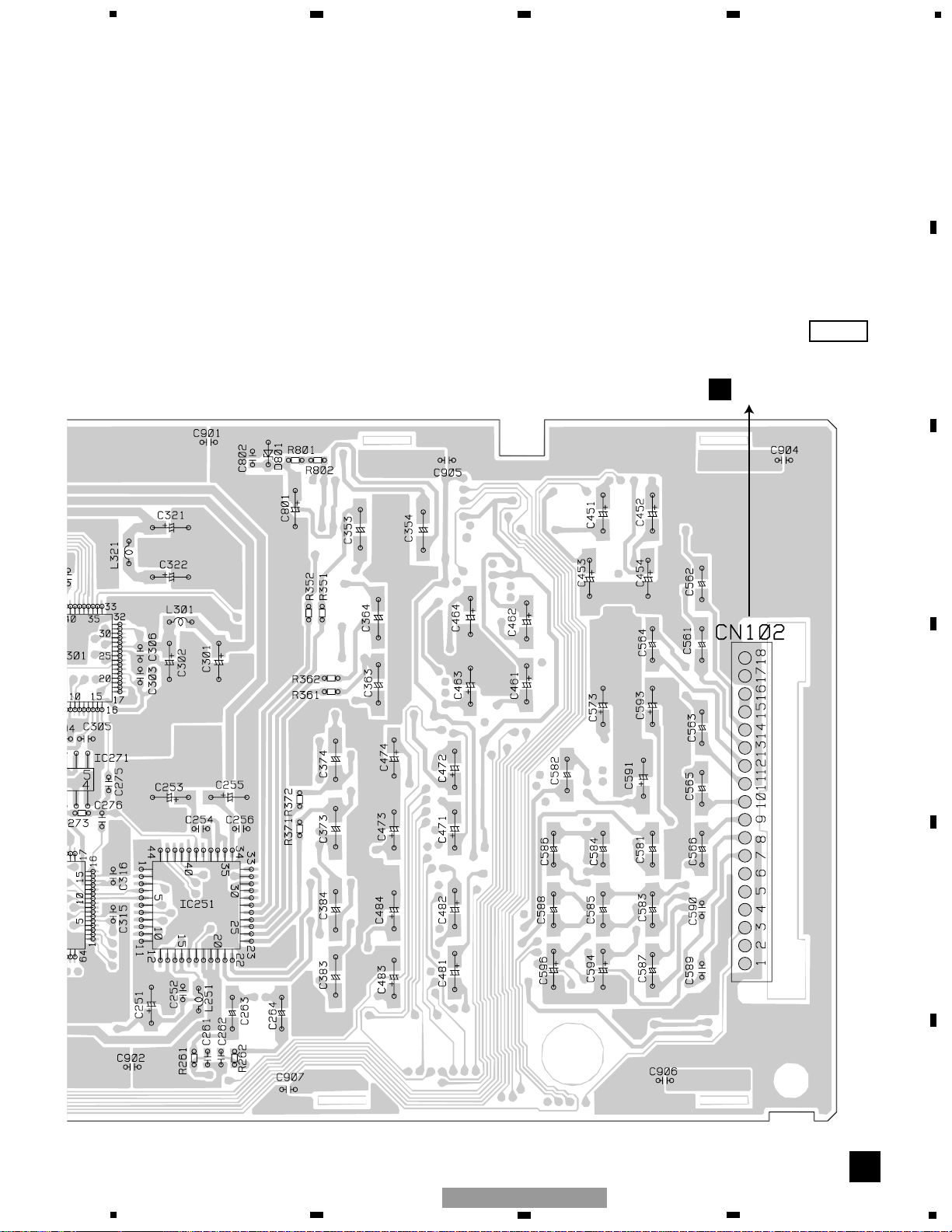
4. PCB CONNECTION DIAGRAM
4.1 DSP UNIT
Capacitor
Connector
P.C.Board
Chip Part
A
A
DSP UNIT
SIDE B
SIDE A
NOTE FOR PCB DIAGRAMS
1.The parts mounted on this PCB
include all necessary parts for
several destination.
For further information for
respective destinations, be sure
to check with the schematic dia gram.
2.Viewpoint of PCB diagrams
B
CN906
Page 15
15
5
6
7
8
F
E
D
C
B
A
5
6
7
8
GM-8537ZT/WL
A
SIDE A
B
CN905
Page 16

16
1
234
12
34
F
E
D
C
B
A
GM-8537ZT/WL
A
A
DSP UNIT
Page 17

17
5
6
7
8
F
E
D
C
B
A
5
6
7
8
GM-8537ZT/WL
A
SIDE B
Page 18

18
1
234
12
34
F
E
D
C
B
A
GM-8537ZT/WL
4.2 AMP UNIT
B
B
AMP UNIT
A
CN101
FAN MOTOR
Page 19

19
5
6
7
8
F
E
D
C
B
A
5
6
7
8
GM-8537ZT/WL
B
SIDE A
A
CN102
C
CN403
Page 20

20
1
234
12
34
F
E
D
C
B
A
GM-8537ZT/WL
B
B
AMP UNIT
Page 21

21
5
6
7
8
F
E
D
C
B
A
5
6
7
8
GM-8537ZT/WL
B
SIDE B
Page 22

22
1
234
12
34
F
E
D
C
B
A
GM-8537ZT/WL
4.3 ASL UNIT
C
C
ASL UNIT
C
ASL UNIT
SIDE A
SIDE B
B
CN404
Page 23

23
5
6
7
8
F
E
D
C
B
A
5
6
7
8
GM-8537ZT/WL
Unit Number : CWM8583
Unit Name : DSP Unit
MISCELLANEOUS
IC 101 IC PD5798A
IC 186 IC S-80835CNUA-B8U
IC 191 IC HA12187FP
IC 251 IC AK4529XQ
IC 271 IC TC7WU04F
IC 301 IC AK7706VTA
IC 311 IC AK7706VTA
IC 321 IC IC62C1024AL-70TI
IC 351 IC NJM4580MD
IC 361 IC NJM4580MD
IC 371 IC NJM4580MD
IC 381 IC NJM4580MD
IC 551 IC PM0017AM
IC 581 IC SN761029DL
Q 101 Transistor DTA144EU
Q 102 Transistor DTC144TU
D 181 Diode 1SS355
D 182 Diode 1SS355
D 801 Diode HZU4R3(B3)
L 101 Inductor LCTC1R0K2125
L 191 Inductor CTF1305
L 192 Inductor CTF1305
L 251 Inductor LCTC1R0K2125
L 252 Inductor LCTC1R0K2125
L 271 Inductor LCTC1R0K2125
L 301 Inductor LCTCR82K2125
L 311 Inductor LCTCR82K2125
L 321 Inductor LCTCR82K2125
L 811 Inductor LCTC1R0K3216
L 812 Inductor LCTC1R0K3216
L 821 Inductor LCTA2R2J2520
L 822 Inductor LCTA2R2J2520
X 101 Radiator 10.0MHz CSS1607
X 271 Radiator 22.579MHz CSS1597
RESISTORS
R 101 RS1/16S102J
R 102 RS1/16S473J
R 103 RS1/16S103J
R 104 RS1/16S102J
R 105 RS1/16S473J
R 107 RS1/16S102J
R 108 RS1/16S102J
R 109 RS1/16S681J
R 110 RS1/16S102J
R 111 RS1/16S473J
R 112 RS1/16S104J
R 113 RS1/16S104J
R 116 RS1/16S472J
R 117 RS1/16S102J
R 118 RS1/16S103J
R 119 RS1/16S102J
R 120 RS1/16S103J
R 121 RS1/16S102J
R 122 RS1/16S472J
R 123 RS1/16S473J
R 124 RS1/16S473J
R 125 RS1/16S473J
R 126 RS1/16S473J
R 127 RS1/16S102J
R 128 RS1/16S473J
R 129 RS1/16S473J
R 130 RS1/16S473J
R 133 RS1/16S0R0J
R 157 RS1/16S102J
R 158 RS1/16S473J
R 159 RS1/16S102J
R 160 RS1/16S102J
R 161 RS1/16S102J
R 162 RS1/16S102J
R 163 RS1/16S102J
R 164 RS1/16S102J
R 165 RS1/16S102J
R 166 RS1/16S102J
R 167 RS1/16S103J
R 168 RS1/16S102J
R 169 RS1/16S103J
R 170 RS1/16S473J
R 171 RS1/16S473J
R 172 RS1/16S473J
R 173 RS1/16S473J
R 182 RS1/16S473J
R 184 RS1/16S1003D
R 185 RS1/16S1003D
R 186 RS1/16S104J
R 191 RS1/16S102J
R 192 RS1/16S102J
R 193 RS1/16S473J
R 201 RS1/16S102J
R 202 RS1/16S102J
R 203 RS1/16S102J
R 204 RS1/16S102J
R 205 RS1/16S102J
R 206 RS1/16S102J
R 207 RS1/16S102J
R 208 RS1/16S102J
R 209 RS1/16S102J
R 210 RS1/16S102J
R 251 RS1/16S102J
R 252 RS1/16S102J
R 253 RS1/16S102J
R 261 RS1/16S101J
R 262 RS1/16S101J
R 271 RS1/16S105J
R 272 RS1/16S680J
R 273 RS1/16S471J
5. ELECTRICAL PARTS LIST
NOTE:
- Parts whose parts numbers are omitted are subject to being not supplied.
- The part numbers shown below indicate chip components.
Chip Resistor
RS1/_S___J,RS1/__S___J
Chip Capacitor (except for CQS.....)
CKS....., CCS....., CSZS.....
=====Circuit Symbol and No.===Part Name Part No.
--- ------ ------------------------------------------ -------------------------
=====Circuit Symbol and No.===Part Name Part No.
--- ------ ------------------------------------------ -------------------------
A
Page 24

24
1
234
12
34
F
E
D
C
B
A
GM-8537ZT/WL
R 301 RS1/16S221J
R 302 RS1/16S221J
R 303 RS1/16S221J
R 321 RS1/16S102J
R 322 RS1/16S102J
R 323 RS1/16S102J
R 324 RS1/16S102J
R 325 RS1/16S102J
R 326 RS1/16S473J
R 327 RS1/16S102J
R 328 RS1/16S102J
R 329 RS1/16S102J
R 330 RS1/16S102J
R 331 RS1/16S102J
R 332 RS1/16S102J
R 333 RS1/16S102J
R 334 RS1/16S102J
R 335 RS1/16S102J
R 336 RS1/16S102J
R 337 RS1/16S102J
R 338 RS1/16S102J
R 339 RS1/16S102J
R 340 RS1/16S102J
R 341 RS1/16S102J
R 342 RS1/16S102J
R 343 RS1/16S102J
R 344 RS1/16S102J
R 345 RS1/16S102J
R 346 RS1/16S102J
R 347 RS1/16S102J
R 348 RS1/16S102J
R 351 RS1/16S222J
R 352 RS1/16S222J
R 353 RS1/16S153J
R 354 RS1/16S153J
R 355 RS1/16S822J
R 356 RS1/16S822J
R 357 RS1/16S223J
R 358 RS1/16S223J
R 359 RS1/16S103J
R 360 RS1/16S103J
R 361 RS1/16S222J
R 362 RS1/16S222J
R 363 RS1/16S123J
R 364 RS1/16S123J
R 365 RS1/16S822J
R 366 RS1/16S822J
R 367 RS1/16S223J
R 368 RS1/16S223J
R 369 RS1/16S103J
R 370 RS1/16S103J
R 372 RS1/16S332J
R 374 RS1/16S123J
R 375 RS1/16S0R0J
R 376 RS1/16S822J
R 377 RS1/16S0R0J
R 378 RS1/16S333J
R 379 RS1/16S103J
R 380 RS1/16S103J
R 381 RS1/16S332J
R 382 RS1/16S332J
R 383 RS1/16S123J
R 384 RS1/16S123J
R 385 RS1/16S822J
R 386 RS1/16S822J
R 387 RS1/16S333J
R 388 RS1/16S333J
R 389 RS1/16S103J
R 390 RS1/16S103J
R 391 RS1/16S101J
R 392 RS1/16S101J
R 393 RS1/16S101J
R 394 RS1/16S101J
R 396 RS1/16S101J
R 397 RS1/16S101J
R 398 RS1/16S101J
R 459 RS1/16S0R0J
R 460 RS1/16S0R0J
R 469 RS1/16S0R0J
R 470 RS1/16S0R0J
R 480 RS1/16S0R0J
R 489 RS1/16S0R0J
R 490 RS1/16S0R0J
R 801 RS1/16S271J
R 802 RS1/16S121J
CAPACITORS
C 101 CEVW100M16
C 102 CEVW100M16
C 103 CKSRYB105K10
C 104 CKSRYB103K50
C 105 CKSRYB103K50
C 106 CKSRYB102K50
C 107 CKSRYB102K50
C 186 CKSRYB102K50
C 187 CKSRYB103K50
C 191 CKSRYB103K50
C 251 CEVW100M16
C 252 CKSRYB104K16
C 253 CEVW100M16
C 254 CKSRYB104K16
C 255 CEVW2R2M50
C 256 CKSRYB104K16
C 261 CCSRCH101J50
C 262 CCSRCH101J50
C 263 CEVWNP2R2M35
C 264 CEVWNP2R2M35
C 271 CEVW100M16
C 272 CEVW100M16
C 273 CKSRYB103K50
C 275 CKSRYB102K50
C 276 CKSRYB102K50
C 301 CEVW100M16
C 302 CEVW100M16
C 303 CKSRYB103K50
C 304 CKSRYB104K16
C 305 CKSRYB104K16
C 306 CKSRYB104K16
C 307 CKSRYB104K16
C 308 CKSRYB104K16
C 311 CEVW100M16
C 312 CEVW100M16
C 313 CKSRYB103K50
C 314 CKSRYB104K16
C 315 CKSRYB104K16
C 316 CKSRYB104K16
C 317 CKSRYB104K16
C 318 CKSRYB104K16
C 321 CEVW100M16
C 322 CEVW100M16
C 323 CKSRYB103K50
C 351 CKSRYB222K50
=====Circuit Symbol and No.===Part Name Part No.
--- ------ ------------------------------------------ -------------------------
=====Circuit Symbol and No.===Part Name Part No.
--- ------ ------------------------------------------ -------------------------
Page 25

25
5
6
7
8
F
E
D
C
B
A
5
6
7
8
GM-8537ZT/WL
C 352 CKSRYB222K50
C 353 CEVWNP100M16
C 354 CEVWNP100M16
C 355 CKSRYB102K50
C 356 CKSRYB102K50
C 357 CCSRCH121J50
C 358 CCSRCH121J50
C 359 CKSRYB103K50
C 361 CKSRYB222K50
C 362 CKSRYB222K50
C 363 CEVWNP100M16
C 364 CEVWNP100M16
C 365 CKSRYB102K50
C 366 CKSRYB102K50
C 367 CCSRCH121J50
C 368 CCSRCH121J50
C 369 CKSRYB103K50
C 372 CKSRYB182K50
C 374 CEVWNP100M16
C 376 CKSRYB102K50
C 378 CKSRYB682K50
C 379 CKSRYB103K50
C 381 CKSRYB182K50
C 382 CKSRYB182K50
C 383 CEVWNP100M16
C 384 CEVWNP100M16
C 385 CKSRYB102K50
C 386 CKSRYB102K50
C 387 CCSRCH820J50
C 388 CCSRCH820J50
C 389 CKSRYB103K50
C 551 CKSYB105K16
C 552 CKSYB105K16
C 553 CKSYB105K16
C 554 CKSYB105K16
C 555 CKSYB105K16
C 561 CEVWNP2R2M35
C 562 CEVWNP2R2M35
C 563 CEVWNP2R2M35
C 564 CEVWNP2R2M35
C 565 CEVWNP2R2M35
C 572 CKSRYB104K16
C 573 CEVW100M16
C 574 CKSRYB473K50
C 581 CEVWNP2R2M35
C 582 CEVWNP2R2M35
C 583 CEVWNP4R7M16
C 584 CEVWNP4R7M16
C 585 CEVWNP4R7M16
C 586 CEVWNP4R7M16
C 587 CEVWNP4R7M16
C 588 CEVWNP4R7M16
C 589 CKSRYB103K50
C 590 CKSRYB103K50
C 591 CEVW470M10
C 592 CKSRYB104K16
C 593 CEVW1R0M50
C 594 CEVW100M16
C 595 CKSRYB473K50
C 596 CEVW2R2M50
C 801 CEVW101M16
C 802 CKSRYB102K50
C 811 CKSRYB103K50
C 812 CKSRYB103K50
C 821 CKSRYB103K50
C 822 CKSRYB103K50
C 831 CKSRYB103K50
C 901 CKSRYB102K50
C 902 CKSRYB102K50
C 903 CKSRYB102K50
C 904 CKSRYB102K50
C 906 CKSRYB102K50
Unit Number : CWM8305
Unit Name : ASL Unit
MISCELLANEOUS
IC 401 IC NJM4580MD
IC 402 IC NJM4580MD
Q 401 Transistor 2SC4081
D 401 Diode HZU4R3(B3)
D 402 Diode 1SS355
VR 401 Semi-fixed 3.3kΩ(OB) CCP1393
MIC 401 Microphone CPM1011
RESISTORS
R 401 RS1/16S222J
R 402 RS1/16S683J
R 403 RS1/16S103J
R 404 RS1/16S472J
R 405 RS1/16S471J
R 406 RS1/16S271J
R 407 RS1/16S684J
R 408 RS1/16S682J
R 409 RS1/16S472J
R 410 RS1/16S472J
R 411 RS1/16S473J
R 412 RS1/16S153J
R 413 RS1/16S153J
R 414 RS1/16S101J
R 417 RS1/16S1800D
R 418 RS1/16S562J
R 419 RS1/16S1002D
R 420 RS1/16S2002D
R 422 RS1/16S121J
R 425 RS1/16S472J
CAPACITORS
C 401 CEJQ470M10
C 402 CEJQ470M10
C 403 CEALR68M50
C 404 CEJQ100M50
C 405 CEJQ470M10
C 406 CCSRCH101J50
C 407 CEJQ470M10
C 408 CEJQ100M50
C 409 CKSRYB473K25
C 410 CEJQNP220M10
C 411 CKSRYB104K16
C 412 CEJQNP100M16
C 413 CEJQNP100M16
C 414 CKSRYB103K50
C 415 CKSRYB223K50
C 416 CKSRYB474K10
=====Circuit Symbol and No.===Part Name Part No.
--- ------ ------------------------------------------ -------------------------
=====Circuit Symbol and No.===Part Name Part No.
--- ------ ------------------------------------------ -------------------------
C
Page 26

26
1
234
12
34
F
E
D
C
B
A
GM-8537ZT/WL
Unit Number : CWM8584
Unit Name : Amp Unit
MISCELLANEOUS
IC 601 IC NJM4580MD
IC 651 IC NJM4580MD
IC 652 IC NJM4580MD
IC 701 IC PAL006A
IC 711 IC PAL006A
IC 721 IC PAL006A
IC 851 IC S-812C56AUA-C3K
IC 852 IC BA178M05T
IC 853 IC NJM2930F08K
Q 701 Transistor 2SC4081
Q 702 Transistor DTA124EU
Q 711 Transistor 2SC4081
Q 712 Transistor DTA124EU
Q 721 Transistor 2SC4081
Q 722 Transistor DTA124EU
Q 731 Transistor 2SC4081
Q 732 Transistor DTC144EU
Q 751 Transistor 2SC4081
Q 752 Transistor DTC114TU
Q 753 Transistor 2SA1587
Q 755 Transistor 2SA1576
Q 756 Transistor 2SA1576
Q 757 Transistor 2SA1576
Q 758 Transistor 2SC4081
Q 759 Transistor 2SD1757K
Q 760 Transistor DTC114EU
Q 761 Transistor DTC114EU
Q 851 Transistor 2SD1767
Q 852 Transistor DTA143EU
Q 853 Transistor DTC114EU
Q 854 Transistor 2SA1576
Q 855 Transistor 2SC4081
Q 861 Transistor 2SB1260
Q 862 Transistor 2SB1260
Q 863 Transistor 2SC4081
Q 881 Transistor 2SD1767
Q 882 Transistor 2SA1576
Q 883 Transistor 2SC4081
D 731 Diode UDZS7R5(B)
D 751 Diode HZU8R2(B1)
D 752 Diode 1SS355
D 753 Diode HZU8R2(B1)
D 754 Diode 1SS355
D 756 Diode 1SS355
D 757 Diode 1SS355
D 758 Diode 1SS355
D 759 Diode HZU8R2(B3)
D 760 Diode 1SS355
D 851 Diode MPG06G-6415G50
D 852 Diode UDZS16(B)
D 853 Diode HZU4R3(B3)
D 854 Diode MPG06G-6415G50
D 855 Diode MPG06G-6415G50
D 881 Diode RM4LFJ10
D 882 Diode HZU12(B2)
D 951 Diode UDZS18(B)
D 952 Diode UDZS18(B)
L 881 Choke Coil 260µH CTH1240
RESISTORS
R 601 RS1/16S1002D
R 602 RS1/16S1002D
R 603 RS1/16S1002D
R 604 RS1/16S1002D
R 605 RS1/16S3901D
R 606 RS1/16S3901D
R 607 RS1/16S3901D
R 608 RS1/16S3901D
R 609 RS1/16S4702D
R 610 RS1/16S4702D
R 611 RS1/16S4702D
R 612 RS1/16S4702D
R 613 RS1/16S4702D
R 614 RS1/16S4702D
R 615 RS1/16S4702D
R 616 RS1/16S4702D
R 617 RS1/16S101J
R 618 RS1/16S101J
R 651 RS1/16S332J
R 652 RS1/16S332J
R 655 RS1/16S223J
R 656 RS1/16S223J
R 657 RS1/16S123J
R 658 RS1/16S123J
R 659 RS1/16S0R0J
R 660 RS1/16S0R0J
R 671 RS1/16S821J
R 672 RS1/16S821J
R 673 RS1/16S103J
R 674 RS1/16S103J
R 675 RS1/16S561J
R 676 RS1/16S561J
R 677 RS1/16S821J
R 678 RS1/16S821J
R 680 RS1/16S272J
R 681 RS1/16S0R0J
R 688 RS1/16S201J
R 689 RS1/16S474J
R 690 RS1/16S474J
R 691 RS1/16S303J
R 692 RS1/16S303J
R 693 RS1/16S223J
R 694 RS1/16S223J
R 695 RS1/16S272J
R 696 RS1/16S0R0J
R 701 RS1/16S271J
R 702 RS1/16S472J
R 703 RS1/16S184J
R 711 RS1/16S271J
R 712 RS1/16S472J
R 713 RS1/16S184J
R 721 RS1/16S271J
R 722 RS1/16S472J
R 723 RS1/16S184J
R 731 RS1/8S272J
R 732 RS1/16S182J
R 733 RS1/16S183J
R 734 RS1/16S183J
R 735 RS1/16S103J
R 751 RS1/16S473J
R 752 RS1/16S104J
R 753 RS1/8S472J
R 754 RS1/8S222J
R 756 RS1/16S104J
R 757 RS1/16S432J
R 758 RS1/16S512J
R 759 RS1/16S103J
R 762 RS1/16S912J
R 763 RS1/16S472J
R 764 RS1/16S912J
=====Circuit Symbol and No.===Part Name Part No.
--- ------ ------------------------------------------ -------------------------
=====Circuit Symbol and No.===Part Name Part No.
--- ------ ------------------------------------------ -------------------------
B
Page 27

27
5
6
7
8
F
E
D
C
B
A
5
6
7
8
GM-8537ZT/WL
=====Circuit Symbol and No.===Part Name Part No.
--- ------ ------------------------------------------ -------------------------
R 765 RS1/16S472J
R 766 RS1/16S912J
R 767 RS1/16S472J
R 768 RS1/16S104J
R 769 RS1/16S473J
R 770 RS1/16S103J
R 771 RS1/16S222J
R 772 RS1/16S103J
R 773 RS1/16S333J
R 774 RS1/16S272J
R 775 RS1/16S333J
R 851 RS1/16S182J
R 852 RS1/10S471J
R 853 RS1/16S562J
R 861 RS1/16S103J
R 862 RS1/10S271J
R 863 RS1/16S103J
R 864 RS1/10S331J
R 865 RS1/10S820J
R 866 RS1/10S820J
R 867 RS1/10S820J
R 868 RS1/10S820J
R 869 RS1/16S333J
R 870 RS1/16S333J
R 881 RS1/16S121J
R 882 RS1/16S101J
R 885 RS1/16S681J
R 886 RS1/16S103J
R 887 RS1/16S103J
R 888 RS1/16S103J
R 889 RS1/16S103J
R 951 RS1/4S101J
R 952 RS1/4S101J
CAPACITORS
C 601 CEAT4R7M50
C 602 CEAT4R7M50
C 603 CEAT4R7M50
C 604 CEAT4R7M50
C 605 CCSRCH220J50
C 606 CCSRCH220J50
C 607 CKSRYB473K50
C 653 CCSRCH101J50
C 654 CCSRCH101J50
C 655 CKSRYB473K50
C 656 CKSRYB473K50
C 657 CKSRYB224K10
C 682 CKSRYB224K16
C 683 CKSRYB473K50
C 684 CKSRYB823K16
C 701 CFTNA224J50
C 702 CFTNA224J50
C 703 CFTNA224J50
C 704 CFTNA224J50
C 705 CFTNA105J50
C 706 CEHAT100M50
C 707 CEHAT221M25
C 708 CKSQYB104K25
C 709 CKSQYB104K25
C 711 CFTNA224J50
C 712 CFTNA224J50
C 713 CFTNA224J50
C 714 CFTNA224J50
C 715 CFTNA105J50
C 716 CEAT100M50
C 717 CEHAT221M25
C 718 CKSQYB104K25
C 719 CKSQYB104K25
C 721 CFTNA224J50
C 722 CFTNA224J50
C 723 CFTNA224J50
C 724 CFTNA224J50
C 725 CFTNA105J50
C 726 CEAT100M50
C 727 CEHAT221M25
C 728 CKSQYB104K25
C 729 CKSQYB104K25
C 731 CEAT3R3M50
C 751 CEAT1R0M50
C 752 CKSQYB224K25
C 753 CKSQYB103K50
C 755 CKSQYB473K50
C 756 CKSQYB473K50
C 757 CKSQYB473K50
C 759 CKSQYB103K50
C 767 CEAT4R7M50
C 851 CEAT331M25
C 852 CEHATR22M50
C 853 CKSRYB103K50
C 854 CEAT331M10
C 855 CKSRYB103K50
C 856 CEHAT471M25
C 857 100µF/10V CCH1282
C 858 CKSRYB473K50
C 861 CKSRYB103K50
C 862 CEHAT1R0M50
C 863 100µF/10V CCH1282
C 865 100µF/10V CCH1282
C 866 CKSRYB473K50
C 867 CEAT221M10
C 868 CKSRYB473K50
C 870 CKSRYB104K16
C 881 6800µF/16V CCH1390
C 885 CKSQYB103K50
C 886 CEHAT4R7M50
C 887 CKSQYB103K50
C 951 CCSQCH221J50
C 952 CCSQCH221J50
C 953 CCSQCH221J50
C 954 CCSQCH221J50
C 955 CCSQCH221J50
C 956 CCSQCH221J50
C 963 CKSQYB332K50
C 964 CKSQYB332K50
C 965 CKSQYB332K50
C 966 CKSQYB332K50
C 967 CKSQYB332K50
C 968 CKSQYB332K50
C 969 CKSQYB332K50
C 970 CKSQYB332K50
C 971 CKSQYB332K50
C 972 CKSQYB332K50
C 973 CKSQYB332K50
C 974 CKSQYB332K50
C 979 CKSQYB332K50
C 980 CKSQYB332K50
C 981 CKSQYB332K50
C 982 CKSQYB332K50
Miscellaneous Parts List
Fan Motor CXM1266
=====Circuit Symbol and No.===Part Name Part No.
--- ------ ------------------------------------------ -------------------------
Page 28

28
1
234
12
34
F
E
D
C
B
A
GM-8537ZT/WL
6. ADJUSTMENT
- Jigs
When attaching the DSP unit to the AMP unit, use "Jigs" (GGD1245).
GGD1245
Page 29

29
5
6
7
8
F
E
D
C
B
A
5
6
7
8
GM-8537ZT/WL
FX-MG9187ZT/EW(Pioneer AMP Model)
FX-MG9687ZT/EW(Marklevinson AMP Model)
FX-MG9087ZT/EW(Pioneer AMP Model)
FX-MG9587ZT/EW(Marklevinson AMP Model)
CD-R8137ZT/E
EMV
20P12P
26P 28P
10P 24P
AMP
20P
NAVI
18P 8P 6P 10P
25P
AM/FM TUNER
8P
REAR CON.
GM-8537ZT/WL
Marklevinson AMP
GEX-T8037ZT/EW
HEAD UNIT
FR+
FR-
10P 20P 24P
GGD1344
GGD1345
GGD1339
AUI+
AUI-
20P
12P
8P 25P 8P6P
18P 8P 6P
Bullet
connector
(ACC,+B,
ILL,GND)
AUO+
AUO-
26P 28P
6P12P
10P
12P 5P
Non-connected
For Head unit
For Rear
con.
For TV For TV For EMV
Bullet connector
(+B,GND,SP Line)
Bullet connector
(WFSP Line)
Bullet connector
(ACC,+B,ILL,GND)
To front right SP
Non-connected
Non-connected Non-connectedNon-connected
For XMTUNER
- Connection Diagram
Page 30

30
1
234
12
34
F
E
D
C
B
A
GM-8537ZT/WL
- Connection Diagram
FX-MG9187ZT/Q1(Pioneer AMP Model)
FX-MG9687ZT/Q1(Marklevinson AMP Model)
CD-R8137ZT/E
EMV
20P12P
26P 28P
10P 24P
AMP
20P
NAVI
18P 8P 6P 10P
25P
AM/FM TUNER
8P
REAR CON.
GM-8537ZT/WL
Marklevinson AMP
GEX-T8137ZT/Q1
HEAD UNIT
FR+
FR-
10P 20P 24P
GGD1344
GGD1345
GGD1339
AUI+
AUI-
20P
12P
8P 25P 8P6P
18P 8P 6P
Bullet
connector
(ACC,+B,
ILL,GND)
AUO+
AUO-
26P 28P
6P12P
10P
12P 5P
Non-connected
For Head unit
For Rear
con.
For TV For TV For EMV
Bullet connector
(+B,GND,SP Line)
Bullet connector
(WFSP Line)
Bullet connector
(ACC,+B,ILL,GND)
To front right SP
Non-connected
Non-connected Non-connectedNon-connected
For XM TUNER
Page 31

31
5
6
7
8
F
E
D
C
B
A
5
6
7
8
GM-8537ZT/WL
- Connection Diagram
FX-MG9187ZT/UC(Pioneer AMP Model)
FX-MG9687ZT/UC(Marklevinson AMP Model)
CD-R8137ZT/E
HEAD UNIT
NAVI ECU
20P12P
26P 28P
12P
10P 24P
AMP
XM TUNER
20P
EMV
18P 8P 6P 10P
25P
AM/FM TUNER
8P
REAR CON.
GM-8537ZT/WL
Marklevinson AMP
GEX-T8137ZT/UC
GEX-*****XM/UC
FR+
FR-
10P 20P 24P
GGD1344
GGD1345
GGD1339
AUI+
AUI-
20P
12P
8P 25P 8P6P
18P 8P 6P
Bullet
connector
(ACC,+B,
ILL,GND)
AUO+
AUO-
26P 28P
6P
12P
10P
12P 5P
Non-connected
For Head unit
For Rear
con.
For TV For TV For EMV
Bullet connector
(+B,GND,SP Line)
Bullet connector
(WFSP Line)
Bullet connector
(ACC,+B,ILL,GND)
To front right SP
Non-connected
Non-connected Non-connected
Page 32

32
1
234
12
34
F
E
D
C
B
A
GM-8537ZT/WL
- Connection Diagram
FX-MG8087ZT/ES(Pioneer AMP Model)
FX-MG8187ZT/ES(Pioneer AMP Model)
FX-MG8587ZT/ES(Marklevinson AMP Model)
FX-MG8687ZT/ES(Marklevinson AMP Model)
CD-R8137ZT/E
20P12P
10P 24P
AMP
20P
25P
AM/FM TUNER
8P
REAR CON.
GEX-T9006ZT/ES
HEAD UNIT
FR+
FR-
GGD1344
GGD1345
24P
GGD1340
20P
24P10P 20P
GGD1341
12P
For XM TUNER
Bullet connector
(ACC,+B,ILL,GND)
Bullet connector
(+B,GND,SP Line)
Bullet connector
(WFSP Line)
Non-connected
24P
20P
12P
25P 8P
20P
GM-8537ZT/WL
Marklevinson AMP
Page 33

33
5
6
7
8
F
E
D
C
B
A
5
6
7
8
GM-8537ZT/WL
- Connection Diagram
FX-MG8087ZT/EW(Pioneer AMP Model)
FX-MG8187ZT/EW(Pioneer AMP Model)
CD-R8137ZT/E
20P12P
10P 24P
AMP
20P
25P
AM/FM TUNER
8P
REAR CON.
GM-8537ZT/WL
GEX-T9006ZT-02/EW
HEAD UNIT
20P
12P
FR+
FR-
GGD1344
GGD1345
25P 8P
24P
GGD1340
24P
20P
24P10P 20P
GGD1341
12P
For XMTUNER
Bullet connector
(ACC,+B,ILL,GND)
Bullet connector
(+B,GND,SP Line)
Bullet connector
(WFSP Line)
Non-connected
20P
Page 34

34
1
234
12
34
F
E
D
C
B
A
GM-8537ZT/WL
- Connection Diagram
FX-MG8187ZT/UC(Pioneer AMP Model)
FX-MG8687ZT/UC(Marklevinson AMP Model)
20P12P
12P
10P 24P
24P10P
AMP
XM TUNER
20P
20P
25P
AM/FM TUNER
8P
REAR CON.
GM-8537ZT/WL
Marklevinson AMP
CD-R8137ZT/E
GEX-T8137ZT/UC
GEX-M8087XMZT/XN/UC
FR+
FR-
GGD1344
GGD1345
24P
GGD1340
24P
20P
20P
GGD1341
12P
20P12P 25P 8P
HEAD UNIT
Bullet connector
(ACC,+B,ILL,GND)
Bullet connector
(+B,GND,SP Line)
Bullet connector
(WFSP Line)
Page 35

35
5
6
7
8
F
E
D
C
B
A
5
6
7
8
GM-8537ZT/WL
7. GENERAL INFORMATION
7.1 DIAGNOSIS
7.1.1 DISASSEMBLY
1
1
3
- Removing the 86285-50110 (Fig.1)
- Removing the Case (Fig.1)
- Removing the Bracket (Fig.2)
Remove the two screws and then remove
the 86285-50110.
Remove the four screws and then remove
the Case.
Remove the three screws and then
remove the Bracket.
Fig.1
Fig.2
DSP Unit
2
- Removing the 86286-50040 (Fig.1)
Remove the three screws and then remove
the 86286-50040.
Case
3
3
3
3
2
2
2
1
1
86285-50110 86286-50040
1
1
1
Bracket
2
- Removing the DSP Unit (Fig.2)
Straighten the tabs at seven
locations indicated.
2
2
2
2
2
2
2
3
3 3
3
3
Remove the four screws and then
remove the DSP Unit and the
Shield together.
Page 36

36
1
234
12
34
F
E
D
C
B
A
GM-8537ZT/WL
< Cautions and Techniques for removing the DSP Unit >
In addition to the explanation on the previous page, there are some cautions and techniques for removing
the DSP Unit.
1 Use a pair of tweezers as a lever.
Insert the tips into the upper side-slits (A in Rear View) and get the bottom side of the Shield.
Push the tweezers down in the direction indicated by an arrow in Side View.
- Rear View
A
- Side View
Tweezers
DSP UNIT
A
Shield
AMP UNIT
2 Now one of the 18-pin connectors gets disconnected from the DSP Unit by doing 1 so that it becomes
easier to detach the DSP Unit.
Lift and remove the DSP Unit and the Shield together.
Be careful not to give any stress to the 18-pin connectors on both sides when removing the DSP Unit
and the Shield.
Page 37

37
5
6
7
8
F
E
D
C
B
A
5
6
7
8
GM-8537ZT/WL
1
3
3
2
3
- Removing the Amp Uint (Fig.3)
Remove the eight screws and then
remove the Heat Sink.
Straighten the tab at location indicated.
Remove the four screws and then
remove the Amp Unit.
Fig.3
Amp Unit
Heat Sink
1
1
1
1
1
1
1
1
2
3
3
- " Pawl bending and soldering " points of the pawls for securing the base plate of a shielded case (bottom case).
The portion marked by is a point in which pawl bending and soldering are necessary.
DSP UNIT
Page 38

38
1
234
12
34
F
E
D
C
B
A
GM-8537ZT/WL
7.1.2 CONNECTOR FUNCTION DESCRIPTION
A
WFR+
WFL+
(SR+)
B
(SL+)
C
A
SPDACC
WFL-
MTX+
WFR-
(SR-)
MTX-
(SL-)
SGND
R+
MUTE
L+R-
L-
B
TMUT
N-MU
RTX+
RTX-
SGND
AR+
AR-
AL+
AL-
MMUT
FR+
FL+
RR+
RL+
FR+
FL+
(CTR+)
+B
C
GND
FR-
FL-
RR-
RL-
E
FR-
FL-
(CTR-)
+B2
Page 39

39
5
6
7
8
F
E
D
C
B
A
5
6
7
8
GM-8537ZT/WL
7.1.3 THE METHOD OF DISTINGUISHING DEFECTIVE DSP IC (IC301 OR IC311)
DURING DSP ERROR
If anything is wrong with IC301 or IC311 (AK7706VTA), DSP error will result. Under the
occurrence of the error, DSP IC will be required to execute the initialization command by the
system microcomputer until DSP IC gets back to normal. However, the error cannot be fixed
because of defective IC, and so the initialization will be commanded over and over again.
While this condition prevails, follow the description below about observations of the IC101
waveforms to distinguish defective DSP IC.
[Observations of the IC101 waveforms]
• First, perform the 67 pin (drst) waveform observations.
When DSP error occurs, this waveform repeats "Hi/Low" shapes after ACC ON.
For reference sake, when there is no problem, the 67 pin (drst) waveform should
keep "Hi" continuously after ACC ON.
• Then, perform the 19 pin (DSPCHIP) waveform observations.
While the 67 pin (drst) waveform stays at "Low", perform the 19 pin waveform
observations and produce a decision.
• The 19 pin (DSPCHIP) waveform during DSP error
Keeping "Hi" continuously : IC301 is defective.
Proper IC311 operation is not guaranteed, though.
After making repairs on IC301, re-perform the 67
pin (drst) waveform observations. Keeping "Hi"
continuously on the 67 pin (drst) waveform shows
that DSP IC functions normally.
Keeping "Low" continuously : IC311 is defective. IC301 is OK. After making repairs
on IC311, re-perform the 67 pin (drst) waveform
observations. Keeping "Hi" continuously on the 67 pin
(drst) waveform shows that DSP IC functions normally.
[Observations of the IC101 waveform (for drst and DSPCHIP)]
500ms
Hi(5V)
- The 67 pin (drst) waveform
during DSP error
Low(0V)
The 19 pin (DSPCHIP) waveform
1 The waveform to indicate that
IC301 is defective
(No information about IC311)
2 The waveform to indicate that
IC311 is defective
Hi(5V)
Low(0V)
Hi(5V)
Low(0V)
- The 67 pin (drst) waveform
during normal DSP operation
Hi(5V)
Low(0V)
Page 40

40
1
234
12
34
F
E
D
C
B
A
GM-8537ZT/WL
DSP UNIT
SIDE A
CN101
CN102
19pin
DSPCHIP
IC101
67pin
drst
Page 41

41
5
6
7
8
F
E
D
C
B
A
5
6
7
8
GM-8537ZT/WL
7.2 IC
- Pin Functions (PD5798A)
Pin No. Pin Name I/O Function and Operation
1 DSPCK1 O DSP 1 I/F serial clock output
2 VCS2 O Electronic volume 2 strobe output
3 VCS1 O Electronic volume 1 strobe output
4 VDT O Electronic volume serial data output
5 VCK O Electronic volume serial clock output
6 CNVSS I Connect to GND
7 MODEL0 Not used
8 PDN O Codec power down output
9 reset I Reset input
10 XOUT O System clock output
11 VSS GND
12 XIN I System clock input (10MHz)
13 VCC Power supply (+5V)
14 nmi I Connect to VCC
15 SPEED I Speed sensor pulse input
16 bsens I Backup sense input
17 asens I ACC sense input
18 AVCINT I AVC-LAN data input
19 DSPCHIP O DSP error output
20 AVCPW O AVC-LAN driver power output
21 BEEP O Beep pulse output
22 AVCIN I AVC-LAN data input
23 AVCOUT O AVC-LAN data output
24 DSPOUT2 O DSP 2 I/F serial data output
25 DSPIN2 I DSP 2 I/F serial data input
26 DSPCK2 O DSP 2 I/F serial clock output
27 TESTIN I Test program input
28 TSOUT O Test serial data output
29 TSIN I Test serial data input
30 TSCK I Test serial clock input
31 SMUTEIN I System mute input
32 DACCSN O Codec control chip select output
33 DACCCLK O Codec control clock output
34 DACCDTI O Codec control data output
35 NAVMUTE I NAVI mute input
36 TELMUTE I TEL mute input
37,38 NC Not used
39 ROMDT I/O ROM correction data input / output
40 MUTE O System mute output
41-62 NC Not used
63 dirst O DSP reset output
64 calib O Power IC control output
65 PWSENS I Power IC control input
66 SYSPW O System power output
67 drst O DSP reset output (DSP)
68 drq2 O DSP 2 request output
69 DSDRDY2 I DSP 2 data ready input
70 RDY2 I DSP 2 write in ready input
71 DRQ1 O DSP 1 request output
72 DSDRDY1 I DSP 1 data ready input
73 RDY1 I DSP 1 write in ready input
74 ASLIN I ASL noise input
75 AVSS GND for microcomputer AD
76 SMUTE O Codec soft mute output
77 VREF I Reference input for microcomputer AD
78 AVCC Power supply for microcomputer AD
79 DSPIN1 I DSP 1 I/F serial data input
80 DSPOUT1 O DSP 1 I/F serial data output
Page 42

42
1
234
12
34
F
E
D
C
B
A
GM-8537ZT/WL
VREF
123
VDD
VSS
OUT
S-80835CNUA-B8U
123
VIN
VOUT
GND
Reference
Voltage
S-812C56AUA-C3K
132
A OUTPUT
A -INPUT
A +INPUT
V-
B +INPUT
B -INPUT
B OUTPUT
V+
4
5678
+
+
A
B
NJM4580MD
IC62C1024AL-70TI
* PD5798A
IC's marked by * are MOS type.
Be careful in handling them because they are very
80
1
20
21
61
40
liable to be damaged by electrostatic induction.
60
41
A11
A9
A8
A13
we
CE2
A15
VCC
NC
A16
A14
A12
A7
A6
A5
A4
1
2
3
4
5
6
A0-A16
7
ce
oe
8
we
9
I/O0-I/O7
VCC
10
GND
11
12
13
14
15
16
:Address input
:Chip enable input
:Output enable input
:Write enable input
:Input / Output
:Power
:GND
32
oe
31
A10
30
ce1
29
I/O7
28
I/O6
17
I/O5
16
I/O4
15
I/O3
14
GND
13
I/O2
22
I/O1
21
I/O0
20
A0
19
A1
18
A2
17
A3
Page 43

43
5
6
7
8
F
E
D
C
B
A
5
6
7
8
GM-8537ZT/WL
- Pin Functions (AK7706VTA)
Pin No. Pin Name I/O Function and Operation
1 SDOUT1 O DSP serial data output pin
2 SDOUT2 O DSP serial data output pin
3 SDOUT3 O DSP serial data output pin
4 SDOUT4 O DSP serial data output pin
5 DVDD Digital : Power supply pin (5V or 3.3V)
6 DVSS Digital : GND pin (0V)
7 SDIN1 I DSP serial data input pin
8 SDIN2 I DSP serial data input pin
9 SDIN3 I DSP serial data input pin
10 LRCLK I/O L / R channel select pin
11 BITCLK I/O Serial bit clock pin
12 CLKO O Clock output pin
13 CTRL Clock output control pin
14 DVDD Digital : Power supply pin (5V or 3.3V)
15 DVSS Digital : GND pin (0V)
16 XTI I Master clock input pin
17 XTO O Crystal oscillator output pin
18 TESTI1 Test pin
19 INIT_RESET I Reset pin
20 DSP_RESET I Reset pin
21 SMODE I Slave / Master mode select pin
22 JX I Outside condition pin
23 rq I Request pin for microcomputer interface
24 SCLK I Serial data clock pin for microcomputer interface
25 SI I Serial data input / Serial data output control pin for microcomputer interface
26 DVSS Digital : GND pin (0V)
27 DVDD Digital : Power supply pin (5V)
28 SO O Serial data output pin for microcomputer interface
29 RDY O Data write in ready output pin for microcomputer interface
30 DRDY O Output data ready for microcomputer interface
31 LSEL I Input pin select pin
32 cas O Option DRAM : cas pin
33 ras O Option DRAM : ras pin
34 we O Outside SRAM / DRAM : Write enable pin
35-39 A0-4 O Outside RAM : Address output pin
40 DVSS Digital : GND pin (0V)
41 DVDD Digital : Power supply pin (5V or 3.3V)
42-53 A5-16 O Outside RAM : Address output pin
54 DVDD Digital : Power supply pin (5V or 3.3V)
55 DVSS Digital : GND pin (0V)
56 oe O Outside RAM : Output enable pin
57-64 IO0-7 I/O Outside RAM : Data input / output pin
* AK7706VTA
48
49
64
1
16
33
32
17
Page 44

44
1
234
12
34
F
E
D
C
B
A
GM-8537ZT/WL
- Pin Functions (AK4529XQ)
Pin No. Pin Name I/O Function and Operation
1 SDOS I SDTO source select pin
2 I2C I Serial control mode select pin
3 SMUTE I Soft mute pin
4 BICK I Audio serial data clock pin
5 LRCK I Input channel clock pin
6 SDTI1 I DAC1 audio serial data input pin
7 SDTI2 I DAC2 audio serial data input pin
8 SDTI3 I DAC3 audio serial data input pin
9 SDTO O Audio serial data output pin
10 DAUX I Assistance audio serial data input pin
11 DFS I Double speed sampling mode pin
12 SDTI4 I DAC4 audio serial data input pin
13 DZFE I 0 input detect pin
14 TVDD Power supply for output buffer
15 DVDD Digital : Power supply pin
16 DVSS Digital : GND pin (0V)
17 PDN I Power down and reset pin
18 TST I Test pin
19 CAD1 I Chip address 1 pin
20 CAD0 I Chip address 0 pin
21 LOUT4 O DAC4 L channel analog output pin
22 ROUT4 O DAC4 R channel analog output pin
23 LOUT3 O DAC3 L channel analog output pin
24 ROUT3 O DAC3 R channel analog output pin
25 LOUT2 O DAC2 L channel analog output pin
26 ROUT2 O DAC2 R channel analog output pin
27 LOUT1 O DAC1 L channel analog output pin
28 ROUT1 O DAC1 R channel analog output pin
29,30 NC Not used
31 LIN I L channel analog input pin
32 RIN I R channel analog input pin
33 DZF2 O 0 input detect pin
34 VCOM O Common voltage output pin
35 VREFH I Reference voltage input pin
36 AVDD Analog power supply pin
37 AVSS Analog GND pin
38 DZF1 O 0 input detect pin
39 MCLK I Master clock input pin
40 P/S I Parallel / Serial select pin
41 DIF0/CSN I Audio interface format 0 pin / Chip select pin
42 DIF1/CCLK I Audio interface format 1 pin / Control data clock pin
43 LOOP0/CDTI I/O Loop back mode 0 pin / Control data input pin
44 TDM I TDM I/F format mode pin
* AK4529XQ
44
1
11
12
34
33
23
22
Page 45

45
5
6
7
8
F
E
D
C
B
A
5
6
7
8
GM-8537ZT/WL
H/U
PWR
AMP
EMV
NAVIGATION
ECU
(OTHER MAKERS)
(OTHER MAKERS)
+B, ACC
- NAVIGATION SYSTEM
FX-MG9087ZT/EW
FX-MG9187ZT/EW
FX-MG9587ZT/EW
FX-MG9687ZT/EW
POWER SUPPLY(+B, ACC)
BUS
SIGNAL(SOUND, VISION)
RADIO
TUNER
GEX-T8037ZT/EW
FR(R)
H/U
PWR
AMP
RADIO
TUNER
+B, ACC
- (7SP+REAR CONTROLLER)
REAR
CONTROLLER
CD-R8137ZT/E
GEX-T8037ZT/EW
MARK LEVINSON
or
GM-8537ZT/WL
MD
CHANGER
(OTHER MAKERS)DOP
FX-MG9087ZT/EW
FX-MG9187ZT/EW
FX-MG9587ZT/EW
FX-MG9687ZT/EW
MARK LEVINSON
or
GM-8537ZT/WL
7.3 EXPLANATION
7.3.1 SYSTEM BLOCK DIAGRAM
Page 46

46
1
234
12
34
F
E
D
C
B
A
GM-8537ZT/WL
H/U
PWR
AMP
EMV
NAVIGATION
ECU
(OTHER MAKERS)
(OTHER MAKERS)
+B, ACC
- NAVIGATION SYSTEM
FX-MG9187ZT/UC
FX-MG9687ZT/UC
FX-MG9187ZT/Q1
FX-MG9687ZT/Q1
POWER SUPPLY(+B, ACC)
BUS
SIGNAL(SOUND, VISION)
RADIO
TUNER
GEX-T8137ZT/UC
GEX-T8137ZT/Q1
FR(R)
H/U
PWR
AMP
RADIO
TUNER
+B, ACC
- (7SP+REAR CONTROLLER)
REAR
CONTROLLER
CD-R8137ZT/E
MARK LEVINSON
or
GM-8537ZT/WL
MARK LEVINSON
or
GM-8537ZT/WL
FX-MG9187ZT/UC
FX-MG9687ZT/UC
FX-MG9187ZT/Q1
FX-MG9687ZT/Q1
GEX-T8137ZT/UC
GEX-T8137ZT/Q1
Page 47

47
5
6
7
8
F
E
D
C
B
A
5
6
7
8
GM-8537ZT/WL
POWER SUPPLY(+B, ACC)
BUS
SIGNAL(SOUND, VISION)
H/U
PWR
AMP
RADIO
TUNER
+B, ACC
- (7SP)
GEX-T8037ZT/EW
MD
CHANGER
(OTHER MAKERS)
FX-MG9087ZT/EW
FX-MG9187ZT/EW
FX-MG9587ZT/EW
FX-MG9687ZT/EW
MARK LEVINSON
or
GM-8537ZT/WL
POWER SUPPLY(+B, ACC)
BUS
SIGNAL(SOUND, VISION)
H/U
PWR
AMP
RADIO
TUNER
+B, ACC
- (7SP)
MARK LEVINSON
or
GM-8537ZT/WL
FX-MG9187ZT/UC
FX-MG9687ZT/UC
FX-MG9187ZT/Q1
FX-MG9687ZT/Q1
GEX-T8137ZT/UC
GEX-T8137ZT/Q1
Page 48

48
1
234
12
34
F
E
D
C
B
A
GM-8537ZT/WL
7.3.2 OPERATIONAL FLOW CHART
Reset Start---OFF ---Power ON
START
| Hard ware reset cancel
<<JUDGMENT>>
Test program check(Unit checker)
- Pin 27 HI/LOW input
Pin 27 HI input
Unit checker program
Pin 17 HI input
or
Pin 16 HI input
Error(Communication error)
| Forcibly OFF
Pin 27 LOW input
<<JUDGMENT>>
Back up, ACC confirmation
- Pin 17 ACC/Pin 16 Back up
Main loop
<<JUDGMENT>>
Bus communication Normal/Error
Pin 17 LOW input and Pin 16 LOW input
• ACC/Back up ON
Pin 17 HI input
or
Pin 16 HI input
Microcomputer oscillation stop
(Electronic power save)
Normal(Main unit communication normal)
Pin 17 LOW input
and
Pin 16 LOW input
<<JUDGMENT>>
System ON/OFF
OFF
- OFF status
=System ON waiting
• Power ON(Pin 66 H)
• Mute ON(Pin 40 H)
• BEEP output available
- ON status
=System OFF waiting
• Power ON(Pin 66 H)
• Mute OFF(Pin 40 L)
• BEEP output available
ON
<<JUDGMENT>>
DSP error confirmation
• communication error:Serial IF
Normal operation
<<JUDGMENT>>
ACC/Back up ON/OFF
ACC ON/Back up ON
Main loop
DSP error
Error retry
• DSP reset(Pin 67)
| About 1 second
Page 49

49
5
6
7
8
F
E
D
C
B
A
5
6
7
8
GM-8537ZT/WL
8. OPERATIONS
There is no information to be shown in this chapter.
Page 50

PIONEER CORPORATION 4-1, Meguro 1-Chome, Meguro-ku, Tokyo 153-8654, Japan
PIONEER ELECTRONICS (USA) INC. P.O.Box 1760, Long Beach, CA 90801-1760 U.S.A.
PIONEER EUROPE NV Haven 1087 Keetberglaan 1, 9120 Melsele, Belgium
PIONEER ELECTRONICS ASIACENTRE PTE.LTD. 253 Alexandra Road, #04-01, Singapore 159936
C PIONEER CORPORATION 2003
K-ZZB. JULY 2003 Printed in Japan
 Loading...