

Page 1
PIONEER CORPORATION 4-1, Meguro 1-Chome, Meguro-ku, Tokyo 153-8654, Japan
PIONEER ELECTRONICS SERVICE INC. P.O.Box 1760, Long Beach, CA 90801-1760 U.S.A.
PIONEER ELECTRONIC N.V. Haven 1087 Keetberglaan 1, 9120 Melsele, Belgium
PIONEER ELECTRONICS ASIACENTRE PTE.LTD. 253 Alexandra Road, #04-01, Singapore 159936
C PIONEER CORPORATION 2000
K-ZZU. MAY 2000 Printed in Japan
ORDER NO.
CRT2502
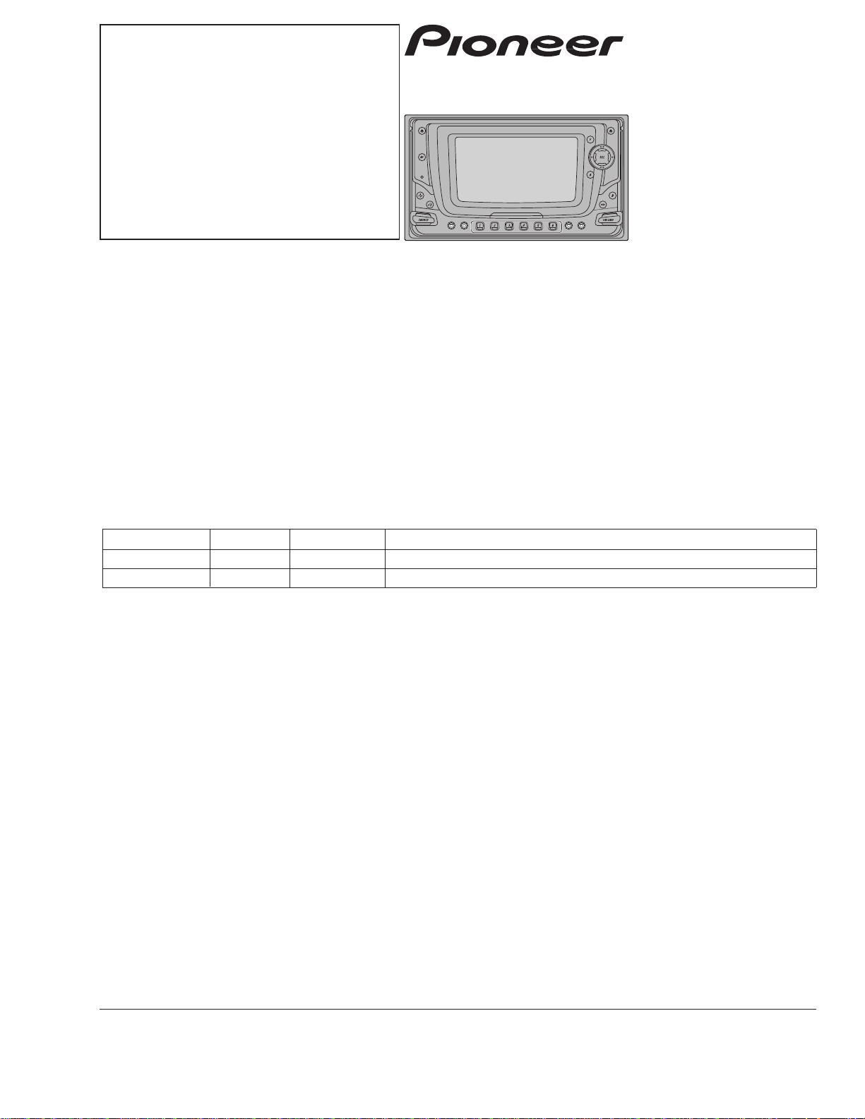
MULTI-CD/MD CONTROL DSP HIGH POWER CD CASSETTE PLAYER WITH RDS TUNER
FH-P6600R EW
FH-P6600R/EW
- This service manual should be used together with the following manual(s):
Model No. Order No. Mech. Module Remarks
CX-1011 CRT2406 3L Cassette Mech. Module:Circuit Description, Mech.Description, Disassembly
CX-958 CRT2423 S8.1 CD Mech. Module:Circuit Description, Mech.Description, Disassembly
CONTENTS
1. SAFETY INFORMATION ............................................2
2. EXPLODED VIEWS AND PARTS LIST.......................3
3. BLOCK DIAGRAM AND SCHEMATIC DIAGRAM ...16
4. PCB CONNECTION DIAGRAM ................................42
5. ELECTRICAL PARTS LIST ........................................60
6. ADJUSTMENT..........................................................78
7. GENERAL INFORMATION .......................................83
7.1 DIAGNOSIS ........................................................83
7.1.1 TEST MODE ..............................................83
7.1.2 DISASSEMBLY .........................................87
7.1.3 PCB LOCATIONS ......................................94
7.2 PARTS .................................................................95
7.2.1 IC................................................................95
7.2.2 DISPLAY..................................................106
7.3 OPERATIONAL FLOW CHART.........................108
8. OPERATIONS AND SPECIFICATIONS...................109
- Dolby noise reduction manufactured under license from Dolby Laboratories Licensing Corporation.
"Dolby" and the double-D symbol are trademarks of Dolby Laboratories Licensing Corporation.
- Three-color LEDs: The LCD backlight uses Hitachi's 3-color LEDs (NSCM315C) to control voltages for
RGB reproduction. By individually controlling the voltages for red, green and blue LEDs, these three
colors are mixed to reproduce ten colors.
FH-P6600
ES
MULTI-CD/MD CONTROL DSP HIGH POWER CD CASSETTE PLAYER WITH FM/AM TUNER
Page 2
2
FH-P6600R,P6600
- CD Player Service Precautions
1. For pickup unit(CXX1285) handling, please refer
to"Disassembly"(see page 87).
During replacement, handling precautions shall be
taken to prevent an electrostatic discharge(protection
by a short pin).
2. During disassembly, be sure to turn the power off
since an internal IC might be destroyed when a con-
nector is plugged or unplugged.
3. Please checking the grating after changing the ser-
vice pickup unit(see page 81).
1. SAFETY INFORMATION
This service manual is intended for qualified service technicians; it is not meant for the casual do-it-yourselfer.
Qualified technicians have the necessary test equipment and tools, and have been trained to properly and safely repair
complex products such as those covered by this manual.
Improperly performed repairs can adversely affect the safety and reliability of the product and may void the warranty.
If you are not qualified to perform the repair of this product properly and safely; you should not risk trying to do so
and refer the repair to a qualified service technician.
1. Safety Precautions for those who Service this Unit.
• When checking or adjusting the emitting power of the laser diode exercise caution in order to get safe, reliable
results.
Caution:
1. During repair or tests, minimum distance of 13cm from the focus lens must be kept.
2. During repair or tests, do not view laser beam for 10 seconds or longer.
2. A “CLASS 1 LASER PRODUCT” label is affixed to the
bottom of the player.
3. The triangular label is attached to the mechanism
unit frame.
4. Specifications of Laser Diode
Specifications of laser radiation fields to which human access is possible during service.
Wavelength = 800 nanometers
CLASS 1
LASER PRODUCT
Page 3
3
FH-P6600R,P6600
8
9
10
11
13
1
2
4
3
12
7
6
5
22
18
17
17
14
15
16
19
20
21
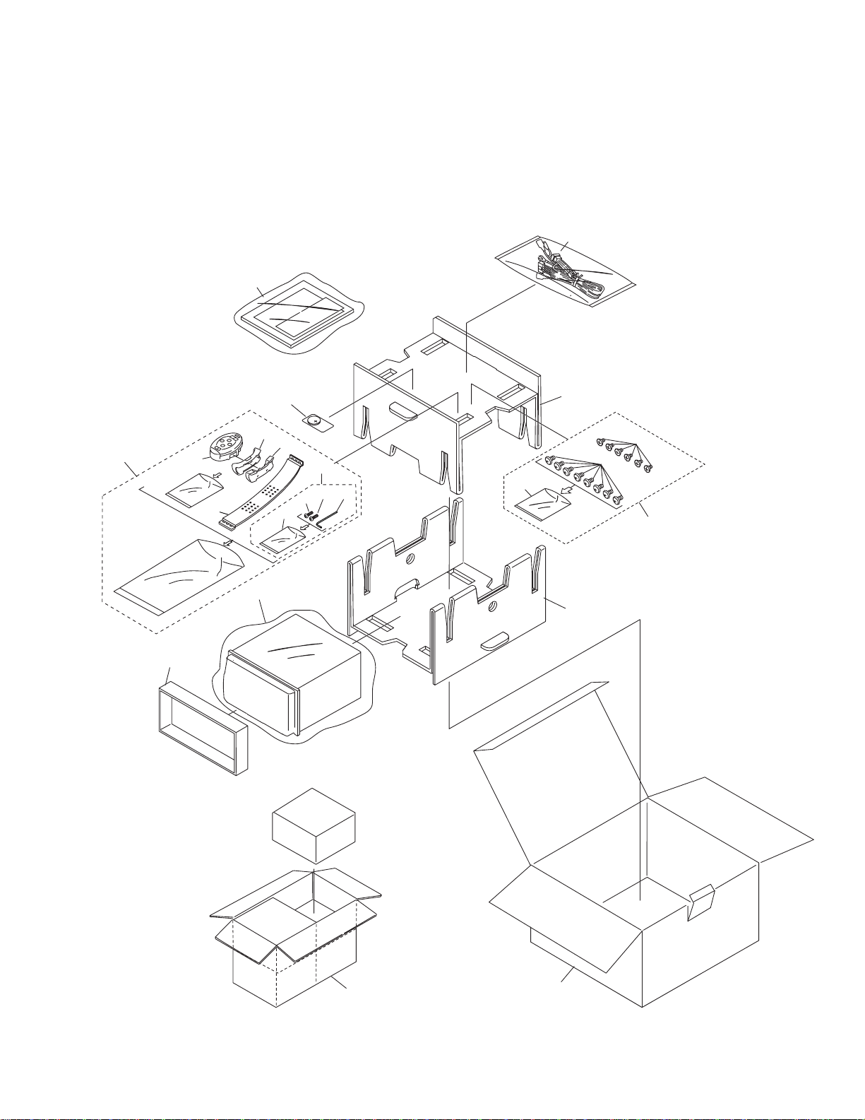
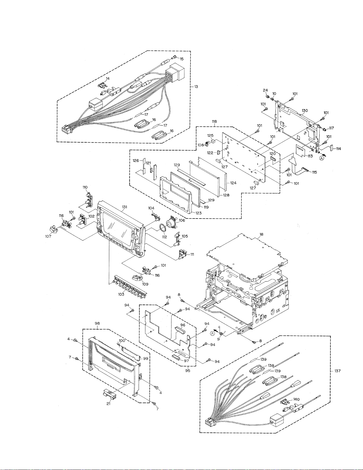
2. EXPLODED VIEWS AND PARTS LIST
2.1 PACKING(FH-P6600R/EW)
Page 4

4
FH-P6600R,P6600
- PACKING SECTION PARTS LIST
Mark No. Description Part No.
NOTE:
- Parts marked by "*"are generally unavailable because they are not in our Master Spare Parts List.
- Screws adjacent to ∇ mark on the product are used for disassembly.
1 Screw Assy CEA2189
2 Screw BMZ50P060FMC
* 3 Polyethylene Bag CEG-127
4 Screw CMZ50P060FMC
5 Cord Assy CDE6404
6-1 Polyethylene Bag CEG1116
6-2 Owner's Manual CRD3237
6-3 Owner's Manual CRD3238
6-4 Installation Manual CRD3239
6-5 Installation Manual CRD3240
6-6 Caution Card CRP1208
6-7 Passport CRY1013
* 6-8 Warranty Card CRY1157
7 Battery CEX1030
8 Carton CHG4056
9 Contain Box CHL4056
10 Cover CEG1074
11 Protector CHP2227
12 Protector CHP2272
13 Protector CHP2273
14 Screw Assy CZE3169
* 15 Polyethylene Bag CEG-127
* 16 Hexagonal Wrench CZE3176
* 17 Screw RMZ30H060FBK
18 Belt CZN6416
19 Holder Assy CZX3172
20 Holder Assy CZX3173
21 Remote Control Assy CZX3218
22 Remote Control Assy CXB2636
As materials for on-site adjustment, the following items are contained in the package:
CRD3237 (Owner's manual in English, Italian and Spanish) *A
CRD3239 (Installation manual in English, Italian and Spanish) *A
CRD3238 (Owner's manual in French, Dutch and German) *B
CRD3240 (Installation manual in French, Dutch and German) *B
When the products are shipped from our factory, the above manuals are not included. A
pair of manuals (*A or *B) will be attached to the product package on the site (PEE)
according to the language used in the country or area to which the product is delivered.
Page 5
5
FH-P6600R,P6600
8
9
10
11
13
1
2
4
3
12
17
18
14
5
16
15
7
6
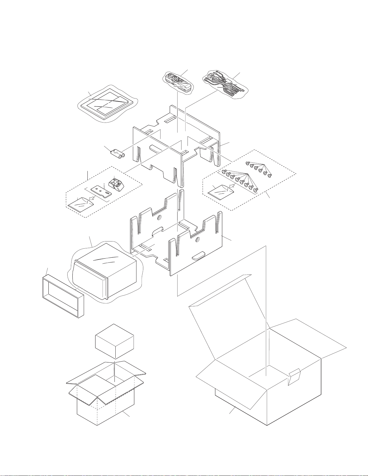
2.2 PACKING(FH-P6600/ES)
Page 6

6
FH-P6600R,P6600
1 Screw Assy CEA2189
2 Screw BMZ50P060FMC
* 3 Polyethylene Bag CEG-127
4 Screw CMZ50P060FMC
5 Polyethylene Bag CZE3188
6-1 Polyethylene Bag CEG1116
6-2 Owner’s Manual CRD3241
6-3 Installation Manual CRD3242
7 Battery CEX1006
8 Carton CHG4057
9 Contain Box CHL4057
10 Cover CEG1074
11 Protector CHP2227
12 Protector CHP2272
13 Protector CHP2273
14 Base Assy CEA2426
* 15 Base CNS5031
* 16 Sheet CZA3371
17 Cord Assy CDE6257
18 Remote Control Assy CXB3877
- PACKING SECTION PARTS LIST
Mark No. Description Part No.
Page 7
FH-P6600R,P6600
7
2.3 EXTERIOR
Page 8
8
FH-P6600R,P6600
Page 9

9
FH-P6600R,P6600
1 Screw BMZ26P060FMC
2 Screw BMZ26P250FMC
3 Screw BSZ26P060FMC
4 Screw BSZ30P060FMC
5 Screw BSZ30P080FMC
6 Screw BSZ30P160FMC
7 Screw(M2x2.5) CBA1085
8 Screw CBA1431
9 Spring CBH2092
10 Spring CBH2355
11 Cord CDE6262
12 Cable CDE6272
13 Cord Assy
See Contrast table(2)
14 Fuse(10A) See Contrast table(2)
15 Cap
See Contrast table(2)
16 Cap See Contrast table(2)
17 Resistor
See Contrast table(2)
18 Case CNB2556
19 Cover CNC8924
20 Heat Sink CNR1580
21 Cover CNS5007
22 Cap CNV2680
23 Holder CNV6248
24 Roller CNV6292
25 Cord CDE6260
26 Antenna Cable CDH1284
27 Holder CNC9006
28 Cushion CNM6893
29 Audio Amp Unit
See Contrast table(2)
30 Clamper CEF1007
31 Terminal(CN401) CKF1059
32 Plug(CN853) CKM1278
33 Connector(CN251) CKS2191
34 Connector(CN801) CKS3124
35 Connector(CN131) CKS3408
36 Plug(CN854) CKS3540
37 Connector(CN111) CKS3568
38 Connector(CN141) CKS4281
39 Connector(CN856) CKS4322
40 Connector(CN857) CKS4322
41 Pin Jack(CN451) CKX1046
42 Holder CNC7533
43 Holder CNC8724
44 Holder CNC8725
45 Holder CNC8727
46 Case CNC8873
47 Insulator CNM5967
48 •••••
49 Insulator
See Contrast table(2)
50 FM/AM Tuner Unit
See Contrast table(2)
51 Holder CNC7532
52 Power Supply Unit
See Contrast table(2)
53 Screw BMZ26P060FMC
54 Clamper CEF1007
55 Plug(CN901) CKS1242
56 Connector(CN902) CKS4321
57 Connector(CN903) CKS4321
58 Heat Sink CNR1579
59 Drive Mechanism Assy CXB5497
60 Screw BMZ20P025FMC
61 Screw BSZ30P060FMC
62 Screw(M2x2.5) CBA1521
63 Screw(M2x2.5) CBA1521
64 Washer CBF1038
65 Washer CBF1039
66 Spring CBL1493
67 Cord CDE6282
68 Bracket CNC8737
69 Spacer CNM6202
70 Insulator CNM6661
71 Spacer CNM6923
72 Gear CNV5297
73 Gear CNV5298
74 Guide CNV6291
75 Roller CNV5301
76 Roller CNV5814
77 Guide CNV6399
78 Gear CNV6164
79 Rack CNV5299
80 Rack CNV6149
81 Gear CNV6401
82 Chassis Unit CXB5319
83 Frame Unit CXB5321
84 Bracket Unit CXB5422
* 85 Motor CXM1114
86 Screw JFZ20P025FMC
87 Screw ISS26P055FUC
88 Screw BSZ26P060FMC
89 Insulator CNM6666
90 Clamper CNV1251
(1) EXTERIOR SECTION PARTS LIST
Mark No. Description Part No. Mark No. Description Part No.
Page 10

10
FH-P6600R,P6600
91 Clamper CNV6309
92 Chassis Unit CXB5420
93
Cassette Mechanism ModuleEXK4020
94 Screw BPZ20P080FMC
95 Panel PCB Unit
See Contrast table(2)
96 Socket(CN1101) CKS3553
97 Connector(CN1102) CKS3770
98 Panel Unit CXB5437
99 Door CAT2150
100 Spring CBH1371
101 Screw BPZ20P080FMC
102 Button(ANGLE) CAC6533
103 Button(1-6,etc) CAC6534
104 Button(EJECT) CAC6535
105 Button(F,A) CAC6537
106 Button(SEL) CAC6538
107 Lever(SOURCE) CAC6539
108 IC(IC1903) SBX8035-H
109 Lever(VOLUME) CAC6540
110 Button(CD EJ) CAC6541
111 Button(DSP,BAND) CAC6542
112 Cushion CNM6646
113 Insulator CNM6647
* 114 Cushion CNM6938
115 PCB CNP5309
116 Holder CNV6136
117 Roller CNV6172
118 Flap PCB Unit
See Contrast table(2)
119 LCD(LCD1901) CAW1593
120 Connector(CN1901) CKS3774
121 Connector(CN1201) CKS4274
122 Connector(CN1902) CKS4275
123 Holder CNC8699
124 Sheet CNM6642
125 Spacer CNM6644
126 Insulator CNM6719
127 Spacer CNM6940
128 Lighting Conductor CNV6133
129 Connector CNV6135
130 Case Unit CXB5262
131 Grille Unit
See Contrast table(2)
132
CD Mechanism Module(S8TX)
CXK5210
133 Remote Control Assy
See Contrast table(2)
134 Cover See Contrast table(2)
135 Remote Control Assy
See Contrast table(2)
136 Battery Cover See Contrast table(2)
137 Cord Assy See Contrast table(2)
138 Cap See Contrast table(2)
139 Resistor See Contrast table(2)
140 Fuse(10A) See Contrast table(2)
141 IC(IC351) PAL005A
142 IC(IC903) SBX8035-H
143 IC9IC907) PQ20RX1S-L
144 Transistor(Q912,Q915,Q921) 2SD2396
145
Cushion CNM6870
146 Cushion CNM6997
147 Spacer CNM7014
Mark No. Description Part No. Mark No. Description Part No.
Page 11

11
FH-P6600R,P6600
Part No.
Mark No. Symbol and Description FH-P6600R/EW FH-P6600/ES
13 Cord Assy CDE6404 Not used
14 Fuse(10A) CEK1136 Not used
15 Cap CKX-003 Not used
16 Cap CNS1472 Not used
17 Resistor RS1/2PMF102J Not used
29 Audio Amp Unit CWM7006 CWM7001
49 Insulator CNM6034 Not used
50 FM/AM Tuner Unit CWE1500 CWE1501
52 Power Supply Unit CWM7007 CWM7002
95 Panel PCB Unit CWM7008 CWM7003
118 Flap PCB Unit CWM7009 CWM7004
131 Grille Unit CXB6482 CXB6483
133 Remote Control Assy CZX3218 Not used
134 Cover CZN6410 Not used
135 Remote Control Assy Not used CXB3877
136 Battery Cover Not used CNS5032
137 Cord Assy Not used CDE6257
138 Cap Not used CNS1472
139 Resistor Not used RS1/2PMF102J
140 Fuse(10A) Not used CEK1136
(2) CONTRAST TABLE
FH-P6600R/EW and FH-P6600/ES are constructed same except for the following:
Page 12
12
FH-P6600R,P6600
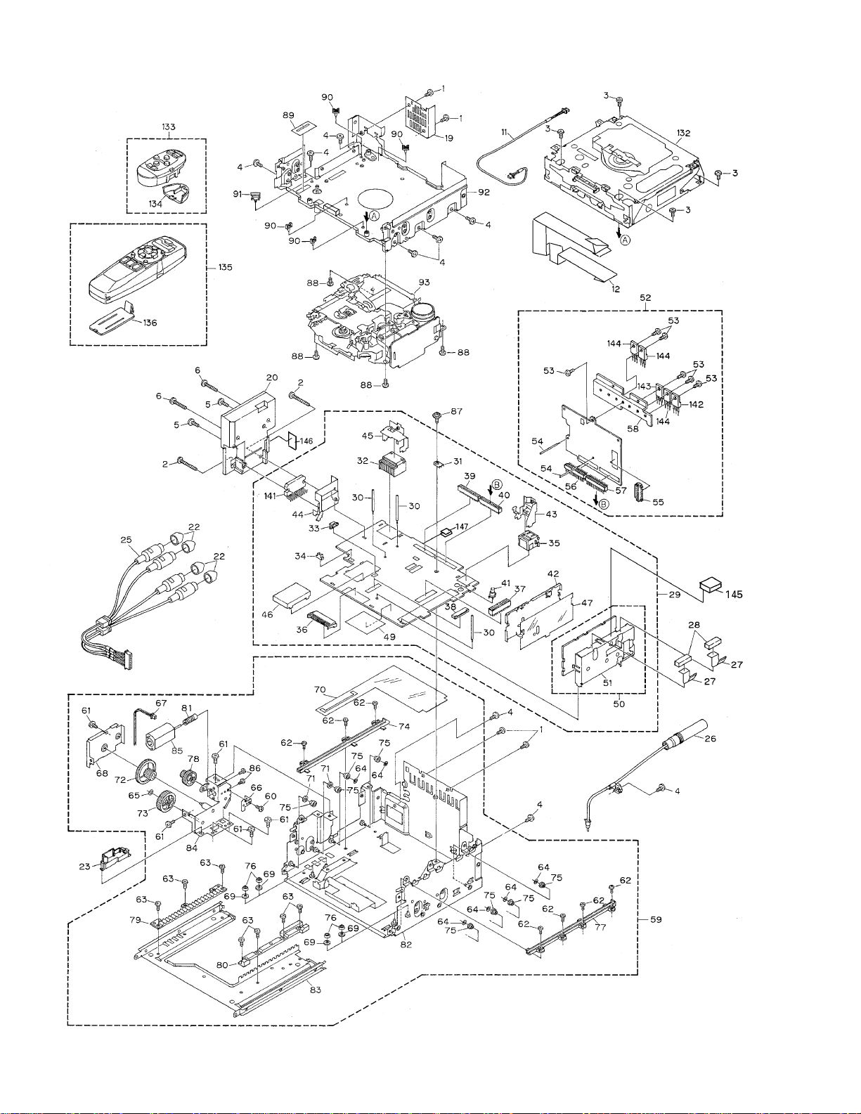
2.4 CD MECHANISM MODULE
Page 13

13
FH-P6600R,P6600
- CD MECHANISM MODULE SECTION PARTS LIST
1 Control Unit(S8TX) CWX2434
2 Connector(CN802) CKS2192
3 Connector(CN801) CKS2193
4 Connector(CN701) CKS4281
5 Connector(CN101) CKS3486
6 Screw BMZ20P030FMC
7 Screw BSZ20P040FMC
8 Screw(M2x3) CBA1077
9 Screw(M2x5) EBA1028
10 Screw(M2x2) CBA1523
11 Screw(M2x4) CBA1362
12 Washer CBF1037
13 Washer CBF1038
14 Washer CBF1060
15 •••••
16 Spring CBH2079
17 Spring CBH2117
18 Spring CBH2314
19 Spring CBH2110
20 Spring CBH2282
21 Spring CBH2318
22 •••••
23 Spring CBH2324
24 Spring CBH2118
25 Spring CBH2161
26 Spring CBH2163
27 Spring CBH2189
28 Spring CBH2249
29 Spring CBH2260
30 Spring CBH2262
31 Bracket CNC8568
32 Spring CBL1369
33 Connector CDE5531
34 Connector CDE5532
35 Shaft CLA3304
36 Screw(M2.6x6) CBA1458
37 Frame CNC8682
38 Frame CNC8892
39 Lever CNC8694
40 Arm CNC8663
41 Bracket CNC8567
42 •••••
43 Spacer CNM3315
44 Sheet CNM6659
45 •••••
46 •••••
47 Ball CNR1189
48 Belt CNT1086
49 Roller CNV4509
50 Arm CNV6102
51 Arm CNV6094
52 Arm CNV5248
53 Arm CNV6095
54 Guide CNV5254
55 Guide CNV5255
56 Gear CNV5257
57 Gear CNV5256
58 Guide CNV6176
59 Damper CNV6010
60 Arm CNV6096
61 Arm CNV6031
62 Arm CNV6211
63 Guide CNV6012
64 Guide CNV5510
65 •••••
66 Guide CNV5751
67 Clamper CNV6013
68 Gear CNV5813
69 Motor Unit(M1) CXB5827
70 Screw Unit CXB4726
71 Chassis Unit CXB5811
72 Gear Unit CXB4728
* 73 Arm Unit CXB5753
74 Motor Unit(M2) CXB5828
75 Lever Unit CXB6049
76 Arm Unit CXB4731
77 Motor Unit(M3) CXB5829
78 Arm Unit CXB5689
79 Bracket Unit CXB4795
80 Screw JFZ20P025FMC
81 Screw JGZ17P025FZK
82 Washer YE20FUC
83 Pickup Unit(Service)(P8) CXX1285
84 Screw IMS26P030FMC
* 85 Gathering PCB CNX2982
86 Photo Transistor(Q1, 2) CPT230SX-TU
87 Damper CNV6011
88 Rack CNV6014
89 Spring CBH2315
90 Connector(CN601) CKS4282
91 Connector(CN602) CKS2191
Mark No. Description Part No. Mark No. Description Part No.
Page 14

14
FH-P6600R,P6600
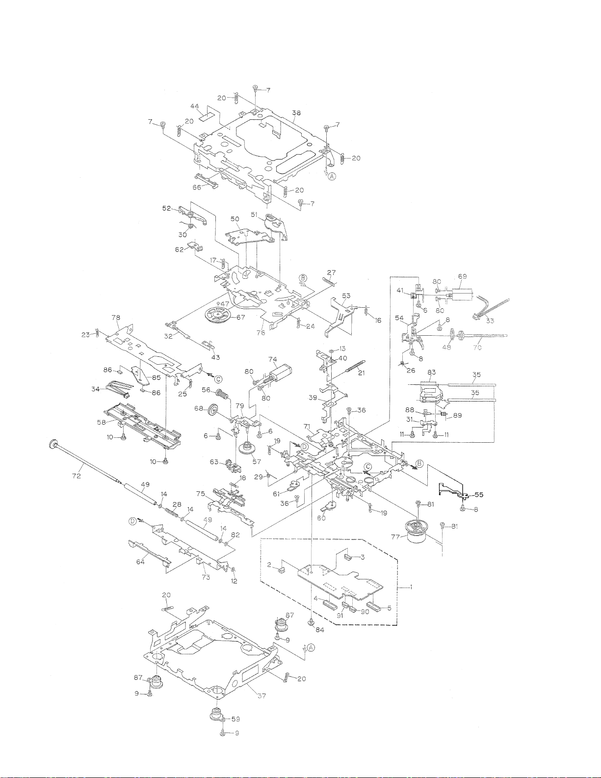
2.5 CASSETTE MECHANISM MODULE
Page 15

15
FH-P6600R,P6600
- CASSETTE MECHANISM MODULE SECTION PARTS LIST
1 Screw BSZ20P040FMC
2 Washer CBF1037
3 Washer CBG1003
4 Screw EBA1028
5 Screw CBA1037
6 Spring EBH1531
7 Spring EBH1624
8 Spring EBH1625
9 Spring EBH1626
10 Spring EBH1627
11 Spring EBH1629
12 Cord EDD1024
13 Photo-reflector(EGN1) EGN1004
14 Arm ENC1526
15 Lever ENC1530
16 Lever ENC1531
17 Arm ENC1532
18 Frame ENC1533
19 Holder ENC1534
20 Gear ENC1535
21 Arm ENC1536
22 Roller ENR1040
23 Belt ENT1027
24 Collar ENV1508
25 Arm ENV1539
26 Arm ENV1540
27 Gear ENV1544
28 Gear ENV1547
29 Gear ENV1548
30 Worm Wheel ENV1550
31 Lever ENV1551
32 Flywheel ENV1554
33 Gathering PCB ENX1054
34 Switch(S1,S2,S3) ESG1007
35 Deck Unit EWM1029
36 Plug(CN251) CKS3540
37 PCB ENP1184
38 Motor Unit(M1) EXA1490
39 Motor EXM1027
40 Head Assy(HD1) EXA1589
41 Motor Unit(M2) EXA1580
42 Screw BMZ20P022FMC
43 Bracket ENC1528
44 Chassis Unit EXA1582
45 Pinch Holder Unit EXA1584
46 Pinch Roller ENV1518
47 Pinch Holder Unit EXA1583
48 Pinch Roller ENV1518
49 Reel Unit EXA1585
50 Head Base Unit EXA1586
51 Lever Unit EXA1587
52 Gear Unit EXA1588
53 Motor Unit(Service) EXX1055
54 Washer HBF-179
55 Screw CBA1250
56 Bracket ENC1542
57 Arm ENC1537
Mark No. Description Part No. Mark No. Description Part No.
Page 16
16
A
1
234
B
C
12
34
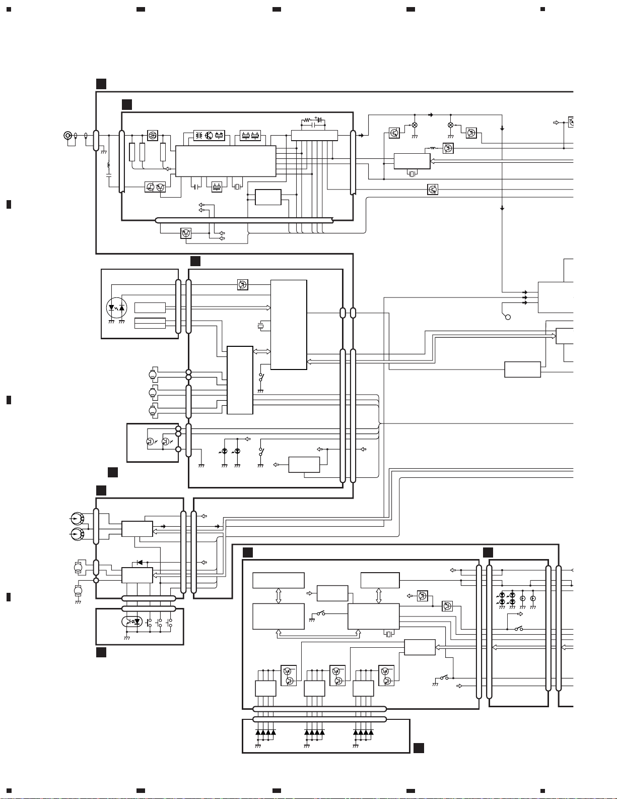
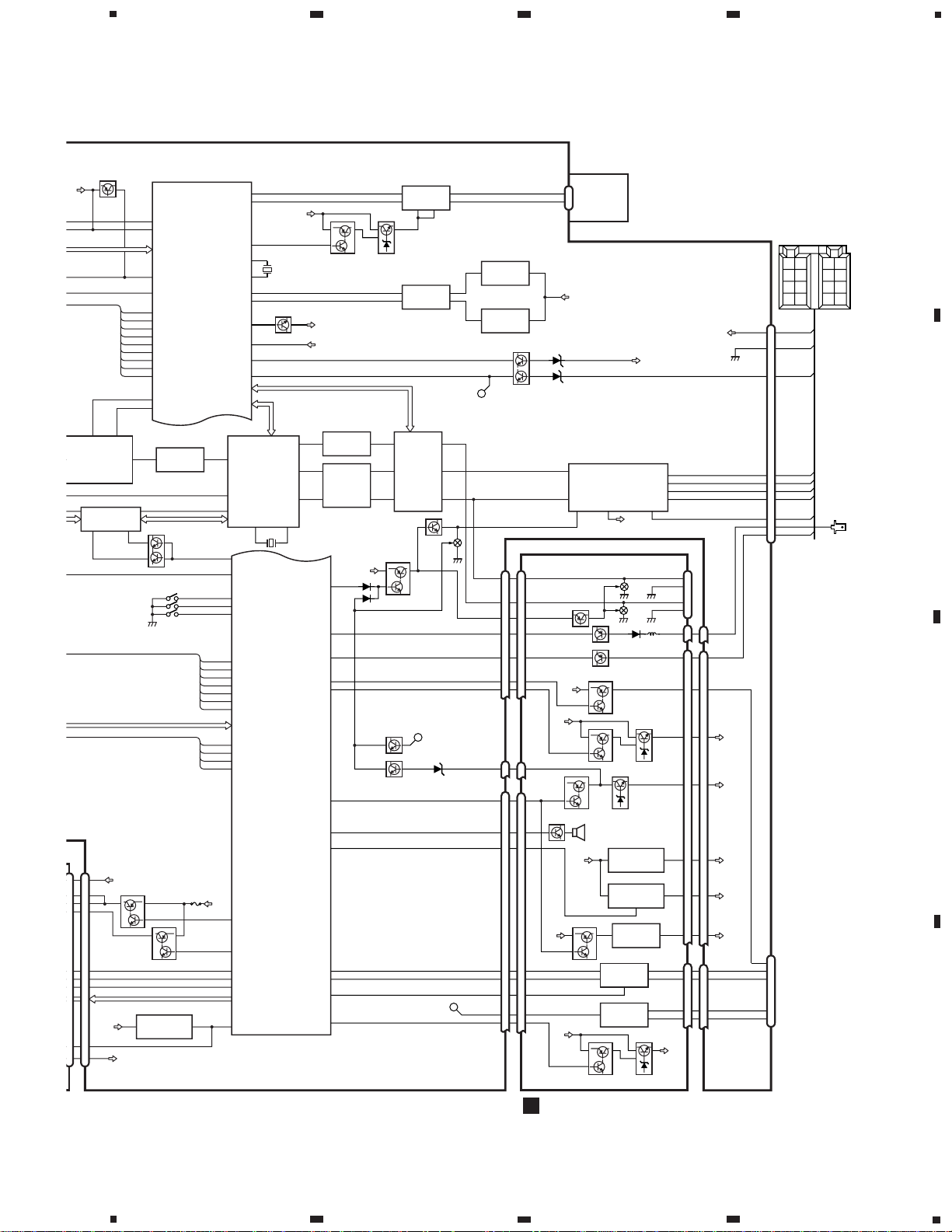
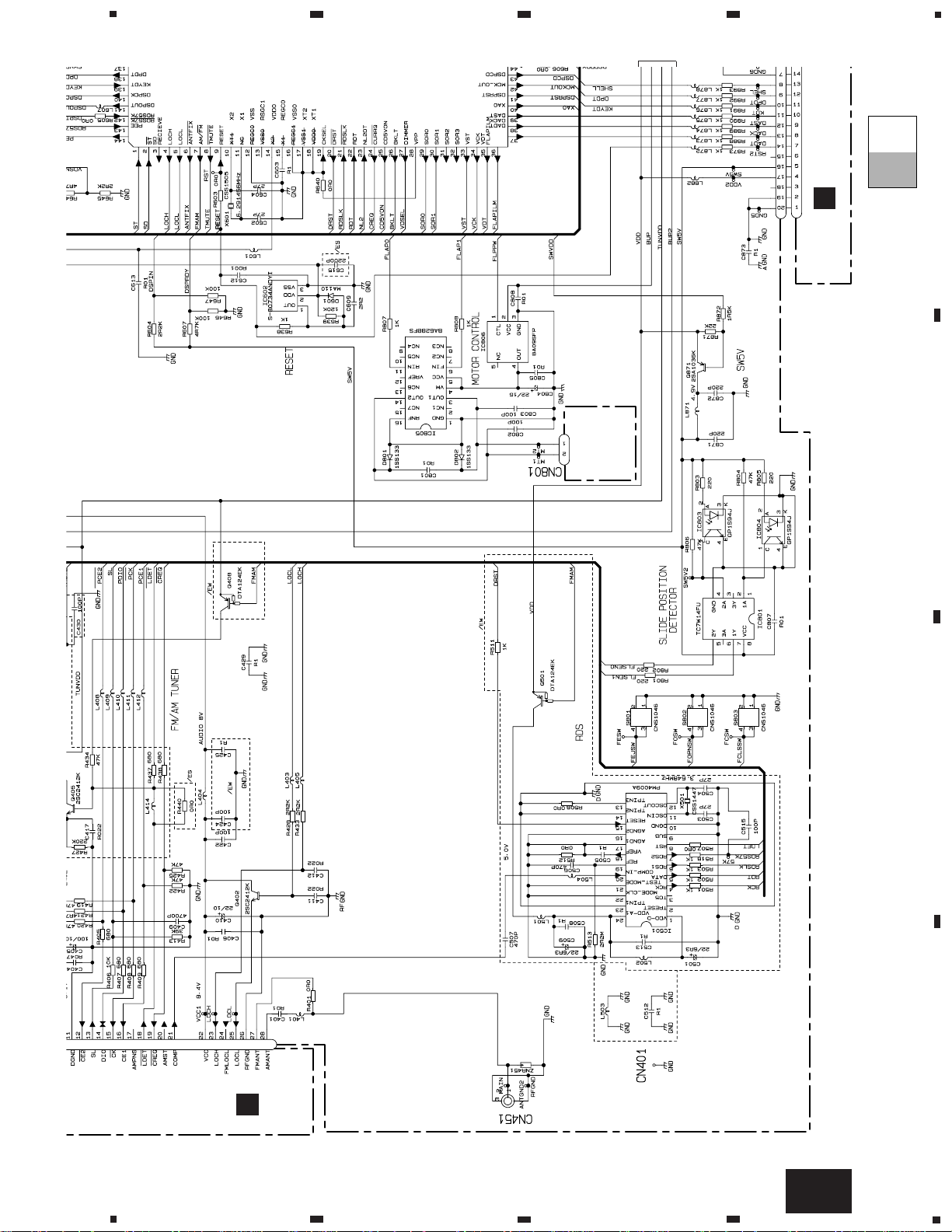
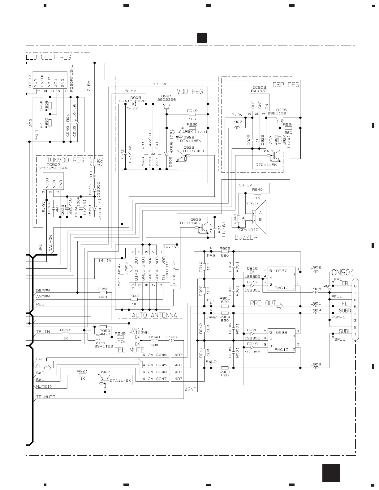
3. BLOCK DIAGRAM AND SCHEMATIC DIAGRAM
3.1 BLOCK DIAGRAM(EW model)
FH-P6600R,P6600
B
FM/AM TUNER UNIT
A
AUDIO AMP UNIT
CN451
RDS
DECODER
CDVD
CDLOAD
CDEJET
CONT
EJTSNS
DSCSNS
CLAMP
CD5VON
CDLOAD
CDEJET
CONT
EJS
DCS
CLAMP
CD5VON
G
CONTROL UNIT(S8TX)
H
PHOTO UNIT(S8)
Q401
X501
3.648MHz
Q405
Q501
Q407
Q403 Q406
8
11 12
20
24
8
10
9
2
1
+IN2A
SW1
20
4
+IN2C
16
+IN2B
18
4
18
21
6
NL2
ldet
COMP
L-OUT
IC 501
PM4009A
Q3
CF202
X901
VDD
VCC
LOCL
VDD
VCC
ANTENNA
27
28
1
2
Q201 Q204
T51 Q51 CF51 CF52 CF53
ANT1 TV
ANT2 TV
RF TV
AM RF
EEPROM
IC 3
BR9010FV
MIXER, IF AMP DET
IC 1
PML002A
FM/AM 1ST IF 10.7MHz
AM 2ND IF 450kHz
FM FRONT END
5
6
4
3
35
33
38 42 46
32
4439
45 55 57 61 74 75
71
65
78
54
70
69
63
25 24
19
46131211444134 33
22
IC 2 PM4008A
22 10 14 12 15 16 13 2 3
DI/DO
CE2CKCE1SLFMSD
NL1
IC 151
BA3131FS
ELECTRONIC VOLUME/
SOURCE SELECTOR
Q401
25
Q4
BUP
B
SELECT
SENSE
DISC SENSE
D802 D801
S802
CLAMP
LD
L_OUT
PD
HOME
RF-AMP, DSP,
SERVO, DAC
IC 201
UPD63711GC
IC 301
BA5985FM
12
16
18
11
14
13
10
9
SOP
TOP
FOP
SOM
COP
COM
LOP
LOM
FWD
REV
MUTE
CD DRIVER
XTAL
LASER
DIODE
MONITOR
DIODE
FOCUS ACT.
TRACKING ACT.
LD+
MD
F+
T+
14
19
4
3
PICKUP UNIT (SERVICE)(P8)
HOLOGRAM
UNIT
Q101
M
M
M
SPINDLE
MOTOR
CARRIAGE
MOTOR
LOADING
MOTOR
TD/FD
SD/MD
24
97
MCK MCK
LRCK
98
24
1
28
21
16
23
39
X201
CN701
CN602 CN251
CN141
1
8
22
23
21
24
7
6
5
11
1
15
29
30
28
31
14
13
12
18
S801
HOME
CN101
1
2
3
4
CN801
3
1
2
CN802
VD
IC 701
BA05SFP
42
1
VD
VDD
IC
TC74VH
IC 253
TC7SET08FU
M
M
CN252
CN254
CN255
CN256
CN253
CN251 CN111
DOLBY B
EQ AMP
MECHANISM
DRIVER
1
64513
64513
5
6
2
1
S3
70 sS1LOAD
S2
MODE
EGN1
REEL
SENSE
M1
MAIN
MOTOR
M2
SUB
MOTOR
REV
L-ch
FWD
L-ch
8710
1
2
5
TAPE+B
VCC
B.U
Lch
CCL
MUTE
B.U
stby
mtl
LOAD
MTL
LD
STBY
RIMUTE
1718
39
36
37
17
1918
7
5
IC 251
HA12216F
IC 351
PA2020A
J
REEL SENSE PCB
I
DECK UNIT
S1101
DOOR SENSE
S1945
RESET SW
1
2
3
4
8
9
10
14
20
19
18
17
13
12
11
7
174
11
ILM+B
LED+B
BKLT+B
BKLT+B
LED+B
LED+B
SWVDD
DISPdtIN
KEYdtOUT
RESET
VDD
ILM+B
FLPILM+B
SHELL
DPDT
KYDT
RESET
VDD
SW5V
KEY MATRIX
Q1930
Q1920
SW5V
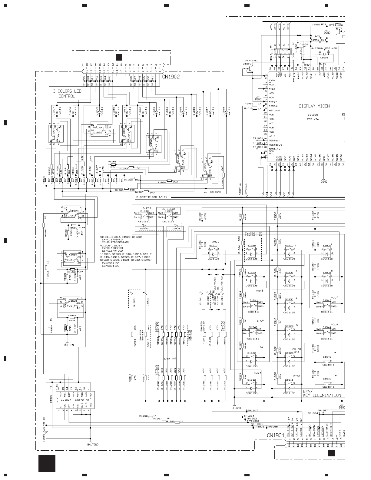
IC 1904
M62361FP
DISPLAY MIC
IC 1905
PE5149A
LCD DRIVER
IC 1901
SED1526F0A
LCD
RO COMPUTER
3 COLOR LED
LED
DRIVE
Q1923
Q1925,
Q1928
LED
DRIVE
Q1922
Q1926,
Q1929
LED
DRIVE
Q1921
Q1924,
Q1927
+5V REGULATOR
4
3
9
20
19
8
11
4
3
9
20
19
8
11
CN1101 CN85CN1901 CN1102
CN1902
CN1201
VDD
10
12
13
27
19
20
25
28
2
1
3
4
18
10
11
16
19
15 14 5 2 16 13 7 3 17 12 6 4
15 14 5 2 16 13 7 3 17 12 6 4
50
31
61
63
15
14
13
8
9
60
VDD
S1939 CDEJET
X1901
70 69
IC 1903
SBX8035-H
REM
VCC
D
FLAP PCB
E
LED PCB
F
PANEL PCB UNIT
D
Page 17
17
FH-P6600R,P6600
5
6
7
8
5
6
7
8
A
B
C
D
BUP
8
10 4
9
9
FLAP1
CDVD
BUP
85
FLAP0
84
FLAPPW
86
bsens
96
asens
97
VDSENS
112
FLIN
RLIN
SYSPW
12
14
22 4 25
OUT2
14
8
RL—
23
RL+
21
FL—
3
FL+
RL—
ACC
GND
BUP
BUP
BUP
RL+
FL—
BREM
FL+
FL
SUBL
5
SW1 SW2
1
336
SL
106
NL1
107
126
TUNPCE
129
TUNPCK
125
TUNPDO
127
TUNPDI
LOCL
5
SOR0
29
SOR1
30
TUNPCE2
128
SD
2
NL2DT
23
ldet
101
FM/am
7
tmute
8
IC 151
BA3131FS
IC 351
PAL005A
LUME/
POWER AMP
SLIDE POSITION SENSE
SYSTEM
MICRO COMPUTER
IC 601 (1/2)
PE5124A
MUTE STBY B.REM
Q871
Q802
Q408
Q803
Q801
Q931
Q932
2
1
5
9
11
10
12
4
ILL
RL—
ACC
GND
BUP
RL+
FL—
BREM
FL+
ILL
3
TELMUTE
8
CN853
A
IC 805
BA6288FS
11
6
14
13
54
MT2
MT1
1
2
CN801
MOTOR
UNIT
X2
10
X1
11
X601
6.291456MHz
SWVDD
137
FLSEN1
116
FLSEN0
115
IC 801
TC7W14FU
7
5
2
4
IC 804
GP1S94J
12
IC 803
GP1S94J
12
SW5V
VDD
IC 153
NJM4558MD
LIN
58
BFOT
76
LRCK
DSP
IC 251
PDG255A
IC 303
NJM4558MD
57
IC 304
NJM4558MD
31
57
619
718
817
AOUTL2
39
AOUTL3
52
AOUTL1
27
IC 301
PM0017AM
IC 252
TC74VHC125FT
MCK_OUT
42
DSPMS
131
RIMUTE
LOADSW
MTLSW
STBY
76
75
70
71
ILMPW
77
SHEEL
94
DPDT
138
KEYDT
139
RESET
9
flapejsw
114
fopnsw
82
fclssw
83
Q251
S801 FEJSW
S802 FOPNSW
S803 FCLSSW
Q854
Q853
Q351
XTALI38
42
XTALO38
41
X251
16.9344MHz
BUP
Q852
A
Q352
Q937
1
1
CN857
1
5
6
2
CN901
CN903
CN903 CN857
Q938
Q927
Q935
Q936
BUP
Q916
Q917
Q915
BUP
Q932
Q931
Q851
Q913
Q914
Q912
Q933
BZ901
ALARM
BUZZER
BUP
Q926
Q925
3
2
IC 902
S-81250SGUP
3
2
1
IC 907
PQ20RX1S-L
3
1
IC 903
BA033T
IC 904
CA0008AM
1
2
6
5
5
IC 905
TA2050F
1
12
14
BUP
Q922
Q923
Q921
8
1
5
7
11
CN131
CDVD
A8V
TUNVDD
LED+8
A3V
BUSL2
BUSL1
BUS—
BUS+
ASENB
ILL
VDD
CDLOAD
CONT
SDEJECT
59
58
55
EJTSNS
CLAMP
DSCSNS
110
111
54
CD5VON
25
Q872
Q874
Q875
FLAPILM
36
BUP
1
2
3
4
8
9
10
14
20
19
18
17
13
12
11
7
174
LED+B
IC 602
S-80734ANDYI
2
1
VDD
MUTE
FL
SWL
MUTE
TELIN
ISENS
ASENBO
VDCNTCD
MUTE
SYSPW
PEE
BKLT
TX
RX
IPPW
IPL
DALMON
79
TEL_IN
117
isens
98
ASENBO
87
VDCONT
56
SYSPW
80
PEE
144
BKLT
26
TX
89
RX
90
IPPW
88
DALMON
81
16
15
27
23
30
29
6
16
15
27
23
30
29
6
28
28
CN902 CN856
30
30
28
28
13
13
10
10
17
17
14
14
11
11
CN903 CN857
13
9
9
24
24
14
14
13
CN856
CN902
18
18
CN857 CN903
2
2
3
3
7
7
8
8
25
25
10
10
12
12
5
5
B
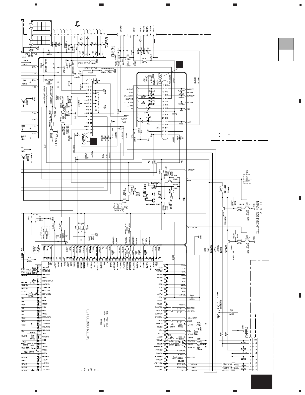
SYSTEM
MICRO COMPUTER
IC 601 (2/2)
PE5124A
RESET
CN854
C
POWER SUPPLY UNIT
TELMUTE
ILL
ASEN(IP)
CD+B
SYS+B
TU5V
LED+B
DSP+B
BUS+
BUS—
L+
L—
DSP
MIX
E VOL
CD
REG.
SYS
REG.
TUNVDD REG.
LED REG.
DSP REG.
IP-DRIVER
IP ISOLATOR
RCA
IP-BUS
FL
+
RL
+
RR
+
RL
+
FL
—
RL
—
RR
—
RL
—
ACC
ANT
GND
ILL
BACK
UP
Page 18
18
FH-P6600R,P6600
A
1
234
B
C
D
12
34
CN701
CN602
CONTROL UNIT
FM/AM TUNER UNIT
I
CN251
ANTENNA
MOTOR
UNIT
G
B
FM(100%)EW :-15.5dBs
FM(100%)ES :-19.5dBs
AM(30%)EW :-26dBs
AM(30%)ES :-30dBs
IP-BUS :+1.2dBs
TAPE :-12.8dBs
TAPE :-9dBs
FM(100%)EW :-15.5dBs
FM(100%)ES :-19.5dBs
AM(30%)EW :-26dBs
AM(30%)ES :-30dBs
A
A-aA-a A-b A-b
A-aA-a
A-b A-b
A-b A-b
A-a A-a
Large size
SCH diagram
Guide page
Detailed page
A-a
3.2 OVERALL CONNECTION DIAGRAM(GUIDE PAGE)
Note: When ordering service parts, be sure to refer to “EXPLODED VIEWS AND PARTS LIST” or “ELECTRICAL
PARTS LIST”.
Page 19
FH-P6600R,P6600
5
6
7
8
A
B
C
D
5
6
7
8
19
CN1101
Decimal points for resistor
and capacitor fixed values
are expressed as :
2.2 2R2
0.022 R022
←
←
The > mark found on some component parts indicates
the importance of the safety factor of the part.
Therefore, when replacing, be sure to use parts of
identical designation.
Symbol indicates a resistor.
No differentiation is made between chip resistors and
discrete resistors.
NOTE :
Symbol indicates a capacitor.
No differentiation is made between chip capacitors and
discrete capacitors.
>
>
>
PANEL PCB UNIT
C
CN902
C
CN903
IP-BUS
F
AUDIO AMP UNIT
A
FL
+
RL
+
RR
+
RL
+
FL
—
RL
—
RR
—
RL
—
ACC
ANT
GND
ILL
BACK
UP
EW
s
s
Bs
FM(100%)EW :-0.8dBs
FM(100%)ES :-4.8dBs
AM(30%)EW :-11.3dBs
AM(30%)ES :-15.3dBs
IP-BUS :+1.2dBs
TAPE :-12.8dBs
FM(100%)EW :-6.8dBs
FM(100%)ES :-10.8dBs
AM(30%)EW :-17.3dBs
AM(30%)ES :-21.3dBs
IP-BUS :-4.8dBs
TAPE :-18.8dBs
FM(100%)EW :-4.4dBs
FM(100%)ES :-8.4dBs
AM(30%)EW :-14.9dBs
AM(30%)ES :-18.9dBs
IP-BUS :-2.4dBs
CD :-1.4dBs
TAPE :-16.4dBs
FM(100%)EW :+3.2dBs
FM(100%)ES :-0.8dBs
AM(30%)EW :-7.3dBs
AM(30%)ES :-11.3dBs
IP-BUS :+5.2dBs
CD :+6.2dBs
TAPE :-8.8dBs
FM(100%)EW :+8.2dBs
FM(100%)ES :+4.2dBs
AM(30%)EW :-2.3dBs
AM(30%)ES :-6.3dBs
IP-BUS :+10.2dBs
CD :+11.2dBs
TAPE :-3.8dBs
FM(100%)EW :+34.2dBs
FM(100%)ES :+30.2dBs
AM(30%)EW :+23.7dBs
AM(30%)ES :+19.7dBs
IP-BUS :+36.2dBs
CD :+37.2dBs
TAPE :+22.2dBs
IP-BUS :+2.2dBs
A
A-b
Page 20
20
FH-P6600R,P6600
CN701
CN602
CONTROL UNIT
UNIT
I
CN251
G
FM(100%)EW :-15.5dBs
FM(100%)ES :-19.5dBs
AM(30%)EW :-26dBs
AM(30%)ES :-30dBs
IP-BUS :+1.2dBs
TAPE :-12.8dBs
TAPE :-9dBs
FM(100%)EW :-15.5dBs
FM(100%)ES :-19.5dBs
AM(30%)EW :-26dBs
AM(30%)ES :-30dBs
A
1
234
B
C
D
1
2
34
A-a
A-b
A-a
1
2
3
4
Page 21
21
FH-P6600R,P6600
FM/AM TUNER UNIT
PANEL PCB UN
ANTENNA
MOTOR
UNIT
F
B
5
6
7
8
A
B
C
D
5
6
7
8
A-a
A-b
A-a
5
6
Page 22
22
FH-P6600R,P6600
AUDIO AMP UNIT
A
RRRR
EW
FM(100%)EW :-0.8dBs
FM(100%)ES :-4.8dBs
AM(30%)EW :-11.3dBs
AM(30%)ES :-15.3dBs
IP-BUS :+1.2dBs
TAPE :-12.8dBs
FM(100%)EW :-6.8dBs
FM(100%)ES :-10.8dBs
AM(30%)EW :-17.3dBs
AM(30%)ES :-21.3dBs
IP-BUS :-4.8dBs
TAPE :-18.8dBs
FM(100%)EW :-4.4dBs
FM(100%)ES :-8.4dBs
AM(30%)EW :-14.9dBs
AM(30%)ES :-18.9dBs
IP-BUS :-2.4dBs
CD :-1.4dBs
TAPE :-16.4dBs
FM(100%)EW :+3.2dBs
FM(100%)ES :-0.8dBs
AM(30%)EW :-7.3dBs
AM(30%)ES :-11.3dBs
IP-BUS :+5.2dBs
CD :+6.2dBs
TAPE :-8.8dBs
FM(100%)EW :+8.2dBs
FM(100%)ES :+4.2dBs
AM(30%)EW :-2.3dBs
AM(30%)ES :-6.3dBs
IP-BUS :+10.2dBs
CD :+11.2dBs
TAPE :-3.8dBs
FM(100%)EW :+34.2dBs
FM(100%)ES :+30.2dBs
AM(30%)EW :+23.7dBs
AM(30%)ES :+19.7dBs
IP-BUS :+36.2dBs
CD :+37.2dBs
TAPE :+22.2dBs
A
1
234
B
C
D
12
34
A-a
A-b
A-b
1
2
3
4
Page 23
23
FH-P6600R,P6600
CN1101
Decimal points for resistor
and capacitor fixed values
are expressed as :
2.2 2R2
0.022 R022
←
←
The > mark found on some component parts indicates
the importance of the safety factor of the part.
Therefore, when replacing, be sure to use parts of
identical designation.
Symbol indicates a resistor.
No differentiation is made between chip resistors and
discrete resistors.
NOTE :
Symbol indicates a capacitor.
No differentiation is made between chip capacitors and
discrete capacitors.
>
>
>
C
CN902
C
CN903
IP-BUS
FL
+RL+RR+
RL
+
FL
—RL—RR—
RL
—
ACC
ANT
GND
ILL
BACK
UP
EW
IP-BUS :+2.2dBs
5
6
7
8
A
B
C
D
5
6
7
8
A-a
A-b
A-b
5
6
Page 24
24
FH-P6600R,P6600
A
1
234
B
C
D
12
34
B
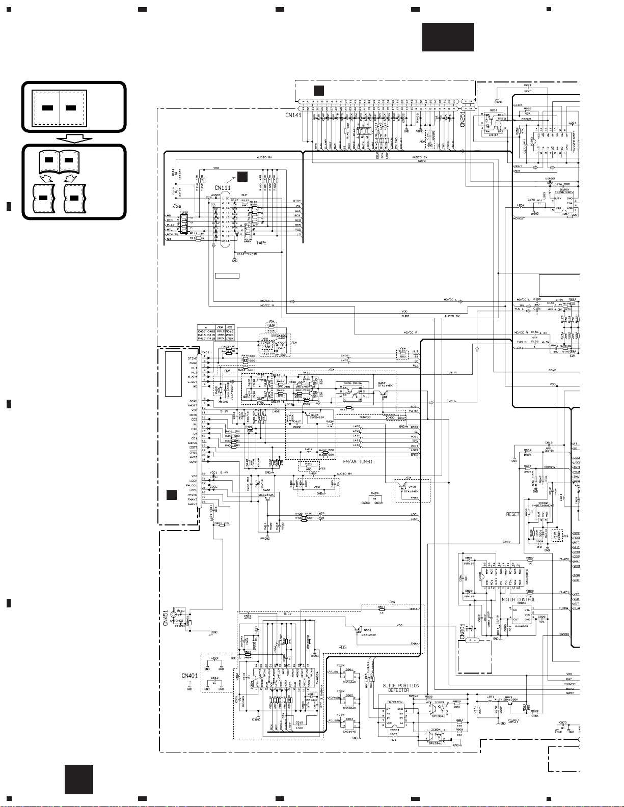
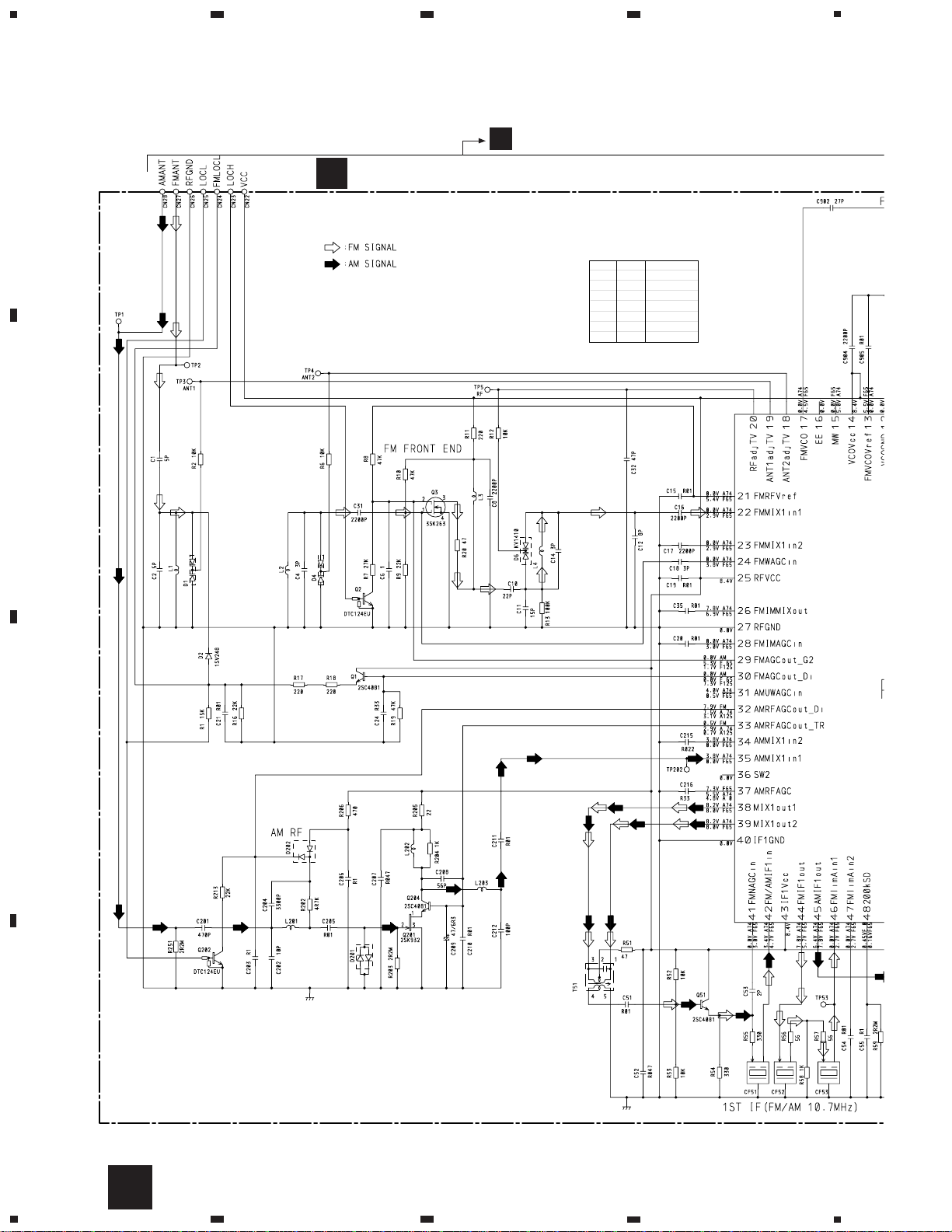
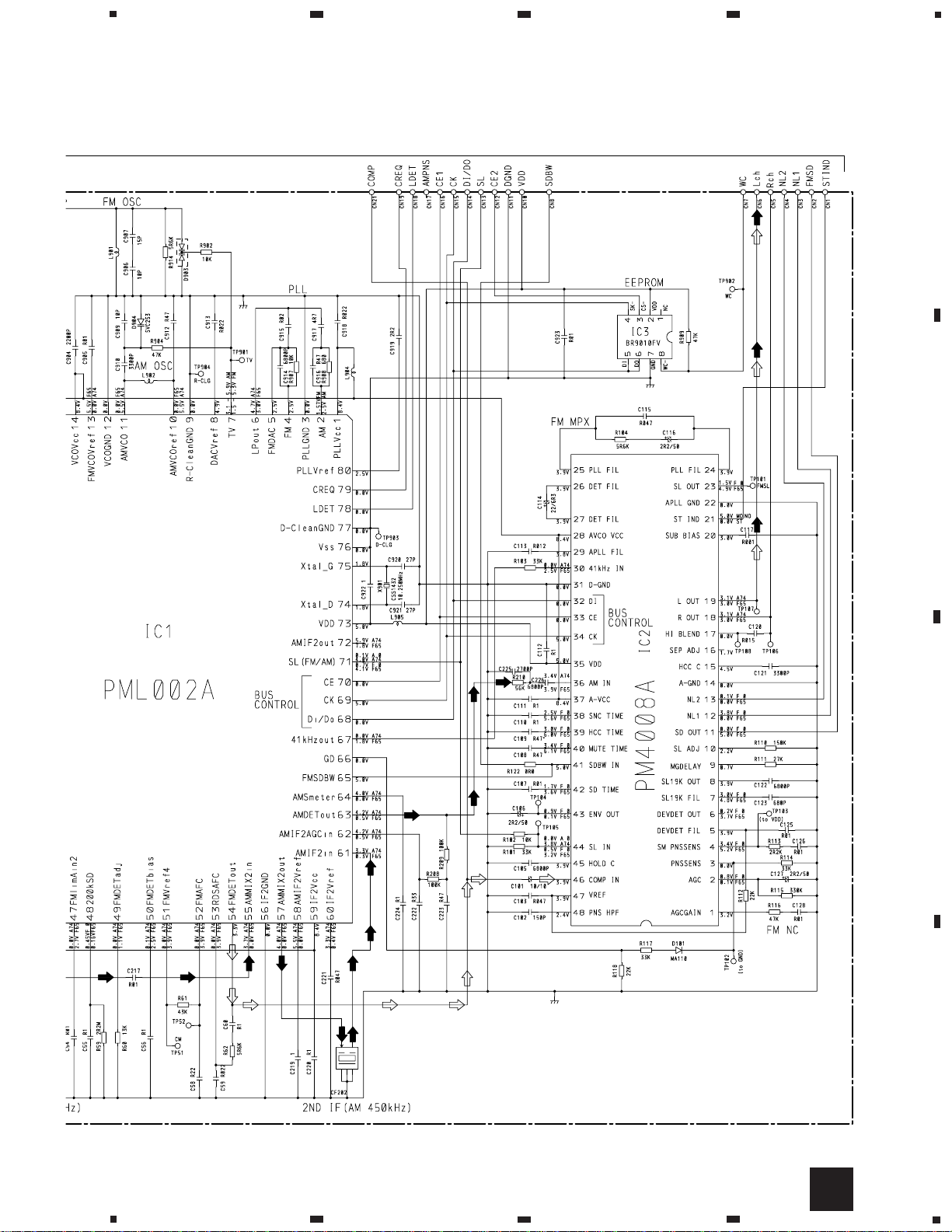
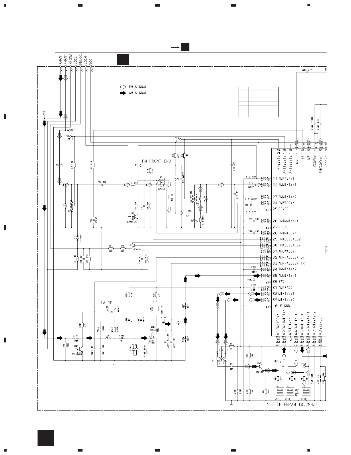
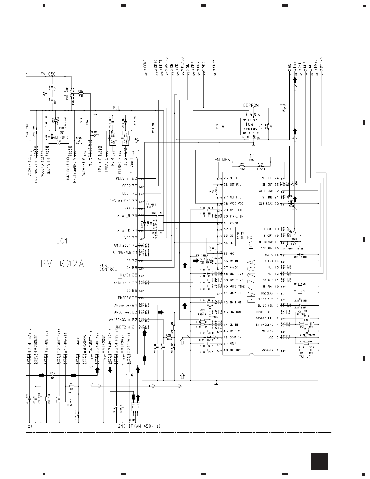
3.3 FM/AM TUNER UNIT(FH-P6600R/EW)
KV1410(23)
KV1410(23)
Mark
None
F0
F65
F125
A0
A74
A125
Band
–
FM
FM
FM
AM
AM
AM
Input Level
–
0dBf
65dBf
125dBf
0dBµ
74dBµ
125dBµ
DAN217U
DAN217U
B
A
FM/AM TUNER UNIT
Page 25
25
FH-P6600R,P6600
5
6
7
8
A
B
C
D
5
6
7
8
B
KV1410(23)
Page 26
26
FH-P6600R,P6600
A
1
234
B
C
D
12
34
B
3.4 FM/AM TUNER UNIT(FH-P6600/ES)
KV1410(23)
Mark
None
F0
F65
F125
A0
A74
A125
Band
–
FM
FM
FM
AM
AM
AM
Input Level
–
0dBf
65dBf
125dBf
0dBµ
74dBµ
125dBµ
DAN217U
B
A
FM/AM TUNER UNIT
Page 27
27
FH-P6600R,P6600
5
6
7
8
A
B
C
D
5
6
7
8
B
KV1410(23)
Page 28
28
FH-P6600R,P6600
A
CN857
A
CN856
A
1
234
B
C
D
12
34
C
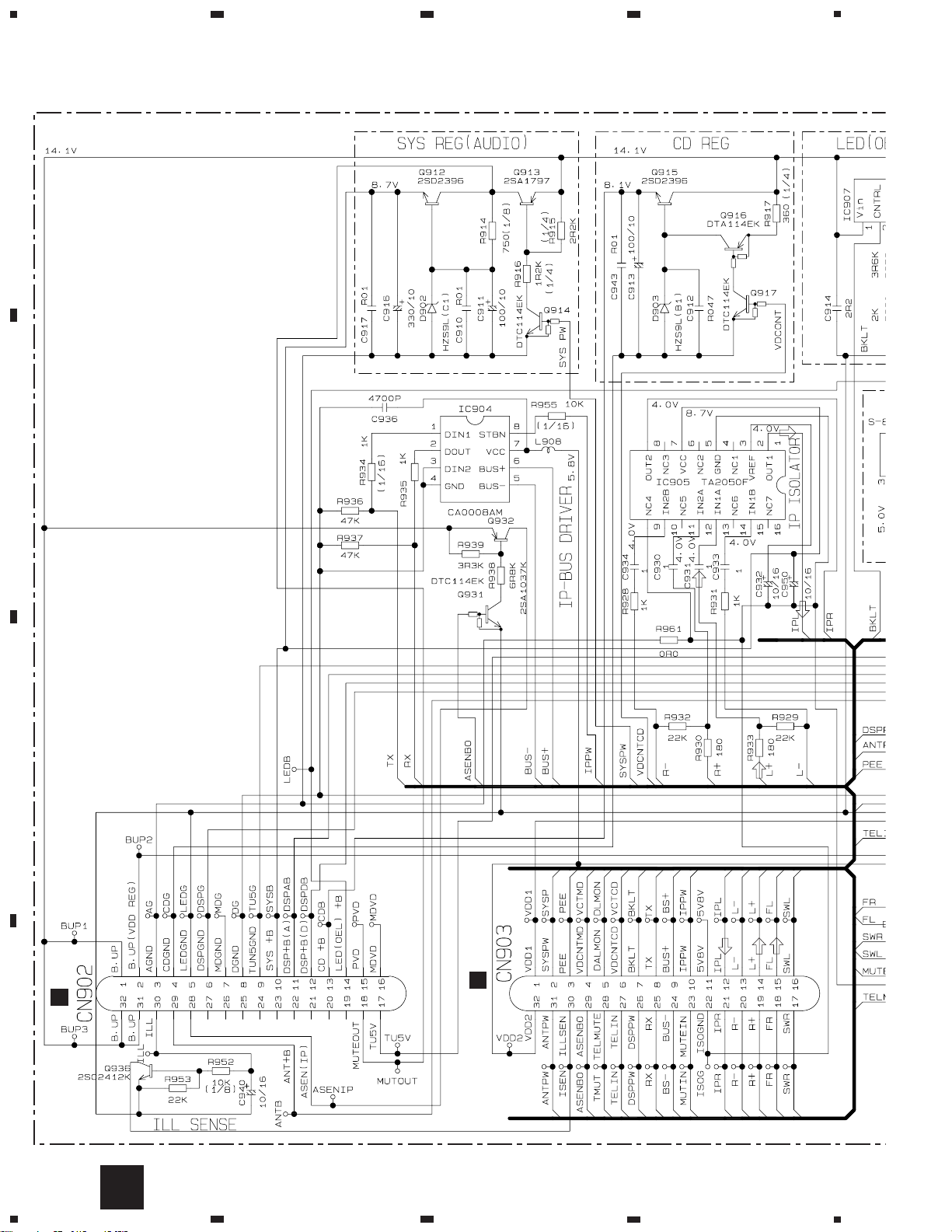
3.5 POWER SUPPLY UNIT
Page 29
29
FH-P6600R,P6600
/ES
RCA CORD
C
POWER SUPPLY UNIT
5
6
7
8
A
B
C
D
5
6
7
8
C
Page 30
30
FH-P6600R,P6600
PTY
D.FUNC
TAPE
CN1102
CN1201
F
E
A
1
234
B
C
D
12
34
D
3.6 FLAP PCB
Page 31

31
FH-P6600R,P6600
5
6
7
8
A
B
C
D
5
6
7
8
D
F
D
FLAP PCB UNIT
FLAP PCB UNIT
Consists of
FLAP PCB
LED PCB
Page 32

32
FH-P6600R,P6600
D
E
CN1902
FLAP PCB UNIT
Consists of
FLAP PCB
LED PCB
LED PCB
A
1
234
B
C
D
12
34
3.7 LED PCB
E
Page 33

33
FH-P6600R,P6600
1
2
3
4
A
B
C
D
1
2
3
4
F
A
CN854
D
CN1901
PANEL PCB UNIT
F
3.8 PANEL PCB UNIT
Page 34

34
FH-P6600R,P6600
A
1
234
B
C
D
12
34
3.9 CD MECHANISM MODULE
H
G H
SPINDLE MOTOR
Q2 CPT230SX-TUQ1 CPT230SX-TU
M3 CXB5829
CARRIAGE MOTOR
M1 CXB5827
M2 CXB5828
LOADING MOTOR
CN101
CN802
CN801
RF-AM
CD DRIVER
5V REGULATOR
CONTROL UNIT(S8TX)
PHOTO UNIT(S8)
G
PICKUP UNIT
(SERVICE)(P8)
Page 35

SWITCHES:
CONTROL UNIT
S801 : HOME SWITCH.....ON-OFF
S802 : CLAMP SWITCH....ON-OFF
The underlined indicates the switch position.
CN601
CN602
CN701
RF-AMP, SERVO, DSP, DAC, LPF
35
FH-P6600R,P6600
5
6
7
8
A
B
C
D
5
6
7
8
A
CN141
G
A
CN251
Page 36

36
FH-P6600R,P6600
1 RFI 0.5V/div. 0.5µs/div.
Normal mode: play
1 CH1: RFI 1V/div.
2 CH2: MIRR 5V/div.
Test mode: Tracking open
0.5ms/div.
1 CH1: RFI 1V/div.
2 CH2: MIRR 5V/div.
Normal mode: The defect part
passes 800µm
0.5ms/div.
3 CH1: FD 0.5V/div.
4 CH2: FO+ 2V/div.
Test mode: No disc, Focus close
0.2s/div.
3 CH1: FD 0.5V/div.
5 CH2: FOK 2V/div.
Normal mode: Focus close
0.2s/div.
6 CH1: FE 0.5V/div.
7 CH2: XSI 2V/div.
Normal mode: Focus close
1ms/div.
REFO
→
8 CH1: TE 0.5V/div.
9 CH2: TD 0.5V/div.
Test mode: 32 tracks jump (FWD)
0.5ms/div.
8 CH1: TE 0.5V/div.
9 CH2: TD 0.5V/div.
Test mode: Single jump (FWD)
0.5ms/div.
8 CH1: TE 0.5V/div.
9 CH2: TD 0.5V/div.
Test mode: 100 tracks jump (FWD)
5ms/div.
6 CH1: FE 0.1V/div.
3 CH2: FD 0.2V/div.
Normal mode: Play
20ms/div.
3 CH1: FD 0.5V/div.
0 CH2: MD 1V/div.
Normal mode: Focus close (12cm)
0.5s/div.
3 CH1: FD 0.5V/div.
0 CH2: MD 1V/div.
Normal mode: Focus close (8cm)
0.5s/div.
REFO
→
REFO
→
REFO
→
REFO
→
REFO
→
REFO
→
GND
→
REFO
→
REFO
→
REFO
→
REFO
→
REFO
→
REFO
→
REFO
→
REFO
→
REFO
→
REFO
→
REFO
→
REFO
→
- Waveforms
Note:1. The encircled numbers denote measuring pointes in the circuit diagram.
2. Reference voltage
REFO:2.5V
REFO
→
REFO
→
REFO
→
REFO
→
Page 37

37
FH-P6600R,P6600
8 CH1: TE 0.2V/div.
9 CH2: TD 0.2V/div.
Normal mode: play
8 CH1: TE 0.5V/div.
! CH2: SD 0.5V/div.
TEST mode: 100 Tracks jump(FWD)
5ms/div.
0 MD 0.5V/div. 0.1s/div.
Normal mode: Play (12cm)
0 MD 1V/div. 10ms/div.
Normal mode:
Long Search (12cm)
@ EFM 1V/div. 5µs/div.
Normal mode: play
8 CH1: TE 1V/div.
# CH2: TEC 1V/div.
Test mode: Focus close
Tracking open
2ms/div.
8 CH1: TE 0.5V/div.
6 CH2: FE 0.5V/div.
Normal mode:
AGC after focus close
0.2s/div.
$ PLCK 2V/div. 0.5µs/div.
Normal mode: play
20ms/div.
% SCKO 2V/div. 1µs/div.
Normal mode: play
^ Dout 2V/div. 10µs/div.
Normal mode: play
& LRCK 2V/div. 20µs/div.
Normal mode: play
* VD 5V/div. 50ms/div.
Normal mode: No disc
GND
→
REFO
→
REFO
→
GND
→
REFO
→
REFO
→
REFO
→
REFO
→
REFO
→
REFO
→
REFO
→
REFO
→
REFO
→
GND
→
REFO
→
GND
→
REFO
→
GND
→
REFO
→
GND
→
REFO
→
Page 38

38
FH-P6600R,P6600
6 CH1: FE 0.2V/div.
3 CH2: FD 0.5V/div.
Normal mode: During AGC
1ms/div.
8 CH1: TE 0.2V/div.
9 CH2: TD 0.5V/div.
Normal mode: During AGC
1 CH1: RFI 1V/div.
⁄ CH2: HOLD 5V/div.
Normal mode: The defect part passes
800µm(B.D)
1ms/div.
0.5ms/div.
3 CH1: FD 0.5V/div.
⁄ CH2: HOLD 5V/div.
Normal mode: The defect part passes
800µm(B.D)
0.5ms/div.
9 CH1: TD 0.1V/div.
⁄ CH2: HOLD 5V/div.
Normal mode: The defect part passes
800µm(B.D)
0.5ms/div.
REFO
→
REFO
→
REFO
→
REFO
→
REFO
→
REFO
→
REFO
→
REFO
→
REFO
→
REFO
→
Page 39

39
FH-P6600R,P6600
Page 40

40
FH-P6600R,P6600
A
1
234
B
C
D
12
34
3.10 CASSETTE MECHANISM MODULE
I
CN111
A
DECK UNIT
MUTE
HA12216F
11
12
13
14
15
16
17
18
19
20
40
39
38
37
36
35
34
33
32
31
30
292827
26
252423
22
21
1
234
5
678
9
10
R256
180
R291
0R0
C271
1/50
R283 0R0
R284 0R0
R282 0R0
C253 390P
C254 390P
C252 390P
C251 330P
R281 0R0
R255
180P
C256
R01
R258
18K
R402
3R3K
R403 910
R322
0R0
R293
0R0
C272
R1
R287
0R0
R285 0R0
HD1
HEAD ASSY
EXA1589
TEST TAPE
NCT-150
(400Hz, 200nWb/m)
RL
RR
FR
FL
C302
R1
VR302
33K(B)
-8.24dBs(300mV)±1dB
Fwd-R
Fwd-L
Rev-R
Rev-L
NFI(L)
RIN(L)
RIP
FIN(L)
GND
GND
FIN(R)
VREF
RIN(R)
NFI(R)
M-OUT(R)
EQOUT(R)
TAI(R)
BIAS
RAI(R)
PBOUT(R)
DET(L)
MUTE
MSGV(R)
MAOUT
MSI
MSDET
MSGV
F/R
120/70
NR
MOUT(L)
EQOUT(L)
TAI(L)
NC
RAI(L)
PBOUT(L)
NC
DET(L)
MSGV(S)
CN252
CN251
DOLBY B NR
IC251
VR301
33K(B)
C310
R1
C309
R1
R321
0R0
VCC
CCP1280
CCP1280
NC
MSOUT
NC
NC
R260
13K
R262
270K
C401
3900P
R401
15K
R276
100K
C402
R33
C404
R01
C403
R022
R288
0R0
R274
0R0
R289
0R0
R273
0R0
R272
0R0
C40
Q271
2SC4116
R292
0R0
R271
18K
C301
R1
R294
0R0
R259
13K
C255
R01
R257
18K
R261
270K
I
Page 41

41
FH-P6600R,P6600
5
6
7
8
A
B
C
D
5
6
7
8
J
I
REEL SENSE
PCB
SWITCHES:
REEL SENSE PCB
S1:LOAD SWITCH..........EJECT-PLAY
S2:MODE SWITCH............ON-OFF
S3:70µs SWITCH...............ON-OFF
The underlined indicates the switch position.
R275
47K
R351 1K
R352 1K
R353 1K
R354 1K
R373 0R0
R355
270K
C352
3900P
R362 300
C351 R22
C353 R01
C354 R01
R374 0R0
C356 R01
C355 R1
D352 1SS355
M1 MOTOR UNIT
(MAIN MOTOR)
EXA1490
S1
LOAD
ESG1007x3
S2
MODE
REEL SENSE
EGN1
EGN1004
M2
MOTOR UNIT
(SUB MOTOR)
EXA1580
RS3
RS2
RS1
SC2
SC1
TAB
MC
CE
VCC2
NC
VCC
MCS
RRS
FRS
RSB
C
TAB
MS2
NC
NC
MM
SM1
RSB
GND
RS
mtl
MCS
load
CN255
CN253
CN256
CN254
MECHANISM
DRIVER
IC351 PA2020A
R375 0R0
S3
70µs
R404
270K
C405
R033
R277
220K
R278
100K
Q271
2SC4116
J
Page 42

42
FH-P6600R,P6600
E
E
E
E
E
E
MOTOR UNIT
G
CN602
C
CORD
CN902
A
1
234
B
C
D
12
34
A
A
AUDIO AMP UNIT
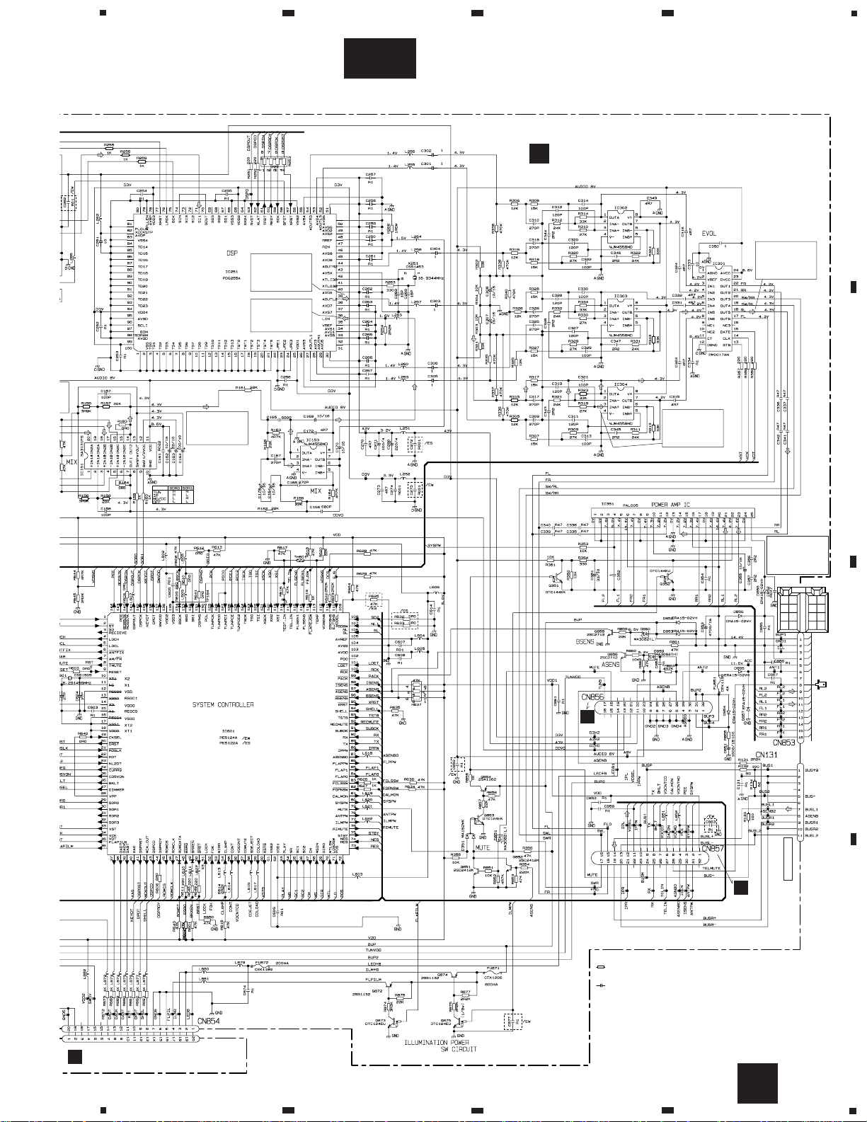
4. PCB CONNECTION DIAGRAM
4.1 AUDIO AMP UNIT
Capacitor
Connector
P.C.Board
Chip Part
SIDE A
SIDE B
NOTE FOR PCB DIAGRAMS
1. The parts mounted on this PCB
include all necessary parts for
several destination.
For further information for
respective destinations, be sure
to check with the schematic
diagram.
2. Viewpoint of PCB diagrams
Page 43

43
FH-P6600R,P6600
E
E
E
E
E
E
E
B
I
CN251
F
CN1101
G
CN701
C
CN903
IP-BUS
ANTENNA
IC,Q
5
6
7
8
A
B
C
D
5
6
7
8
A
SIDE A
FRONT
Page 44

44
FH-P6600R,P6600
E
E
E
E
E
E
IC,Q
FOPN
FEJ
FCLS
A
1
234
B
C
D
12
34
A
A
AUDIO AMP UNIT
Page 45

45
FH-P6600R,P6600
E
E
E
E
E
E
E
5
6
7
8
A
B
C
D
5
6
7
8
A
SIDE B
Page 46

46
FH-P6600R,P6600
A
1
234
B
C
D
12
34
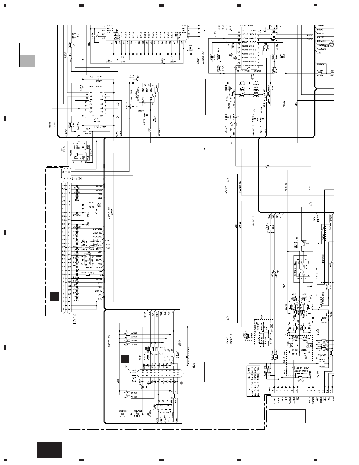
4.2 FM/AM TUNER UNIT
B
SIDE A
FM/AM TUNER UNIT
A
B
Page 47

47
FH-P6600R,P6600
1
2
3
4
A
B
C
D
1
2
3
4
B
FM/AM TUNER UNIT
B
SIDE B
Page 48

48
FH-P6600R,P6600
E
E
E
E
E
E
E
E
CN856
A
A
1
234
B
C
D
12
34
4.3 POWER SUPPLY UNIT
C
POWER SUPPLY UNIT
C
Page 49

49
FH-P6600R,P6600
E
E
E
RCA CORD
CN857
A
IC,Q
5
6
7
8
A
B
C
D
5
6
7
8
C
SIDE A
Page 50

50
FH-P6600R,P6600
E
E
E
E
E
IC,Q
A
1
234
B
C
D
12
34
C
C
POWER SUPPLY UNIT
Page 51

51
FH-P6600R,P6600
E
E
E
E
E
E
E
E
E
5
6
7
8
A
B
C
D
5
6
7
8
C
SIDE B
Page 52

52
FH-P6600R,P6600
A
1
234
B
C
D
12
34
4.4 FLAP PCB
D
D
CN1201
E
CD EJECT
D.FUNC
RESET
ANGLE
SOURCE+
SOURCE-
TA PTY
123 564 DISPLAY
COLOR
VOLUME-
VOLUME+
BAND
DSP
AUDIO
TAPE EJECT
FUNCTION
SIDE A
FLAP PCB
IC,Q
Page 53

53
FH-P6600R,P6600
1
2
3
4
A
B
C
D
1
2
3
4
D
E
E
E
CN1102
F
ADJ POINT
V5
VSS
IC,Q
SIDE B
D
FLAP PCB
IC,Q
Page 54

54
FH-P6600R,P6600
A
1
234
B
C
D
12
34
4.5 LED PCB
D
CN1902
E
LED PCB
E
LED PCB
E
SIDE A SIDE B
Page 55

55
FH-P6600R,P6600
A
CN854
D
CN1901
IL1101
IL1102
1
2
3
4
A
B
C
D
1
2
3
4
F
4.6 PANEL PCB UNIT
F
PANEL PCB UNIT
F
PANEL PCB UNIT
CASSETTE DOOR
DETECTOR
Page 56

F
E
REFO
HOME
CONTROL UNIT(S8TX)
M1 CARRIAGE MOTOR
M2 LOADING MOTOR
M3 SPINDLE MOTOR
PICKUP UNIT(SERVICE)(P8)
CN802
321
PHOTO UNIT(S8)
A
56
FH-P6600R,P6600
A
1
234
B
C
D
12
34
4.7 CD MECHANISM MODULE
CN141
G
H
G
G H
SIDE A
CN251
H
A
Page 57

CLAMP
57
FH-P6600R,P6600
1
2
3
4
A
B
C
D
1
2
3
4
G
SIDE B
CONTROL UNIT(S8TX)
G
Page 58

IC,Q
IC251
Q351
Q352
ADJ
VR302
VR301
IC253
CN252
CN254
CN253
CN255
M1
M2
HEAD ASSY
CN256
21
22
Q271
58
FH-P6600R,P6600
A
1
234
B
C
D
12
34
A
CN111
4.8 CASSETTE MECHANISM MODULE
J
I
SIDE A
SIDE B
CN251
DECK UNIT
I
DECK UNIT
I
Page 59

59
FH-P6600R,P6600
1
2
3
4
A
B
C
D
1
2
3
4
J
J
1
2
3
4
5
6
S3
70µs SW
S1
LOAD SW
S2
MODE SW
CN256
EGN1
REEL SENSE
REEL SENSE PCB
CN253
I
Page 60

60
FH-P6600R,P6600
5. ELECTRICAL PARTS LIST
NOTES:
- Parts whose parts numbers are omitted are subject to being not supplied.
- The part numbers shown below indicate chip components.
Chip Resistor
RS1/_S___J,RS1/__S___J
Chip Capacitor (except for CQS.....)
CKS....., CCS....., CSZS.....
=====Circuit Symbol and No.===Part Name Part No.
--- ------ ------------------------------------------ -------------------------
Unit Number : CWE1500(FH-P6600R/EW)
Unit Name : FM/AM Tuner Unit
MISCELLANEOUS
IC 1 IC PML002A
IC 2 IC PM4008A
IC 3 IC BR9010FV
Q 1 Transistor 2SC4081
Q 2 Transistor DTC124EU
Q 3 FET 3SK263
Q 51 Transistor 2SC4081
Q 201 FET 2SK932
Q 202 Transistor DTC124EU
Q 204 Transistor 2SC4081
D 1 Diode KV1410(23)
D 2 Diode 1SV248
D 4 Diode KV1410(23)
D 6 Diode KV1410(23)
D 101 Diode 1SS355
D 201 Diode DAN217U
D 202 Diode DAN217U
D 903 Diode KV1410(23)
D 904 Diode SVC253
L 1 Coil CTC1155
L 2 Coil CTC1155
L 3 Inductor LCTB100K2125
L 4 Coil CTC1155
L 201 Inductor LCTB330M1608
L 202 Inductor CTF1287
L 203 Inductor LCTA121J3225
L 901 Coil CTC1154
L 902 Inductor LCTA3R3J3225
L 904 Inductor LCTBR47M1608
L 905 Inductor LCTBR47M1608
T 51 Coil CTE1132
CF 51 Ceramic Filter CTF1442
CF 52 Ceramic Filter CTF1442
CF 53 Ceramic Filter CTF1442
CF 202 Ceramic Filter CTF1348
X 901 Crystal Resonator 10.250MHz CSS1432
RESISTORS
R 1 RS1/16S153J
R 2 RS1/16S103J
R 6 RS1/16S103J
R 7 RS1/16S273J
R 8 RS1/16S473J
R 9 RS1/16S223J
R 10 RS1/16S473J
R 11 RS1/16S221J
R 12 RS1/16S103J
R 13 RS1/16S104J
R 16 RS1/16S223J
R 17 RS1/16S221J
R 18 RS1/16S221J
R 19 RS1/16S473J
R 20 RS1/16S470J
R 51 RS1/16S470J
R 52 RS1/16S103J
R 53 RS1/16S103J
R 54 RS1/16S331J
R 55 RS1/16S331J
R 56 RS1/16S560J
R 57 RS1/16S560J
R 58 RS1/16S102J
R 59 RS1/16S225J
R 60 RS1/16S133J
R 61 RS1/16S433J
R 62 RS1/16S562J
R 101 RS1/16S333J
R 102 RS1/16S103J
R 103 RS1/16S333J
R 104 RS1/16S562J
R 110 RS1/16S154J
R 111 RS1/16S273J
R 112 RS1/16S223J
R 113 RS1/16S222J
R 114 RS1/16S333J
R 115 RS1/16S334J
R 116 RS1/16S473J
R 117 RS1/16S333J
R 118 RS1/16S223J
R 122 RS1/16S0R0J
R 202 RS1/16S472J
R 203 RS1/16S225J
R 204 RS1/16S102J
R 205 RS1/16S220J
R 206 RS1/16S471J
R 208 RS1/16S104J
R 209 RS1/16S104J
R 210 RS1/16S563J
R 213 RS1/16S223J
R 251 RS1/16S225J
R 902 RS1/16S103J
R 904 RS1/16S473J
R 907 RS1/16S103J
R 908 RS1/16S681J
R 909 RS1/16S473J
R 914 RS1/16S562J
CAPACITORS
C 1 CCSQCH5R0C50
C 2 CCSRCH5R0C50
C 4 CCSRCJ3R0C50
C 6 CKSQYB105K10
C 8 CKSRYB222K50
=====Circuit Symbol and No.===Part Name Part No.
--- ------ ------------------------------------------ -------------------------
B
Page 61

61
FH-P6600R,P6600
C 10 CCSRCH220J50
C 11 CCSRCH150J50
C 12 CCSRCH8R0D50
C 14 CCSRCJ3R0C50
C 15 CKSRYB103K50
C 16 CKSRYB222K50
C 17 CKSRYB222K50
C 18 CCSRCJ3R0C50
C 19 CKSRYB103K50
C 20 CKSRYB103K50
C 21 CKSRYB103K50
C 24 CKSQYB334K16
C 31 CKSRYB222K50
C 32 CCSRCH470J50
C 35 CKSRYB103K50
C 51 CKSRYB103K50
C 52 CKSRYB473K16
C 53 CCSRCK2R0C50
C 54 CKSRYB103K50
C 55 CKSRYB104K16
C 56 CKSRYB104K16
C 58 CKSQYB224K16
C 59 CKSRYB223K25
C 60 CKSRYB104K16
C 101 CEALNP100M10
C 102 CCSRCH151J50
C 103 CKSRYB473K16
C 105 CKSRYB682K25
C 106 CEAL2R2M50
C 107 CKSRYB103K50
C 108 CKSQYB474K16
C 109 CKSQYB474K16
C 110 CKSRYB104K16
C 111 CKSRYB104K16
C 112 CKSRYB104K16
C 113 CKSRYB123K25
C 114 CEAL220M6R3
C 115 CKSRYB473K16
C 116 CEAL2R2M50
C 117 CKSRYB102K50
C 120 CKSRYB153K25
C 121 CKSRYB332K50
C 122 CKSRYB682K25
C 123 CKSRYB681K50
C 125 CKSRYB103K50
C 126 CKSRYB103K50
C 127 CEAL2R2M50
C 128 CKSRYB103K50
C 201 CCSRCH471J50
C 202 CCSRCH100D50
C 203 CKSRYB104K16
C 204 CKSRYB332K50
C 205 CKSRYB103K50
C 206 CKSRYB104K16
C 207 CKSRYB473K16
C 208 CCSRCH560J50
C 209 CEAL470M6R3
C 210 CKSRYB103K50
C 211 CKSRYB103K50
C 212 CCSRCH101J50
C 215 CKSRYB223K25
C 216 CKSQYB334K16
C 217 CKSRYB103K50
C 219 CKSQYB105K10
C 220 CKSRYB104K16
C 221 CKSRYB473K16
C 222 CKSQYB334K16
C 223 CKSQYB474K16
C 224 CKSRYB104K16
C 225 CKSRYB272K50
C 226 CKSRYB682K25
C 902 CCSRCH270J50
C 904 CKSRYB223K25
C 905 CKSRYB103K50
C 906 CCSRTH100D50
C 907 CCSRTH150J50
C 909 CCSRTH100D50
C 910 CKSRYB332K50
C 912 CKSQYB474K16
C 913 CKSRYB223K25
C 914 CKSRYB682K25
C 915 CKSQYB223K25
C 916 CKSQYB474K16
C 917 CKSYB475K10
C 918 CKSRYB223K25
C 919 CKSQYB225K10
C 920 CCSRCH270J50
C 921 CCSRCH270J50
C 922 CKSYB105K16
C 923 CKSRYB103K50
Unit Number : CWE1501(FH-P6600/ES)
Unit Name : FM/AM Tuner Unit
MISCELLANEOUS
IC 1 IC PML002A
IC 2 IC PM4008A
IC 3 IC BR9010FV
Q 1 Transistor 2SC4081
Q 2 Transistor DTC124EU
Q 3 FET 3SK263
Q 51 Transistor 2SC4081
Q 201 FET 2SK932
Q 202 Transistor DTC124EU
Q 204 Transistor 2SC4081
D 1 Diode KV1410(23)
D 2 Diode 1SV248
D 6 Diode KV1410(23)
D 201 Diode DAN217U
D 202 Diode MA147
D 903 Diode KV1410(23)
D 904 Diode SVC253
L 1 Coil CTC1155
L 3 Inductor LCTB1R5K2125
L 4 Coil CTC1155
L 201 Inductor LCTB330K1608
L 202 Inductor LFEA102J
L 203 Inductor LCTA121J3225
L 901 Coil CTC1154
L 902 Inductor LCTA3R3J3225
L 904 Inductor LCTBR47K1608
L 905 Inductor LCTBR47K1608
T 51 Coil CTE1132
CF 51 Ceramic Filter CTF1442
CF 52 Ceramic Filter CTF1442
CF 53 Ceramic Filter CTF1442
CF 202 Ceramic Filter CTF1476
X 901 Crystal Resonator 10.250MHz CSS1432
=====Circuit Symbol and No.===Part Name Part No.
--- ------ ------------------------------------------ -------------------------
=====Circuit Symbol and No.===Part Name Part No.
--- ------ ------------------------------------------ -------------------------
B
Page 62

62
FH-P6600R,P6600
RESISTORS
R 1 RS1/16S183J
R 2 RS1/16S103J
R 5 RS1/16S0R0J
R 7 RS1/16S273J
R 8 RS1/16S473J
R 9 RS1/16S223J
R 10 RS1/16S473J
R 11 RS1/16S221J
R 12 RS1/16S103J
R 13 RS1/16S104J
R 16 RS1/16S223J
R 17 RS1/16S221J
R 18 RS1/16S221J
R 19 RS1/16S473J
R 20 RS1/16S470J
R 31 RS1/16S0R0J
R 51 RS1/16S470J
R 52 RS1/16S103J
R 53 RS1/16S103J
R 54 RS1/16S331J
R 55 RS1/16S331J
R 56 RS1/16S560J
R 57 RS1/16S560J
R 58 RS1/16S102J
R 59 RS1/16S225J
R 60 RS1/16S133J
R 61 RS1/16S433J
R 101 RS1/16S333J
R 102 RS1/16S103J
R 103 RS1/16S333J
R 104 RS1/16S562J
R 110 RS1/16S154J
R 111 RS1/16S273J
R 113 RS1/16S222J
R 114 RS1/16S333J
R 115 RS1/16S334J
R 116 RS1/16S473J
R 202 RS1/16S472J
R 203 RS1/16S225J
R 204 RS1/16S102J
R 205 RS1/16S220J
R 206 RS1/16S471J
R 208 RS1/16S104J
R 209 RS1/16S104J
R 210 RS1/16S563J
R 213 RS1/16S223J
R 251 RS1/16S225J
R 902 RS1/16S103J
R 904 RS1/16S473J
R 907 RS1/16S103J
R 908 RS1/16S681J
R 909 RS1/16S473J
R 914 RS1/16S562J
CAPACITORS
C 1 CCSQCH4R0C50
C 6 CKSQYB105K10
C 8 CKSRYB222K50
C 10 CCSRCH220J50
C 11 CCSRCH150J50
C 12 CCSRCH8R0D50
C 14 CCSRCJ3R0C50
C 15 CKSRYB103K50
C 16 CKSRYB222K50
C 17 CKSRYB222K50
C 18 CCSRCJ3R0C50
C 19 CKSRYB103K50
C 20 CKSRYB103K50
C 21 CKSRYB103K50
C 24 CKSQYB334K16
C 26 CKSRYB472K50
C 30 CCSRCH220J50
C 32 CCSRCH470J50
C 35 CKSRYB103K50
C 51 CKSRYB103K50
C 52 CKSRYB473K16
C 53 CCSRCK2R0C50
C 54 CKSRYB103K50
C 55 CKSRYB104K16
C 56 CKSRYB104K16
C 58 CKSQYB224K16
C 101 CEALNP100M10
C 102 CCSRCH151J50
C 103 CKSRYB473K16
C 105 CKSRYB682K25
C 106 CEALR68M50
C 107 CKSRYB103K50
C 108 CKSQYB474K16
C 109 CKSQYB474K16
C 110 CKSRYB104K16
C 111 CKSRYB104K16
C 112 CKSRYB104K16
C 113 CKSRYB123K25
C 114 CEAL220M6R3
C 115 CKSRYB473K16
C 116 CEAL2R2M50
C 117 CKSRYB102K50
C 120 CKSRYB183K25
C 121 CKSRYB332K50
C 122 CKSRYB562K25
C 123 CKSRYB681K50
C 125 CKSRYB103K50
C 126 CKSRYB103K50
C 127 CEAL2R2M50
C 128 CKSRYB103K50
C 201 CCSRCH471J50
C 202 CCSRCH100D50
C 203 CKSRYB104K16
C 204 CKSRYB332K50
C 205 CKSRYB103K50
C 206 CKSRYB104K16
C 207 CKSRYB473K16
C 208 CCSRCH560J50
C 209 CEAL470M6R3
C 210 CKSRYB103K50
C 211 CKSRYB103K50
C 212 CCSRCH101J50
C 215 CKSRYB223K25
C 216 CKSQYB334K16
C 217 CKSRYB103K50
C 219 CKSQYB105K10
C 220 CKSRYB104K16
C 221 CKSRYB473K16
C 222 CKSQYB334K16
C 223 CKSQYB474K16
C 224 CKSRYB104K16
C 225 CKSRYB272K50
C 226 CKSRYB682K25
C 902 CCSRCH270J50
C 904 CKSRYB223K25
=====Circuit Symbol and No.===Part Name Part No.
--- ------ ------------------------------------------ -------------------------
=====Circuit Symbol and No.===Part Name Part No.
--- ------ ------------------------------------------ -------------------------
Page 63

63
FH-P6600R,P6600
C 905 CKSRYB103K50
C 906 CCSRTH100D50
C 907 CCSRTH150J50
C 909 CCSRTH100D50
C 910 CKSRYB332K50
C 912 CKSQYB474K16
C 913 CKSRYB223K25
C 914 CKSRYB682K25
C 915 CKSQYB223K25
C 916 CKSQYB474K16
C 917 CKSYB475K10
C 918 CKSRYB223K25
C 919 CKSQYB225K10
C 920 CCSRCH270J50
C 921 CCSRCH270J50
C 922 CKSYB105K16
C 923 CKSRYB103K50
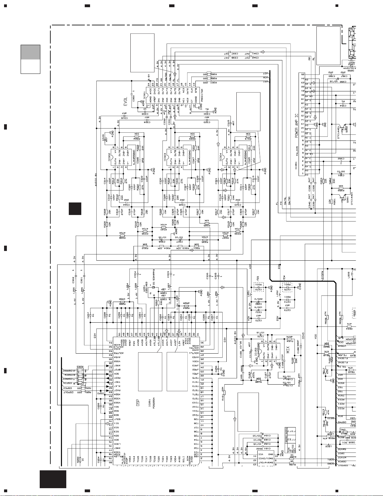
Unit Number : CWM7006(FH-P6600R/EW)
Unit Name : Audio Amp Unit
MISCELLANEOUS
IC 151 IC BA3131FS
IC 153 IC NJM4558MD
IC 251 IC PDG255A
IC 252 IC TC74VHC125FT
IC 253 IC TC7SET08FU
IC 301 IC PM0017AM
IC 302 IC NJM4558MD
IC 303 IC NJM4558MD
IC 304 IC NJM4558MD
IC 351 IC PAL005A
IC 501 IC PM4009A
IC 601 IC PE5124A
IC 602 IC S-80734ANDYI
IC 801 IC TC7W14FU
IC 803 Photo-interrupter GP1S94J
IC 804 Photo-interrupter GP1S94J
IC 805 IC BA6288FS
IC 806 IC BA09SFP
Q 251 Transistor IMH1A
Q 351 Transistor DTC144EK
Q 352 Transistor DTC144EU
Q 401 Transistor 2SC2412K
Q 402 Transistor 2SC2412K
Q 403 Transistor 2SD1757K
Q 404 Transistor 2SD1757K
Q 405 Transistor 2SC2412K
Q 406 Transistor IMH3A
Q 407 Transistor DTA114EK
Q 408 Transistor DTA124EK
Q 501 Transistor DTA124EK
Q 851 Transistor 2SC2412K
Q 852 Transistor 2SC2412K
Q 853 Transistor DTC124EK
Q 854 Transistor 2SA1162
Q 855 Chip Transistor 2SC2712
Q 856 Chip Transistor 2SC2712
Q 871 Transistor 2SA1036K
Q 872 Transistor 2SB1132
Q 873 Transistor DTC124EU
Q 874 Transistor 2SB1132
Q 875 Transistor DTC124EU
D 111 Diode 1SS133
D 351 Diode MA152WK
D 601 Diode MA110
D 801 Diode 1SS133
D 802 Diode 1SS133
D 851 Diode MA3082(L)
D 852 Diode ERA15-02VH
D 853 Diode ERA15-02VH
D 854 Diode ERA15-02VH
D 855 Diode ERA15-02VH
D 856 Diode ERA15-02VH
D 857 Diode ERA15-02VH
D 858 Diode ERA15-02VH
D 859 Diode MA3062(H)
D 860 Diode MA3082(L)
ZNR 451 Surge Protector DSPS-201M-S00B
L 141 Inductor CTF1306
L 142 Inductor CTF1306
L 143 Inductor CTF1306
L 251 Inductor LCTA101J3225
L 252 Inductor CTF1379
L 253 Inductor CTF1305
L 254 Inductor CTF1379
L 255 Inductor CTF1379
L 256 Inductor CTF1379
L 257 Inductor CTF1379
L 258 Inductor CTF1379
L 259 Inductor CTF1379
L 260 Inductor CTF1379
L 261 Inductor CTF1379
L 262 Inductor LCTA471J3225
L 263 Inductor CTF1379
L 264 Inductor CTF1379
L 265 Inductor CTF1379
L 401 Ferri-Inductor LAU4R7K
L 402 Inductor LCTA101J3225
L 403 Inductor CTF1379
L 404 Inductor LCTA4R7J3225
L 405 Inductor CTF1379
L 406 Inductor CTF1379
L 407 Inductor CTF1379
L 408 Inductor CTF1379
L 409 Inductor CTF1379
L 410 Inductor CTF1379
L 411 Inductor CTF1379
L 412 Inductor CTF1379
L 414 Inductor CTF1379
L 501 Inductor LCTA101J3225
L 502 Inductor LCTA101J3225
L 503 Inductor CTF1379
L 504 Inductor CTF1379
L 601 Inductor CTF1379
L 602 Inductor CTF1379
L 603 Inductor LCTB4R7K2125
L 604 Inductor CTF1379
L 605 Inductor CTF1379
L 606 Inductor CTF1379
L 607 Inductor CTF1379
L 608 Inductor CTF1379
L 609 Inductor CTF1379
L 610 Inductor CTF1379
L 611 Inductor CTF1379
L 612 Inductor CTF1379
L 613 Inductor CTF1379
L 614 Inductor CTF1379
L 616 Inductor CTF1379
L 617 Inductor CTF1379
L 618 Inductor CTF1379
L 619 Inductor CTF1379
=====Circuit Symbol and No.===Part Name Part No.
--- ------ ------------------------------------------ -------------------------
=====Circuit Symbol and No.===Part Name Part No.
--- ------ ------------------------------------------ -------------------------
A
Page 64

64
FH-P6600R,P6600
L 620 Inductor CTF1379
L 621 Inductor CTF1379
L 622 Inductor CTF1379
L 851 Inductor CTF1379
L 852 Inductor CTF1379
L 871 Inductor CTF1379
L 872 Inductor CTF1379
L 873 Inductor CTF1379
L 874 Inductor CTF1379
L 875 Inductor CTF1379
L 876 Inductor CTF1379
L 877 Inductor CTF1379
L 878 Inductor CTF1379
L 879 Inductor CTF1379
L 880 Inductor CTF1379
L 881 Inductor CTF1379
L 882 Inductor CTF1379
TH 601 Thermistor CCX1037
X 251 Radiator 16.9344MHz CSS1463
X 501 Crystal Resonator 3.648MHz CSS1447
X 601 Radiator 6.291456MHz CSS1505
S 801 Spring Switch(FEJ) CSN1046
S 802 Spring Switch(FOPN) CSN1046
S 803 Spring Switch(FCLS) CSN1046
FU 851 Micro-Fuse 4A CEK1199
FU 871 Micro-Fuse 800mA CEK1206
FU 872 Micro-Fuse 200mA CEK1189
FM/AM Tuner Unit CWE1500
RESISTORS
R 111 RS1/16S102J
R 112 RS1/16S102J
R 113 RAB4C222J
R 114 RS1/16S473J
R 115 RS1/16S473J
R 117 RS1/16S681J
R 118 RAB4C222J
R 119 RA3C222J
R 120 RS1/16S473J
R 121 RS1/16S473J
R 122 RS1/16S473J
R 123 RS1/16S473J
R 131 RS1/10S222J
R 132 RS1/10S101J
R 133 RS1/10S101J
R 134 RS1/10S620J
R 141 RS1/16S681J
R 142 RA3C102J
R 143 RS1/16S471J
R 144 RS1/16S471J
R 145 RS1/16S471J
R 151 RS1/16S473J
R 152 RS1/16S473J
R 153 RS1/16S473J
R 154 RS1/16S473J
R 155 RS1/16S392J
R 156 RS1/16S392J
R 157 RS1/16S203J
R 158 RS1/16S203J
R 159 RS1/16S102J
R 160 RS1/16S102J
R 161 RS1/16S223J
R 162 RS1/16S223J
R 163 RS1/16S472J
R 164 RS1/16S472J
R 165 RS1/16S223J
R 166 RS1/16S223J
R 173 RS1/16S473J
R 174 RS1/16S473J
R 179 RS1/16S472J
R 180 RS1/16S472J
R 181 RS1/16S123J
R 182 RS1/16S123J
R 183 RS1/16S0R0J
R 184 RS1/16S0R0J
R 251 RS1/16S221J
R 252 RS1/16S221J
R 253 RAB4C221J
R 254 RS1/16S225J
R 255 RS1/16S102J
R 256 RS1/16S102J
R 257 RS1/16S221J
R 259 RS1/16S102J
R 263 RS1/16S331J
R 264 RS1/16S473J
R 265 RS1/16S473J
R 266 RS1/16S155J
R 301 RS1/16S103J
R 302 RS1/16S103J
R 303 RS1/16S103J
R 304 RS1/16S103J
R 305 RN1/16SE1202D
R 306 RN1/16SE1202D
R 307 RS1/16S153J
R 308 RS1/16S153J
R 309 RS1/16S273J
R 310 RS1/16S273J
R 311 RS1/16S243J
R 312 RS1/16S243J
R 313 RS1/16S333J
R 314 RS1/16S333J
R 315 RN1/16SE1202D
R 316 RN1/16SE1202D
R 317 RS1/16S153J
R 318 RS1/16S153J
R 319 RS1/16S273J
R 320 RS1/16S273J
R 321 RS1/16S243J
R 322 RS1/16S243J
R 323 RS1/16S333J
R 324 RS1/16S333J
R 325 RN1/16SE1202D
R 326 RN1/16SE1202D
R 327 RS1/16S153J
R 328 RS1/16S153J
R 329 RS1/16S273J
R 330 RS1/16S273J
R 331 RS1/16S243J
R 332 RS1/16S243J
R 333 RS1/16S333J
R 334 RS1/16S333J
R 335 RS1/16S474J
R 336 RS1/16S474J
R 337 RS1/16S474J
R 338 RS1/16S474J
R 339 RS1/16S474J
R 340 RS1/16S474J
R 351 RS1/10S103J
R 352 RS1/10S103J
R 353 RS1/16S103J
=====Circuit Symbol and No.===Part Name Part No.
--- ------ ------------------------------------------ -------------------------
=====Circuit Symbol and No.===Part Name Part No.
--- ------ ------------------------------------------ -------------------------
Page 65

65
FH-P6600R,P6600
R 354 RS1/10S331J
R 355 RS1/16S103J
R 356 RS1/10S473J
R 357 RS1/16S221J
R 358 RS1/16S221J
R 359 RS1/16S221J
R 401 RS1/16S0R0J
R 402 RS1/16S473J
R 403 RS1/16S473J
R 404 RS1/16S473J
R 405 RS1/16S681J
R 406 RS1/16S103J
R 407 RS1/16S681J
R 408 RS1/16S681J
R 409 RS1/16S681J
R 410 RS1/16S681J
R 411 RS1/16S681J
R 412 RS1/16S681J
R 413 RS1/16S393J
R 414 RS1/16S153J
R 415 RS1/16S162J
R 416 RS1/16S162J
R 417 RS1/16S272J
R 418 RS1/16S272J
R 419 RS1/16S473J
R 420 RS1/16S473J
R 421 RS1/16S472J
R 422 RS1/16S473J
R 425 RS1/16S473J
R 427 RS1/16S224J
R 428 RS1/16S222J
R 429 RS1/16S224J
R 430 RS1/16S224J
R 431 RS1/16S222J
R 432 RS1/16S222J
R 433 RS1/16S222J
R 434 RS1/16S473J
R 435 RS1/16S223J
R 436 RS1/16S223J
R 437 RS1/16S681J
R 438 RS1/16S681J
R 441 RS1/16S102J
R 442 RS1/16S474J
R 447 RS1/16S681J
R 501 RS1/16S102J
R 502 RS1/16S102J
R 503 RS1/16S102J
R 507 RS1/16S0R0J
R 508 RS1/16S0R0J
R 511 RS1/16S102J
R 512 RS1/16S0R0J
R 513 RS1/16S225J
R 518 RS1/16S102J
R 601 RS1/16S473J
R 602 RS1/16S473J
R 603 RS1/16S0R0J
R 604 RS1/8S222J
R 605 RS1/16S0R0J
R 606 RS1/16S0R0J
R 607 RS1/16S472J
R 608 RS1/16S473J
R 609 RS1/16S221J
R 610 RS1/16S0R0J
R 611 RS1/16S221J
R 612 RS1/16S0R0J
R 613 RS1/16S473J
R 614 RS1/16S222J
R 615 RS1/16S473J
R 616 RS1/16S473J
R 617 RS1/16S473J
R 618 RS1/16S473J
R 619 RS1/16S102J
R 620 RN1/16SE2202D
R 622 RS1/16S222J
R 623 RS1/16S222J
R 624 RS1/16S473J
R 626 RS1/16S102J
R 627 RS1/16S102J
R 628 RS1/16S473J
R 629 RS1/16S473J
R 634 RS1/16S473J
R 635 RS1/16S473J
R 636 RS1/16S473J
R 637 RA3C473J
R 638 RS1/16S102J
R 639 RS1/16S124J
R 640 RS1/16S0R0J
R 641 RS1/16S0R0J
R 643 RS1/16S473J
R 644 RS1/16S472J
R 645 RS1/16S222J
R 646 RS1/16S104J
R 647 RS1/16S104J
R 648 RS1/16S221J
R 649 RS1/16S221J
R 650 RS1/16S473J
R 801 RS1/16S221J
R 802 RS1/16S221J
R 803 RS1/16S221J
R 804 RS1/16S473J
R 805 RS1/16S221J
R 806 RS1/16S473J
R 807 RS1/16S102J
R 808 RS1/16S102J
R 851 RS1/16S103J
R 852 RS1/10S472J
R 853 RS1/16S473J
R 854 RS1/16S224J
R 855 RS1/8S101J
R 856 RS1/10S102J
R 857 RS1/10S223J
R 858 RS1/10S473J
R 859 RS1/10S223J
R 860 RS1/10S103J
R 861 RS1/10S473J
R 862 RS1/10S473J
R 863 RS1/10S472J
R 871 RS1/10S223J
R 872 RS1/10S152J
R 873 RS1/16S102J
R 874 RS1/10S332J
R 875 RS1/10S223J
R 876 RS1/8S222J
R 877 RS1/10S222J
R 888 RS1/16S102J
R 889 RS1/16S102J
R 890 RS1/16S102J
R 891 RS1/16S102J
R 892 RS1/16S102J
R 893 RS1/16S102J
=====Circuit Symbol and No.===Part Name Part No.
--- ------ ------------------------------------------ -------------------------
=====Circuit Symbol and No.===Part Name Part No.
--- ------ ------------------------------------------ -------------------------
Page 66

CAPACITORS
C 113 CEJA220M16
C 114 CEJA100M16
C 131 CKSRYB104K16
C 141 CKSYB222K50
C 151 CKSYB105K16
C 152 CKSYB105K16
C 153 CKSYB475K10
C 154 CKSYB475K10
C 155 CKSYB475K10
C 156 CKSYB475K10
C 157 CCSRCH101J50
C 158 CCSRCH101J50
C 161 CKSQYB223K25
C 162 CEV100M16
C 163 CEV220M10
C 164 CEV101M10
C 165 CCSRCH681J50
C 166 CCSRCH681J50
C 167 CCSRCH271J50
C 168 CCSRCH271J50
C 169 CEVNP100M16
C 170 CEVNP100M16
C 172 CKSYB475K10
C 179 CEJA100M16
C 184 CEJA100M16
C 251 CKSYB106K6R3
C 252 CKSRYB104K16
C 253 CKSRYB104K16
C 254 CKSRYB104K16
C 255 CKSRYB104K16
C 256 CKSRYB104K16
C 257 CKSRYB104K16
C 258 CKSRYB104K16
C 259 CKSRYB104K16
C 260 CKSRYB104K16
C 261 CKSRYB104K16
C 262 CKSRYB104K16
C 263 CKSRYB104K16
C 264 CKSRYB104K16
C 265 CKSRYB104K16
C 266 CKSRYB104K16
C 267 CKSRYB104K16
C 268 CCSRCH180J50
C 269 CCSRCH180J50
C 270 CKSYB475K10
C 271 CEV101M4
C 273 CKSYB475K10
C 274 CKSRYB102K50
C 275 CKSRYB102K50
C 276 CCSRCH560J50
C 277 CKSRYB103K25
C 278 CKSRYB103K25
C 280 CEV221M4
C 281 CCSRCH101J50
C 282 CKSRYB103K25
C 301 CKSYB105K16
C 302 CKSYB105K16
C 303 CKSYB105K16
C 304 CKSYB105K16
C 305 CKSYB105K16
C 306 CKSYB105K16
C 307 CEJA100M16
C 308 CEJA100M16
C 309 CCSRCH271J50
C 310 CCSRCH271J50
C 311 CCSRCH121J50
C 312 CCSRCH121J50
C 313 CCSRCH101J50
C 314 CCSRCH101J50
C 315 CKSYB475K10
C 316 CKSYB475K10
C 317 CCSRCH271J50
C 318 CCSRCH271J50
C 319 CCSRCH121J50
C 320 CCSRCH121J50
C 321 CCSRCH101J50
C 322 CCSRCH101J50
C 323 CKSYB475K10
C 324 CKSYB475K10
C 325 CCSRCH271J50
C 326 CCSRCH271J50
C 327 CCSRCH121J50
C 328 CCSRCH121J50
C 329 CCSRCH101J50
C 330 CCSRCH101J50
C 331 CKSYB475K10
C 332 CKSYB475K10
C 333 CKSYB106K6R3
C 334 CKSRYB104K16
C 335 CKSQYB474K16
C 336 CKSQYB474K16
C 337 CKSYB474K16
C 338 CKSYB474K16
C 339 CKSYB474K16
C 340 CKSYB474K16
C 341 CKSQYB474K16
C 342 CKSQYB474K16
C 343 CKSQYB225K10
C 344 CKSQYB225K10
C 345 CKSQYB225K10
C 346 CKSQYB225K10
C 347 CKSQYB225K10
C 348 CKSQYB225K10
C 349 CKSYB475K10
C 350 CKSQYB105K16
C 351 CEJA330M10
C 352 CKSQYB105K16
C 353 4700µF/16V CCH1302
C 354 CKSYB104K50
C 355 CEV100M16
C 356 CKSYB225K16
C 357 CKSYB225K16
C 401 CKSRYB103K25
C 402 CKSRYB182K50
C 404 CKSRYB473K16
C 405 CEJA101M10
C 406 CKSRYB103K25
C 407 CKSRYB123K25
C 408 CKSRYB123K25
C 409 CKSRYB472K50
C 410 CEJA220M10
C 411 CKSRYB223K25
C 412 CKSRYB223K25
C 413 CKSQYB105K16
C 414 CKSQYB105K16
C 415 CKSQYB472K50
C 417 CKSRYB223K25
C 422 CCSRCH101J50
C 424 CCSRCH101J50
C 425 CKSRYB104K16
66
FH-P6600R,P6600
=====Circuit Symbol and No.===Part Name Part No.
--- ------ ------------------------------------------ -------------------------
=====Circuit Symbol and No.===Part Name Part No.
--- ------ ------------------------------------------ -------------------------
Page 67

C 429 CKSRYB104K16
C 430 CCSRCH101J50
C 501 CEV220M6R3
C 503 CCSRCH270J50
C 504 CCSRCH270J50
C 505 CKSRYB104K16
C 506 CCSRCH471J50
C 507 CCSRCH471J50
C 508 CKSRYB104K16
C 509 CEV220M6R3
C 512 CKSRYB104K16
C 513 CKSRYB104K16
C 515 CCSRCH101J50
C 602 CCSRCH270J50
C 603 CKSRYB105K6R3
C 604 CCSRCH270J50
C 605 CKSRYB103K25
C 606 CKSRYB103K25
C 607 CKSRYB103K25
C 608 CKSRYB104K16
C 609 CKSYB225K16
C 612 CKSRYB102K50
C 613 CKSRYB103K25
C 614 CKSRYB104K16
C 801 CKSRYB103K25
C 802 CCSRCH101J50
C 803 CCSRCH101J50
C 804 CEJA220M16
C 805 CKSQYB103K25
C 807 CKSRYB103K25
C 808 CCSRCH101J50
C 851 1000µF/16V CCH1234
C 852 CKSQYB473K50
C 853 CKSRYB104K16
C 854 CKSQYB104K50
C 855 CKSQYB104K16
C 856 CKSQYB104K16
C 857 CKSQYB104K16
C 858 CKSRYB104K16
C 859 CKSRYB104K16
C 861 CKSRYB104K16
C 863 CKSRYB104K16
C 871 CCSQCH221J50
C 872 CCSQCH221J50
C 873 CKSRYB104K16
C 874 CKSRYB104K16
C 877 CKSRYB104K16
Unit Number : CWM7001(FH-P6600/ES)
Unit Name : Audio Amp Unit
MISCELLANEOUS
IC 151 IC BA3131FS
IC 153 IC NJM4558MD
IC 251 IC PDG255A
IC 252 IC TC74VHC125FT
IC 253 IC TC7SET08FU
IC 301 IC PM0017AM
IC 302 IC NJM4558MD
IC 303 IC NJM4558MD
IC 304 IC NJM4558MD
IC 351 IC PAL005A
IC 601 IC PE5122A
IC 602 IC S-80734ANDYI
IC 801 IC TC7W14FU
IC 803 Photo-interrupter GP1S94J
IC 804 Photo-interrupter GP1S94J
IC 805 IC BA6288FS
IC 806 IC BA09SFP
Q 251 Transistor IMH1A
Q 351 Transistor DTC144EK
Q 352 Transistor DTC144EU
Q 402 Transistor 2SC2412K
Q 851 Transistor 2SC2412K
Q 852 Transistor 2SC2412K
Q 853 Transistor DTC124EK
Q 854 Transistor 2SA1162
Q 855 Chip Transistor 2SC2712
Q 856 Chip Transistor 2SC2712
Q 871 Transistor 2SA1036K
Q 872 Transistor 2SB1132
Q 873 Transistor DTC124EU
Q 874 Transistor 2SB1132
Q 875 Transistor DTC124EU
D 111 Diode 1SS133
D 351 Diode MA152WK
D 601 Diode MA110
D 801 Diode 1SS133
D 802 Diode 1SS133
D 851 Diode MA3082(L)
D 852 Diode ERA15-02VH
D 853 Diode ERA15-02VH
D 854 Diode ERA15-02VH
D 855 Diode ERA15-02VH
D 856 Diode ERA15-02VH
D 857 Diode ERA15-02VH
D 858 Diode ERA15-02VH
D 859 Diode MA3062(H)
D 860 Diode MA3082(L)
ZNR 451 Surge Protector DSPS-201M-S00B
L 141 Inductor CTF1306
L 142 Inductor CTF1306
L 143 Inductor CTF1306
L 251 Inductor LCTA101J3225
L 252 Inductor CTF1379
L 253 Inductor CTF1305
L 254 Inductor CTF1379
L 255 Inductor CTF1379
L 256 Inductor CTF1379
L 257 Inductor CTF1379
L 258 Inductor CTF1379
L 259 Inductor CTF1379
L 260 Inductor CTF1379
L 261 Inductor CTF1379
L 262 Inductor LCTA471J3225
L 263 Inductor CTF1379
L 264 Inductor CTF1379
L 265 Inductor CTF1379
L 401 Ferri-Inductor LAU4R7K
L 402 Inductor LCTA101J3225
L 403 Inductor CTF1379
L 404 Inductor LCTA4R7J3225
L 405 Inductor CTF1379
L 406 Inductor CTF1379
L 407 Inductor CTF1379
L 408 Inductor CTF1379
L 409 Inductor CTF1379
L 410 Inductor CTF1379
L 411 Inductor CTF1379
L 412 Inductor CTF1379
L 601 Inductor CTF1379
L 602 Inductor CTF1379
67
FH-P6600R,P6600
=====Circuit Symbol and No.===Part Name Part No.
--- ------ ------------------------------------------ -------------------------
=====Circuit Symbol and No.===Part Name Part No.
--- ------ ------------------------------------------ -------------------------
A
Page 68

L 603 Inductor LCTB4R7K2125
L 604 Inductor CTF1379
L 605 Inductor CTF1379
L 606 Inductor CTF1379
L 607 Inductor CTF1379
L 608 Inductor CTF1379
L 609 Inductor CTF1379
L 610 Inductor CTF1379
L 611 Inductor CTF1379
L 612 Inductor CTF1379
L 613 Inductor CTF1379
L 614 Inductor CTF1379
L 616 Inductor CTF1379
L 617 Inductor CTF1379
L 618 Inductor CTF1379
L 619 Inductor CTF1379
L 620 Inductor CTF1379
L 621 Inductor CTF1379
L 622 Inductor CTF1379
L 851 Inductor CTF1379
L 852 Inductor CTF1379
L 871 Inductor CTF1379
L 872 Inductor CTF1379
L 873 Inductor CTF1379
L 874 Inductor CTF1379
L 875 Inductor CTF1379
L 876 Inductor CTF1379
L 877 Inductor CTF1379
L 878 Inductor CTF1379
L 879 Inductor CTF1379
L 880 Inductor CTF1379
L 881 Inductor CTF1379
L 882 Inductor CTF1379
TH 601 Thermistor CCX1037
X 251 Radiator 16.9344MHz CSS1463
X 601 Radiator 6.291456MHz CSS1505
S 801 Spring Switch(FEJ) CSN1046
S 802 Spring Switch(FOPN) CSN1046
S 803 Spring Switch(FOLS) CSN1046
FU 851 Micro-Fuse 4A CEK1199
FU 871 Micro-Fuse 800mA CEK1206
FU 872 Micro-Fuse 200mA CEK1189
FM/AM Tuner Unit CWE1501
RESISTORS
R 111 RS1/16S102J
R 112 RS1/16S102J
R 113 RAB4C222J
R 114 RS1/16S473J
R 115 RS1/16S473J
R 117 RS1/16S681J
R 118 RAB4C222J
R 119 RA3C222J
R 120 RS1/16S473J
R 121 RS1/16S473J
R 122 RS1/16S473J
R 123 RS1/16S473J
R 131 RS1/10S222J
R 132 RS1/10S101J
R 133 RS1/10S101J
R 134 RS1/10S620J
R 141 RS1/16S681J
R 142 RA3C102J
R 143 RS1/16S471J
R 144 RS1/16S471J
R 145 RS1/16S471J
R 151 RS1/16S473J
R 152 RS1/16S473J
R 153 RS1/16S473J
R 154 RS1/16S473J
R 155 RS1/16S392J
R 156 RS1/16S392J
R 157 RS1/16S203J
R 158 RS1/16S203J
R 159 RS1/16S102J
R 160 RS1/16S102J
R 161 RS1/16S223J
R 162 RS1/16S223J
R 163 RS1/16S472J
R 164 RS1/16S472J
R 165 RS1/16S223J
R 166 RS1/16S223J
R 173 RS1/16S473J
R 174 RS1/16S473J
R 179 RS1/16S472J
R 180 RS1/16S472J
R 181 RS1/16S123J
R 182 RS1/16S123J
R 183 RS1/16S0R0J
R 184 RS1/16S0R0J
R 251 RS1/16S221J
R 252 RS1/16S221J
R 253 RAB4C221J
R 254 RS1/16S225J
R 255 RS1/16S102J
R 256 RS1/16S102J
R 257 RS1/16S221J
R 259 RS1/16S102J
R 263 RS1/16S331J
R 264 RS1/16S473J
R 265 RS1/16S473J
R 266 RS1/16S155J
R 301 RS1/16S103J
R 302 RS1/16S103J
R 303 RS1/16S103J
R 304 RS1/16S103J
R 305 RN1/16SE1202D
R 306 RN1/16SE1202D
R 307 RS1/16S153J
R 308 RS1/16S153J
R 309 RS1/16S273J
R 310 RS1/16S273J
R 311 RS1/16S243J
R 312 RS1/16S243J
R 313 RS1/16S333J
R 314 RS1/16S333J
R 315 RN1/16SE1202D
R 316 RN1/16SE1202D
R 317 RS1/16S153J
R 318 RS1/16S153J
R 319 RS1/16S273J
R 320 RS1/16S273J
R 321 RS1/16S243J
R 322 RS1/16S243J
R 323 RS1/16S333J
R 324 RS1/16S333J
R 325 RN1/16SE1202D
R 326 RN1/16SE1202D
R 327 RS1/16S153J
R 328 RS1/16S153J
=====Circuit Symbol and No.===Part Name Part No.
--- ------ ------------------------------------------ -------------------------
68
FH-P6600R,P6600
=====Circuit Symbol and No.===Part Name Part No.
--- ------ ------------------------------------------ -------------------------
Page 69

69
FH-P6600R,P6600
=====Circuit Symbol and No.===Part Name Part No.
--- ------ ------------------------------------------ -------------------------
=====Circuit Symbol and No.===Part Name Part No.
--- ------ ------------------------------------------ -------------------------
R 329 RS1/16S273J
R 330 RS1/16S273J
R 331 RS1/16S243J
R 332 RS1/16S243J
R 333 RS1/16S333J
R 334 RS1/16S333J
R 335 RS1/16S474J
R 336 RS1/16S474J
R 337 RS1/16S474J
R 338 RS1/16S474J
R 339 RS1/16S474J
R 340 RS1/16S474J
R 351 RS1/10S103J
R 352 RS1/10S103J
R 353 RS1/16S103J
R 354 RS1/10S331J
R 355 RS1/16S103J
R 356 RS1/10S473J
R 357 RS1/16S221J
R 358 RS1/16S221J
R 359 RS1/16S221J
R 401 RS1/16S0R0J
R 403 RS1/16S473J
R 404 RS1/16S473J
R 405 RS1/16S681J
R 406 RS1/16S103J
R 407 RS1/16S681J
R 408 RS1/16S681J
R 409 RS1/16S681J
R 410 RS1/16S681J
R 411 RS1/16S681J
R 413 RS1/16S393J
R 415 RS1/16S272J
R 416 RS1/16S272J
R 417 RS1/16S162J
R 418 RS1/16S162J
R 419 RS1/16S473J
R 420 RS1/16S473J
R 421 RS1/16S472J
R 422 RS1/16S473J
R 423 RS1/16S0R0J
R 424 RS1/16S0R0J
R 425 RS1/16S473J
R 428 RS1/16S222J
R 433 RS1/16S222J
R 440 RS1/16S0R0J
R 601 RS1/16S473J
R 602 RS1/16S473J
R 603 RS1/16S0R0J
R 604 RS1/8S222J
R 605 RS1/16S0R0J
R 606 RS1/16S0R0J
R 607 RS1/16S472J
R 608 RS1/16S473J
R 609 RS1/16S221J
R 610 RS1/16S0R0J
R 611 RS1/16S221J
R 612 RS1/16S0R0J
R 613 RS1/16S473J
R 614 RS1/16S222J
R 615 RS1/16S473J
R 616 RS1/16S473J
R 617 RS1/16S473J
R 618 RS1/16S473J
R 619 RS1/16S102J
R 620 RN1/16SE2202D
R 622 RS1/16S222J
R 623 RS1/16S222J
R 624 RS1/16S473J
R 625 RS1/16S473J
R 626 RS1/16S102J
R 627 RS1/16S102J
R 628 RS1/16S473J
R 629 RS1/16S473J
R 632 RS1/16S0R0J
R 633 RS1/16S0R0J
R 634 RS1/16S473J
R 635 RS1/16S473J
R 636 RS1/16S473J
R 637 RA3C473J
R 638 RS1/16S102J
R 639 RS1/16S124J
R 640 RS1/16S0R0J
R 641 RS1/16S0R0J
R 643 RS1/16S473J
R 644 RS1/16S472J
R 645 RS1/16S222J
R 646 RS1/16S104J
R 647 RS1/16S104J
R 648 RS1/16S221J
R 649 RS1/16S221J
R 650 RS1/16S473J
R 801 RS1/16S221J
R 802 RS1/16S221J
R 803 RS1/16S221J
R 804 RS1/16S473J
R 805 RS1/16S221J
R 806 RS1/16S473J
R 807 RS1/16S102J
R 808 RS1/16S102J
R 851 RS1/16S103J
R 852 RS1/10S472J
R 853 RS1/16S473J
R 854 RS1/16S224J
R 855 RS1/8S101J
R 856 RS1/10S102J
R 857 RS1/10S223J
R 858 RS1/10S473J
R 859 RS1/10S223J
R 860 RS1/10S103J
R 861 RS1/10S473J
R 862 RS1/10S473J
R 863 RS1/10S472J
R 871 RS1/10S223J
R 872 RS1/10S152J
R 873 RS1/16S102J
R 874 RS1/10S332J
R 875 RS1/10S223J
R 876 RS1/8S222J
R 877 RS1/10S222J
R 888 RS1/16S102J
R 889 RS1/16S102J
R 890 RS1/16S102J
R 891 RS1/16S102J
R 892 RS1/16S102J
R 893 RS1/16S102J
CAPACITORS
C 111 CKSRYB104K16
C 113 CEJA220M16
C 114 CEJA100M16
C 131 CKSRYB104K16
C 151 CKSYB105K10
Page 70

C 152 CKSYB105K10
C 153 CKSYB475K10
C 154 CKSYB475K10
C 155 CKSYB475K10
C 156 CKSYB475K10
C 157 CCSRCH101J50
C 158 CCSRCH101J50
C 161 CKSQYB223K25
C 162 CEV100M16
C 163 CEV220M10
C 164 CEV101M10
C 165 CCSRCH681J50
C 166 CCSRCH681J50
C 167 CCSRCH271J50
C 168 CCSRCH271J50
C 169 CEVNP100M16
C 170 CEVNP100M16
C 172 CKSYB475K10
C 179 CEJA100M16
C 184 CEJA100M16
C 251 CKSYB106K6R3
C 252 CKSRYB104K16
C 253 CKSRYB104K16
C 254 CKSRYB104K16
C 255 CKSRYB104K16
C 256 CKSRYB104K16
C 257 CKSRYB104K16
C 258 CKSRYB104K16
C 259 CKSRYB104K16
C 260 CKSRYB104K16
C 261 CKSRYB104K16
C 262 CKSRYB104K16
C 263 CKSRYB104K16
C 264 CKSRYB104K16
C 265 CKSRYB104K16
C 266 CKSRYB104K16
C 267 CKSRYB104K16
C 268 CCSRCH180J50
C 269 CCSRCH180J50
C 270 CKSYB475K10
C 271 CEV101M4
C 272 CKSRYB102K50
C 273 CKSYB475K10
C 274 CKSRYB102K50
C 276 CCSRCH560J50
C 277 CKSRYB103K25
C 278 CKSRYB103K25
C 280 CEV221M4
C 281 CCSRCH101J50
C 301 CKSYB105K16
C 302 CKSYB105K16
C 303 CKSYB105K16
C 304 CKSYB105K16
C 305 CKSYB105K16
C 306 CKSYB105K16
C 307 CEJA100M16
C 308 CEJA100M16
C 309 CCSRCH271J50
C 310 CCSRCH271J50
C 311 CCSRCH121J50
C 312 CCSRCH121J50
C 313 CCSRCH101J50
C 314 CCSRCH101J50
C 315 CKSYB475K10
C 316 CKSYB475K10
C 317 CCSRCH271J50
C 318 CCSRCH271J50
C 319 CCSRCH121J50
C 320 CCSRCH121J50
C 321 CCSRCH101J50
C 322 CCSRCH101J50
C 323 CKSYB475K10
C 324 CKSYB475K10
C 325 CCSRCH271J50
C 326 CCSRCH271J50
C 327 CCSRCH121J50
C 328 CCSRCH121J50
C 329 CCSRCH101J50
C 330 CCSRCH101J50
C 331 CKSYB475K10
C 332 CKSYB475K10
C 333 CKSYB106K6R3
C 334 CKSRYB104K16
C 335 CKSQYB474K16
C 336 CKSQYB474K16
C 337 CKSYB474K16
C 338 CKSYB474K16
C 339 CKSYB474K16
C 340 CKSYB474K16
C 341 CKSQYB474K16
C 342 CKSQYB474K16
C 343 CKSQYB225K10
C 344 CKSQYB225K10
C 345 CKSQYB225K10
C 346 CKSQYB225K10
C 347 CKSQYB225K10
C 348 CKSQYB225K10
C 349 CKSYB475K10
C 350 CKSQYB105K16
C 351 CEJA330M10
C 352 CKSQYB105K16
C 353 4700µF/16V CCH1302
C 354 CKSYB104K50
C 355 CEV100M16
C 356 CKSYB225K16
C 357 CKSYB225K16
C 401 CKSRYB103K25
C 402 CCSRCH101J50
C 404 CKSRYB473K16
C 405 CEJA101M10
C 406 CKSRYB103K25
C 407 CKSRYB183K25
C 408 CKSRYB183K25
C 409 CKSRYB472K50
C 410 CEJA220M10
C 411 CKSRYB223K25
C 412 CKSRYB223K25
C 422 CCSRCH101J50
C 423 CCSRCH101J50
C 429 CKSRYB104K16
C 602 CCSRCH270J50
C 603 CKSRYB105K6R3
C 604 CCSRCH270J50
C 605 CKSRYB103K25
C 606 CKSRYB103K25
C 607 CKSRYB103K25
C 608 CKSRYB104K16
C 609 CKSYB225K16
C 612 CKSRYB102K50
C 613 CKSRYB103K25
70
FH-P6600R,P6600
=====Circuit Symbol and No.===Part Name Part No.
--- ------ ------------------------------------------ -------------------------
=====Circuit Symbol and No.===Part Name Part No.
--- ------ ------------------------------------------ -------------------------
Page 71

C 614 CKSRYB104K16
C 615 CKSRYB222K50
C 801 CKSRYB103K25
C 802 CCSRCH101J50
C 803 CCSRCH101J50
C 804 CEJA220M16
C 805 CKSQYB103K25
C 807 CKSRYB103K25
C 808 CCSRCH101J50
C 851 1000µF/16V CCH1234
C 852 CKSQYB473K50
C 853 CKSRYB104K16
C 854 CKSQYB104K50
C 855 CKSQYB104K16
C 856 CKSQYB104K16
C 857 CKSQYB104K16
C 858 CKSRYB104K16
C 861 CKSRYB104K16
C 871 CCSQCH221J50
C 872 CCSQCH221J50
C 873 CKSRYB104K16
C 874 CKSRYB104K16
Unit Number : CWM7007(FH-P6600R/EW)
: CWM7002(FH-P6600/ES)
Unit Name : Power Supply Unit
MISCELLANEOUS
IC 902 IC S-81250SGUP
IC 903 IC BA033T
IC 904 IC CA0008AM
IC 905 IC TA2050F
IC 906 IC(FH-P6600/ES) TPD1018F
IC 907 IC PQ20RX1S-L
Q 912 Transistor 2SD2396
Q 913 Transistor 2SA1797
Q 914 Transistor DTC114EK
Q 915 Transistor 2SD2396
Q 916 Transistor DTA114EK
Q 917 Transistor DTC114EK
Q 921 Transistor 2SD2396
Q 922 Transistor DTA114EK
Q 923 Transistor DTC124EK
Q 925 Transistor DTC114EK
Q 926 Transistor 2SB1132
Q 927 Transistor DTA114EK
Q 931 Transistor DTC114EK
Q 932 Transistor 2SA1037K
Q 933 Transistor DTC114EU
Q 935 Transistor 2SA1162
Q 936 Transistor 2SC2412K
Q 937 Transistor FMG12
Q 938 Transistor FMG12
D 902 Diode HZS9L(C1)
D 903 Diode HZS9L(B1)
D 905 Diode ERA15-02VH
D 906 Diode HZS6L(C3)
D 908 Diode HZS16L(1)
D 913 Diode MA152WK
D 915 Diode 1SS355
D 917 Diode 1SS355
D 918 Diode 1SS355
D 919 Diode 1SS355
D 920 Diode 1SS355
L 901 Inductor CTF1420
L 902 Inductor CTF1420
L 903 Inductor CTF1420
L 904 Inductor CTF1420
L 905 Inductor CTF1420
L 907 Chip-Inductor LCTA2R2J3225
L 908 Inductor LCTB2R2K2125
L 909 Inductor LCTB2R2K2125
L 910 Inductor LCTA101J3225
BZ 901 Buzzer CPV1012
RESISTORS
R 901 RS1/10S821J
R 902 RS1/10S821J
R 903 RS1/10S821J
R 904 RS1/10S821J
R 909 RS1/10S103J
R 910 RS1/10S103J
R 911 RS1/10S103J
R 912 RS1/10S103J
R 914 RS1/8S751J
R 915 RS1/10S222J
R 916 RS1/4S122J
R 917 RS1/4S361J
R 919 RS1/10S103J
R 920 RS1/8S122J
R 921 RS1/10S102J
R 922 RS1/8S181J
R 923 RS1/4S122J
R 924 RS1/10S561J
R 928 RS1/10S102J
R 929 RS1/10S223J
R 930 RS1/10S181J
R 931 RS1/10S102J
R 932 RS1/10S223J
R 933 RS1/10S181J
R 934 RS1/16S102J
R 935 RS1/10S102J
R 936 RS1/16S473J
R 937 RS1/16S473J
R 938 RS1/10S682J
R 939 RS1/10S332J
R 940 RS1/10S102J
R 941 RS1/10S102J
R 942 (FH-P6600/ES) RS1/10S102J
R 948 RS1/10S183J
R 949 RS1/10S472J
R 950 RS1/10S472J
R 951 RS1/10S102J
R 952 RS1/8S103J
R 953 RS1/10S223J
R 955 RS1/16S103J
R 956 RS1/10S0R0J
R 959 RS1/10S362J
R 960 RS1/10S202J
R 961 RS1/10S0R0J
CAPACITORS
C 903 CKSQYB102K50
C 904 CKSQYB102K50
C 905 CKSQYB102K50
C 906 CKSQYB102K50
C 910 CKSQYB103K25
71
FH-P6600R,P6600
=====Circuit Symbol and No.===Part Name Part No.
--- ------ ------------------------------------------ -------------------------
=====Circuit Symbol and No.===Part Name Part No.
--- ------ ------------------------------------------ -------------------------
C
Page 72

C 911 CEAL101M10
C 912 CKSQYB473K16
C 913 CEAL101M10
C 914 CKSYB225K16
C 915 CEAL100M16
C 916 330µF/10V CCH1181
C 917 CKSQYB103K25
C 918 0.1µF/5.5V CCL1050
C 919 CEAL470M6R3
C 920 CKSQYB103K25
C 921 CKSQYB103K25
C 923 220µF/16V CCH1180
C 924 CCSRCH101J50
C 925 CKSYB106K6R3
C 926 CKSYB225K16
C 930 CKSQYB105K16
C 931 CKSQYB105K16
C 932 CEAL100M16
C 933 CKSQYB105K16
C 934 CKSQYB105K16
C 936 CKSRYB472K50
C 937 CKSRYB103K16
C 938 (FH-P6600/ES) CKSYB225K16
C 940 CEAL100M16
C 943 CKSQYB103K25
C 945 CKSYB475K10
C 946 CKSYB475K10
C 947 CKSYB475K10
C 948 CKSYB475K10
C 949 CKSQYB103K25
C 950 CEAL100M16
C 951 (FH-P6600/ES) CKSQYB473K16
C 953 CKSYB475K10
C 954 CKSQYB225K10
Flap PCB Unit
Consists of
Flap PCB
LED PCB
Unit Number:CWM7009(FH-P6600R/EW)
Unit Name :Flap PCB Unit
MISCELLANEOUS
IC 1901 IC SED1526F0A
IC 1903 IC SBX8035-H
IC 1904 IC M62361FP
IC 1905 IC PE5149A
Q 1919 Transistor DTA114EU
Q 1920 Transistor DTC114EU
Q 1921 Transistor IMX1
Q 1922 Transistor IMX1
Q 1923 Transistor IMX1
Q 1924 Transistor IMX1
Q 1925 Transistor IMX1
Q 1926 Transistor IMX1
Q 1927 Transistor IMX1
Q 1928 Transistor IMX1
Q 1929 Transistor IMX1
Q 1930 Transistor DTA124EU
D 1201 LED NSCM315C
D 1202 LED NSCM315C
D 1203 LED NSCM315C
D 1204 LED NSCM315C
D 1901 LED CL170SRCD
D 1902 LED CL170UBX
D 1903 LED CL170UBX
D 1904 LED CL170SRCD
D 1905 LED CL170SRCD
D 1906 LED CL170SRCD
D 1907 Diode MA111
D 1908 Diode MA111
D 1909 Diode MA111
D 1910 Diode MA111
D 1911 Diode MA111
D 1912 Diode MA111
D 1913 Diode MA111
D 1914 Diode MA111
D 1915 Diode MA111
D 1916 Diode MA111
D 1917 Diode MA111
D 1918 Diode MA111
D 1919 Diode UDZ7R5(B)
D 1922 LED CL170SRCD
D 1923 LED CL170SRCD
L 1901 Coil LCTB150K3216
L 1902 Inductor LCTB2R2K2125
L 1903 Inductor LCTB2R2K2125
X 1901 Ceramic Resonator 4.72MHz CSS1430
S 1901 Push Switch CSG1135
S 1902 Push Switch CSG1135
S 1908 Push Switch CSG1135
S 1909 Push Switch CSG1135
S 1910 Push Switch CSG1135
S 1911 Push Switch CSG1135
S 1912 Push Switch CSG1135
S 1915 Push Switch CSG1135
S 1917 Push Switch CSG1135
S 1926 Push Switch CSG1135
S 1927 Push Switch CSG1135
S 1928 Push Switch CSG1135
S 1929 Push Switch CSG1135
S 1930 Push Switch CSG1135
S 1931 Push Switch CSG1135
S 1932 Push Switch CSG1135
S 1939 Push Switch CSG1111
S 1940 Push Switch CSG1111
S 1941 Push Switch CSG1111
S 1942 Push Switch CSG1111
S 1943 Push Switch CSG1111
S 1944 Push Switch CSG1111
S 1945 Push Switch CSG1111
S 1946 Push Switch CSG1135
S 1947 Switch CSG1041
S 1948 Switch CSG1041
S 1949 Switch CSG1041
S 1950 Switch CSG1041
VR 1901 Semi-fixed 330kΩ(B) CCP1028
EF 1901 EMI Filter CCG1078
LCD1901 LCD CAW1593
RESISTORS
R 1004 RS1/16S102J
R 1005 RAB4C102J
R 1007 RS1/16S473J
R 1008 RS1/16S102J
R 1009 RS1/16S474J
R 1010 RS1/16S102J
R 1011 RS1/16S473J
R 1012 RS1/16S473J
R 1013 RS1/16S102J
R 1014 RS1/16S102J
72
FH-P6600R,P6600
=====Circuit Symbol and No.===Part Name Part No.
--- ------ ------------------------------------------ -------------------------
=====Circuit Symbol and No.===Part Name Part No.
--- ------ ------------------------------------------ -------------------------
D
E
Page 73

R 1015 RAB4C471J
R 1018 RS1/16S102J
R 1019 RS1/16S102J
R 1901 RS1/16S821J
R 1902 RS1/16S821J
R 1903 RS1/16S821J
R 1904 RS1/16S821J
R 1905 RS1/16S821J
R 1906 RS1/16S122J
R 1907 RS1/16S122J
R 1908 RS1/16S122J
R 1909 RS1/16S122J
R 1911 RS1/16S182J
R 1912 RS1/16S182J
R 1913 RS1/16S182J
R 1914 RS1/16S182J
R 1916 RS1/16S622J
R 1917 RS1/16S302J
R 1918 RS1/16S302J
R 1919 RS1/16S302J
R 1920 RS1/16S223J
R 1921 RS1/16S302J
R 1922 RS1/16S622J
R 1923 RS1/16S622J
R 1924 RS1/16S223J
R 1925 RS1/16S622J
R 1926 RS1/16S223J
R 1927 RS1/10S223J
R 1928 RS1/16S472J
R 1929 RS1/16S472J
R 1930 RS1/16S472J
R 1931 RS1/16S472J
R 1932 RS1/16S472J
R 1933 RS1/16S824J
R 1934 RS1/16S684J
R 1935 RS1/16S471J
R 1936 RS1/16S471J
R 1937 RS1/16S471J
R 1938 RS1/16S471J
R 1941 RS1/8S751J
R 1942 RS1/8S471J
R 1943 RS1/8S471J
R 1944 RS1/8S471J
R 1945 RS1/8S471J
R 1946 RS1/8S471J
R 1947 RS1/8S751J
R 1948 RS1/8S471J
R 1949 RS1/8S471J
R 1950 RS1/8S471J
R 1951 RS1/8S471J
R 1952 RS1/8S471J
R 1953 RS1/8S471J
R 1954 RS1/8S471J
R 1955 RS1/8S331J
R 1956 RS1/8S331J
R 1957 RS1/8S331J
R 1958 RS1/8S331J
R 1959 RS1/8S331J
R 1960 RS1/8S331J
R 1961 RS1/8S621J
R 1962 RS1/8S621J
R 1963 RS1/10S241J
R 1964 RS1/10S241J
R 1965 RS1/10S151J
R 1966 RS1/10S241J
R 1967 RS1/10S241J
R 1968 RS1/10S241J
R 1969 RS1/10S151J
R 1970 RS1/10S241J
R 1971 RS1/10S151J
R 1972 RS1/10S241J
R 1973 RS1/10S151J
R 1974 RS1/10S241J
R 1975 RS1/10S101J
R 1976 RS1/10S101J
R 1977 RS1/10S101J
R 1978 RS1/10S101J
R 1979 RS1/10S101J
R 1980 RS1/10S101J
R 1981 RS1/10S101J
R 1982 RS1/10S101J
R 1983 RS1/10S101J
R 1984 RS1/10S101J
R 1985 RS1/10S101J
R 1986 RS1/10S101J
R 1987 RS1/10S104J
R 1988 RS1/10S104J
R 1989 RS1/10S104J
R 1990 RS1/10S222J
R 1991 RS1/10S222J
R 1992 RS1/10S222J
R 1993 RS1/10S102J
R 1994 RS1/10S102J
R 1995 RS1/10S102J
R 1996 RS1/16S102J
R 1997 RS1/16S102J
R 1998 RS1/16S102J
R 1999 RS1/16S101J
R 2004 RS1/16S102J
R 2005 RS1/16S102J
R 2006 RS1/16S102J
R 2007 RS1/16S102J
R 2008 RS1/16S102J
R 2009 RS1/16S102J
R 2010 RS1/16S102J
R 2011 RS1/16S102J
R 2012 RS1/8S471J
R 2013 RS1/8S751J
R 2014 RS1/8S471J
R 2015 RS1/8S751J
CAPACITORS
C 1201 CKSQYB104K16
C 1202 CKSQYB104K16
C 1203 CKSQYB104K16
C 1204 CKSQYB104K16
C 1205 CKSQYB104K16
C 1206 CKSQYB104K16
C 1207 CKSQYB104K16
C 1208 CKSQYB104K16
C 1901 CKSQYB103K25
C 1902 CKSQYB103K25
C 1903 CKSQYB103K25
C 1904 CKSQYB103K25
C 1905 CKSQYB103K25
C 1906 CKSQYB105K16
C 1907 CKSQYB105K16
C 1908 CKSQYB105K16
C 1909 CKSQYB105K16
C 1910 CKSQYB105K16
C 1911 CKSQYB105K16
C 1912 CKSQYB105K16
73
FH-P6600R,P6600
=====Circuit Symbol and No.===Part Name Part No.
--- ------ ------------------------------------------ -------------------------
=====Circuit Symbol and No.===Part Name Part No.
--- ------ ------------------------------------------ -------------------------
Page 74

C 1913 CKSQYB104K16
C 1914 CKSQYB104K16
C 1915 CKSYB225K16
C 1916 CKSQYB104K16
C 1918 CKSQYB104K16
C 1919 CKSQYB104K16
C 1929 CKSQYB104K16
C 1930 CKSYB475K10
C 1931 CKSYB475K10
C 1932 CKSYB475K10
C 1933 CKSYB225K16
C 1951 CKSQYB102K50
C 1952 CKSYB106K6R3
C 1953 CKSQYB103K25
C 1954 CKSQYB103K25
C 1955 CKSRYB102K50
C 1958 CKSRYB102K50
Flap PCB Unit
Consists of
Flap PCB
LED PCB
Unit Number:CWM7004(FH-P6600/ES)
Unit Name :Flap PCB Unit
MISCELLANEOUS
IC 1901 IC SED1526F0A
IC 1903 IC SBX8035-H
IC 1904 IC M62361FP
IC 1905 IC PE5149A
Q 1919 Transistor DTA114EU
Q 1920 Transistor DTC114EU
Q 1921 Transistor IMX1
Q 1922 Transistor IMX1
Q 1923 Transistor IMX1
Q 1924 Transistor IMX1
Q 1925 Transistor IMX1
Q 1926 Transistor IMX1
Q 1927 Transistor IMX1
Q 1928 Transistor IMX1
Q 1929 Transistor IMX1
Q 1930 Transistor DTA124EU
D 1201 LED NSCM315C
D 1202 LED NSCM315C
D 1203 LED NSCM315C
D 1204 LED NSCM315C
D 1901 LED CL170PGCD(AB)
D 1902 LED CL170UBX
D 1903 LED CL170UBX
D 1904 LED CL170PGCD(AB)
D 1905 LED CL170PGCD
D 1906 LED CL170PGCD
D 1907 Diode MA111
D 1908 Diode MA111
D 1909 Diode MA111
D 1910 Diode MA111
D 1911 Diode MA111
D 1912 Diode MA111
D 1913 Diode MA111
D 1914 Diode MA111
D 1915 Diode MA111
D 1916 Diode MA111
D 1917 Diode MA111
D 1918 Diode MA111
D 1919 Diode UDZ7R5(B)
D 1922 LED CL170PGCD(AB)
D 1923 LED CL170PGCD(AB)
L 1901 Coil LCTB150K3216
L 1902 Inductor LCTB2R2K2125
L 1903 Inductor LCTB2R2K2125
X 1901 Ceramic Resonator 4.72MHz CSS1430
S 1901 Push Switch CSG1112
S 1902 Push Switch CSG1112
S 1908 Push Switch CSG1129
S 1909 Push Switch CSG1129
S 1910 Push Switch CSG1129
S 1911 Push Switch CSG1129
S 1912 Push Switch CSG1129
S 1915 Push Switch CSG1129
S 1917 Push Switch CSG1129
S 1926 Push Switch CSG1129
S 1927 Push Switch CSG1129
S 1928 Push Switch CSG1129
S 1929 Push Switch CSG1129
S 1930 Push Switch CSG1129
S 1931 Push Switch CSG1129
S 1932 Push Switch CSG1129
S 1939 Push Switch CSG1111
S 1940 Push Switch CSG1111
S 1941 Push Switch CSG1111
S 1942 Push Switch CSG1111
S 1943 Push Switch CSG1111
S 1944 Push Switch CSG1111
S 1945 Push Switch CSG1111
S 1946 Push Switch CSG1129
S 1947 Switch CSG1041
S 1948 Switch CSG1041
S 1949 Switch CSG1041
S 1950 Switch CSG1041
VR 1901 Semi-fixed 330kΩ(B) CCP1028
EF 1901 EMI Filter CCG1078
LCD1901 LCD CAW1593
RESISTORS
R 1004 RS1/16S102J
R 1005 RAB4C102J
R 1007 RS1/16S473J
R 1008 RS1/16S102J
R 1009 RS1/16S474J
R 1010 RS1/16S102J
R 1011 RS1/16S473J
R 1012 RS1/16S473J
R 1013 RS1/16S102J
R 1014 RS1/16S102J
R 1015 RAB4C471J
R 1018 RS1/16S102J
R 1019 RS1/16S102J
R 1901 RS1/16S821J
R 1902 RS1/16S821J
R 1903 RS1/16S821J
R 1904 RS1/16S821J
R 1905 RS1/16S821J
R 1906 RS1/16S122J
R 1907 RS1/16S122J
R 1908 RS1/16S122J
R 1909 RS1/16S122J
R 1911 RS1/16S182J
R 1912 RS1/16S182J
R 1913 RS1/16S182J
R 1914 RS1/16S182J
R 1916 RS1/16S622J
R 1917 RS1/16S302J
R 1918 RS1/16S302J
R 1919 RS1/16S302J
74
FH-P6600R,P6600
=====Circuit Symbol and No.===Part Name Part No.
--- ------ ------------------------------------------ -------------------------
=====Circuit Symbol and No.===Part Name Part No.
--- ------ ------------------------------------------ -------------------------
D
E
Page 75

R 1920 RS1/16S223J
R 1921 RS1/16S302J
R 1922 RS1/16S622J
R 1923 RS1/16S622J
R 1924 RS1/16S223J
R 1925 RS1/16S622J
R 1926 RS1/16S223J
R 1927 RS1/10S223J
R 1928 RS1/16S472J
R 1929 RS1/16S472J
R 1930 RS1/16S472J
R 1931 RS1/16S472J
R 1932 RS1/16S472J
R 1933 RS1/16S824J
R 1934 RS1/16S684J
R 1935 RS1/16S471J
R 1936 RS1/16S471J
R 1937 RS1/16S471J
R 1938 RS1/16S471J
R 1941 RS1/8S331J
R 1942 RS1/8S471J
R 1943 RS1/8S471J
R 1944 RS1/8S471J
R 1945 RS1/8S471J
R 1946 RS1/8S471J
R 1947 RS1/8S331J
R 1948 RS1/8S471J
R 1949 RS1/8S221J
R 1950 RS1/8S221J
R 1951 RS1/8S221J
R 1952 RS1/8S221J
R 1953 RS1/8S221J
R 1954 RS1/8S221J
R 1955 RS1/8S331J
R 1956 RS1/8S331J
R 1957 RS1/8S331J
R 1958 RS1/8S331J
R 1959 RS1/8S331J
R 1960 RS1/8S331J
R 1961 RS1/8S471J
R 1962 RS1/8S331J
R 1963 RS1/10S241J
R 1964 RS1/10S241J
R 1965 RS1/10S151J
R 1966 RS1/10S241J
R 1967 RS1/10S241J
R 1968 RS1/10S241J
R 1969 RS1/10S151J
R 1970 RS1/10S241J
R 1971 RS1/10S151J
R 1972 RS1/10S241J
R 1973 RS1/10S151J
R 1974 RS1/10S241J
R 1975 RS1/10S101J
R 1976 RS1/10S101J
R 1977 RS1/10S101J
R 1978 RS1/10S101J
R 1979 RS1/10S101J
R 1980 RS1/10S101J
R 1981 RS1/10S101J
R 1982 RS1/10S101J
R 1983 RS1/10S101J
R 1984 RS1/10S101J
R 1985 RS1/10S101J
R 1986 RS1/10S101J
R 1987 RS1/10S104J
R 1988 RS1/10S104J
R 1989 RS1/10S104J
R 1990 RS1/10S222J
R 1991 RS1/10S222J
R 1992 RS1/10S222J
R 1993 RS1/10S102J
R 1994 RS1/10S102J
R 1995 RS1/10S102J
R 1996 RS1/16S102J
R 1997 RS1/16S102J
R 1998 RS1/16S102J
R 1999 RS1/16S101J
R 2004 RS1/16S102J
R 2005 RS1/16S102J
R 2006 RS1/16S102J
R 2007 RS1/16S102J
R 2008 RS1/16S102J
R 2009 RS1/16S102J
R 2010 RS1/16S102J
R 2011 RS1/16S102J
R 2012 RS1/8S471J
R 2013 RS1/8S331J
R 2014 RS1/8S471J
R 2015 RS1/8S331J
CAPACITORS
C 1201 CKSQYB104K16
C 1202 CKSQYB104K16
C 1203 CKSQYB104K16
C 1204 CKSQYB104K16
C 1205 CKSQYB104K16
C 1206 CKSQYB104K16
C 1207 CKSQYB104K16
C 1208 CKSQYB104K16
C 1901 CKSQYB103K25
C 1902 CKSQYB103K25
C 1903 CKSQYB103K25
C 1904 CKSQYB103K25
C 1905 CKSQYB103K25
C 1906 CKSQYB105K16
C 1907 CKSQYB105K16
C 1908 CKSQYB105K16
C 1909 CKSQYB105K16
C 1910 CKSQYB105K16
C 1911 CKSQYB105K16
C 1912 CKSQYB105K16
C 1913 CKSQYB104K16
C 1914 CKSQYB104K16
C 1915 CKSYB225K16
C 1916 CKSQYB104K16
C 1918 CKSQYB104K16
C 1919 CKSQYB104K16
C 1929 CKSQYB104K16
C 1930 CKSYB475K10
C 1931 CKSYB475K10
C 1932 CKSYB475K10
C 1933 CKSYB225K16
C 1951 CKSQYB102K50
C 1952 CKSYB106K6R3
C 1953 CKSQYB103K25
C 1954 CKSQYB103K25
C 1955 CKSRYB102K50
C 1958 CKSRYB102K50
75
FH-P6600R,P6600
=====Circuit Symbol and No.===Part Name Part No.
--- ------ ------------------------------------------ -------------------------
=====Circuit Symbol and No.===Part Name Part No.
--- ------ ------------------------------------------ -------------------------
Page 76

Unit Number : CWM7008(FH-P6600R/EW)
Unit Name : Panel PCB Unit
MISCELLANEOUS
D 1101 LED CL170SRCD
D 1102 LED CL170SRCD
D 1103 LED CL170SRCD
D 1105 LED CL170SRCD
S 1101 Spring Switch CSN1051
IL 1101 Lamp 40mA 14V CEL1648
IL 1102 Lamp 40mA 14V CEL1648
RESISTORS
R 1101 RS1/8S621J
R 1102 RS1/8S391J
R 1103 RS1/8S621J
R 1104 RS1/8S391J
CAPACITORS
C 1101 CKSQYB103K25
Unit Number : CWM7003(FH-P6600/ES)
Unit Name : Panel PCB Unit
MISCELLANEOUS
D 1101 LED CL170FGCD
D 1102 LED CL170FGCD
D 1103 LED CL170FGCD
D 1105 LED CL170FGCD
S 1101 Spring Switch CSN1051
IL 1101 Lamp 40mA 14V CEL1647
IL 1102 Lamp 40mA 14V CEL1647
RESISTORS
R 1101 RS1/8S331J
R 1102 RS1/8S391J
R 1103 RS1/8S331J
R 1104 RS1/8S391J
CAPACITORS
C 1101 CKSQYB103K25
Unit Number : EWY1031
Unit Name : Deck Unit
MISCELLANEOUS
IC 251 IC HA12216F
IC 351 IC PA2020A
Q 271 Transistor 2SC4116
D 352 Diode 1SS355
VR 301 Semi-fixed 33kΩ(B) CCP1280
VR 302 Semi-fixed 33kΩ(B) CCP1280
RESISTORS
R 255 RS1/16S181J
R 256 RS1/16S181J
R 257 RS1/16S183J
R 258 RS1/16S183J
R 259 RS1/16S133J
R 260 RS1/16S133J
R 261 RS1/16S274J
R 262 RS1/16S274J
R 271 RS1/16S183J
R 272 RS1/8S0R0J
R 273 RS1/8S0R0J
R 274 RS1/8S0R0J
R 275 RS1/16S473J
R 276 RS1/16S104J
R 277 RS1/16S224J
R 278 RS1/16S104J
R 281 RS1/8S0R0J
R 282 RS1/8S0R0J
R 283 RS1/8S0R0J
R 284 RS1/8S0R0J
R 285 RS1/16S0R0J
R 287 RS1/16S0R0J
R 288 RS1/16S0R0J
R 289 RS1/16S0R0J
R 291 RS1/8S0R0J
R 292 RS1/10S0R0J
R 293 RS1/10S0R0J
R 294 RS1/10S0R0J
R 321 RS1/8S0R0J
R 322 RS1/8S0R0J
R 351 RS1/16S102J
R 352 RS1/16S102J
R 353 RS1/16S102J
R 354 RS1/16S102J
R 355 RS1/10S274J
R 362 RS1/8S301J
R 373 RS1/8S0R0J
R 374 RS1/8S0R0J
R 375 RS1/8S0R0J
R 401 RS1/16S153J
R 402 RS1/16S332J
R 403 RS1/16S911J
R 404 RS1/16S274J
CAPACITORS
C 251 CKSRYB391K50
C 252 CKSRYB391K50
C 253 CKSRYB391K50
C 254 CKSRYB391K50
C 255 CKSRYB103K50
C 256 CKSRYB103K50
C 271 CEJA1R0M50
C 272 CKSQYB104K16
C 301 CKSQYB104K16
C 302 CKSQYB104K16
C 309 CKSQYB104K16
C 310 CKSQYB104K16
C 351 CKSYB224K25
C 352 CKSRYB392K50
C 353 CKSRYB103K50
C 354 CKSRYB103K50
C 355 CKSYB104K50
C 356 CKSRYB103K50
C 401 CKSRYB392K50
C 402 CKSQYB334K16
C 403 CKSRYB223K25
C 404 CKSRYB103K50
C 405 CKSRYB333K16
Unit Number :
Unit Name : Reel Sense PCB
MISCELLANEOUS
S 1 Switch(LOAD) ESG1007
S 2 Switch(MODE) ESG1007
S 3 Switch(70µs) ESG1007
EGN 1 Photo-reflector EGN1004
76
FH-P6600R,P6600
J
I
F
=====Circuit Symbol and No.===Part Name Part No.
--- ------ ------------------------------------------ -------------------------
=====Circuit Symbol and No.===Part Name Part No.
--- ------ ------------------------------------------ -------------------------
F
Page 77

Unit Number : CWX2434
Unit Name : Control Unit(S8TX)
MISCELLANEOUS
IC 201 IC UPD63711GC
IC 301 IC BA5985FM
IC 701 IC BA05SFP
Q 101 Transistor 2SB1132
D 801 Chip LED CL200IRX
D 802 Chip LED CL200IRX
S 801 Spring Switch(HOME) CSN1051
S 802 Spring Switch(CLAMP) CSN1052
RESISTORS
R 101 RS1/8S120J
R 102 RS1/8S100J
R 103 RS1/16S222J
R 201 RS1/16S104J
R 202 RS1/16S103J
R 203 RS1/16S393J
R 204 RS1/16S103J
R 205 RS1/16S103J
R 206 RS1/16S182J
R 207 RS1/16S123J
R 211 RS1/16S0R0J
R 212 RS1/16S272J
R 302 RS1/16S153J
R 303 RS1/16S103J
R 501 RS1/16S102J
R 502 RA4C681J
R 503 RS1/16S221J
R 504 RS1/16S221J
R 505 RS1/16S221J
R 801 RS1/8S751J
R 803 RS1/8S751J
R 901 RS1/16S681J
R 903 RS1/16S0R0J
R 904 RS1/16S681J
R 905 RS1/16S681J
CAPACITORS
C 101 CKSRYB102K50
C 102 CKSRYB104K16
C 103 CEV101M6R3
C 104 CEV470M6R3
C 105 CKSQYB334K16
C 106 CKSQYB334K16
C 107 CKSQYB334K16
C 201 CKSRYB104K16
C 202 CKSRYB471K50
C 203 CKSRYB104K16
C 205 CEV101M6R3
C 206 CKSRYB104K16
C 207 CKSRYB104K16
C 208 CKSRYB104K16
C 209 CKSRYB104K16
C 210 CKSRYB332K50
C 211 CKSRYB104K16
C 212 CKSRYB104K16
C 213 CKSRYB392K50
C 214 CKSRYB104K16
C 215 CKSRYB104K16
C 216 CCSRCJ3R0C50
C 217 CCSRCH270J50
C 218 CKSRYB104K16
C 219 CCSRCH181J50
C 220 CCSRCH510J50
C 221 CKSRYB682K25
C 223 CCSRCH221J50
C 301 CEV101M10
C 702 10µF/10V CCH1349
C 703 CKSQYB334K16
Unit Number :
Unit Name : Photo Unit(S8)
Q 1 Photo-transistor CPT230SX-TU
Q 2 Photo-transistor CPT230SX-TU
Miscellaneous Parts List
Pickup Unit(Service)(P8) CXX1285
M 1 Motor Unit(CARRIAGE) CXB5827
M 2 Motor Unit(LOADING) CXB5828
M 3 Motor Unit(SPINDLE) CXB5829
M 1 Motor Unit(MAIN) EXA1490
M 2 Motor Unit(SUB) EXA1580
HD 1 Head Assy EXA1589
77
FH-P6600R,P6600
G
H
=====Circuit Symbol and No.===Part Name Part No.
--- ------ ------------------------------------------ -------------------------
=====Circuit Symbol and No.===Part Name Part No.
--- ------ ------------------------------------------ -------------------------
Page 78

78
FH-P6600R,P6600
6. ADJUSTMENT
6.1 GRILLE AND CASSETTE SECTION
- Connection Diagram
CONTRAST VOLTAGE ADJUSTMENT(GRILLE)
No. Adjustment Point Adjustment Method
(Switch Position)
1 VR1901 Oscilloscope : -2.4V±0.1V
VR302
mV
Meter(2)
VR301
L-CH
R-CH
Pin2
Pin3
CN251
DECK UNIT
Extention Cord GGD1121
DOLBY B NR ADJUSTMENT(CASSETTE)
No. Test Tape Adjustment Point Adjustment Method
(Switch Position)
1 NCT-150 VR301(Lch),VR302(Rch) mV Meter : –8.24dBm(300mV)±1dB
(400Hz,200nwb/m) (DOLBY NR Switch : OFF)
Oscilloscope
Page 79

79
FH-P6600R,P6600
1) Precautions
• This unit uses a single power supply (+5V) for the
regulator. The signal reference potential, therefore, is
connected to REFO(approx. 2.5V) instead of GND.
If REFO and GND are connected to each other by
mistake during adjustments, not only will it be
impossible to measure the potential correctly, but the
servo will malfunction and a severe shock will be
applied to the pick-up. To avoid this, take special note
of the following.
Do not connect the negative probe of the measuring
equipment to REFO and GND together. It is especially
important not to connect the channel 1 negative
probe of the oscilloscope to REFO with the channel 2
negative probe connected to GND.
Since the frame of the measuring instrument is
usually at the same potential as the negative probe,
change the frame of the measuring instrument to
floating status.
If by accident REFO comes in contact with GND,
immediately switch the regulator or power OFF.
• Always make sure the regulator is OFF when
connecting and disconnecting the various filters and
wiring required for measurements.
• Before proceeding to further adjustments and
measurements after switching regulator ON, let the
player run for about one minute to allow the circuits
to stabilize.
• Since the protective systems in the unit's software are
rendered inoperative in test mode, be very careful to
avoid mechanical and /or electrical shocks to the
system when making adjustment.
• Disc detection during loading and eject operations is
performed by means of a photo transistor in this
unit.Consequently, if the inside of the unit is exposed
to a strong light source when the outer casing is
removed for repairs or adjustment, the following
malfunctions may occur.
*During PLAY, even if the eject button is
pressed,the disc will not be ejected and the unit
will remain in the PLAY mode.
*The unit will not load a disc.
When the unit malfunctions this way, either reposition the light source, move the unit or cover the
photo transistor.
2) Test Mode
This mode is used for adjusting the CD mechanism
module of the device.
• Test mode starting procedure
Reset while pressing the 4 and 6 keys together.
• Test mode cancellation
Switch ACC, back-up OFF.
• After pressing the EJECT key, do not press any other
key until the disk is completely ejected.
• If the ] or [ key is pressed while focus search is in
progress, immediately turn the power off (otherwise
the actuator may be damaged due to adhesion of the
lenses).
• Jump operation of TRs other than 100TR continues
after releasing the key. CRG move and 100TR jump
operations are brought into the “Tracking close”
status when the key is released.
• Powering Off/On resets the jump mode to “Single TR
(91)”, the RF AMP gain setting to 0 dB, and the
automatic adjustment value to the initial value.
6.2 CD ADJUSTMENT
Page 80

80
FH-P6600R,P6600
- Flow Chart
Focus Close*2S Curve Check
01 01 0100 00 00
(99 99 99)
Display
TYP
4
3
Acc on
SOURCE
New test mode
[
BAND
BAND
BAND
BAND
BAND
3
*2
*1
+6dB +12dB
*4
*5
6
6
6
6
1
2
1
2]
][
06 06 06 12 12 12
Sourse CD
Single TR 32TRK
92(82)
CRG Move
94(84)
100TRK
93(83)
Focus Mode
Select
Focus Close/
S Curve Check
CRG-
Auto Adjustment
Display Select
<Tracking Servo Close> CRG+
RF AGC Coefficient Display/
Rough Servo and RF AGC
Tracking
Open
Display
Tracking
Open
T. Close and
Fit Servo
*3 F.Offset Display RF.Offset Display F.Cansel Display
*7
Single TR/32TR/100TR
Voltage of CRG Motor = 2 [V]
(F,T.AGC Gain = (Present Value/Initial Value) x 20)
*6
][
1
3
Display
2
3
Display
or
8x 8x 8x
TRK SECMIN
9x 9x 9x
TRK SECMIN
or
CRG-CRG+
T.Balance
Adjustment
*7
F, T, RF AGC/
F.Bias Display Select
F, T AGC and
RF AGC
CRG Move, 100TR Jump Only
TRK, MIN, SEC F.AGC Gain
RF AGC Gain
T.AGC Gain
*8
Power ON
(Adjustment for T.Offset)
*5
*4 *4
*6
CRG/TR Jump NO.
Select
CRG+/TR Jump+
CRG-/TR Jump-
Power OFF
Display
Display
Display
T.Close and
F,T AGC and
RF AGC and
Fit Servo
Display
Power ON
(Not adjustment for T.Offset)
Display
Display
2
RF AMP Gain Select
2
Power OFF
Power OFF
Power OFF
8x 8x 8x
TRK SECMIN
9x 9x 9x
TRK SECMIN
8x 8x 8x
TRK SECMIN
9x 9x 9x
TRK SECMIN
or
8x 8x 8x
TRK SECMIN
9x 9x 9x
TRK SECMIN
or
00 00 00
TRK SECMIN
99 99 99
TRK SECMIN
or
00 00 00
TRK SECMIN
99 99 99
TRK SECMIN
or
00 00 00
TRK SECMIN
99 99 99
TRK SECMIN
or
91 91 91
TRK SECMIN
0x 0x 0x
TRK SECMIN
00 00 00
TRK SECMIN
99 99 99
TRK SECMIN
GG GG GG
TRK SECMIN
Test Mode In
*1
*8 *3*8
F.Cancel Value = {Top Rank 8bit of Set Value (7F [H] to 80 [H] ) + 128} / 4
= 63 [D] to (32 [D] ) to 00 [D]
9x(8x):91(81)
6
Page 81

81
FH-P6600R,P6600
• Note :
The grating angle of the PU unit cannot be adjusted after the PU unit is changed. The PU unit in the CD
mechanism module is adjusted on the production line to match the CD mechanism module and is thus the best
adjusted PU unit for the CD mechanism module. Changing the PU unit is thus best considered as a last resort.
However, if the PU unit must be changed, the grating should be checked using the procedure below.
• Purpose :
To check that the grating is within an acceptable range when the PU unit is changed.
• Symptoms of Mal-adjustment :
If the grating is off by a large amount symptoms such as being unable to close tracking, being unable to perform
track search operations, or taking a long time for track searching.
• Method :
• Measuring Equipment • Oscilloscope, Two L.P.F.
• Measuring Points • E, F, REFO
• Disc • ABEX TCD-784
• Mode • TEST MODE
• Checking Procedure
1. In test mode, load the disc and switch the 5V regulator on.
2. Using the ] and [ buttons, move the PU unit to the innermost track.
3. Press key 3 to close focus, the display should read "91". Press key 2 to implement the tracking balance
adjustment the display should now read "81". Press key 3 2 times. The display will change, returning to "81" on
the fourth press.
4. As shown in the diagram above, monitor the LPF outputs using the oscilloscope and check that the phase
difference is within 75° . Refer to the photographs supplied to determine the phase angle.
5. If the phase difference is determined to be greater than 75° try changing the PU unit to see if there is any
improvement. If, after trying this a number of times, the grating angle does not become less than 75° then the
mechanism should be judged to be at fault.
• Note
Because of eccentricity in the disc and a slight misalignment of the clamping center the grating waveform may be
seen to "wobble" ( the phase difference changes as the disc rotates). The angle specified above indicates the
average angle.
• Hint
Reloading the disc changes the clamp position and may decrease the "wobble".
F
REFO
E
100kΩ
390pF
100kΩ
390pF
E
REFO
F
REFO
L.P.F.
L.P.F.
CONTROL UNIT
Xch Ych
Oscilloscope
6.3 CHECKING THE GRATING AFTER CHANGING THE PICKUP UNIT
Page 82

82
FH-P6600R,P6600
Grating waveform
Ech → Xch 20mV/div, AC
Fch → Ych 20mV/div, AC
45°
0°
75°
60°
30°
90°
Page 83

83
FH-P6600R,P6600
7. GENERAL INFORMATION
7.1 DIAGNOSIS
7.1.1 TEST MODE
- Error Messages
If a CD is not operative or stopped during operation due to an error, the error mode is turned on and cause(s) of the
error is indicated with a corresponding number. This arrangement is intended at reducing nonsense calls from the
users and also for facilitating trouble analysis and repair work in servicing.
(1) Basic Indication Method
1) When SERRORM is selected for the CSMOD (CD mode area for the system), error codes are written to DMIN
(minutes display area) and DSEC (seconds display area). The same data is written to DMIN and DSEC. DTNO
remains in blank as before.
2) Main unit display examples
Depending on display capability of LCD used, display will vary as shown below. xx contains the error number.
8-digit display 6-digit display 4-digit display
ERROR–xx ERR–xx E–xx
OR
Err–xx
(2) Error Code List
Code Class Displayed error code Description of the code and potential cause(s)
10 Electricity Carriage Home NG CRG can't be moved to inner diameter.
CRG can't be moved from inner diameter.
→ Failure on home switch or CRG move mechanism.
11 Electricity Focus Servo NG Focusing not available.
→ Stains on rear side of disc or excessive vibrations on REWRITABLE.
12 Electricity Spindle Lock NG Spindle not locked. Sub-code is strange (not readable).
→ Failure on spindle, stains or damages on disc, or excessive vibrations.
Subcode NG A disc not containing CD-R data is found. Turned over disc are found,
though rarely.
→ Failure on home switch or CRG move mechanism.
RF AMP NG An appropriate RF AMP gain can't be determined.
→ CD signal error.
17 Electricity Setup NG APC protection doesn't work. Focus can be easily lost.
→ Damages or stains on disc, or excessive vibrations.
30 Electricity Search Time Out Failed to reach target address.
→ CRG tracking error or damages on disc.
A0 System Power Supply NG Power (VD) is ground faulted.
→ Failure on SW transistor or power supply (failure on connector).
Remarks: Mechanical errors are not displayed (because a CD is turned off in these errors).
Unreadable TOC does not constitute an error. An intended operation continues in this case.
A newly designed main unit must conform to the example given above.
Upper digits of an error code are subdivided as shown below:
1x: Setup relevant errors, 3x: Search relevant errors, 3x: Search relevant errors, Ax: Other errors.
Page 84

84
FH-P6600R,P6600
- New Test Mode
S-CD plays the same way as before.
If an error such as off focus, spindle unlocking, unreadable sub-code, or sound skipping occurs after setup, its
cause and time occurred (in absolute time) are displayed.
During setup, operational status of the control software (internal RAM: CPOINT) is displayed.
These displays and functions are prepared for enhancing aging in the servicing and efficiency of trouble analysis.
(1) Shifting to the New Test Mode
1 Turn on the current test mode.
2 Select S-CD for the source through the specified procedure including use of the [SOURCE] key, and inserting the
disc. Then, press the [ 6 ] key while maintaining the regulator turned off.
3 After the above operations, the new test mode remains on irrespective of whether the S-CD is turned on or off.
You can reset the new test mode by turning on the reset start.
* With some products, the new test mode can be reset through the same operations as that employed for shifting to
the STBY mode (while maintaining the Acc turned off).
(2) Key Correspondence
Key Test mode New test mode
Power Off Power On In-play Error Production
BAND To power on To power off – Time/Err.No. switching
(offset adjustment performed)
] – FWD-Kick FF/TR+ –
[ – REV-Kick REV/TR- –
1 – T.Close (AGC performed) Scan –
/parameter display switching
2 RF AMP gain switching Parameter display switching Mode –
/T.BAL adjustment/T.Open
3 To power on F.Close/RF AGC/F.T.AGC ––
(offset adjustment not performed)
6 – F.Mode switching Auto/Manu T.No./Time switching
/T.Close (no AGC)/Jump switching
Note: Eject and CD on/off is performed in the same procedure as that for the normal mode.
(3) Cause of Error and Error Code
Code Class Contents Description and cause
40 Electricity Off focus detected. FOK goes low.
→ Damages/stains on disc, vibrations or failure on servo.
41 Electricity Spindle unlocked. FOK = Low continued for 50 msec.
→ Damages/stains on disc, vibrations or failure on servo.
42 Electricity Sub-code unreadable. Sub-code was unreadable for 50 msec.
→ Damages/stains on disc, vibrations or failure on servo.
43 Electricity Sound skipping detected. Last address memory function was activated.
→ Damages/stains on disc, vibrations or failure on servo.
Note: Mechanical errors during aging are not displayed.
The error codes should be indicated in the same way as in the normal mode.
Page 85

85
FH-P6600R,P6600
(4) Display of Operational Status (CPOINT) during Setup
Status No. Contents Protective action
00 CD+5V ON process in progress. None
01 Servo LSI initialization (1/3) in progress. None
02 Servo LSI CRAM initialization in progress. None
03 Servo LSI initialization (2/3) in progress. None
04 Offset adjustment (1/3) in progress. None
05 Offset adjustment (2/3) in progress. None
06 Offset adjustment (3/3) in progress. None
07 FZD adjustment in progress. None
08 Servo LSI initialization (3/3) in progress. None
10 Carriage move to home position started. None
11 Carriage move to home position started. None
12 Carriage is moving toward inner diameter. Specified 10 seconds has been passed or failure
on home switch.
13 Carriage is moving toward outer diameter. Specified 10 seconds has been passed or failure
on home switch.
14 Carriage outer kick in progress. None
15 Carriage outer diameter feed (1 second) in progress. None
20 Servo close started. None
21 Pre-processing for focus search started. None
22 Spindle rotation and focus search started. None
23 Waiting for focus close (XSI=Low). Specified focus search time has been passed.
24 Standing by after focus close is over. Specified focus search time has been passed.
25 Focus search preprocessing is in None
progress while setup protection is turned on.
26 Focus search preprocessing is in None
progress while focus recovery is turned on.
27 Wait time after focus close is set up. Off focus.
28 Standing by after focus close is over. Off focus.
29 Setup (1/2) before T balance adjustment is started. Off focus.
30 Setup (2/2) before T balance adjustment is started. Off focus.
31 T balance adjustment started. Off focus.
32 T balance adjustment (1/2). Off focus.
33 T balance adjustment (2/2). Off focus.
34 Waiting for spindle rotation to end. Off focus.
Spindle rough servo.
35 Standing by after spindle rough servo is over. Off focus.
36 RF AGC started. Off focus.
37 RF AGC started. Off focus.
38 RF AGC ending process in progress. Off focus.
39 Tracking close in progress. Off focus.
40 Standing by after tracking is closed. Off focus.
Carriage closing in progress.
41 Focus/tracking AGC started. Off focus.
42 Focus AGC started. Off focus.
43 Focus AGC in progress. Off focus.
44 Tracking AGC in progress. Off focus.
45 Standing by after focus/tracking AGC are over. Off focus.
46 Spindle processes applicable servo. Off focus.
47 Check for servo close is started. Off focus.
48 Check of LOCK pin started. Off focus or spindle not locked.
49 RF AGC started. Off focus.
50 RF AGC in progress. Off focus.
51 Standing by after RF AGC is over. Off focus.
Page 86

86
FH-P6600R,P6600
(5) Display Examples
1) During Setup (When status no. = 11)
TRK No. MIN. SEC.
11 11' 11"
2) During Operation (TOC read, TRK search, Play, FF and REV)
The same as in the normal mode.
3) When a Protection Error Occurred
Switch to the following displays (A) and (B) using the [BAND] switch:
(A) Error occurrence timing display in absolute time.
An example: Error occurred in 12th tune at 34'56" in absolute time.
TRK No. MIN. SEC.
12 34' 56"
(B) Error No. display
An example: Error #40 (Off focus is detected)
ERROR-40
Page 87

87
FH-P6600R,P6600
7.1.2 DISASSEMBLY
Notes: (Disassembly and assembly)
- Two bending projections are provided on the right side of the product and one bending projections
are provided on the back side of the product. Handle with care during assembly/disassembly.
- Wire arrangement when connecting the 2-Pin cable
After connecting the 2-pin cable (to the CD mechanism) on the mother board, arrange the cable as shown
below:
Bend the 2 clampers leftwards to secure the cable as shown in fig.a.
DSP
SHILD
Set the cable on the left side of these two clampers.
fig.a
Page 88

88
FH-P6600R,P6600
- Correctly set the folded FFC, located on the 2nd-floor chassis under the CD mech, as shown in fig. b.
Prevent the folded part of the FFC from coming into the chassis center hole for the SPDL motor.
HEAT SINK
FFC
FFC
Fig. c : NG.
The FFC is positioned properly so that the
stretched part passes over the hole.
Fig.1
CD Mechanism Module
-
Removing the Upper Case (not shown)
Remove the upper case.
-
Removing the CD Mechanism Module (Fig.1)
Remove the four screws.
Disconnect the connector and then remove the CD
Mechanism Module.
Fig. b: OK.
HEAT SINK
Page 89

89
FH-P6600R,P6600
Heat Sink
-
Removing the Heat Sink (Fig.4)
Remove the two screws.
Remove the two screws.
Remove the two screws and then remove
the Heat Sink.
Fig.4
Slit
- Removing the Grille Unit (Fig.2 and Fig.3)
Use a pair of tweezers or something like that. Insert
the tips into the bottom panel slits and slide the rail
in the direction indicated by an arrow in Fig.2 until
the grille moves down to the bottom.(Fig.2)
Remove the screw. (Fig.3)
Remove the screw. (Fig.3)
Remove the screw. (Fig.3)
Note: In the other side, remove the fixing three
screws in the same manner as above. Then, you
can remove the Grille Unit.
Fig.2 Fig.3
Page 90

90
FH-P6600R,P6600
Chassis Unit
Cassette Mechanism Module
Audio Amp Unit
- Removing the Chassis Unit (Fig.5)
Remove the six screws and then remove the
Chassis Unit.
- Removing the Cassette Mechanism Module (Fig.6)
Remove the four screws and then remove the
Cassette Mechanism Module.
Fig.5
Fig.6
Fig.7
- Removing the Audio Amp Unit (Fig.7)
Remove the five screws.
Straighten the tabs at three locations
indicated.
Remove the tab at back side.(not shown)
Remove the screw.
Disconnect the connector and then remove
the Audio Amp Unit
Note: While removing the Audio Amp Unit, slant the
unit and be careful not to have the unit caught by the
two hooks on the right side panel.
Page 91

91
FH-P6600R,P6600
- Removing the Upper Frame
1. Remove six Springs A, two Springs B and four
Screws.
2. Remove two Tabs situated on rear side of the Upper
Frame, remove two Arms on the front side, then
remove two Tabs on the front side.
- Removing the Carriage Mechanism Section
1. Disengage the Carriage Mechanism Section from the
two dampers situated in the front side by driving it
up, then disengage and remove the mechanism from
the one damper by driving it up aslant into front side
direction.
Note : When assembling the Carriage Mechanism
Section, coat the dampers with alcohol prior
to the assembly.
- Removing the Clamp Arm Assy Section
1. Remove a Spring A, a B and a Spring C.
2. Drive the Clamp Arm Assy Section up into rear side
direction, then disengage the arm from its current
position Finally, drive the assembly approximately 45
degrees upward, then slide the assembly toward
right side to remove it.
B
A
B
A
A
A
Arm
Arm
Upper Frame
A
A
A
B
C
Carriage Mechanism Section
Clamp Arm Assy Section
Page 92

92
FH-P6600R,P6600
- Removing the Guide Arm Assy Section
1. Remove a connector, a spring A and B
2. Drive the Guide Arm Assy Section up aslant into rear
side direction, then remove it from a Pin. Finally, drive
the assembly approximately 45 degrees upward, then
slide the assembly toward left side to remove it.
Note : When assembling the Guide Arm Assy Section,
route the cord inside the assembly. In this
operation, care must be exercised so that cord may
be caught by the gear.
- Removing the LO Arm Assy Section
1. Remove two Pins to dismount the LO Arm Assy
Section.
- Removing the Control Unit and the Spindle
Motor
1. Remove from the connector after mounting the short
pin on the flexible PCB of the pickup unit.
2. Remove two Soldered joints, then remove two Screws
A.
3. Remove two connectors and a Screw B.
4. Disengage the Control Unit from two Tabs, then
dismount the unit by sliding it toward left.
5. Dismount the Spindle Motor.
A
Guide Arm Assy Section
B
Pin
LO Arm Assy Section
Spindle Motor
A
A
Control Unit
Short Pin
B
Page 93

93
FH-P6600R,P6600
- Removing the Loading Motor and Carriage
Motor
1. Remove the Spring and two Screws A.
2. Dismount the Loading Motor.
3. Remove the Belt, a Screw B, two Screws C, a Guide
and a Screw Unit.
4. Dismount the Carriage Motor.
Note : When assembling the Belt, use care so that it may
not be contaminated by grease.
- Removing the Pickup Unit
1. Remove two Screws and a Shaft.
2. Dismount the Pickup Unit.
Pickup Unit
Shaft
C
Guide
B
Screw Unit
Carriage Motor
A
A
C
Belt
Loading Motor
Page 94

94
FH-P6600R,P6600
7.1.3 PCB LOCATIONS
PANEL PCB
UNIT
LED PCB
FLAP PCB
CONTROL UNIT
PHOTO UNIT
AUDIO AMP UNIT
DECK UNIT
FM/AM TUNER
UNIT
POWER SUPPLY UNIT
H
C
EFD
G
J
B
A
REEL SENSE PCB
I
Page 95

95
FH-P6600R,P6600
*PE5124A(FH-P6600R/EW),*PE5122A(FH-P6600/ES)
7.2 PARTS
7.2.1 IC
*PM0017AM
PM0017AM
PE5124A(FH-P6600R/EW)
PE5122A(FH-P6600/ES)
PDG255A
HA12216F
PE5149A
BA033T
SED1526F0A
UPD63711GC
M62361FP
PQ20RX1S-L
1
2
3
4
24
23
22
21
A GND
VREF
IN1
IN2
AVCC
5
6
7
8
20
19
18
17
IN3
IN4
IN5
IN6
9
10
11
12
16
15
14
13
NC
NC
CT
D GND
NC
DVCC
OUT1
OUT2
OUT3
OUT4
OUT5
OUT6
DATA
CLK
STB
IC's marked by* are MOS type.
Be careful in handling them because they are very
liable to be damaged by electrostatic induction.
73
08
72
109
37
144
36
1
Page 96

96
FH-P6600R,P6600
- Pin Functions (PE5124A,PE5122A)
Pin No. Pin Name I/O Function and Operation
1 st I Stereo input
2 SD I SD input
3 RECIVE O During RDS data reception output
4 LOCH O LOC H output
5 LOCL O LOC L output
6 antfix O Tuner diversity fix select output
7 AM/fm O AM/FM select output
8 tmute O Tuner mute output
9 RESET I Reset Input
10 X2 Crystal oscillator connection pin
11 X1 Crystal oscillator connection pin
12 VSS GND
13 RSGC1 Regulator output connect
14 VDD0 Power supply
15 REGC0 Regulator output connect
16 VSS0 GND
17 XT2 Not used
18 XT1 Not used
19 CKSEL I Master clock frequency select input
20 drst O Reset output
21 rdslk I RDS LK signal input
22 RDT I RDS data input
23 NL2DT I RDS noise level input
24 currq O Tuner voltage FIX output
25 CD5VON O CD +5V power supply control output
26 BKLT O Back light illumination output
27 DIMMER O DIMMER select output
28 VPP ROM write power supply
29 SOR0 O Source select output
30 SOR1 O Source select output
31 SOR2 O Source select output
32 SOR3 O Source select output
33 VST O Strobe pulse output for electronic volume
34 VCK O Clock output for electronic volume
35 VDT O Data output for electronic volume
36 FLAPILM O Flap illumination output
37 DADT O DA data output (TV tuner screen control)
38 DACK O DA clock output (TV tuner screen control)
39 DAST O DA strobe output (TV tuner screen control)
40 XA0 O Control signal distinguishing data from microcomputer
41 DSPRST O DSP reset control
42 MCKOUT O MCK gate control output
43 DSPCD O DSP address output
44 DSPRDY I Microcomputer I/F reception enable output
45 ROMCS O ROM correction chip select output
46 ROMCLK O ROM correction clock output
47 ROMDATA O ROM correction data output
48 bsrq I P-BUS service request input pin
49 brxen I/O P-BUS reception enable input/output
50 brst O P-BUS reset input
51 LOCK I Spindle lock detector input
52 FOK I FOK signal input
53 MIRR I MIRR detection signal input terminal
54 CLAMP I Disc clamp sense input
55 CONT O Servo driver power supply control
56 VDCONT O VD control output
57 CDMUTE O CD mute output
58 CDEJECT O Load motor eject output
Page 97

97
FH-P6600R,P6600
Pin No. Pin Name I/O Function and Operation
59 CDLOAD O Load motor loading control output
60 xstb O CD LSI strobe output
61 VSS2 GND
62 VDD1 Device power supply terminal
63 PLAY O MS gain select output
64 NR O Dolby NR ON/OFF select output
65 SC1 O Cassette mechanism sub motor control output
66 SC2 O Cassette mechanism sub motor control output
67 CM O Cassette mechanism capstan motor control output
68 MSIN I MS sense
69 DIRO O Head F/R select output
70 MTLSW I Metal sense input
71 LOADSW I Tape loading input
72 POS I Cassette mechanism position sense input
73 RES I Cassette mechanism reverse end sense input
74 NES I Cassette mechanism forward end sense input
75 STBY O Stand-by output terminal
76 RIMUTE O R.I. mute output
77 ILMPW O Illumination power supply control output
78 ANTPW O Antenna output
79 MUTE O System mute output
80 SYSPW O System power supply control output
81 DALMON O DFS alarm output
82 fopnsw I FLAP open sense SW input
83 folssw I FLAP close sense SW input
84 FALP0 O FLAP motor driver control output
85 FLAP1 O FLAP motor driver control output
86 FLAPPW O FLAP motor driver power supply control output
87 ASENBO O Slave power supply control output
88 IPPW O IP-BUS driver power supply control output
89 TX O Digital audio interface data output terminal
90 RX I IP-BUS data input
91 SUBOK O MD service request output
92 RECMUTE O MD recording mute output
93 TSTB O CDTEXT strobe output
94 SHELL I Cassette shell input
95 xrst O CD LSI reset output
96 bsens I Back up power sense input
97 asens I ACC power sense input
98 isens I Illumination sense input
99 PACK I CDTEXT pack synchroning signal input
100 RCK I FROM clock input
101 ldet I PLL lock sense input
102 NC Not used
103 AVDD Positive power supply terminal for analog circuit
104 AVSS A/D GND
105 AVREF A/D converter reference voltage
106 SL I SD level input from tuner
107 NL I Noise level input
108 SDBW I SDBW input
109 MODEL I Model select input
110 EJTSNS I Disc EJECT position detect
111 DSCSNES I DISC insertion sense input
112 VDSENS I Over voltage sense input
113 TEMP I Temperature detector input
114 flapejsw I FLAP CD EJECT position sense input
115 FLSEN0 I FLAP position sense input
116 FLSEN1 I FLAP position sense input
Page 98

98
FH-P6600R,P6600
Pin No. Pin Name I/O Function and Operation
117 TELIN I Telephone mute input
118 TESTIN I Test program mode input
119 XSI I LSI data input
120 XSO O LSI data output
121 XSCK O LSI clock output
122 TSI I Test program serial input
123 TSO O Test program serial output
124 TSCK O Test program clock output
125 TUNPCE2 O PLL IC chip enable
126 TUNPCE O PLL IC chip enable
127 TUNPDI I PLL IC data input
128 TUNPDO O PLL IC data output
129 TUNPCK O PLL IC clock
130 PCL O Clock adjustment output
131 DSPMS DSP slave/master select
132 BSI I P-BUS serial data input
133 BSO O ALPINE-BUS output
134 BSCK O P-BUS clock output
135 VSS3 GND
136 VDD2 Device power supply terminal
137 SWVDD O Grille power supply control output
138 DPDT O Display data output
139 KEYDT I Display data input
140 DSPCK O DSP serial clock output
141 DSPOUT O DSP serial data output
142 DSPIN I DSP serial data input
143 RDS57K I 57kHzBP-OUT sense input
144 PEE O Beep tone output
PLCLK
XECKSTP
AVDP
VSS4
T.P
T.P
T.P
T.P
T.P
T.P
T.P
T.P
T.P
T.P
VDD4
AVSD
T.P
T.P
T.P
AVDD
AVS6
AVD2
AVS2
RREF
RIN
AVS8
AVD8
AOUTR2
AVSX
XTLI38
XTLO38
AVDX
AOUTL2
AVD7
AVS7
LIN
LREF
AVS1
AVD1
AVS5
80
81
82
83
84
85
86
87
88
89
90
91
92
93
94
95
96
97
98
99
100
79 7778 76 7475 73 7172 70 6869 67 6566 64 6263 5657 55 53 52 515461 5960 58
50
49
48
47
46
45
44
43
42
41
40
39
38
37
36
35
34
33
32
31
1 2 43 5 76 8 109 11 1312 14 1615 17 1918 2524 26 28 29 302720 2221 23
XPLLEN
AVSP
VDD3
XMST
LRCK
BCK
SIN
SI3
SI2
SI1
SOUT
SO3
SO2
SO1
VSS3
VDD2
XS24
RVDT
XLAT
TRDT
REDY
SCK
BFOT
XRST
VSS2
AVS4
AOUTR3
AVD4
AOUTL3
AVD6
VSS1
T.P
T.P
T.P
T.P
T.P
T.P
T.P
T.P
T.P
T.P
T.P
T.P
T.P
T.P
TST0
TST1
TST2
TST3
TST4
TST5
JPE1
JPE2
JPE3
VDD1
AVS3
AOUTL1
AVD3
AOUTR1
AVD5
SERIAL DATA I/F
SERIAL DATA
I/F
CLOCK
GENERATOR
/TIMING
CIRCUIT
PLL
512K bit
DELEY RAM
MICRO-COMPUTER
I/F
ADC2
DAC5
+
–
DAC4
+
–
DAC4
+
–
DAC3
+
–
DAC2
+
–
DAC1
+
–
ADC1
DIGITAL
FILTER
DSP
CLOCK
GENERATOR
/TIMING
CIRCUIT
*PDG255A
Page 99

99
FH-P6600R,P6600
- Pin Functions (PDG255A)
Pin No. Pin Name I/O Function and Operation
1 VSS1 - Digital GND
2-15 T.P I Test input pin Normal : "L"
16-21 TST0-5 I Test terminal Normal : "L"
22-24 JPE1-3 I External condition jump terminal "H" : Condition jump
25 VDD1 - Digital GND
26 AVS3 - DA converter1 GND
27 AOUTL1 O DA converter1 Lch output
28 AVD3 - DA converter1 power supply
29 AOUTR1 O DA converter1 Rch output
30 AVD5 - DA converter1 power supply
31 AVS5 - DA converter1 GND
32 AVD1 - AD converter Lch power supply
33 AVS1 - AD converter Lch GND
34 LREF O Connect to Pass-con for AD converter
35 LIN I AD converter Lch analog input
36 AVS7 - DA converter2 GND
37 AVD7 - DA converter2 power supply
38 AOUTL2 O DA converter2 Lch output
39 AVDX - Analog power supply for master clock
40 XTLO38 O Crystal oscillator circuit output
41 XTLI38 I Crystal oscillator circuit input
42 AVSX - Analog GND for master clock
43 AOUTR2 O DA converter2 Rch output
44 AVD8 - DA converter2 power supply
45 AVS8 - DA converter2 GND
46 RIN I AD converter Rch analog input
47 RREF O Connect to Pass-con for AD converter
48 AVS2 - AD converter Rch GND
49 AVD2 - AD converter Rch power supply
50 AVS6 - DA converter3 GND
51 AVD6 - DA converter3 power supply
52 AOUTL3 O DA converter3 Lch output
53 AVD4 - DA converter3 power supply
54 AOUTR3 O DA converter3 Rch output
55 AVS4 - DA converter3 GND
56 VSS2 - Digital GND
57 XRST I System reset input "L" : Reset
58 BFOT O Master clock output
59 SCK I Shift clock input of micro computer interface
60 REDY O Forward permission signal output "L" : forward prohibition
61 TRDT O Data output of micro computer interface
62 XLAT I Latch input of micro computer interface
63 RVDT I Data input of micro computer interface
64 XS24 I 24bit/32bit slot select for serial data "L" : 24bit slot [available only slave mode]
65 VDD2 - Digital power supply
66 VSS3 - Digital GND
67-69 SO1-3 O Serial data output1-3
70 SOUT O Serial data output
71-73 SI1-3 I Serial data input1-3
74 SIN I Serial data input
75 BCK I/O Serial bit forward clock of serial input/output data
76 LRCK I/O Sampling frequency clock of serial input/output data
77 XMST I Master/Slave mode select input for BCK,LRCK "L" : master mode
78 VDD3 - Digital GND
79 AVSP - PLL GND
80 XPLLEN I PLL Enable Normal : "L"
Page 100

100
FH-P6600R,P6600
Pin No. Pin Name I/O Function and Operation
81 PLCLK O PLL clock output
82 XECKSTP I PLL clock output control "L" : PLCLK output "L" "H" : PLL clock output
83 AVDP - PLL power supply
84 VSS4 - Digital GND
85-94 T.P I Test input pin Normal : "L"
95 VDD4 - Digital power supply
96 AVSD - DRAM GND
97-99 T.P I Test input pin Normal : "L"
100 AVDD - DRAM power supply
31
32
33
34
35
36
37
38
39
40
12 34567
8910
11
12
13
14
15
16
17
18
19
20
212223
24
25
26
27
28
29
30
MSGV(R)
MAOUT
MSI
MSDET
VCC
MSOUT
MSGV
F/R
120/70
NR
MOUT(L)
EQOUT(L)
TAI(L)
NC
RAI(L)
PBOUT(L)
NC
DET(L)
NC
MSGV(S)
NFI(L)
RIN(L)
RIP
FIN(L)
GND
GND
FIN(R)
VREF
RIN(R)
NFI(R)
M-OUT(R)
EQOUT(R)
TAI(R)
BIAS
RAI(R)
PBOUT(R)
NC
DET(L)
NC
MUTE
Dolby B-N
LPF
DET
S/R
T/R
Dolby B-N
T/R
F/R
F/R
HA12216F
 Loading...