

Page 1
PIONEER CORPORATION 4-1, Meguro 1-chome, Meguro-ku, Tokyo 153-8654, Japan
PIONEER ELECTRONICS (USA) INC. P.O. Box 1760, Long Beach, CA 90801-1760, U.S.A.
PIONEER EUROPE NV Haven 1087, Keetberglaan 1, 9120 Melsele, Belgium
PIONEER ELECTRONICS ASIACENTRE PTE. LTD. 253 Alexandra Road, #04-01, Singapore 159936
PIONEER CORPORATION 2005
ORDER NO.
RRV3122
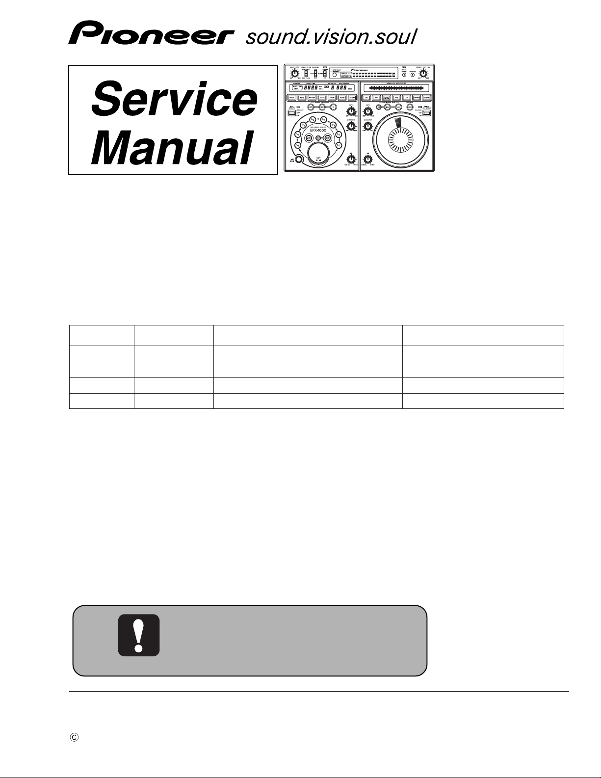
EFX-1000
DJ EFFECTOR
EFX-1000
THIS MANUAL IS APPLICABLE TO THE FOLLOWING MODEL(S) AND TYPE(S).
Model Type Power Requirement Remarks
EFX-1000 KUCXJ AC120V
EFX-1000 TLTXJ AC110 - 240V
EFX-1000 WYXJ AC220 - 240V
EFX-1000 WAXJ AC220 - 240V
For details, refer to "Important Check Points for good servicing".
T-IZY JUNE 2005 printed in Japan
Page 2
1234
SAFETY INFORMATION
A
This service manual is intended for qualified service technicians ; it is not meant for the casual do-ityourselfer. Qualified technicians have the necessary test equipment and tools, and have been trained
to properly and safely repair complex products such as those covered by this manual.
Improperly performed repairs can adversely affect the safety and reliability of the product and may
void the warranty. If you are not qualified to perform the repair of this product properly and safely, you
should not risk trying to do so and refer the repair to a qualified service technician.
WARNING
This product contains lead in solder and certain electrical parts contain chemicals which are known to the state of California to
cause cancer, birth defects or other reproductive harm.
B
NOTICE
(FOR CANADIAN MODEL ONLY)
Fuse symbols (fast operating fuse) and/or (slow operating fuse) on PCB indicate that replacement parts must
be of identical designation.
REMARQUE
(POUR MODÈLE CANADIEN SEULEMENT)
Les symboles de fusible (fusible de type rapide) et/ou (fusible de type lent) sur CCI indiquent que les pièces
de remplacement doivent avoir la même désignation.
C
(FOR USA MODEL ONLY)
1. SAFETY PRECAUTIONS
The following check should be performed for the
continued protection of the customer and service
technician.
ANY MEASUREMENTS NOT WITHIN THE LIMITS
OUTLINED ABOVE ARE INDICATIVE OF A POTENTIAL
SHOCK HAZARD AND MUST BE CORRECTED BEFORE
RETURNING THE APPLIANCE TO THE CUSTOMER.
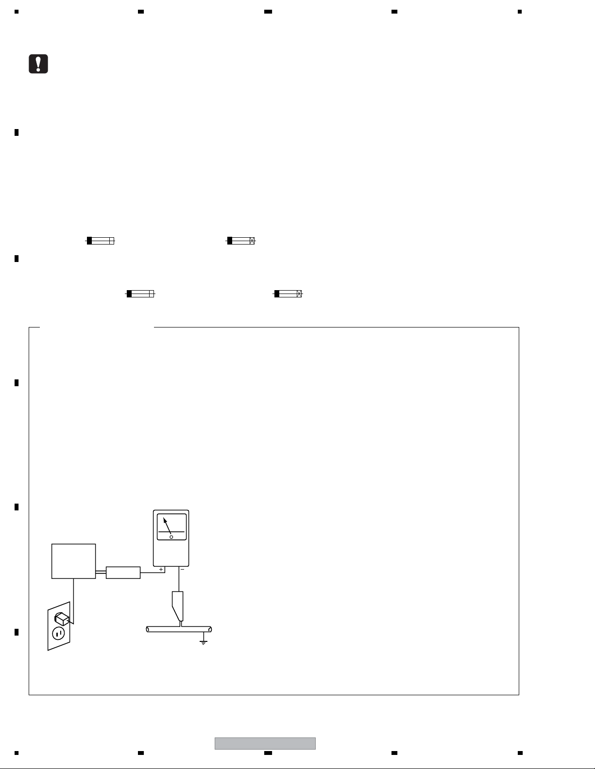
LEAKAGE CURRENT CHECK
Measure leakage current to a known earth ground
(water pipe, conduit, etc.) by connecting a leakage
current tester such as Simpson Model 229-2 or
D
E
equivalent between the earth ground and all exposed
metal parts of the appliance (input/output terminals,
screwheads, metal overlays, control shaft, etc.). Plug
the AC line cord of the appliance directly into a 120V
AC 60 Hz outlet and turn the AC power switch on. Any
current measured must not exceed 0.5 mA.
Reading should
not be above
0.5 mA
Earth
ground
Device
under
test
Also test with
plug reversed
(Using AC adapter
plug as required)
Leakage
current
tester
Test all
exposed metal
surfaces
2. PRODUCT SAFETY NOTICE
Many electrical and mechanical parts in the appliance
have special safety related characteristics. These are
often not evident from visual inspection nor the protection
afforded by them necessarily can be obtained by using
replacement components rated for voltage, wattage, etc.
Replacement parts which have these special safety
characteristics are identified in this Service Manual.
Electrical components having such features are
identified by marking with a > on the schematics and on
the parts list in this Service Manual.
The use of a substitute replacement component which
does not have the same safety characteristics as the
PIONEER recommended replacement one, shown in the
parts list in this Service Manual, may create shock, fire,
or other hazards.
Product Safety is continuously under review and new
instructions are issued from time to time. For the latest
information, always consult the current PIONEER Service
Manual. A subscription to, or additional copies of,
PIONEER Service Manual may be obtained at a nominal
charge from PIONEER.
Health & Safety Code Section 25249.6 - Proposition 65
AC Leakage Test
F
2
1234
EFX-1000
Page 3
5678
[Important Check Points for Good Servicing]
In this manual, procedures that must be performed during repairs are marked with the below symbol.
Please be sure to confirm and follow these procedures.
1. Product safety
Please conform to product regulations (such as safety and radiation regulations), and maintain a safe servicing environment by
following the safety instructions described in this manual.
1 Use specified parts for repair.
Use genuine parts. Be sure to use important parts for safety.
2 Do not perform modifications without proper instructions.
Please follow the specified safety methods when modification(addition/change of parts) is required due to interferences such as
radio/TV interference and foreign noise.
3 Make sure the soldering of repaired locations is properly performed.
When you solder while repairing, please be sure that there are no cold solder and other debris.
Soldering should be finished with the proper quantity. (Refer to the example)
4 Make sure the screws are tightly fastened.
Please be sure that all screws are fastened, and that there are no loose screws.
5 Make sure each connectors are correctly inserted.
Please be sure that all connectors are inserted, and that there are no imperfect insertion.
6 Make sure the wiring cables are set to their original state.
Please replace the wiring and cables to the original state after repairs.
In addition, be sure that there are no pinched wires, etc.
7 Make sure screws and soldering scraps do not remain inside the product.
Please check that neither solder debris nor screws remain inside the product.
8 There should be no semi-broken wires, scratches, melting, etc. on the coating of the power cord.
Damaged power cords may lead to fire accidents, so please be sure that there are no damages.
If you find a damaged power cord, please exchange it with a suitable one.
9 There should be no spark traces or similar marks on the power plug.
When spark traces or similar marks are found on the power supply plug, please check the connection and advise on secure
connections and suitable usage. Please exchange the power cord if necessary.
0 Safe environment should be secured during servicing.
When you perform repairs, please pay attention to static electricity, furniture, household articles, etc. in order to prevent injuries.
Please pay attention to your surroundings and repair safely.
A
B
C
D
2. Adjustments
To keep the original performance of the products, optimum adjustments and confirmation of characteristics within specification.
Adjustments should be performed in accordance with the procedures/instructions described in this manual.
3. Lubricants, Glues, and Replacement parts
Use grease and adhesives that are equal to the specified substance.
Make sure the proper amount is applied.
4. Cleaning
For parts that require cleaning, such as optical pickups, tape deck heads, lenses and mirrors used in projection monitors, proper
cleaning should be performed to restore their performances.
5. Shipping mode and Shipping screws
To protect products from damages or failures during transit, the shipping mode should be set or the shipping screws should be
installed before shipment. Please be sure to follow this method especially if it is specified in this manual.
56
EFX-1000
E
F
3
7
8
Page 4

1234
CONTENTS
1. SPECIFICATIONS ............................................................................................................................................ 5
2. EXPLODED VIEWS AND PARTS LIST ............................................................................................................ 7
A
B
C
2.1 PACKING SECTION .................................................................................................................................. 7
2.2 EXTERIOR SECTION................................................................................................................................ 8
2.3 CONTROL PANEL SECTION .................................................................................................................. 10
3. BLOCK DIAGRAM AND SCHEMATIC DIAGRAM ..........................................................................................12
3.1 BLOCK DIAGRAM ................................................................................................................................... 12
3.2 OVERALL WIRING DIAGRAM................................................................................................................. 18
3.3 MAIN ASSY (1/3) ..................................................................................................................................... 20
3.4 MAIN ASSY (2/3) ..................................................................................................................................... 22
3.5 MAIN ASSY (3/3) ..................................................................................................................................... 24
3.6 CTRL (1/2), SW1 and SW2 ASSYS......................................................................................................... 26
3.7 CTRL ASSY (2/2)..................................................................................................................................... 28
3.8 7SEG ASSY............................................................................................................................................. 30
3.9 MIDI ASSY............................................................................................................................................... 32
3.10 ACIN, ENCB and MVR ASSYS.............................................................................................................. 33
3.11 POWER SUPPLY UNIT.......................................................................................................................... 34
3.12 VOLTAGES............................................................................................................................................. 36
3.13 WAVEFORMS........................................................................................................................................ 38
4. PCB CONNECTION DIAGRAM ..................................................................................................................... 43
4.1 MAIN ASSY ............................................................................................................................................. 44
4.2 CTRL, SW1 and SW2 ASSYS ................................................................................................................. 48
4.3 MIDI, ACIN, ENCB and MVR ASSYS...................................................................................................... 52
4.4 POWER SUPPLY UNIT............................................................................................................................ 54
5. PCB PARTS LIST ........................................................................................................................................... 56
6. ADJUSTMENT ............................................................................................................................................... 71
7. GENERAL INFORMATION............................................................................................................................. 72
7.1 DIAGNOSIS ............................................................................................................................................. 72
7.1.1 TEST MODE ...................................................................................................................................... 72
7.1.2 REWRITING THE FIRMWARE.......................................................................................................... 78
7.1.3 POWER ON SEQUENCE.................................................................................................................. 90
7.1.4 DISASSEMBLY.................................................................................................................................. 92
7.2 PARTS...................................................................................................................................................... 94
7.2.1 IC ....................................................................................................................................................... 94
8. PANEL FACILITIES ........................................................................................................................................ 98
D
E
F
4
1234
EFX-1000
Page 5

5678
1. SPECIFICATIONS
• KUCXJ type
1. General
Power supply ......................................................... AC 120 V, 60 Hz
Power consumption ..................................................................16 W
Operating temperature ................. +5°C to +35°C (+41°F to +95°F)
Relative humidity ....................... 5% to 85% (without condensation)
Weight ........................................................................ 2.4 kg (5.3 lb)
Maximum external dimensions ..... 320 (W) x 234 (D) x 101 (H) mm
12-19/32 (W) x 9-7/32 (D) x 3-31/32 (H) in.
2. Audio Unit
Sampling rate ........................................................................ 96 kHz
A/D, D/A Resolution .............................................................. 24 bits
Frequency characteristics ....................................... 20 Hz to 22 kHz
S/N ratio ................................................................................. 83 dB
Distortion ............................................................................... 0.02 %
Headroom ................................................................................19 dB
Input level ............................................... –10 dBV / +4 dBu (22 kΩ)
Output level ......................................................... –10 dBV / +4 dBu
(RCA pin jacks: 1 kΩ, Phone jacks: 1 kΩ)
*–10 dBV / +4 dBu is switchable.
3. Input/Output terminals
Audio line input terminal
RCA pin jacks ............................................................................ 2
Phone jacks (1/4-inch/6.3 mm in diameter) ............................... 2
Audio line output terminal
RCA pin jacks ............................................................................ 2
Phone jacks (1/4-inch/6.3 mm in diameter) ............................... 2
Digital input terminal
RCA pin jack .............................................................................. 1
Digital output terminal
RCA pin jack .............................................................................. 1
EFX LINK connector (mini-DIN) ..................................................... 1
MIDI input terminal (5-pin DIN) ...................................................... 1
MIDI output terminal (5-pin DIN) .................................................... 1
• TLTXJ type
1. General
Power supply ....................................... AC 110 V - 240 V, 50/60 Hz
Power consumption ..................................................................16 W
Operating temperature .............................................. +5°C to +35°C
Relative humidity ....................... 5% to 85% (without condensation)
Weight .................................................................................... 2.4 kg
Maximum external dimensions ..... 320 (W) x 234 (D) x 101 (H) mm
2. Audio Unit
Sampling rate ........................................................................ 96 kHz
A/D, D/A Resolution .............................................................. 24 bits
Frequency characteristics ....................................... 20 Hz to 22 kHz
S/N ratio ................................................................................. 83 dB
Distortion ............................................................................... 0.02 %
Headroom ................................................................................19 dB
Input level ............................................... –10 dBV / +4 dBu (22 kΩ)
Output level .......................................................... –10 dBV / +4 dBu
(RCA pin jacks: 1 kΩ, Phone jacks: 1 kΩ)
*–10 dBV / +4 dBu is switchable.
3. Input/Output terminals
Audio line input terminal
RCA pin jacks ............................................................................ 2
Phone jacks (1/4-inch/6.3 mm in diameter) ............................... 2
Audio line output terminal
RCA pin jacks ............................................................................ 2
Phone jacks (1/4-inch/6.3 mm in diameter) ............................... 2
Digital input terminal
RCA pin jack .............................................................................. 1
Digital output terminal
RCA pin jack .............................................................................. 1
EFX LINK connector (mini-DIN) ..................................................... 1
MIDI input terminal (5-pin DIN) ....................................................... 1
MIDI output terminal (5-pin DIN) .....................................................1
A
B
C
4. Accessories
Operating instructions .................................................................... 1
Digital link cable ............................................................................. 1
Power cord ..................................................................................... 1
Warranty ......................................................................................... 1
NOTE:
Specifications and design are subject to possible modification
without notice.
4. Accessories
Operating instructions .................................................................... 1
Digital link cable ............................................................................. 1
Power cord ..................................................................................... 1
NOTE:
Specifications and design are subject to possible modification
without notice.
D
E
F
56
EFX-1000
5
7
8
Page 6

1234
• WYXJ type
A
1. General
Power supply ....................................... AC 220 V - 240 V, 50/60 Hz
Power consumption ..................................................................16 W
Operating temperature .............................................. +5°C to +35°C
Relative humidity ....................... 5% to 85% (without condensation)
Weight .................................................................................... 2.4 kg
Maximum external dimensions ..... 320 (W) x 234 (D) x 101 (H) mm
2. Audio Unit
Sampling rate ........................................................................ 96 kHz
A/D, D/A Resolution .............................................................. 24 bits
Frequency characteristics ....................................... 20 Hz to 22 kHz
S/N ratio .................................................................................. 83 dB
B
Distortion ............................................................................... 0.02 %
Headroom ................................................................................19 dB
Input level ............................................... –10 dBV / +4 dBu (22 kΩ)
Output level .......................................................... –10 dBV / +4 dBu
(RCA pin jacks: 1 kΩ, Phone jacks: 1 kΩ)
*–10 dBV / +4 dBu is switchable.
3. Input/Output terminals
Audio line input terminal
RCA pin jacks ............................................................................ 2
Phone jacks (1/4-inch/6.3 mm in diameter) ............................... 2
Audio line output terminal
RCA pin jacks ............................................................................ 2
C
Phone jacks (1/4-inch/6.3 mm in diameter) ............................... 2
Digital input terminal
RCA pin jack .............................................................................. 1
Digital output terminal
RCA pin jack .............................................................................. 1
EFX LINK connector (mini-DIN) ..................................................... 1
MIDI input terminal (5-pin DIN) .......................................................1
MIDI output terminal (5-pin DIN) .....................................................1
• WAXJ type
1. General
Power supply ........................................AC 220 V - 240 V, 50/60 Hz
Power consumption ................................................................. 16 W
Operating temperature .............................................. +5°C to +35°C
Relative humidity ...................... 5% to 85% (without condensation)
Weight .................................................................................... 2.4 kg
Maximum external dimensions...... 320 (W) x 234 (D) x 101 (H) mm
2. Audio Unit
Sampling rate ........................................................................ 96 kHz
A/D, D/A Resolution ............................................................... 24 bits
Frequency characteristics ....................................... 20 Hz to 22 kHz
S/N ratio .................................................................................. 83 dB
Distortion ............................................................................... 0.02 %
Headroom................................................................................ 19 dB
Input level ................................................ –10 dBV / +4 dBu (22 kΩ)
Output level .......................................................... –10 dBV / +4 dBu
(RCA pin jacks: 1 k, Phone jacks: 1 kΩ)
*–10 dBV / +4 dBu is switchable.
3. Input/Output terminals
Audio line input terminal
RCA pin jacks ........................................................................... 2
Phone jacks (1/4-inch/6.3 mm in diameter) ............................. 2
Audio line output terminal
RCA pin jacks ........................................................................... 2
Phone jacks (1/4-inch/6.3 mm in diameter) .............................. 2
Digital input terminal
RCA pin jack ............................................................................. 1
Digital output terminal
RCA pin jack ............................................................................. 1
EFX LINK connector (mini-DIN) ..................................................... 1
MIDI input terminal (5-pin DIN) ...................................................... 1
MIDI output terminal (5-pin DIN) .................................................... 1
4. Accessories
Operating instructions .....................................................................1
Digital link cable ..............................................................................1
Power cord ......................................................................................1
D
NOTE:
Specifications and design are subject to possible modification
without notice.
Accessories
Power cord
(KUCXJ : ADG7021)
(TLTXJ : ADG1127)
(WYXJ : ADG1127)
E
(WAXJ : ADG7079)
Digital link cable
(8P DIN cable)
(DKP3724)
L= 2 m
4. Accessories
Operating instructions .................................................................... 1
Digital link cable ............................................................................. 1
Power cord ..................................................................................... 1
NOTE:
Specifications and design are subject to possible modification
without notice.
Operating Instructions
Warranty (KUCXJ type only)
F
6
1234
EFX-1000
Page 7
>
5678
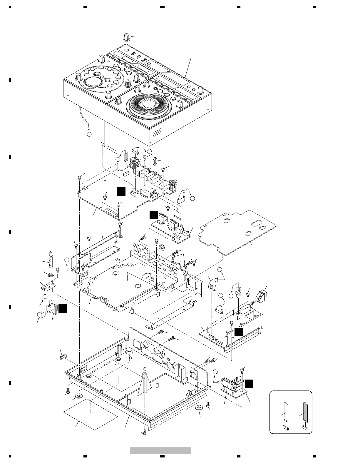
2. EXPLODED VIEWS AND PARTS LIST
NOTES:
Parts marked by "NSP" are generally unavailable because they are not in our Master Spare Parts List.
The mark found on some component parts indicates the importance of the safety factor of the part.
Therefore, when replacing, be sure to use parts of identical designation.
Screws adjacent to mark on product are used for disassembly.
For the applying amount of lubricants or glue, follow the instructions in this manual.
(In the case of no amount instructions, apply as you think it appropriate.)
2.1 PACKING SECTION
7
9
11
A
3
2
1
5
KUCXJ
12
Only
4
WYXJ
6
Only
B
C
8
10
(1) PACKING SECTION PARTS LIST
No. Description Part No.
No. Description Part No.
Mark
1Powe Cord See Contrast table (2)
NSP 2 Polyethylene Bag AHG7117
3 Digital Link Cable(8P DIN Cable)DKP3724
4 Operating Instructions See Contrast table (2)
NSP 5 User Registration SH DRM1262
Mark
6 WEE Caution Card See Contrast table (2)
7Pad (A) DHA1645
8Pad (B) DHA1687
9Pad (C) DHA1647
10 Packing Case See Contrast table (2)
11 Sheet RHX1006
NSP 12 Limited Warranty See Contrast table (2)
(2) CONTRAST TABLE
EFX-1000/KUCXJ, TLTXJ, WYXJ and WAXJ are constructed the same except for the following:
Mark No. Symbol and Description
>
NSP 12 Limited Warranty ARY7043 Not used Not used Not used
1Power Cord ADG7021 ADG1127 ADG1127 ADG7079
4 Operating Instructions (Chinise/English) DRB1367 Not used Not used Not used
4 Operating Instructions (English/Spanish/ Chinese) Not used DRB1369 Not used Not used
4 Operating Instructions (English/French/Duch/German/Italian/Spanish) Not used Not used DRB1368 Not used
4 Operating Instructions (English) Not used Not used Not used DRB1370
6 WEE Caution Card Not used Not used ARM7099 Not used
10 Packing Case DHG2476 DHG2477 DHG2475 DHG2479
EFX-1000/
KUCXJ
EFX-1000
56
7
EFX-1000/
TLTXJ
EFX-1000/
WYXJ
EFX-1000/
WAXJ
8
D
E
F
7
Page 8
1234
2.2 EXTERIOR SECTION
A
B
A
29
18
Refer to
"2.3 CONTROL PANEL SECTION" .
C
29
B
17
31
31
C
1
13
29
15
D
26
14
B
A
30
I
4
6
E
20
29
29
16
A
29
29
30
F
29
29
28
28
27
28
28
D
3
31
23
19
28
29
30
7
29
D
8
C
E
9
5
29
J
30
30
30
E
G
12
F
22 21
8
1234
30
EFX-1000
12
10
30
2
NON-CONTACT
SIDE
CONTACT SIDE
Page 9
>
>
5678
(1) EXTERIOR SECTION PARTS LIST
No. Description Part No.
Mark
1 MAIN BOARD Assy DWX2401
2ACIN Assy See Contrast table (2)
3 MIDI Assy DWX2402
4 MVR Assy DWX2444
5POWER SUPPLY Unit DWR1377
No. Description Part No.
Mark
16 Main Shield Assy DXB1851
NSP 17 PCB Holder REC1220
18 Knob VOL DAA1168
19 Power Knob DAC1895
20 Blind Cap DNK4218
A
6 10P Flexible Cable DDD1293
NSP 7 Earth Lead Wire DE005VF0
8 Connector Assy DKP3725
9 Connector Assy DKP3741
10 Ferrite Core DTH1196
11 • • • • •
12 Insulator MO DEC2250
13 Insulation Sheet B DEC2823
14 VOL Support Plate MASTER DNF1719
15 Extension Shaft DNK4348
NSP 21 Chassis See Contrast table (2)
22 Block Label DRW2271
23 E Wave Sheet DEC2881
24 • • • • •
25 • • • • •
26 Nut M7 DBN1011
27 Nut M12 DBN1012
28 Screw PMH30P100FTB
29 Screw BBZ30P060FTB
30 Screw BPZ30P080FTB
31 Screw BBZ30P080FTC
(2) CONTRAST TABLE
EFX-1000/KUCXJ, TLTXJ, WYXJ and WAXJ are constructed the same except for the following:
Mark No. Symbol and Description
2ACIN Assy DWR1382 DWR1381 DWR1381 DWR1381
NSP 21 Chassis DNK4618 DNK4621 DNK4617 DNK4620
EFX-1000/
KUCXJ
EFX-1000/
TLTXJ
EFX-1000/
WYXJ
EFX-1000/
WAXJ
B
C
D
E
F
56
EFX-1000
9
7
8
Page 10
1234
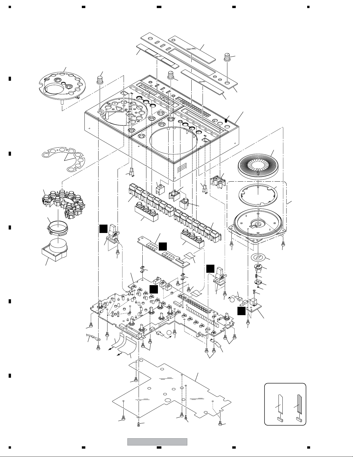
2.3 CONTROL PANEL SECTION
A
34
38
B
36
C
31
39
22
D
40
21
30
28
23
26
1
40
33
21
32
35
37
44
17
29
45
20
25
24
3
D
41
47
2
E
11
B
27
47
11
47
14
43
47
15
18
19
47
6
C
10
4
A
47
16
H
5
47
E
9
MAIN CN102
F
47
To
MAIN CN402
7
To
47
8
47
42
47
A
47
47
13
47
12
47
42
47
47
NON-CONTACT
SIDE
CONTACT SIDE
10
EFX-1000
1234
Page 11

5678
CONTROL PANEL SECTION PARTS LIST
Mark
No. Description Part No.
1 7SEG Assy DWG1584
2 CTRL Assy DWG1585
3 SW1 Assy DWS1353
4 SW2 Assy DWS1354
5 ENCB Assy DWX2403
6 20P Flexible Cable DDD1274
7 10P Flexible Cable DDD1290
8 28P Flexible Cable DDD1292
NSP 9 Earth Lead Wire DE015VF0
10 Small Connector PF04PP-C05
A
11 PC Support DEC2736
12 Insulation Sheet A DEC2807
13 Earth Plate (CU) VBK1070
14 JOG Spring DBH1540
15 Encoder Plate DEC2498
16 Nyron Rivet DEC2735
17 JOG Dial DNK4337
18 Encoder Holder DNK4339
19 Smoother DNK4346
20 JOG Holder Assy DXA1992
21 Knob VOL DAA1168
22 Knob TIME DAA1169
23 Button Effect DELAY DAC2223
24 Button Effect JET DAC2224
25 Button MEMORY DAC2225
26 Button HOLD DAC2226
27 Button LOW DAC2227
28 Button METER DAC2228
29 Button LB DAC2229
30 Slide Knob DAC2230
31 Button BEAT DAC2231
32 aluminum Panel DAH2330
33 Window LEVEL DAH2331
34 Window TIME DAH2332
35 Window JOG DAH2333
B
C
D
36 Sheet DED1175
37 Control Panel DNK4340
38 Escutcheon DNK4342
39 TAP Display Ring DNK4343
40 Indicator DNK4344
41 Button TAP Assy DXA1993
42 Nyron Rivet 3x4.5 RBM-003
43 Washer WT26D060D050
44 Earth Spring DBH1539
45 Pom Ring DNK4345
46 Screw BBZ30P060FTB
47 Screw BPZ30P080FTB
56
EFX-1000
E
F
11
7
8
Page 12
2
4
6
8
0
1234
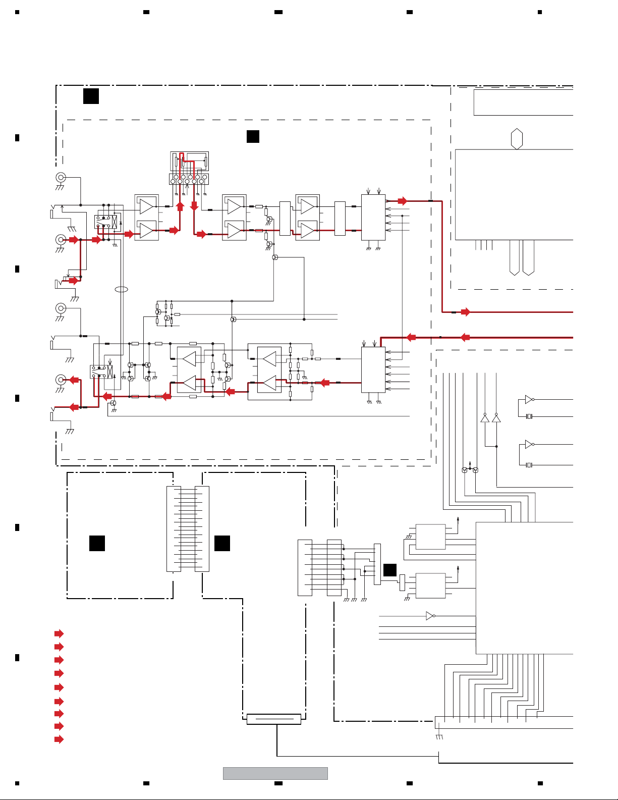
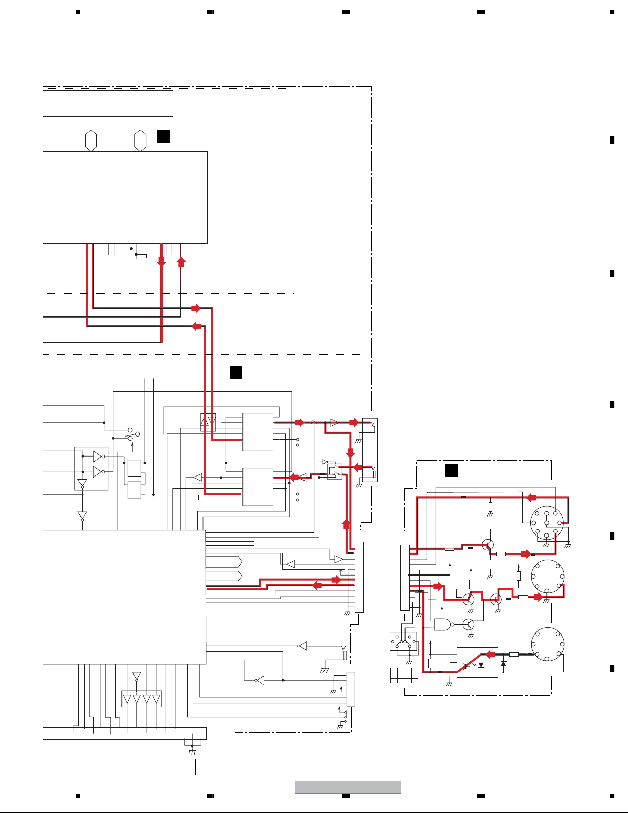
3. BLOCK DIAGRAM AND SCHEMATIC DIAGRAM
3.1 BLOCK DIAGRAM
A
• AUDIO BLOCK
B
C
D
E
F
R IN
(RCA)
R IN
(PHONE)
L IN
(RCA)
L IN
(PHONE)
R OUT
(RCA)
R OUT
(PHONE)
L OUT
(RCA)
L OUT
(PHONE)
(MID)
(DIG)
(EFX)
(DS_SRC)
(SRC_DS)
(DS_DA)
(DS_AD)
(HP)
A
MAIN BOARD ASSY
VR1201
INPUT TRIM VR
4
10
6
(HP)
(HP)
RY301
VSR1008
L CH
R CH
VSR-1008
4
7
3
4
89
7
RY201
3
89
BYPASS
LINE
V+12
2
V+12
2
10
2
3
1
R CH
6
7
5
8
2
3
IC201
NJM4580MD
Q302
Q301
L CH
R CH
+15V
4
-15V
1
L CH
Q204 Q205
Q304
Q303
+15V
-15V
+15V
-15V
1
8
4
7
IC303
NJM4580MD
1
10
1
Q307
V3R3
CN200
789
5
6
R CH
5
2
3
L CH
IC202
NJM4580MD
2
3
6
5
CN715CN601
1
1
2
3
5
7
9
-
~
E B
7SEG ASSY CTRL ASSY
@
$
^
2
3
4
4
5
6
6
7
8
0
=
!
#
%
&
"Refer to Control Block""Refer to Control Block"
8
9
0
=
~
!
@
#
$
%
^
&
: AUDIO SIGNAL ROUTE (Digital Signal (MIDI))
: AUDIO SIGNAL ROUTE (Digital Signal)
: SIGNAL ROUTE (EFX LINK)
: AUDIO SIGNAL ROUTE (Digital Signal (DSP to SRC)
: AUDIO SIGNAL ROUTE (Digital Signal (SRC to DSP)
: AUDIO SIGNAL ROUTE (Digital Signal (DSP to D/A)
: AUDIO SIGNAL ROUTE (Digital Signal (A/D to DSP)
: AUDIO SIGNAL ROUTE (Phones L ch)
: AUDIO SIGNAL ROUTE (L ch)
A
1/3 MAIN BOARD ASSY
300kHz
LPF
Q202
7
8
+15V
4
-15V
1
Q298
R CH
1
Q306
+15V
8
4
-15V
Q305
7
L CH
IC301
NJM4580MD
1£
Q201
6
5
2
3
IC203
NJM4580MD
Q299
2
3
6
5
1
2
3
4
5
6
7
8
9
0
CN705
V3R3: 1,3,9,14,27,43,49
GND : 6,12,28,4146,52
DQ 6
DQ 7
DQ 8
DQ 9
DQ10
DQ11
DQ12
DQ13
DQ14
DQ15
ED10
ED11
ED12
ED13
ED14
ED15
113
112
V+5A V3R3
300kHz
LPF
R CH
7
8
+15V
4
-15V
1
L CH
MUTE
GAINSWOUT
R CH
L CH
CN102CN701
1
1
2
2
3
3
4
4
5
5
6
6
7
7
8
8
9
9
0
0
HRDYn
DSPCSn
DSPRST1n
DSPINTn
6 7
R CH
1
2
L CH
5 8
IC200
AK5381VT
V+5A V3R3
6 5
8
R CH
7
L CH
4 9
IC300
PCM1742KE
CN101
(DS_AD)
9
13
11
12
10
ADCDT
ADRSTN
SCK
AD_64FS
AD_96K
(DS_DA)
BCK
1
16
15
14
13
1
2
3
4
5
6
7
8
LRCK
3
DAMLN
TSRCCK
TSRCTXD
BYPASS
IC415
BR93L66F-W
8
7
6
5
TO POWER SUPPLY UNIT
(CN201)
IC417
M51957BFP
J
1
L
2
P
3
F
4
6 2
VCC:4
GND:8
D610A002BPY225-K
176
135
DSPRST1n
DSPINTn
DIGITAL SIGNAL(A/D To DSP)
(DS_AD)
DACDT
DIGITAL SIGNAL(DSP To D/A)
(DS_DA)
DAMLN
DVL
ADRSTn
BYPASS
MUTE
TC7SU04F
V3R3
Q411
Q401
V3R3
1
2
56
3
52
4
57
58
V3R3
8
7
92
6
5
IC404
1
84
TC7WH04FU
108
110
135
357 9 - ~
246 8 0 =
ED 9
119
120
117
118
111
IC500
140
145
HRDYn
DSPCSn
CLKIN(DPS)
SCK(A/D)
IC503
IC310
TC7SU04F
GND:3
VCC:5
24
24
474927
ED 6
ED 7
ED 8
121
122
123
81
121
122
HA1-4
22.5792Mhz
90
123
1011134244454748505153
DQ 4
DQ 5
DE 4
ED 5
127
128
IC416
2
TC7SU04F
X401
1
TC7WH04F
120
124
DQ 2
DQ 3
ED 2
ED 3
130
129
HD0-15
IC409
GND:4
VCC:8
106
125
126
DQ 1
ED 1
131
4
7
127
24578
DQ 0
ED 0
132
GND:3
VCC:5
3
19
CS
CE0
102
128
115
12
SS6
SS4
SS5
SS7
TMCW
TMCCW
DISPCONTn
SS0
SS1
SS2
SS3
BEATMIX
EFX-1000
1234
Page 13
5678
IC411
IC411
IC501
K4S281632F-UC-75-K
39
RAS
CASWELDQM
UDQM
SDWEn
SDCAS
SDRAS
BE0
BE1
108
V3R3B: 5,9,25,44,47,55,58,65,72,84,87,96,107,114,126,141,162,183,188,206
V1R2 : 3,11,14,22,29,35,40,43,46,50,51,53,60,67,80,89,96,104,105,116,124
: 133,149,157,169,171,177,181,190,195,196,201,208
GND : 4,10,15,23,26,30,34,39,45,48,49,54,59,66,73,81,85,88,97,106,115,125
: 134,142,148,158,163,170,182,189,184,199,203,207
20
27
OUTSRCDT
INSRCDT
ECLKOUT
EA15
151
204
DSPRDN
DSPCLK
A10
A11
BA0BACLK
EA12
EA13
EA14
150
DSPWRN
A 8
A 9
EA10
EA11
21,24,38
64FS
96kHz
A 4
A 5
A 6
A 7
EA 6
EA 7
EA 8
EA 9
8,16,19,36
AD_64FS
23242526293031323334223520213818171615
A 0
A 1
A 2
A 3
A
3/3 MAIN BOARD ASSY
EA 2
EA 3
EA 4
EA 5
626364686970717476869391909477757983110
333132
37
BCK
LRCK
AD_96k
(DS_AD)
DACDT
ADCDT
A
B
(DS_DA)
DIGITAL SIGNAL(DSP To SRC)
DIGITAL SIGNAL(SRC To DSP)
(SRC_DS)
64fs
96kHz
IC410
TC74VHC00F
GND:7
VCC:1
10
11
IC405
3 5
6 2
TC7WH04F
7 1
IC418
GND:3
4 2
VCC:5
97
119
114
118
@$ ^ * ) + ™
!
#%& (_¡£
4
1,2,9
IC413
2211
15
7
96kHz
IC414
1,7,9,10,16:V3R3
IC413
3,4,5,6,8:GND
1,9,10,16:V3R3
IC414
3,4,5,6,8:GND
51
IC400
PEG097A8-K
(HD64F2377-K)
VCC:4,41,72,98,99,111,112
VSS:2,10,18,25,40,50,70,95,102,129
116
142
3 2
IC411
TC74VHC125FTS
IC404
7 1
6 5
138
TC7WHU04FU
11 12
113
117
TC74VHC161FT
23
24
VCC:4
GND:8
8 9
IC411
VCC:14
RSCRSTn
TSCRSTn
131
130
63,64,65,66,67,68,69,71
73,74,75,76,77,78,79,80
45
44
GND:7
JGMIX
BEATCHR
JGCHR
BEATDPT
JGDPT
EFOUTLEVEL
EXPOUT
EXPCLK
EXPSTBn
EXPBLK
JGA
JGB
56
IC407
6.14MHz
IC407
TSRCRXD
TSRCCSn
83
(DS_SRC)
INSRCDT
12 11
3 2
RSRCCSn
59
826133
133
134
6,7,8,11
26
54
55
42
43
28
141
139
OUTSRCDT
TC74VHC125FT
6 5
GND:7
VCC:14
TC74VHC125FT
TSRCCK
TSRCTXD
DIG MUTE
30
DIGINSEL
60
88
89
HD0-15
HA1-4
14
143,144
1
CN402
A
2/3 MAIN BOARD ASSY
IC401
CS8420-CSZD1
ISCLK
13
1
SDA
2
AD0
RST
9
14
SDIN
12
ILRCK
CS8420-CSZD1
16
OSCLK
1
SDA
2
AD0
9
RST
18
SDOUT
16
OLRCK
MIDI OUT
IC402
DSPWRN
DSPRDN
OMCK
CCLK
OMCK
CDIN
CCLK
CDIN
RXP
21
26
TXP
27
28
6,23
7,22
21
4
27
28
6,23
7,22
MIDI IN
6 5
V+5D1
GNDA
Q409
(DIG)
V+5D2
GNDA
Q412
Q403
TC7W66FU
IC412
TC74VHC125FTS
VCC:14
(MID)
GND:7
(MID)
Q405
Q408
Q400
(DIG)(DIG)
(EFX)
3
(DIG)
6 5
1 2
7
IC403
VCC:8
GND:4
(EFX)
J403
VCC:8
GND:4
1
2
12 11
3
4
5
6
7
8
9
0
=
S1000
JA401
FOOT SW
CN400
6
GND
FLWR
5
NC
4
V3R3
3
REM1
2
REM2
1
-10dB
+ 4dB
S201
EFX-1000
DIGITAL OUT
JA400
DIGITAL IN
CN1001
MINI DIN
TXD
DIN
MIXRXD
GND
+5V
MIDI PASS
MIDI TXD
MIDI RXD
FSEL1
FSEL2
GND
9
8
7
1,5
6,10
6,10
96k48k 44k
1
2
3
4
5
6
7
8
9
0
=
1,5
HLL
HHL
7
C
F
MIDI ASSY
(EFX)
R1020
180
V+5D1
R1013
Q1002
1k
V+5D1
V+5D1
(MID)
Q1003
V+5D1
5
4
2
1
IC1002
3
4
2
TC7SH08FU
V+5D1
3
6
R1001
5
R1008
560
4
R1010
220
Q1001
IC1001
PC900V0NSZX
(MID)
R1009
1
2
68
Q1000
(EFX)
V+5D1
R1004
220
D1002
1SS355
R1003
220
R1002
220
8
5 3
2
GNDF GNDD1
6
1
4
(MID)
6
1
4
7
6
4
EFX LINK
1
9
7
3
MIDI OUT
5
2
7
3
MIDI IN
5
2
D
E
F
13
8
Page 14
1234
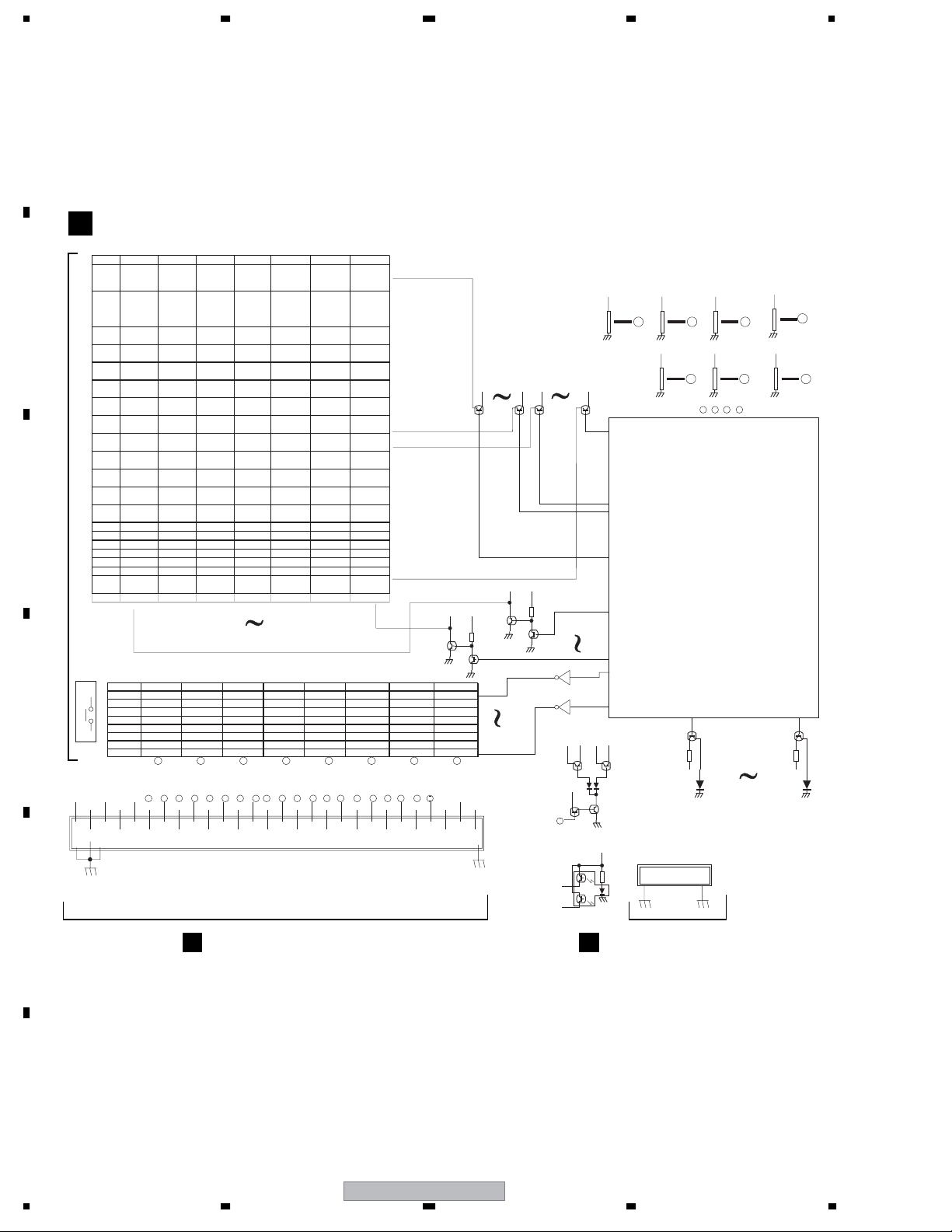
• CONTROL BLOCK
A
B
CTRL ASSY
B
C
Refer to next page
D
E
(EXP.)
SS7 KSC0
1 3 5 7 9 11 13 15 17 19 21 23 25 27
2 4 6 8 10 12 14 16 18 20 22 24 26 28
LED MATRIX
KEY MATRIX
A B C D E F G H
J K L M N O P Q R S T
JGDPT
EFOUTLEVEL
EXPOUT
EXPCLK
EXPSTBn
EXPBLK
JGA
JGB
JGCHR
BEATDPT
A B C D E F G H
SS7
BEATMIX
JGMIX
BEATCHR
SS6
SS5
SS4
SS3
SS2
SS1
Q702
I
DISPCONTn
SS0
SEG19
Q721 Q728
SEG12
SEG11
V+12ADIG 7
TMCW
TMCCW
V+12A
Q716
Q762
CN705
V+5A
V+12A
Q729
V+12ADIG 0
Q769
IC703
TC74VHC04FS
Q717 Q718
D105
RPI-2150N
JOG A
JOG B
V3R3
V+5A
Q740
SEG0
V+12A
V+ 5A
V+ 5D
D722
V3R3
I
V+ 5A
VR701
EFFECT OUT
LEVEL
51 SEG 0
52 SEG 1
23 SEG 2
24 SEG 3
55 SEG 4
56 SEG 5
57 SEG 6
58 SEG 7
59 SEG 8
60 SEG 9
61 SEG10
62 SEG11
63 SEG12
64 SEG13
65 SEG14
66 SEG15
67 SEG16
68 SEG17
69 SEG18
70 SEG19
83 DIG 0
84 DIG 1
85 DIG 2
86 DIG 3
87 DIG 4
88 DIG 5
89 DIG 6
90 DIG 7
91 KSC 0
92 KSC 1
93 KSC 2
94 KSC 3
95 KSC 4
96 KSC 5
V+12
Q720Q719
V3R3
DEPTH
N
V3R3
JOG DEPTH
V3R3
GNDL
GNDL
GNDL
GNDF
1 3 5 7 9
2 4 6 8 10
VR702
BEAT
VR703
V3R3
2.2k
V+5D
P
O
BK0
41
V+12A
V+5D
V3R3
V3R3
J K L M
EXPBLK 45
UPD16306B
BK 1
BK 2
8
9
BK0
D842
V+12
V+12
CHARACTER
CHARACTER
EXPSTBn 43
IC705
BK 3
BK 4
10111213141516171819202122
CN701
VR704
BEAT
R
VR705
JOG
Q
EXPOUT 36
EXPCLK 38
BK 5
BK 6
BK 7
BK 8
BK 9
BK10
V3R3
V3R3
BK11
BK12
BK13
VR706
BEAT MIX
VR707
JOG MIX
BK14
BK15
2.2k
V+12A
T
S
BK16
23
BK16
D858
TO MAIN BOARD ASSY (CN402) TO MAIN BOARD ASSY (CN102)
A A
F
14
EFX-1000
1234
Page 15
E
7SEG ASSY
5678
A
TIME
4/4
1
10
2
9
3
8
7
4
56
D615
TIME
3/4
1
10
2
9
3
8
7
4
56
D614
TIME
2/4
1
10
2
9
3
8
7
4
56
D613
TIME
1/4
1
10
2
9
3
8
7
4
56
D612
RHYTHM
COUNT
1
2
3
4
56
D619
BPM
10
9
8
7
3/3
1
10
2
9
3
8
7
4
56
D618
AUTO MANU
D601
D602
D603
D604
BPM
2/3
1
10
2
9
3
8
7
4
56
D617
RHYTHM
D605
D606
D608
D620
MIDI
BPM
1/3
1
10
2
9
3
8
4
7
5
6
D616
5 SEG4
4 SEG3
3 SEG2
2 SEG1
1 SEG0
6 SEG5
7 SEG6
8 SEG7
17 DIG7A
16 DIG6A
15 DIG5A
14 DIG4A
12 DIG3A
11 DIG2A
10 DIG1A
9 DIG0A
18 SEG16
13 SEG17
B
C
TO CTRL ASSY (CN715)
B
20 DIG4
19 DIG3
CN601
D
56
EFX-1000
E
F
15
7
8
Page 16

1234
A
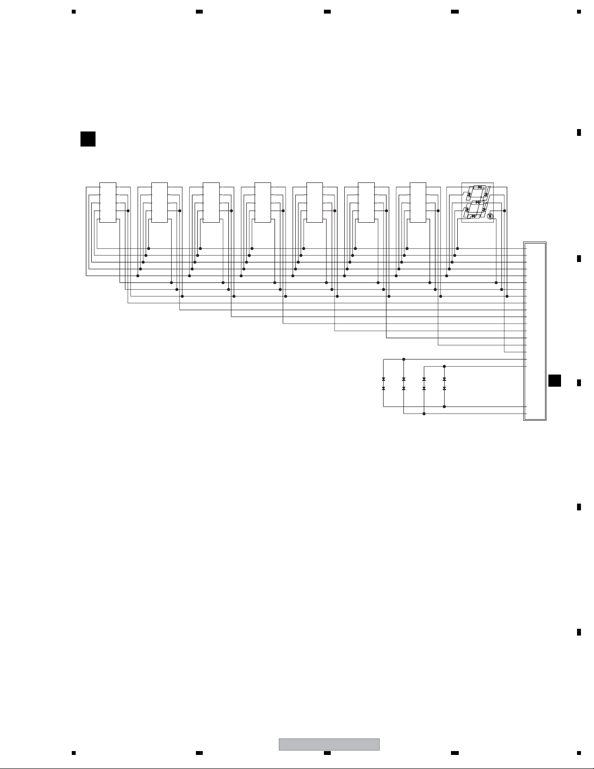
LED Matrix
SEG23 - SEG20 SEG19 SEG18 SEG17 SEG16 SEG15 SEG14 SEG13 SEG12 SEG11
PHASE
DIG0
DIG1
− RING-LP
−−
SHIFTER-
LP
VOCODER
-LP
WAH-LP JET-LP LMUP07 LMUP06 LMUP05 LMUP04 LMUP03
HUMANIZER
-LP
ZIP-LP − LMUP14 LMUP13 LMUP12 LMUP11
B
C
D
DIG2
DIG3
DIG4
DIG5
DIG6
DIG7
Key Matrix
KSC0
KSC1
KSC2
KSC3
KSC4
KSC5
KSC6
KSC7
−
−−−RYTH-DS TAP-DS − LMDW14 LMDW13 LMDW12 LMDW11
−−−MIDI-DS AUTO-DS HOLD-LP AUTO-LP PLAY-LP − LMR-LP
− TAPB-LP TAPB-LP TAPB-LP TAPB-LP -1/2R-LP -8/1R-LP -4/1R-LP -2/1R-L 8/1R-LP
− TRNS-LP
− RYTH-LP PHAS-LP FILT-LP FLAN-LP LOW-LP MID-LP HI-LP − JEF-ON
LMOUT-
LP
LMIN-LP LINK-LP − LMDW07 LMDW06 LMDW05 LMDW04 LMDW03
PICH
ECHO-LP
ECHO-LP DELY-LP -1/1R-LP -3/4R-LP -1/4R-LP -1/8R-LP 3/4R-LP
SS7 SS6 SS5 SS4 SS3 SS2 SS1 SS0
EFFECT MIDI BYPASS LINK METER FTJO-SW FTBT-SW BLK-SEL
PHAS FILT TRAN FLAN PAN ECHO DELAY BEATSW
8/1 4/1 2/1 1/1 3/4 1/2 1/4 1/8
MEMO
AQUA REVE HAMO RING WAH ZIP JET JOGSW
− −−−
− −−−−−−−
− −−−−−−−
−
TAPSW RHMSW BPMSW HI MID LOW
HOLDSW JAUTOSW PLAYSW MEMOSW
E
F
16
1234
EFX-1000
Page 17

5678
SEG10 SEG9 SEG8 SEG7 SEG6 SEG5 SEG4 SEG3 SEG2 SEG1 SEG0
LMUP02 LMUP01 LMUP00 BPM1-LP −−−−−−BPM1-LP
LMUP10 LMUP09 LMUP08 BPM2-LP −−−−−−BPM2-LP
LMDW02 LMDW01 LMDW00 BPM3-LP −−−−−−BPM3-LP
A
LMDW10 LMDW09 LMDW08 RYT1-LP −−−−−−RYT1-LP
LML-LP
4/1R-LP 2/1R-LP 1/1R-LP TM2-LP −−−−−−TM2-LP
1/2R-LP 1/4R-LP 1/8R-LP TM3-LP −−−−−−TM3-LP
BEF-ON BPM-LP +8/1R-LP TM4-LP −−−−−−TM4-LP
BYPASS-
LP
− TM1-LP −−−−−−TM1-LP
B
C
D
56
EFX-1000
E
F
17
7
8
Page 18
1234
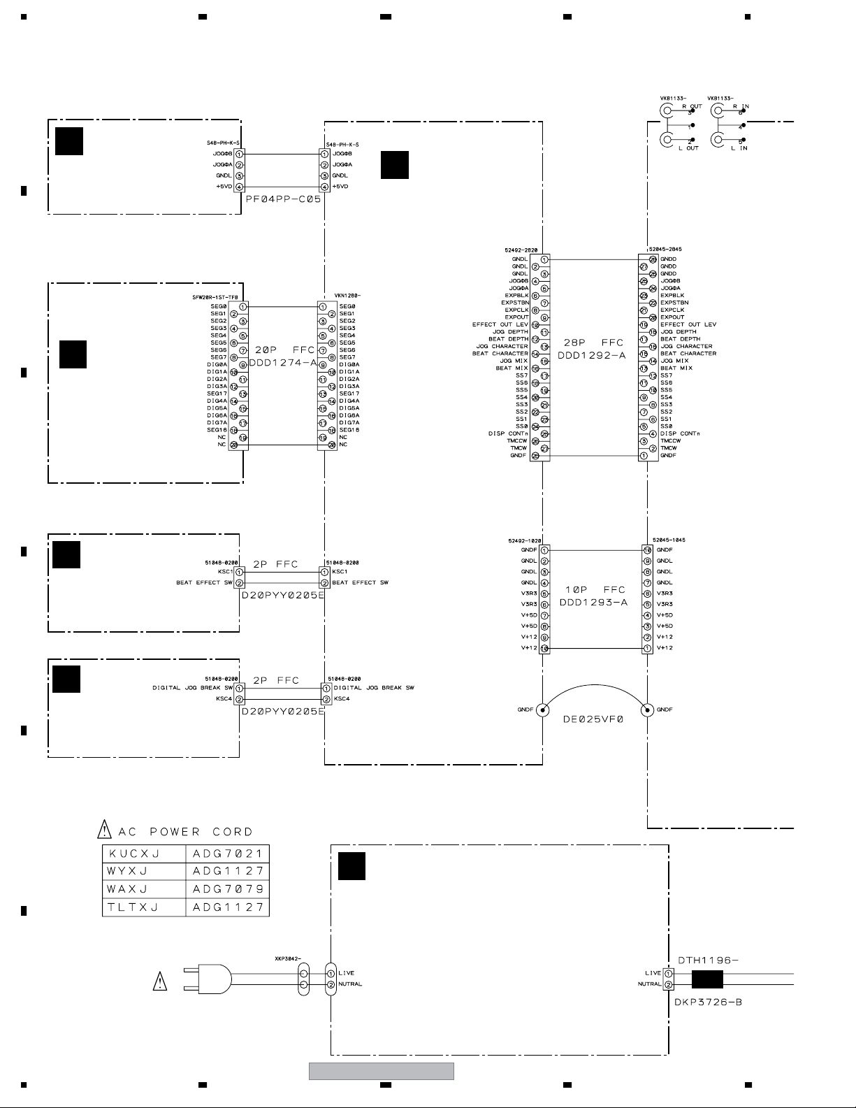
3.2 OVERALL WIRING DIAGRAM
A
H
ENCB ASSY
(DWX2403)
B
E
7SEG ASSY
(DWG1584)
C
CN104
CN601
4P CONNECTOR
CABLE
CN713
CN715
B
CTRL ASSY
(DWG1585)
CN705
JA301 JA301
CN402
D
SW1 ASSY
(DWS1353)
D
C
SW2 ASSY
(DWS1354)
E
F
J701
J702 J902
AC POWER CORD
CN701
J901
GND CABLE
ACIN ASSY
G
WYXJ,TLTXJ,WAXJ: (DWR1381)
KUCXJ: (DWR1382)
AN1101
AN1101
AN1101
WYXJ, TLTXJ, WAXJ: XKP3041
KUCXJ: XKP3042
CN102
J1101
J1102
TERRITE CORE
2P CONNECTOR
CABLE
18
EFX-1000
1234
Page 19
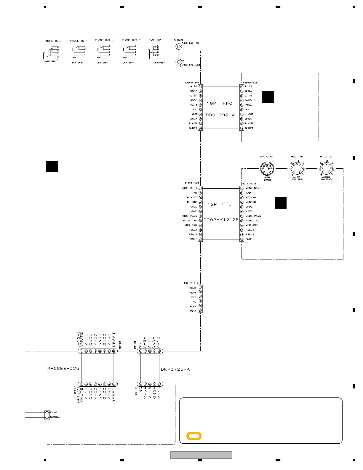
5678
JA201 JA202 JA302 JA303
MAIN BOARD ASSY
A
(DWX2401)
JA401
JA400
CN200
J403
CN201
CN1001
I
MVR ASSY
(DWX2444)
F
A
B
C
8P CONNECTOR
CABLE
CN101
CN100CN202
5P CONNECTOR
CABLE
MIDI ASSY
(DWX2402)
D
CN400
E
CN101
CN201
POWER SUPPLY
(DWR1377)
56
÷
When ordering service parts, be sure to refer to "EXPLODED
VIEWS and PARTS LIST" or "PCB PARTS LIST".
÷
The > mark found on some component parts indicates the
importance of the safety factor of the part. Therefore, when
replacing, be sure to use parts of identical designation.
÷
: The power supply is shown with the marked box.
EFX-1000
F
19
7
8
Page 20
1234
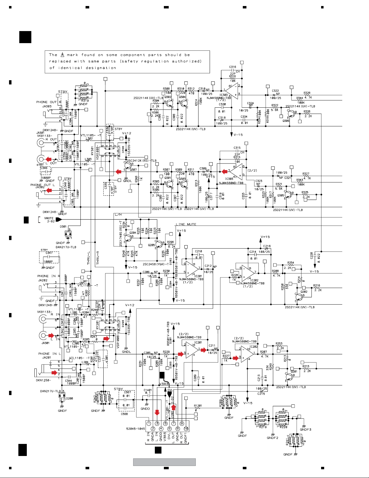
3.3 MAIN ASSY (1/3)
MAIN BOARD ASSY (1/3) (DWX2401)
A
A
B
(HP)
C
2/3A
D
E
F
20
A 1/3
(HP)
2/3A
CN200
CN1201
I
EFX-1000
1234
Page 21
5678
(MID)
: AUDIO SIGNAL ROUTE (Digital Signal (MIDI))
(DIG)
: AUDIO SIGNAL ROUTE (Digital Signal)
(EFX)
: SIGNAL ROUTE (EFX LINK)
(DS_SRC)
: AUDIO SIGNAL ROUTE (Digital Signal (DSP to SRC)
(SRC_DS)
: AUDIO SIGNAL ROUTE (Digital Signal (SRC to DSP)
(DS_DA)
: AUDIO SIGNAL ROUTE (Digital Signal (DSP to D/A)
(DS_AD)
: AUDIO SIGNAL ROUTE (Digital Signal (A/D to DSP)
(HP)
: AUDIO SIGNAL ROUTE (Phones L ch)
: AUDIO SIGNAL ROUTE (L ch)
(DS_DA)
3/3A
(DS_DA)
A
3/3A
B
2/3
A
C
(DS_AD)
(DS_AD)
A
2/3A
D
2/3
3/3A
E
J
CN202
CAUTION : FOR CONTINUED PROTECTION AGAINST
RISK OF FIRE. REPLACE ONLY WITH
SAME TYPE NO. ICP-N15, MFD BY ROHM
CO., LTD. FOR IC100.
CAUTION : FOR CONTINUED PROTECTION AGAINST
RISK OF FIRE. REPLACE ONLY WITH
SAME TYPE NO. AEK7005 MFD, BY
LITTELFUSE INK. FOR IC101and IC102.
EFX-1000
56
CN100
F
A 1/3
21
7
8
Page 22
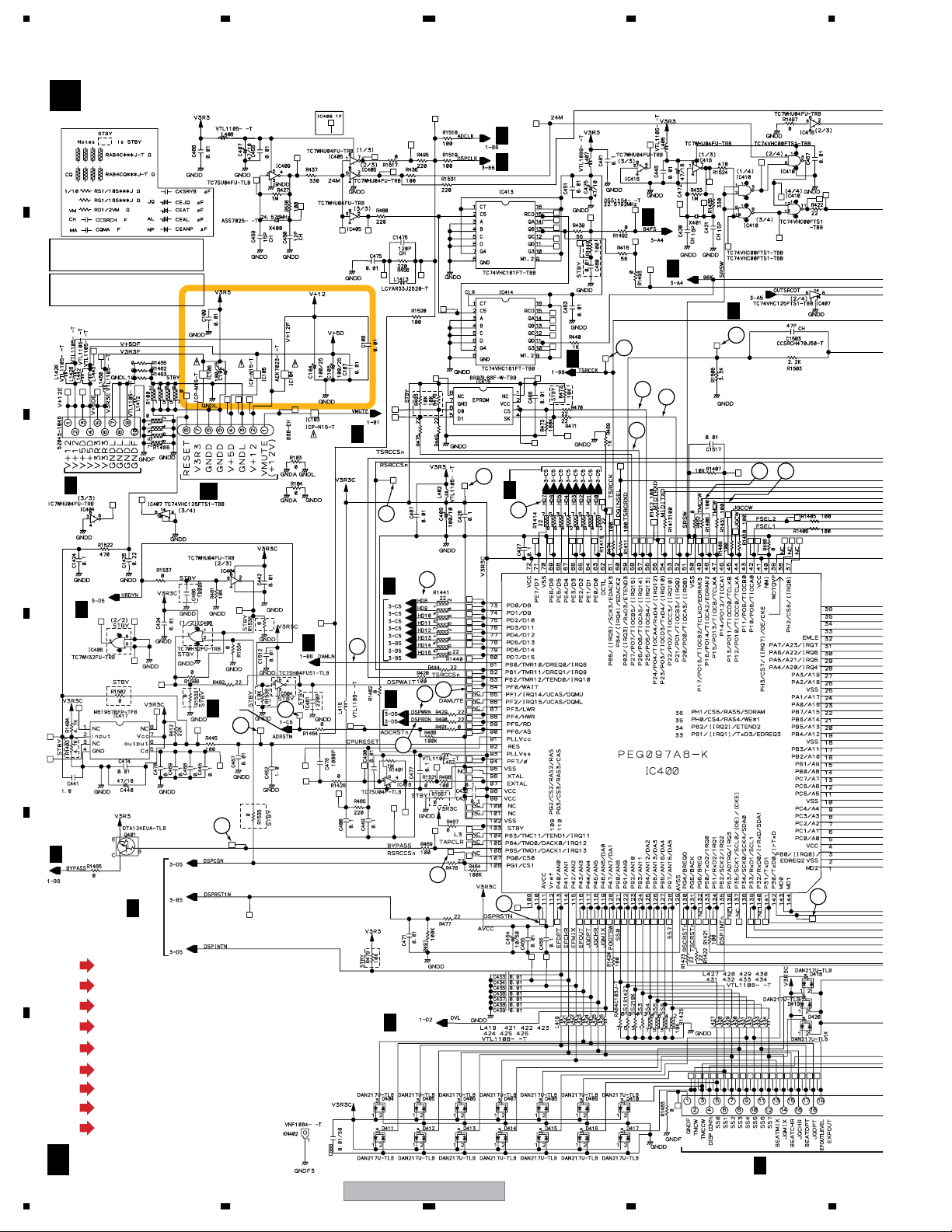
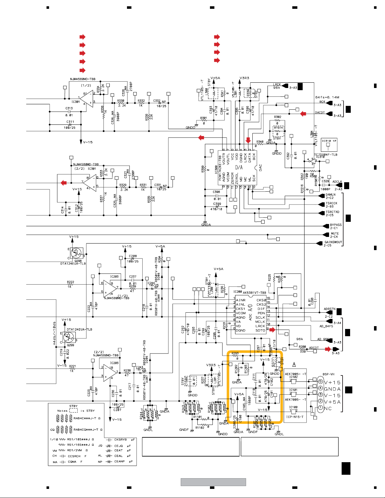
1234
3.4 MAIN ASSY (2/3)
MAIN BOARD ASSY (2/3) (DWX2401)
A
A
CAUTION : FOR CONTINUED PROTECTION AGAINST
RISK OF FIRE. REPLACE ONLY WITH
SAME TYPE NO. ICP-N15, MFD BY ROHM
CO., LTD. FOR IC103, IC105 and IC106.
CAUTION : FOR CONTINUED PROTECTION AGAINST
RISK OF FIRE. REPLACE ONLY WITH
SAME TYPE NO. AEK7023 MFD, BY
LITTELFUSE INK. FOR IC104.
B
1/3
A
3/3
A
A
3/3
3/3A
A
3/3
15b
12b
1/3A
16a
16b
A
15a
1/3
1a
1/3A
8a
18b
3/3
A
22a
18a
3/3A
20a
18b
CN102
CN701
1/2
B
C
A
3/3
D
J
A
CN201
1/3
1b
3a
CN101
4a
A
1/3
16c
28b 28a
1/3A
7a
E
3/3A
4b
10b
F
22
(MID)
: AUDIO SIGNAL ROUTE (Digital Signal (MIDI))
(DIG)
: AUDIO SIGNAL ROUTE (Digital Signal)
(EFX)
: SIGNAL ROUTE (EFX LINK)
(DS_SRC)
: AUDIO SIGNAL ROUTE (Digital Signal (DSP to SRC)
(SRC_DS)
: AUDIO SIGNAL ROUTE (Digital Signal (SRC to DSP)
(DS_DA)
: AUDIO SIGNAL ROUTE (Digital Signal (DSP to D/A)
(DS_AD)
: AUDIO SIGNAL ROUTE (Digital Signal (A/D to DSP)
(HP)
: AUDIO SIGNAL ROUTE (Phones L ch)
: AUDIO SIGNAL ROUTE (L ch)
A 2/3
1234
A
1/3
EFX-1000
CN705
1/2
B
Page 23
5678
A
13a
33
(DS_SRC)
29b
13b
9a
6a
(DIG)
(DIG)
JA400
B
(DIG)
12a
(SCR_DS)
15c
(EFX)
J403
(MID)
(EFX)
(MID)
24
C
CN1001
F
1/3A
29a
32
(DIG)
26
3/3
A
5a
25
2a
11b
CN402
11a
1c
23
D
3/3A
19a
JA401
1/3A
CN400
E
10a
F
56
EFX-1000
A 2/3
23
7
8
Page 24
1234
3.5 MAIN ASSY (3/3)
MAIN BOARD ASSY (3/3) (DWX2401)
A
A
(MID)
: AUDIO SIGNAL ROUTE (Digital Signal (MIDI))
(DIG)
: AUDIO SIGNAL ROUTE (Digital Signal)
(EFX)
: SIGNAL ROUTE (EFX LINK)
(DS_SRC)
: AUDIO SIGNAL ROUTE (Digital Signal (DSP to SRC)
(SRC_DS)
B
C
: AUDIO SIGNAL ROUTE (Digital Signal (SRC to DSP)
(DS_DA)
: AUDIO SIGNAL ROUTE (Digital Signal (DSP to D/A)
(DS_AD)
: AUDIO SIGNAL ROUTE (Digital Signal (A/D to DSP)
(HP)
: AUDIO SIGNAL ROUTE (Phones L ch)
: AUDIO SIGNAL ROUTE (L ch)
(DS_AD)
(DS_DA)
1/3A
(SRC_DS)
(DS_SRC)
D
E
F
A 3/3
24
EFX-1000
1234
Page 25
5678
1/3A
A
2/3
A
(SRC_DS)
2/3A
(DS_SRC)
B
A
2/3
CN405
C
2/3A
D
E
56
EFX-1000
2/3A
F
A 3/3
25
7
8
Page 26
1234
3.6 CTRL (1/2), SW1 and SW2 ASSYS
CTRL ASSY (1/2) (DWG1585)
B
A
2/2B
B
C
D
SW1 ASSY
(DWS1353)
SWITCHES
S701 : FOOT SWITCH MODE SELECTOR
D
S702 : MIDI MODE SELECT
S708 : BEAT EFFECT TIME/BPM
S801 : METER MODE/MIDI SNAP
S802 : MIDI START/CH SET
S803 : BYPASS
S804 : BEAT EFFECT SELECT (DELAY)
S805 : BEAT EFFECT SELECT (ECHO)
S806 : BEAT EFFECT SELECT (PITCH ECHO)
S807 : BEAT EFFECT SELECT (TRANS)
S808 : BEAT EFFECT SELECT (FLANGER)
S809 : BEAT EFFECT SELECT (FILTER)
S810 : BEAT EFFECT SELECT (PHASER)
S811 : DIGITAL JOG BREAK EFFECT (JET)
S812 : DIGITAL JOG BREAK EFFECT (WAH)
S813 : DIGITAL JOG BREAK EFFECT (PHASE SHIFTER)
S814 : DIGITAL JOG BREAK EFFECT (RING)
S815 : DIGITAL JOG BREAK EFFECT (ZIP)
S816 : DIGITAL JOG BREAK EFFECT (HUMANIZER)
S817 : DIGITAL JOG BREAK EFFECT (VOCODER)
S819 : EFFECT FREQUENCY (LOW)
S820 : EFFECT FREQUENCY (MID)
E
S821 : EFFECT FREQUENCY (HI)
S822 : JOG MEMORY
S823 : JOG MEMORY SIGNAL PLAY
S824 : JOG MEMORY LOOP PAY
S825 : JOG HOLD
S827 : BEAT SELECT (1/2)
S828 : BEAT SELECT (3/4)
S829 : BEAT SELECT (1/1)
S830 : BEAT SELECT (2/1)
S831 : BEAT SELECT (1/4)
S832 : BEAT SELECT (4/1)
S833 : BEAT SELECT (1/8)
S834 : BPM MODE
S837 : TAP/SHIFT
S838 : RHYTHM MODE
S840 : BEAT SELECT (8/1)
S842 : SIGNAL FLOW
S843 : RHYTHM REC
J701
J901
2/2B
2/2B
2/2B
B
2/2
2/2
B
B
2/2
2/2B
2/2
B
B
2/2
F
26
B 1/2
D
EFX-1000
1234
Page 27
5678
A
B
J902
J702
C
C
SW2 ASSY
(DWS1354)
D
E
2/2B
H
CN104
CN713
CN701
CN705
CN402
1/3
A
56
EFX-1000
CN102
2/3
A
F
B 1/2
7
8
C
27
Page 28
1234
3.7 CTRL ASSY (2/2)
CTRL ASSY (2/2) (DWG1585)
B
A
B
1/2
B
CN601
E
1/2B
1/2
B
C
D
E
F
28
B 2/2
1/2B
1234
1/2B
1/2B
EFX-1000
1/2B
1/2B
Page 29
5678
A
B
1/2B
1/2B
C
1/2B
D
1/2B
1/2B
1/2B
56
EFX-1000
E
F
B 2/2
29
7
8
Page 30
1234
3.8 7SEG ASSY
7SEG ASSY (DWG1584)
E
A
B
CN715
2/2
B
C
D
E
F
E
30
1234
EFX-1000
Page 31

5678
A
CN601
B
C
D
E
56
EFX-1000
F
E
31
7
8
Page 32

1234
3.9 MIDI ASSY
A
MIDI ASSY (DWX2402)
F
B
(EFX)
(EFX)
(EFX)
C
J403
2/3
A
D
E
(EFX)
(EFX)
(MID)
(MID)
(MID)
(MID)
(EFX)
(EFX)
(MID)
: AUDIO SIGNAL ROUTE (Digital Signal (MIDI))
(DIG)
: AUDIO SIGNAL ROUTE (Digital Signal)
F
F F
32
(EFX)
: SIGNAL ROUTE (EFX LINK)
(DS_SRC)
: AUDIO SIGNAL ROUTE (Digital Signal (DSP to SRC)
(SRC_DS)
: AUDIO SIGNAL ROUTE (Digital Signal (SRC to DSP)
EFX-1000
1234
(DS_DA)
: AUDIO SIGNAL ROUTE (Digital Signal (DSP to D/A)
(DS_AD)
: AUDIO SIGNAL ROUTE (Digital Signal (A/D to DSP)
(HP)
: AUDIO SIGNAL ROUTE (Phones L ch)
: AUDIO SIGNAL ROUTE (L ch)
Page 33

5678
3.10 ACIN, ENCB and MVR ASSYS
A
G
ACIN ASSY
KUCXJ: (DWR1382)
WYXJ, TLTXJ, WAXJ:
(DWR1381)
LIVE
NUTRAL
AN1101
AC POWER CORD
ENCB ASSY (DWX2403)
H
J1101
LIVE
NUTRAL
J1102
J
CN101
MVR ASSY (DWX2444)
I
B
C
CN1201
B 1/2
CN713
CN104
A 1/3
CN200
D
E
F
HG
I HG I
56
EFX-1000
7
8
33
Page 34

1234
C
D
C
C
1
3.11 POWER SUPPLY UNIT
POWER SUPPLY UNIT (DWR1377)
J
A
• NOTE FOR FUSE REPLACEMENT
CAUTION -
FOR CONTINUED PROTECTION AGAINST RISK OF FIRE.
REPLACE WITH SAME TYPE AND RATINGS ONLY.
B
CN101
LIVE
1
C
J1101, J1102
SW101
F101
Z101
C101
G
JE4
NEUTRAL
D
3
C102
L101 L102
C103
JE1
C104
R101
R102
D201
AC+
AC-
R118
R119
R116
R120
TH101
R104 R117
JB1
L105
Q101
D104
R108
C107
R107
L103
T101
D501
JA4 JC3
JC2
D103
C115
JB3
R115
JC4
JB2
D601
C604
D70
C703
D801
R122
R112
JE3
R113
C112
C113
IC101
PC101
76
3
152
R114
C111
AC IN
ZD101
E
F
JE2
C114
Q102
R121
C108
8
R109
4
C109
J
34
1234
EFX-1000
Page 35

5678
A
T101
D501
JA4 JC3
JC2
D201
C302
D301
C401
R401
D401
C402
C501
JA2
C301
R402
C201
JB5
PC101
R403
R404
IC401
R301
R405
C403
R201
C202
L401
C404
JE5
R406
R407
D202
R501
D502
ZD501
R502
R503
Q501
R504
L601
R505
Q502
C502
Q503
C506
JB4
C503
D503
1
34
R506
IC501
C504
CN201
1
MUTE
12V
2
B
CN101
RESET
8
JA3
JB6
2
C505
C503
5VD
4
7
3.3V
GND
3
5
GND
GND
6
A
C
D
JC4
JB2
D601
L701
C702
L801
R801
R601C601
C701
R701
C604
D701
C703
C801 C802
D801
EFX-1000
56
C602
ZD601
CN202
C603
C803
JA5
5
+15V
5VA
2
GND
4
CN100
1
GND
3
-15V
A
E
F
J
35
7
8
Page 36

1234
3.12 VOLTAGES
MAIN BOARD ASSY
A
A
IC200
AK5381VT-TBB
Pin Voltage (V)
1 2.6
2 2.6
30
4 2.6
50
6 5.2
7 3.1
80
9 0.7–1.4
10 1.5
11 1.7
12 1.5
B
13 3.1
14 0
15 0
16 0
IC201
NJM4580MD-TBB
Pin Voltage (V)
10
20
30
4 -15.4
50
60
70
8 15.2
C
IC202
NJM4580MD-TBB
Pin Voltage (V)
10
20
30
4 -15.4
50
60
70
8 15.2
IC203
NJM4580MD-TBB
D
Pin Voltage (V)
10
20
30
4 -15.4
50
60
70
8 15.2
IC415
BR93L66F-W-TBB
Pin Voltage (V)
10
2 3.1
E
30
44
50
6 0.4
70
80
IC416
TC7WHU04FU-TRB
Pin Voltage (V)
1 1.5
2 3.2
30
40
5 3.2
F
60
7 1.6
8 3.2
36
1234
IC300
PCM1742KE-TBB
Pin Voltage (V)
1 1.6
21
3 1.6
40
5 3.1
6 5.2
7 2.6
8 2.6
90
10 3.2
11 0
12 0
13 0.1
14 3.1
15 3.1
16 1.7
IC301
NJM4580MD-TBB
Pin Voltage (V)
10
20
30
4 -15.4
50
60
70
8 15.2
IC303
NJM4580MD-TBB
Pin Voltage (V)
10
20
30
4 -15.4
50
60
70
8 15.2
IC310
TC7SU04F-TLB
Pin Voltage (V)
1 1.6
2 1.7
30
4 1.7
5 3.2
IC417
M51957BFP-TFB
Pin Voltage (V)
1 0.3
2 1.6
3 0.2
40
5 1.2
6 3.1
7 3.1
80
IC418
TC7SU04F-TLB
Pin Voltage (V)
1 1.6
2 1.7
30
4 1.7
5 3.2
IC400
PEG097A8-K
Voltage (V)
Pin
1 3.2
2 0
3 3.2
4 3.2
5 0
6 3.2
7 3.2
8 3.2
9 0
10 0
11 2.5
12 0
13 0
14 0
15 0
16 0
17 0
18 0
19 0
20 0
21 0
22 0
23 3
24 0.3
25 0
26 0
27 0
28 0
29 3.2
30 0
31 0
32 0
33 0.1
34 0
35 0
36 0
37 0
38 0
39 3.1
40 0
41 3.2
42 0
43 0
44 2.2
45 2.2
46 0
47 3.2
48 0
49 3.2
50 0
51 0
52 4
53 0
54 3.2
55 0.8
56 0
57 0.4
58 0
59 3
60 0
61 3.2
62 0
63 3.2
64 3.2
65 3.2
66 0.6
67 0
68 3.2
69 3.2
70 0
71 3.2
72 3.2
Voltage (V)
Pin
73 3.2
74 0.9
75 0.9
76 0.9
77 3.2
78 0.9
79 3.2
80 3.2
81 3.2
82 3.2
83 3.2
84 0
85 0
86 0
87 0
88 3.2
89 3.2
90 3.2
91 3.2
92 3.2
93 0
94 3.2
95 0
96 1.3
97 1.7
98 3.2
99 3.2
100 0
101 0
102 0
103 3.2
104 0
105 0
106 3.2
107 0
108 3.2
109 0
110 3.2
111 3.2
112 3.2
113 1.6
114 1.6
115 1.6
116 1.6
117 1.6
118 1.6
119 1.6
120 1.6
121 0
122 0
123 0
124 0
125 0
126 0
127 0
128 0
129 0
130 3.1
131 3.1
132 0
133 3.2
134 3.2
135 3.2
136 0
137 0
138 2.5
139 0.9
140 3.1
141 0
142 2.9
143 0
144 3.2
EFX-1000
IC401
CS8420-CSZD1-TBB
Voltage (V)
Pin
1 5
2 3.1
3 5
4 2.5
5 2.5
6 5
7 0
8 2.2
9 3.1
10 2.6
11 0
12 1.5
13 1.6
14 1.2–2.5
15 4.7
16 4.7
17 4.7
18 0
19 5
20 4.8
21 1.6
22 0
23 6
24 0
25 2.5
26 2.6
27 0
28 3.1
IC402
CS8420-CSZD1-TBB
Voltage (V)
Pin
1 5
2 3.1
3 5
4 2.5
5 2.5
6 5
7 0
8 0
9 3.1
10 2.5
11 5
12 4.8
13 4.8
14 4.8
15 4.9
16 1.6
17 1.5
18 0
19 5
20 4.9
21 1.6
22 0
23 5
24 0
25 5
26 0
27 0.8
28 3.1
IC403
TC7W66FU-TRB
Pin Voltage (V)
1 1.6
2 1.6
33
40
5 1.6
6 1.6
70
8 3.2
IC404
TC7WHU04FU-TRB
Pin Voltage (V)
1 2.5
20
30
40
50
6 3.2
7 3.2
8 3.2
IC405
TC7WHU04FU-TRB
Pin Voltage (V)
1 1.6
2 1.6
3 1.6
40
5 1.6
6 1.6
7 1.6
8 3.2
IC407
TC74VHC125FTS1-TBB
Pin Voltage (V)
10
25
35
40
5 0.1
6 0.1
70
80
90
10 0
11 0.1
12 0.1
13 0
14 5.2
IC409
TC7SU04FU-TLB
Pin Voltage (V)
1 1.6
2 1.6
30
4 1.6
5 3.2
IC410
TC74VHC00FTS1-TBB
Pin Voltage (V)
10
20
3 3.2
4 1.6
5 3.2
6 1.6
70
8 3.2
90
10 1.6
11 1.6
12 1.6
13 3.2
14 3.2
IC411
TC74VHC125FTS1-TBB
Pin Voltage (V)
10
2 2.9
3 1.3
40
5 3.2
6 0.3
70
8 0.1
9 0.3
10 0
11 0.3
12 3
13 0
14 3.2
IC412
TC74VHC125FTS1-TBB
Pin Voltage (V)
10
20
30
40
50
6 3.2
70
80
90
10 0
11 4.9
12 3.2
13 0
14 5.2
IC413
TC74VHC161FT-TBB
Pin Voltage (V)
1 3.2
2 1.6
30
40
50
60
7 3.2
80
9 3.2
10 3.2
11 1.6
12 1.6
13 1.5
14 1.6
15 0.2
16 3.2
IC414
TC74VHC161FT-TBB
Pin Voltage (V)
1 3.2
2 1.5
30
40
50
60
7 0.2
80
9 3.2
10 3.2
11 1.6
12 1.6
13 1.6
14 1.6
15 0.2
16 3.2
Page 37

5678
MAIN BOARD ASSY
A
IC500
D610A002BPYP225-K
Pin Voltage (V)
10
20
3 1.2
40
5 3.2
60
70
8 1.5
9 3.2
10 0
11 1.2
12 0
13 0
14 1.2
15 0
16 1.5
17 0
18 0
19 1.5
20 1
21 1.5
22 1.2
23 0
24 1.5
25 3.2
26 0
27 0.1
28 0
29 1.2
30 0
31 1.6
32 1
33 1.6
34 0
35 1.2
36 1.5
37 0.7–1.4
38 1.5
39 0
40 1.2
41 3.1
42 3.1
43 1.2
44 3.2
45 0
46 1.2
47 3.2
48 0
49 0
50 1.2
51 1.2
52 0
Pin Voltage (V)
53 1.2
54 0
55 3.2
56 3.2
57 3.1
58 3.2
59 0
60 1.2
61 3.2
62 0
63 0
64 3.1
65 3.2
66 0
67 1.2
68 3.1
69 3.1
70 3.1
71 3.1
72 3.2
73 0
74 1.6
75 3.2
76 0.3
77 1.6
78 0.1
79 3.1
80 1.2
81 0
82 0
83 3.1
84 3.2
85 0
86 0
87 3.2
88 0
89 1.2
90 1.9
91 0
92 0
93 0
94 1.9
95 0
96 1.2
97 0
98 3.2
99 0
100 0
101 0
102 0
103 3.2
104 1.2
Pin Voltage (V)
105 1.2
106 0
107 3.2
108 3
109 0
110 3
111 3
112 3
113 3
114 3.2
115 0
116 1.2
117 3
118 3
119 3
120 3
121 3
122 3
123 3
124 1.2
125 0
126 3.2
127 3
128 3
129 3
130 3
131 3
132 3
133 1.2
134 0
135 3.2
136 0
137 3.2
138 3.2
139 3.2
140 3.2
141 3.2
142 0
143 2.5
144 3.2
145 3.1
146 3.1
147 3.1
148 0
149 1.2
150 3.1
151 3.1
152 3.1
153 3.2
154 0.6
155 3.1
156 0
Pin Voltage (V)
157 1.2
158 0
159 3.1
160 3.1
161 3.1
162 3.1
163 0
164 3.1
165 0.9
166 0.9
167 0.9
168 3.1
169 1.2
170 0
171 1.2
172 0.9
173 3.2
174 3.1
175 0
176 3.2
177 1.2
178 0
179 0
180 0
181 1.2
182 0
183 3.2
184 1.6
185 3.2
186 3.2
187 3.2
188 3.2
189 0
190 1.2
191 3.2
192 3.2
193 3.2
194 0
195 1.2
196 1.2
197 0
198 3.2
199 0
200 0
201 3.2
202 3.2
203 0
204 1.7
205 3.2
206 3.2
207 0
208 1.2
IC501
K4S281632F-UC75-K
Pin Voltage (V)
1 3.1
23
3 3.1
43
53
60
73
83
9 3.1
10 3
11 3
12 0
13 3
14 3.1
15 3
16 3.1
17 3.1
18 3.2
19 0
20 1.9
21 1.9
22 0
23 0
24 0
25 3.1
26 3.1
27 3.1
28 0
29 3.1
30 3.1
31 3.1
32 1.6
33 0.3
34 0
35 0
36 0
37 3.1
38 1.6
39 3
40 0
41 0
42 3
43 3.1
44 3
45 3
46 0
47 3
48 3
49 3.1
50 3
51 3
52 0
53 3
54 0
IC502
PQ012FZ01ZP-TLB
Pin Voltage (V)
1 2.7
2 3.2
3 1.2
4 3.3
50
IC503
TC7SU04F-TLB
Pin Voltage (V)
1 1.6
2 1.7
30
4 1.7
5 3.2
CTRL ASSY
B
IC703
TC74VHC04FS1
Pin Voltage (V)
1 2.7
2 0.4
3 2.7
4 0.4
5 2.7
6 0.4
70
8 0.4
9 2.7
10 0.4
11 2.7
12 0.4
13 2.7
14 3.1
IC705
UPD16306B
Pin Voltage (V) Pin Voltage (V)
10518
2 12.3 52 8
30538
40549
50558
6056 12.3
70578
8 12.3 58 8
9 12.3 59 11
10 12.3 60 11
11 12.3 61 12.3
12 12.3 62 12.3
13 12.3 63 12.3
14 12.3 64 11
15 12.3 65 11
16 12.3 66 11
17 12.3 67 0
18 12.3 68 3.9
19 12.3 69 3.9
20 12.3 70 6.7
21 12.3 71 5.1
22 12.3 72 5.1
23 12.3 73 5.1
24 12.3 74 0
25 12.3 75 0
26 12.3 76 0
27 12.3 77 0
28 12.3 78 0
29 12.3 79 12.3
30 12.3 80 0
31 12.3 81 0
32 0 82 5.1
33 0 83 10.6
34 0 84 10.6
35 0 85 10.6
36 4.5 86 10.6
37 3 87 10.6
38 1 88 10.6
39 0 89 10.6
40 0 90 10.6
41 0 91 10.7
42 5 92 10.7
43 4.9 93 10.7
44 5 94 10.7
45 4.9 95 10.7
46 0 96 10.7
47 0 97 10.7
48 0 98 10.7
49 0 99 12.3
50 12.3 100 0
ENCB ASSY
H
D105
RPI-2150N
Pin Voltage (V)
1 4.8
20
3 3.6
4 3.6
50
6 1.4
A
B
C
D
E
F
56
EFX-1000
37
7
8
Page 38

1234
250
sec
250
sec
sec
3.13 WAVEFORMS
A
Note : The encircled numbers denote measuring point in the schematic diagram.
1b
5a6a6a
1a1b1b
1c
H:1sec/dev V:2V/div
1a
V3R3C
Power(VCC)
CPU RESET
MICON Reset
1c
MUTE
B
MUTE
H:20msec/dev V:2V/div
1b
CPU RESET
MICON Reset
5a
SRC RESET
Input SRC Reset
RSRCRXD
Output SRC Reset
RSRCRXD
10a
11a
11b
H:100µsec/dev V:2V/div
250
µsec
250µsec 250
µsec
8 byte
10a
EXPCLK
Extended Port IC
Control Clock
11a
EXTSTBN
Extended Port IC
STB
11b
EXTBLK
Extended Port IC
BLK
1b
1c
H:1sec/dev V:2V/div
2a
1b
CPU RESET
MICON Reset
1c
MUTE
MUTE
2a
DIG MUTE
C
4sec
1b
1c
3a
H:1sec/dev V:2V/div
D
1b
H:20msec/dev V:2V/div
4a4b4b
E
Coaxial MUT
1b
CPU RESET
MICON Reset
1c
MUTE
MUTE
3a
BYPASS
BYPASS
1b
CPU RESET
MICON Reset
ADRSTN
4a
A/D Reset
DSP RSTN
DSP Reset
1b
5a
6a
H:20msec/dev V:2V/div
4b7a7a
H:1msec/dev V:2V/div
8a
H:1msec/dev V:2V/div
9a
1b
CPU RESET
MICON Reset
4b
DSP RSTN
DSP Reset
DSP CSN
DSP CS
5a
SRC RESET
Input SRC Reset
8a
RSRCCS
Input SRC CS
6a
RSRCRXD
Output SRC Reset
9a
TSRCCS
Output SRC CS
8a
8a
9a
H:4µsec/dev V:2V/div
12b
12a
12b
H:10µsec/dev V:2V/div
12a
13a
13b
H:4µsec/dev V:2V/div
8a
RSRCCS
Input SRC CS
12a
RSRCCK
Input SRC-Clock
12b
TSRCRXD
Input SRC-RDX
8a
RSRCCS
Input SRC CS
RSRCCK
12a
Input SRC Clock
12b
TSRCRXD
Input SRC TXD
9a
TSRCCS
Output SRC CS
13a
TSRCCK
Output SRC Clock
13b
TSRCTXD
Output SRC TXD
10a
1b5a5a
4b
H:20msec/dev V:2V/div
1b
CPU RESET
MICON Reset
SRC RESET
Input SRC Reset
4b
F
DSP RSTN
DSP Reset
38
10b
H:4µsec/dev V:2V/div
1.63µsec1.63µsec
EFX-1000
10a
EXPCLK
Extended Port IC
Control Clock
614.4kbps
10b
EXPOUT
TDX for
Extended Port IC
15a
15b
15c
H:40µsec/dev V:2V/div
1010µsec
10µsec
15a
DAMLN
DAC CS
15b
TSRCCK
DAC Clock
100kbps
15c
TSRCTXD
DAC TXD
1234
Page 39

5678
A
16a
16a
7a
H:100µsec/dev V:2V/div
16b
16c
16b
16c
H:20µsec/dev V:2V/div
18a
18b
H:1µsec/dev V:2V/div
16a
EEPCS
EEPROM CS
16b
EEPCLOCK
EEPROM Clock
16c
EEPDO
EEPROM DO
16a
EEPCS
EEPROM CS
16b
EEPCLOCK
EEPROM Clock
16c
EEPDO
EEPROM DO
7a
20a
19a
H:1µsec/dev V:2V/div
H:1µsec/dev V:2V/div
22a
20a
MRXD
23
H:200µsec/dev V:2V/div
7a
DSPCSN
DSP CS
20a
DSPRDN
DSP READ SIGNAL
19a
HA1-HA4
DSP ADDRESS
22a
DSPWAIT
WAIT
20a
DSPRDN
DSP READ SIGNAL
MIDI TXD
26
H:100µsec/dev V:2V/div
F8(Timing Clock)
A/D input for MICOM pins 113 - 120
27
H:1msec/dev V:1V/div
28a
28b
H:2msec/dev V:2V/div
TXD for MIDI
30720bps
B
MAX Value
Center Value
MIN Value
C
7a 18a
7a
20a
19a
H:1µsec/dev V:2V/div
18b
H:1µsec/dev V:2V/div
7a
DSPCSN
DSP CS
18a
DSPWRN
DSP WRT SIGNAL
18b
HD0-HD15
DSP DATA
HD0 - HD15
signals
7a
DSPCSN
DSP CS
DSPWRN
18a
DSP WRT SIGNAL
19a
HA1-HA4
DSP ADDRESS
HA1 - HA4
signals
7a
DSPCSN
DSP CS
20a
DSPRDN
DSP READ SIGNAL
18b
HD0-HD15
DSP DATA
DIN
24
H:200µsec/dev V:2V/div
MIDI RXD
25
H:100µsec/dev V:2V/div
F8(Timing Clock)
RXD for Link
TXD for Link
MIDI for RXD
30720bps
28a 28b
29a
29b
H:2msec/dev V:2V/div
H:2msec/dev V:2V/div
28a
TMCW
TIME Encoder CW
pin 47
28b
TMCCW
TIME Encoder CCW
pin 49
TMCW
28a
TIME Encoder CW
28b
TMCCW
TIME Encoder CCW
JGCCW
29a
JOG Encoder CW
29b
JGCW
JOG Encoder CCW
D
E
F
56
EFX-1000
39
7
8
Page 40

1234
A
JOG CW/ CCW
31
H:2msec/dev V:2v/div
JOG Encoder CW
JOG Encoder CCW
B
RXP
32
H:400nsec/dev V:100mv/div
Input SRC RXP
C
TXP
33
H:400nsec/dev V:2v/div
Output SRC TXP
D
E
F
40
EFX-1000
1234
Page 41

5678
Waveform at the Effect
Measurement point : Audio output terminal
Measurement condition : Input the audio signal to Audio input terminal
Power ON
Volumes = Positions of volume except designation are the center
Lever switch = Turn lever switch of the measurement side to ON/LOCK,
and non-measurement side is OFF (straight)
SIGNAL FLOW = BEAT → JOG
FOOT SW = BOTH
MIDI = RECEIVE
LEVEL = +4dB
fs = 44kHz
Other switches except designation are no operation
A
B
[BEAT-1] DELAY (1)
1
H: 500µsec/dev V: 20mV/div
Input: 1kHz one wave (1 period)
MixRatio=Min
[BEAT-1] DELAY (2)
2
H: 500µsec/dev V: 20mV/div
Input: 1kHz one wave (1 period) Depth=Min,
Character=Min, MixRatio=Center, Time=1ms
[BEAT-1] DELAY (3)
3
H: 500µsec/dev V: 20mV/div
Input: 1kHz one wave (1 period) Depth=Center,
Character=Min, MixRatio=Center, Time=1ms
GND
GND
[BEAT-1] DELAY (5)
5
H: 2msec/dev V: 20mV/div
Input: 1kHz one wave (1 period) Depth=Max,
Character=Max, MixRatio=Center, Time=1ms
[BEAT-1] DELAY (6)
6
H: 2msec/dev V: 20mV/div
Input: 1kHz one wave (1 period)
Depth=Max, Character=Max, MixRatio=Max, Time=1ms
[BEAT-2] ECHO (1)
7
H: 2msec/dev V: 20mV/div
Input: 1kHz one wave (1 period) Depth=Max,
Character=Max, MixRatio=Center, Time=1ms
[BEAT-3] PITCH ECHO (2)
9
H: 2msec/dev V: 50mV/div
Input: 1kHz (continuous) Depth=Center,
Character=Max, MixRatio=Center, Time=100ms
GND GND
[BEAT-4] TRANS
10
H: 5msec/dev V: 20mV/div
Input: 1kHz (continuous) Depth=Center,
Character=Center, MixRatio=Center, Time=10ms
GND
[BEAT-5] FLANGER
11
H: 200msec/dev V: 20mV/div
Input: 1kHz (continuous)
Character=Center, MixRatio=Center, Time=2000ms
Depth=Center,
C
GND
D
[BEAT-1] DELAY (4)
4
H: 2msec/dev V: 20mV/div
Input: 1kHz one wave (1 period) Depth=Max,
Character=Min, MixRatio=Center, Time=1ms
56
GND
GND
[BEAT-3] PITCH ECHO (1)
8
H: 2msec/dev V: 50mV/div
Input: 1kHz (continuous) Depth=Center,
Character=Min, MixRatio=Center, Time=100ms
EFX-1000
GND
GND
GND
E
[BEAT-6] FILTER
12
H: 500msec/dev V: 50mV/div
Input: 1kHz (continuous)
Character=Center, MixRatio=Center, Time=2000ms
Depth=Center,
GND
F
41
7
8
Page 42

1234
A
[BEAT-7] PHASER
13
H: 500msec/dev V: 50mV/div
Input: 1kHz (continuous) Depth=Center,
Character=Center, MixRatio=Center, Time=2000ms
GND
[JOG-4] RING
17
H: 100msec/dev V: 50mV/div
Input: 1kHz (continuous) Depth=Center, Character=Center,
MixRatio=Center, Jog=Max → Center (keep a hand away)
GND
[JOG-7] VOCODER (2)
21
H: 10msec/dev V: 50mV/div
Input: 440Hz (continuous) Depth=Center, Character=Center,
MixRatio=Center, Jog=Max HOLD
GND
B
[JOG-1] JET
14
H: 100msec/dev V: 50mV/div
Input: 1kHz (continuous) Depth=Center, Character=Center,
MixRatio=Center, Jog=Max → Center (keep a hand away)
GND
[JOG-5] ZIP
18
H: 50msec/dev V: 50mV/div
Input: 1kHz (continuous) Depth=Center, Character=Center,
MixRatio=Center, Jog=Min → Center (keep a hand away)
GND
C
[JOG-2] WAH
15
H: 100msec/dev V: 50mV/div
Input: 1kHz (continuous) Depth=Center, Character=Center,
MixRatio=Center, Jog=Max → Center (keep a hand away)
[JOG-6] HUMANIZER
19
H: 50msec/dev V: 50mV/div
Input: 440Hz (continuous) Depth=Center, Character=Center,
MixRatio=Center, Jog=Max → Center (keep a hand away)
GND
GND
D
[JOG-3] PHASE SHIFTER
16
H: 100msec/dev V: 50mV/div
Input: 1kHz (continuous) Depth=Center, Character=Center,
MixRatio=Center, Jog=Max → Center (keep a hand away)
GND
[JOG-7] VOCODER (1)
20
H: 10msec/dev V: 50mV/div
Input: 440Hz (continuous) Depth=Center, Character=Center,
MixRatio=Center, Jog=Min HOLD
GND
E
F
42
EFX-1000
1234
Page 43

5678
4. PCB CONNECTION DIAGRAM
NOTE FOR PCB DIAGRAMS :
1. Part numbers in PCB diagrams match those in the schematic
diagrams.
2. A comparison between the main parts of PCB and schematic
diagrams is shown below.
Symbol In PCB
Diagrams
BCE
BCE
D
Symbol In Schematic
Diagrams
BCEBCE
BCE
DGGSS
BCE
DGS
Part Name
Transistor
Transistor
with resistor
Field effect
transistor
Resistor array
3-terminal
regulator
3. The parts mounted on this PCB include all necessary parts for
several destinations.
For further information for respective destinations, be sure to
check with the schematic diagram.
4. View point of PCB diagrams.
Connector
Capacitor
SIDE A
P.C.Board
Chip Part
SIDE B
A
B
C
D
E
56
EFX-1000
F
43
7
8
Page 44

1234
7
0
0
X401
C
4
R1512
R
C
2
4.1 MAIN ASSY
SIDE A
A
240
230
220
210
B
200
190
180
170
A
160
150
140
130
120
110
100
90
80
70
60
50
40
30
20
Y
0
X
1234
C
D
E
F
44
A
MAIN BOARD ASSY
C1488
C1487
CN200
CN201
I
R208
C222
R209
C244
C208
C296
C297
C294
R219
R293
R1456
KN501
PRODUCT CODE
R526
R1470
R1471
27
R1461
IC501
28
R1448
1
D431
D430
CN400
6
D429
R220
KN402
OPEN SIDE
10
20 30 40 50 60 70 80 90 100 110 120 130 140 150 160 1
Q408
R218
R523
R250
C203
IC202
C216
R1514
L510
IC408
9
R200
R508
JA301
C301
L206
R204
R203
L205
C204
5
8
C215
IC203
4
5
1
8
D206
1
8
16
C298
C535
R1465
R505R506R507
R434
R509
C527
L502
C533
R1479
R1481
Q401
D402
R453
Q405
R1491
8
154
4
1
IC200
R226
R1464
54
R1458
IC500
R455
R217
R552
C507
104
1
R1478
R1477
C474
8
IC417
1
C302
R249
C243
R467
R445
R1488
R207
R599
52
R525
R1469
C430
CN200
NP
C292
R394
R1475
C467
1
14
R462
L513
R510
5
4
NP
R438
R511
C440
R412
R591
C223
C399
R1403
R463
10
C328
NP
C332
R512
C441
71
C212
R230
C211
CONTACT SIDE
R551
R465
R513
R429
R490
C452
R1404
R464
R478
8
IC412
C1403
NP
L511
R338
R332
R1440
R444
R487
R399
C396
R340
R1426
R1401
R497
C201
R330
C326
L512
C206
8
1
R334
C327
R529
L467
L452
C454
IC201
R543
R488
C471
16 9
R435
R544
R477
1
4
R302
IC301
R443
R550
R491
FCICT
IC300
L396
108
NP
R339
R548
R539
R1441
73
C490
R498
5
4
R342
1
109
JA201
R232
8
5
L301
R540
R1414
72
D201
D203
NP
C205
R333
18
R331
C393
L304
IC310
45
3
R300
R549
1
208
156
R541
R578
R579
R1415
C1404
R1446
R327
R329
C392
R542
R1421
R301
R337
C325
R392
R328
C331
R503
R557
R577
IC400
R343
C321
R1507
C329
R393
R556
R489
NP
C503
R576
R1413
R558
R474
R344
C532
+
-
C318
C219
R565
C473
R1451
NP
C312
Q305
IC502
C534
C555
R547
R562
C504
R482
R479
R1460
NP
R559
R560
JA202
RY201
R317
R325
C530
1
R563
R1407
R318
144
R561
C322
4
5
C500
R483
37
D298
C311
C323
NPNPNP
R323
R321
R326
R501
R502
R533
L514
CN405
14
R468
R471
R472
5
R475
R1406
36
R1417
R1419
1
R242
Q306
L420
4
R486
C202
1
R235
L500
C406
R241
8
R532
R473
R476
R1410
RY301
IC303
C324
Q205
L501
C563
R500
C505
1
8
R449
R1411
R1416
+
JA302
R310
-
R312
C310
NP
NP
Q307
C309
C317
R240
R322
R233
R223
R245
C220
D502
L516
Q204
R234
1
OPEN SIDE
ICP-N15
IC105
ICP-N15
IC106
C106
R1515
R470
R296
Q410
R430
ICP-N15
IC415
REPLACE IC LINKS AS MARKED
CAUTION
IC105, IC106
C109
R450
MAIN
DWX2401- /J
C487
R1444
L402
Q411
C303
IC103
R224
CN101
C107
MFD.BY ROHM CO. LTD.
R
JA303
D398
C104
C207
L1428
L1426
1
ICP-N15
C105
CBA
123456789
0
1
123
0
0
LF
FR4 P
C401
L404
IC404
8
5
1
IC406
4
D417
D427
C308
R306
R304
C108
491.500
IC101
C100
IC104
491.200
R103
8
L1450
R1462
CN102
L1442
L1443
C475
X400
R1505
71
R1503
1
R421
C1503
0
8
R424
R428
128
R423
C418
14
R1429
C483
C486
R481
R1423
8
5
D416
4
1
D410
D409
D408
D414
R1483
1
CONTACT SIDE
R319
C304
C306
C102
R104
L1412
R1442
R1455
C1402
R1463
10
CONTACT SIDE
R456
L1411
8
5
4
1
13
IC409
L407
IC407
14
IC402
C478
R1430
L428
L427
L430
L429
R1427
D418
D415
S201
C103
CAUTION
REPLACE IC LINKS AS MARKED
IC101, IC102, 491.500 AND
IC104, 491.200 MFD. BY
R102
CAUTION
MFD.BY ROHM CO.
R100
1
J403
L442
L441
R1428
R410
R495
C488
C407
5
4
IC405
R1449
R431
R415
R402
C411
L401
15
L421
L419
L432
L431
L434
L433
R1425
D405
D420
D419
EFX-1000
JA401
R1459
R320
C101
REPLACE IC
LINKS AS MARKED
IC100, IC103
ICP-N15
LTD.
IC100
R244
L443
ICP-N15
L446
L444
L448
L445
C403
R1055
Q409
C425
R439
L409
R416
C402
C472
L414
C484
L422
D413
8
IC413
9
L423
Q400
L408
C405
R594
L424
C566
D406
R400
C433
R408
16
C480
C485
R1436
C434
IC416
1
R420
L403
R1422
C435
D407
C408
9
R442
R409
R406
8
C436
L406
R1437
C446
4
5
C437
L425
C481
R440
C438
14
R426
L426
R405
1
16
R1433
1
C439
R1439
R403
1
8
D412
D411
D404
LITTELE IN
NP
C397
IC1
491.5
5
1
R101
12
L447
L449
C463
R493
5
14
R494
IC403
Q4
C1508
L410
1
7
IC414
8
1
R422
IC401
L411
R1432
C479
C
I
1
R1447
7
R1511
R1510
R1509
CN402
(D
Page 45

5678
L423
JA401
1459
L416
N
ACE IC LINKS AS MARKED
, IC102, 491.500 AND
, 491.200 MFD. BY
ION
LINKS AS MARKED
IC100, IC103
Y ROHM CO.
R244
L443
L446
Q400
R400
9
L408
72
39
49
9
6
14
C405
R594
L424
C433
C566
5
D406
LITTELE INC.
NP
R320
C101
REPLACE IC
ICP-N15
LTD.
IC100
ICP-N15
12
L448
L444
L445
L449
C403
R1439
R409
14
R494
R405
R408
R406
R1437
C446
C408
R403
C481
L406
1
4
5
8
IC416
1
8
1
L410
IC414
16
16
9
R440
C480
R422
R1433
IC401
1
R420
R442
L403
C485
R1436
R1422
R426
C435
C436
C439
C438
C437
C434
R1447
D412
D411
D404
L425
L426
D407
C397
IC102
491.500
5
1
R101
R1486
L447
C463
R493
5
IC403
Q403
C1508
1
7
8
14
L411
R1432
C479
C422
IC411
1
7
R1511
R1509
R1510
28
CN402
X401
1514
R1512
IC410
28
KN401
R1457
R404
C409
L400
R1418
14
R446
R418
C482
R447
L413
8
R1450
OPEN SIDE
R1443
R243
CN100
C423
R514
KN400
JA400
C565
C564
L417
C496
CN100
CN101
J403
CN102
CN402
CN202
J
CN201
J
CN1001
F
CN701
B
CN705
B
E
7 SEG ASSY
D606
D601
D605
D604 D602D603
FR4 P
R
20
CN601
1
(DNP2128-B)
7SEG
DWG1584- /J
D615
D614
D613
D612
20.NC
19.NC
18.SEG16
17.DIG7
16.DIG6
15.DIG5
14.DIG4
13.SEG17
12.DIG3
11.DIG2
10.DIG1
9.DIG0
8.SEG7
7.SEG6
D608 D620
6.SEG5
5.SEG4
4.SEG3
3.SEG2
2.SEG1
1.SEG0
D619
D618
D617
D616
CONTACT SIDE BOTTOM
CN601
(DNP2128-B)
50 160 170 180 190 200 210 220 230
EFX-1000
56
7
SIDE A
240
230
220
210
200
190
180
170
160
150
140
130
120
110
100
90
80
70
CN715
60
B
50
40
30
20
8
A
B
C
D
E
F
A E
45
Page 46

A
Q302
C416
9 SS4
7 DNDL
8 SS3
1234
SIDE B
240
230
E
220
7 SEG ASSY
210
B
200
R602
R656
R655
R601
190
R603
R657
R644
180
170
C
160
R604
R605
R646
R647
R648
R645
R606
R607
R608
150
140
130
R649
R611
R609
R651
R650
R613
R610
R614
120
D
110
100
A
MAIN BARD ASSY
C1489
R417
CN101CN102 J403CN402
D401
5.V+15
4.GNDA
3.V-15
2.V+5A
1.N.C.
D400
ADD SOLDER
R1482
R1484
ADD SOLDER
5
12.GNDF
1
R414
C465
C420
C421
R1435
C457
R401
R433
R452
D403
R1438
C448
R496
C453
C568
C462
R413
R1434
11.FSEL2
10.FSEL1
R499
L412
R451
9.MIDI
Q412
R1485
C567
ADD SOLDER
R398
R396
R397
C110
TXD
RXD
6.+5V
5.GND
7.MIDI PASS
8.MIDI
112
C404
C464
R407
R1056
R1487
R480
R436
C451
C337
3.DIN
4.MIXRXD
9.GNDL
10.GNDF
C458
8.GNDL
E
F
46
A E
90
80
C410
C414
C413
C412
R441
C415
R419
70
CN601
60
50
(DNP2128-B)
40
R1420
D423
R484
D424
24.JGA
22.EXPSTBN
20.EXPOUT
23.EXPBLK
21.EXPCLK
28.GNDD
18.JGDPT
26.GNDD
16.JGCHR
14.JGMIX
10.SS5
15.BEATCHR
17.BEATDPT
12.SS7
11.SS6
13.BEATMIX
D425
D426
25.JGB
27.GNDD
D421
D422
28
19.EFOUTLEVEL
30
20
Y
140150160170180190200210220230
EFX-1000
1234
Page 47

5678
C462
R1434
C
68
5
11.FSEL2
413
L412
C413
23.EXPBLK
25.JGB
C567
ADD SOLDER
R398
R396
R451
RXD
9.MIDI
10.FSEL1
C404
Q412
R1056
R499
R1485
C451
24.JGA
22.EXPSTBN
21.EXPCLK
28.GNDD
26.GNDD
19.EFOUTLEVEL
R397
TXD
7.MIDI PASS
8.MIDI
R407
C464
C412
20.EXPOUT
15.BEATCHR
17.BEATDPT
C110
6.+5V
5.GND13.DIN
4.MIXRXD
1
10.GNDF
R1487
R480
R436
18.JGDPT
16.JGCHR
14.JGMIX
13.BEATMIX
C337
9.GNDL
8.GNDL
C458
12.SS7
10.SS5
11.SS6
Q302
C305
2.TXD
10
7.DNDL
6.V3R3
C416
C417
8.SS3
9.SS4
7.SS2
R303
6.SS1
Q304
Q301
R305
C111
8.RESET
1.MINI DIN1
8
3.V+5D
5.V3R3
4.V+5D
2.V+12
R538
R437
R427
C443
R425
R432
2.TMCW
4.DISP CONTN
5.SS0
3.TMCCW
1.GNDF
1
7.V3R3
C460
C419
1.V+12
C459
C442
C307
6.GNDD
5.GNDD
D301
C1486
Q303
4.V+5D
1
R1409
3.GNDL
R314
2.V+12
ADD SOLDER
C1484
C346
C1483
C339
L302
C340
R308
R346
1.VMUTE(+15V)
1
C336
ADD SOLDER
R307
R311
R313
R324
C341
R309
C315
R316
C319
R315
L303
C320
Q298
C316
C338
C335
L207
C333
C334
REMPLACER LE IC LINKS COMME INDIQUE
IC101, IC102 491.500
DE CHEZ LITTELEFUSE INC.
C1504
R1504
R1506
D501
L504
R1408
R1405
C501
R1412
R1431
IC503
4
351
C502
14
C466
C444
C427
C432
C426
L405
C424
ADD SOLDER
D200
C1485
C347
C344
C224
R246
ADD SOLDER
R202
R231
C221
R229
C314
R335
L300
Q299
R341
ATTENTION
IC104 491.200
C508
C529
C562
1
R587
C561
R391
R1452
R564
C559
C558
C557
R545
C515
C428
C461
R485
C400
C431
C429
R1402
R1424
1
0
123456789
0
0
123
1
0
L204
R247
D202
C395
C210
C394
R205
C313
C209
C398
R206
R1201
R336
10
R213
R253
C1401
D204
IC100, IC103,IC105,IC106 ICP-N15
DE CHEZ ROHM CO. LTD.
C511
C513
C521
C517
C516
C519
C520
C537
L415
C553
C547
C456
C510
C509
C506
C544
C512
C542
C540
C551
C552
R492
C476
C449
1
C477
5
C455
R1445
A
B
C
C560
C518
C549
C556 C554
R1453
IC418
3
4
R469
EFX-1000
56
ADD SOLDER
R201
R227
1
R215
R221
C293
C528
C514
C536
C538
C550
C548
R1468
R1472
R1467
R1473
R1476
C469
C445
C468
C447
(DNP2128-B)
C526
L1202
D205
C541
C545
C546
C543
C470
C539
R225
C213
C236
Q201
R1474
R238
C343
R1490
C450
R216
C217
D207
R1480
R1489
R294
Q202
C525
R461
C342
R222
C237
C295
R1454
R228
C218
D208
R1466
C524
7
R459
R214
C214
R524
L200
R236
R254
R239
C1509
C522
R237
L201
SIDE B
A
240
230
220
210
B
200
190
CN200
180
170
160
150
140
130
120
110
1
GND
FLWR
NC
V+5
REM1
REM0
6
C523
100
90
80
1
70
CN400
6
6
60
50
40
30
20
Y
10
2030405060708090100110120130140150
0
X
A
8
C
D
E
F
47
Page 48

1234
0
5
4.2 CTRL, SW1 and SW2 ASSYS
S807
S702
MIDI
TRANSMITRECEIVE
S801
OFF
C722
METER MODE
MIDI SNAP
DWG1585- /J
CTRL
D893
D896
20.NC
FLANGER
S821
HIMIDLOW
1/1
R854
D899
18.SEG16
19.NC
16.DIG6
17.DIG7
D905
14.DIG4
15.DIG5
D872D864 D871D865
R858
12.DIG3
13.SEG17
10.DIG1
11.DIG2
D894
S830
2/1
9.DIG0
D873
FILTER
8.SEG7
D804
2.SEG1
1.SEG0
3.SEG2
4.SEG3
5.SEG4
6.SEG5
7.SEG6
103B
Production Code
D806
CONTACT
UP SIDE
PHASER
VR702,703,704
705,706,707
D805
D807
D809
D875D874
VR702
BEAT
CHARACTER
20
BEAT
DEPTH
D808
S810
D810
D811
D876
D812
D813
D814
D815
CN715
1
J
A
B
CTRL ASSY
220
JOG
210
200
SIDE A
S842
SIGNAL FLOW
BEAT
BEAT
JOG
S701
FOOT SW
JOG
BOTH
BEAT
190
FCICT
B
C
180
170
160
150
(DNP2129-B)
140
S703
130
120
110
SW1 ASSY
SW 1
DWS1353-
D
DELAY
BEAT
ON/LOCK
MARK SIDE
EFFECTS
D867
D866 D868 D870D869D863
TRANSPICH ECHOECHO
S804
OFF
J701
1
J701
S827
1/2
J901
ON
S805
S819
D891
C721
D897
S828
3/4
1
J901
D904
S806 S808 S809
S820
D892
D895
S829
D898
D
E
F
48
100
90
80
70
60
50
40
30
20
10
0
Y
B D
D913
S832
C704
C720
VR704
C723
4/1
D910
D917
S840
8/1
Q719
BEAT
MIX
VR706
28
1
CN705
C724
CN70
A
CN4
R919
R888
D906
S831
1/4
R895
D912
D914
R933
R932
R892
S833
1/8
(DNP2129-B)
D908
S708
D919
TIME BPM
IC701
BPM MODE
D909
S843
S834
D915
S837
D801
D916
D802
REPLACE WITH SAME TYPE NO.
REC
CAUTION
MFD.BY LITTELFUSE INC.
D911
TAP
S838
RHYTHM
MODE
491.500
IC701
D907
D918
Q720
C707
10
CN701
CN701
10
0
X
20 30 40 50 60 70 80 90 100 110 120 130 140 150 160 1
A
CN102
EFX-1000
1234
Page 49

5678
S810
D811
D810
D876
D812
D814
D816
D813
D817
D815
CN715
1
D877
JET SHIFTERWAH
VR703
JOG
CHARACTER
VR705
D822
D820
D818
JOG
D819
S811
DEPTH
D823
D821
R861
D878 D879 D880
D824
D825
R862
D843D842 D844
D826
D827
S812
M
S822
CN715
D836
D830
D831
D834
D832
D833
S813
D837
D835
R864
RING HUMANIZER
S814
S824
D900
LOOP HOLD
S802
C718
D884D883D882
D901
D828
D829
R863
D846D845 D847 D848 D850D849 D851 D853D852 D854
D881
PHASE
S823
CN601
E
D840
MIDI
START
SET
CH
R865
S825
S803
R866
S816S815
D841
BYPASS
D902
J902
103B-NON
VR701
EFFECT OUT LEV
C719
R867
D858D857D856D855
VOCODERZIP
D903
1
J902
SW2 ASSY
D889D888D887D886 D890D885
OFF
J702
J702
ON
C
D842-D858
S817
1
ON/LOCK
DWS1354-
SW 2
DIGITAL
JOG BREAK
(DNP2129-B)
S704
MARK SIDE
220
210
200
190
180
170
160
150
140
130
120
110
100
90
A
B
C
D
CN713
4
06
CN705
C724
1
C709
OPEN SIDE
JOG
MIX
VR707
1
IC1001
CN713
CN104
H
CN705
50 160 170 180 190 200 210 220 230 240 250 260 270 280 290 300 310 320
A
CN402
56
EFX-1000
7
80
70
60
50
E
40
30
20
10
Y
F
B C
49
8
Page 50

1234
C
A
0
A
B
C
D
SIDE B
220
210
200
190
180
170
160
150
(DNP2129-B)
140
130
120
110
100
90
B
CTRL ASSY
GNDL
EFFECT OUT LEV
C730
V3R3
C717
D963
C728
C729
FG
GNDL
V+12A
D713
D714
D715
D716
Q753
Q754
Q758
ON/LOCK
OFF
ON
Q755
D937
1
JOG
DIGITAL
BREAK
D717
Q757
VOCODER
C
SW2 ASSY
D936
J702
FG
R803
HUMANIZER
R912
J902
R969
R804
1
R875
D946
BYPASS
D921
R799
R911
R874
D712
D935
R813
Q750
R800
D711
C1701C1702
R853
Q751
V3R3
D710
Q752
R801
CH SET
D709
MIDI
START
Q747
D708
HOLD
Q748
D707
R796
Q749
D706
R873
D920
Q744
D705
R851
R849
R797
D934
R966
D728
R852
Q727
R835
R837
R839
R841
R758
R795
R845
R786
D745
R730
R785
Q730
R729
R759
R790
PHASE
SHIFTER
SINGLE
R843
R760
R842
D746
R761
R791
R762
R726
Q731
D944
R783R784
R840
D932
D747
M
R725
R792
R782
R838
R787
WAH
R722
R836
Q732
R763
R764
R788
D942
R968
CN715
R751
R721
V+12A
R789
GNDL
R740R781
R834
C714
Q726
R752
V+5A
D943
FG
R718
D931
R739
R832 R833
GNDL
D967
D727
JOG
DEPTH
R979
R831
R717
R830
D738
JET
V3R3
JOG
CHARACTER
V3R3
R714
R829
Q745
C712
IC705
R825
R823
R709
R710
R713
R827
R824
R826
R828
R737
R738
Q741
D703
Q746
D704
1
D965
1
R736
Q742
D702
D930
BEAT
CHARACTER
C706
100
D701
C711
GNDL
R822
R735
Q743
PH
C713
R970
R733R734
R847
R846
R755
R810
D945
Q728
D933
R794
R872
R757
D744
R850
R809
R844
Q729
R812
R753
R798
RINGZIP
R754
D729
R848
R756
R793
LOOP
E
F
50
80
70
60
50
40
30
20
10
0
Y
B C
30
31
C705
V+5D
4
1
C716
JOG
CN713
R967
R1704
4.V+5D
3.GNDL
2.JOGA
1.JOGB
D969
MIX
R1702
R980
GNDL
1
V3R3
R1705
R811
C725
R1701
R1703
V+5B
R1700
R808
R998
R999
R997
R996
50
R994
R992
GNDL
R993
R995
51
C703
R988
R990
R991
R982
R987
V+12A
BEAT
MIX
R986
R989
R981
R984
CONTA
R983
R1706
CN701
15
160170180190200210220230240250260270280290300310
X
EFX-1000
1234
Page 51

5678
R996
C712
Q745
A
IC705
97
50
R994
1
D704
R738
R992
R713
Q746
R828
GNDL
R993
R995
R827
1
R737
D703
D965
C703
R710
R826
Q741
D702
CHARACTER
51
R988
R990
R991
BEAT
C706
R825
R736
Q742
100
R982
R987
D930
V+12A
R986
BEAT
MIX
R823
R709
R824
R822
R735
Q743
D701
PHASER
GNDL
C711
C713
R989
R981
R983
R984
R1706
CONTACT SIDE
BEAT
DEPTH
D964
GNDL
81
C715
GNDl
28
R821
20
R820
R706
R705
V3R3
80
1.GNDL
D968
V3R3
D748
R767
D749
V3R3
D966
C702
7.EXPSTBN
2.GNDL
R978
R977
R1707
R766
R765
R768
R857
25.DISP CONTn
26.TMCCW
27.TMCW
21.SS3
22.SS2
20.SS4
V+12A
15.JG MIX
16.BEAT MIX
14.EF CHR
9.EXPOUT
8.EXPCLK
10.EF OUT LEV
3.GNDL
6.EXPBLK
4.JOG B
5.JOG A
R985
V+5D
V+5A
Q718
Q717
1
CONTACT SIDE
Q733Q734
D750
D751
R818
R702
R944
R819
R700
R701
FILTER
R953
R855
R954R955
R946
R945
R860
R891
R956
R928
R951
R952
R856
R949
R950
28.GNDF
23.SS1
24.SS0
19.SS5
18.SS6
17.SS7
12.BEAT DEPTH
13.JOG CHR
11.JOG DEPTH
8/1
R962
D722
R1708
V+5A
R
FR4 P
METER MODE
MIDI SNAP
D737
R773
R774
Q735
R770
Q736
R769
D752
R775
R771
R772
V+5A
R947
R948
R859
D929
D928
D743
2/1
R883
R918
V+12A
D952
4/1
R922
R921
R890
D962
R963
V+12
R959
R961
C710
R1711
V+12
10
R1713
R1709
V+5B
D753
R923
R776
R817
R882
R896
FLANGER
D950
R917
R743
R898
R1710
GNDL
R1714
Q738
R741
R976
Q737
R871
Q722
D718
R1712
D803
R777
R779
D741
D957
RHYTHM
MODE
R742
MIDI
R971
TRANSMIT
RECEIVE
OFF
Q739
R778
V+5A
D754
Q740
R780
D755
HI
D941
1/1
V+5A
R878
R880
R934
R901
R744
Q721
V+12A
C726
D723
C727
R975
V3R3
R905
7
R904
GNDL
R958
REMPLACER LE LINKS COMME INDIQUE
DE CHEZ LITTELFUSE INC.
FOOT SW
FG
D978
D977
Q709
R720
D739
GNDL
TRANS
R816
R900
R899
IC703
R957
R870
D949
R877
R916
D726
Q725
R749
R907
R909
1
148
R910
D961
9.V+12
7.V+5D
5.V3R3 6.V3R3
3.GNDL 4.GNDL
1.GNDF
D927
C701
REC
R940
Q703
R708
R937
D742
MID
D940
R924
R750
R903
D756
TAP
0
0
0
10.V+12
8.V+5D
2.GNDL
ATTENTION
Q763
R815
R902
1 2 3
R719
Q710
Q766
R707
Q704
1
1
CN705N701
56
EFX-1000
JOG
BOTH
D975
BEAT
Q711
R724
V+12A
R941
Q701
R704
R936
ECHOPICH
R869
D948
3/4
R876
R915
R906
R908
GNDL
1 2 3 4 5 6 7 8 9
0
D976
Q762
R935
R745
JOG
FLOW
SIGNAL FLOW
BEAT
R723
D979
Q712
Q767
R703
Q702
D926
D939
R914
BPM MODE
R746
V+12A
GNDL
R887
Q723
LOW
R879
R886
D736
GNDL
R881
Q705
R712
R938
BEAT
JOG
Q713
A
B
C
Q715
R711
R920
D955
D938
R727
7
Q764
ECHO
R884
R926R927
R929R930
Q706
Q714
R913
R731
R943
Q768
R925
R732
Q707
D740
R728
1/2
TIME BPM
SIDE B
Q716
Q769
R715
R716
Q708
R868
R939
Q765
D924D951
D925
1
J901
J701
SW1 ASSY
D947
R942
R885
R889
R893
R897
D958
R894
R965
R960
R931
Q724
R748
FG
R972
LF
(DNP2129-B)
R747
R814
DELAY
(DNP2129-B)
ON/LOCK
OFF
1
ON
D
1/4
1/8
20304050607080901001101201301401501600
10
BEAT
EFFECTS
220
210
200
190
180
170
160
150
140
130
120
110
100
90
80
70
60
50
40
30
20
10
0
0
X
B D
8
B
C
D
E
Y
F
51
Page 52

1234
CN1201
4.3 MIDI, ACIN, ENCB and MVR ASSYS
A
G
H
ENCB ASSY
B
CN713
B
100
CN104
ACIN ASSY
SIDE A
I
MVR ASSY
CN104
90
OPEN SIDE
DWX2403- /J
80
ENCB
70
C
60
21
4
12
4
1
4
1
4
16
LIVE
AN1101
ACIN
PRIMARY
NUTRAL
J1102
J1102
GLAY
DWR1381- /J
J1101
DWR1382- /J
R
D105
D105
R
R
FR4 P
FR4 P
R
J1101
RED
FR4 P
J1101
J1102
VR1201
DWX2444- /J
MVR
10
CN1201
(DNP2129-B)(DNP2129-B)
R
FR4 P
1
CN1201
CN200
A
(DNP2129-B)
J
CN101
SIDE A
D
F
MIDI ASSY
50
40
E
30
20
10
Y
190 200 210 220 230 240 250 260 270 280 290 300 310 320
F
F G H I
52
123
JA1001
R1004
(DNP2129-B)
C1007
R1003
DWX2402- /J
KN1000
JA1000
R
R
FR4 P
R1002
MIDI
13
31
31
46
IC1001
4
4
JA1002
6
6
2.TXD
1.MIDI DIN1
45678
10.FSEL1
11.FSEL2
9. MIDI RXD
8.MIDITXD
7.MIDI PASS
1
112
6.+5VD
5.GNDD1
4.MIXRXD
3.MIXTXD
1
CN1001
12.GNDF
OPEN SIDE
CN1001
A
J403
C1003
H/H 96KHz
H/L 48KHz
12
S1000
L/L 44.1KHz
32
Y
EFX-1000
1234
Page 53

5678
CN1201
A
SIDE B
G
I
MVR ASSY
ACIN ASSY
H
ENCB ASSY
CN104
100
B
CN200
A
1,R IN
2,GNDA
3,L IN
4,GNDD
5,V3R3
6,DV L
8,GN DA
7,L OUT
9,R OUT
10,GNDF1
1
CN1201
CONTACT SIDE
F
10
MIDI ASSY
NUTRAL
J1102
J1101
SIDE B
ADD
SOLDER
PRIMARY
(DNP2129-B)(DNP2129-B)
LIVE
R142
R141
1.JOGB
2.JOGA
R143
R140
3.GNDL
C141
(DNP2129-B)
4.V+5D
90
80
70
C
60
D
20
1
D1008
C1011
R1014
D1007
R1015
C1010
C1009
L1003
D1003
C1013
L1005
C1012
112
L1004
D1004
D1005
R1011
R1013
0
0
1 2 3
1
0
L1006
1
0
R1016
0
1 2 3
1
0
C1004
Q1002
R1009 R1010
R1012
1 2 3 4 5 6 7 8 9
0
1 2 3 4 5 6 7 8 9
0
ADD SOLDER
C1005
A
R1019
B
C
A
B
C
31
D1002
IC1002
C1002
4
5
1
12.GNDF
11.FSEL2
10.FSEL1
8. MIDITXD
9.MIDI RXD
3
7.MIDI PASS
R1008
46
R1001
CN1001
56
EFX-1000
5.GN DD1
6.+5VD
C1008
Q1001
R1018
Q1003
4.MIXRXD
ADD SOLDER
D1009
Q1000
D1006
3.MIXTXD
7
L1001
2.TXD
D1010
R1005
C1006
1.MIDI DIN1
C1015
C1014
R1006
L1000
D1011
L1002
R1007
(DNP2129-B)
F G H I
50
40
30
E
20
10
Y
190200210220230240250260270280290300310320
Y
F
53
8
Page 54

1234
4.4 POWER SUPPLY UNIT
SIDE A SIDE A
A
POWER SUPPLY UNIT
J
CAUTION
B
C
D
E
F
G
J1101
J1102
SW101
REPLACE IC LINKS AS MARKED F101 TYPE 382/2.5A MFD. BY WICKMAIN-WERKE GMBH.
T
F101
LN
LIVE
CN101
JE4
Z101
CN101
-3B
V-0
R122
NEUTRAL
C101
TH101
R102
C104
D101
LIVE CIRCUIT
JB1
D104
L103 Q101
D701
C703
R701
C701
D201
D301
JA2
L701
C301
JA5
1
IC401
R404
W01
C105
L601
IC101
JE3
JB3
PC101
E
O
C601
R501
C504
JB2
C502
R104
D103
R801
C802
ZD601
C113
C115
D601
C801
JC4
R108
R107
L105
C107
R115
D801
L801
C702
CN202
CN202
L101
L102
R101
JE2
S
PRIMARY
C302
D501
JB5
C201
C202
R201
R301
D202
1
JA4
CN201
PbF
NPX464M2-1
JE1
C102
C103
C114
JC2
R401
C402
T101
R402
C404
L401
JC3
C501
ZD501
C502
JA3
CN201
JB4
SECONDARY
JE5
JB6
C504
R408
ETXPN464M2G
PIONEER
DWR1377-A
Q401
C401
D503
IC501
A
CN100
A
CN101
J J
54
1234
EFX-1000
Page 55

5678
SIDE B SIDE B
POWER SUPPLY UNIT
J
CN101
A
B
C503
C506
C505
R504
R501
R505
Q503
Q502
R506
D502
R504
R118
Q501
R502
R119 R116
C303
R120
C803
R117
C603
ZD101
C109
C112
R112
C108
R405
R121
R113
C111
R109
C403
R407
Q102
R403
R114
CN101
C
D
E
CN201
CN201
1
CN202
1
CN202
J J
56
EFX-1000
7
8
F
55
Page 56

1234
5. PCB PARTS LIST
NOTES:
A
Parts marked by "NSP" are generally unavailable because they are not in our Master Spare Parts List.
The mark found on some component parts indicates the importance of the safety factor of the part.
Therefore, when replacing, be sure to use parts of identical designation.
When ordering resistors, first convert resistance values into code form as shown in the following examples.
Ex.1 When there are 2 effective digits (any digit apart from 0), such as 560 ohm and 47k ohm (tolerance is shown by J=5%,
and K=10%).
560 Ω
47k Ω
0.5 Ω
1 Ω
56 x 10
47 x 10
R50
1R0
1
3
561
473
Ex.2 When there are 3 effective digits (such as in high precision metal film resistors).
5.62k Ω
1
5621
Meaning of the figures and others in the parentheses in the parts list.
B
Example) IC 301 is on the point (face A, 91 of x-axis, and 111 of y-axis) of the corresponding
PC board.
IC 301 (A, 91, 111) IC NJM2068V
7777 LIST OF HOLE PCB ASSEMBLIES
Mark Symbol and Description
NSP 1..MOTHER ASSY DWM2185 DWM2185 DWM2185 DWM2185
2..7 SEG ASSY DWG1584 DWG1584 DWG1584 DWG1584
2..MAIN BOARD ASSY DWX2401 DWX2401 DWX2401 DWX2401
NSP 1..SUB ASSY DWM2188 DWM2186 DWM2186 DWM2186
C
2.CTRL ASSY DWG1585 DWG1585 DWG1585
2..ACIN ASSY DWR1382 DWR1381 DWR1381 DWR1381
2..SW1 ASSY DWS1353 DWS1353 DWS1353 DWS1353
2..SW2 ASSY DWS1354 DWS1354 DWS1354 DWS1354
2..MIDI ASSY DWX2402 DWX2402 DWX2402 DWX2402
2..ENCB ASSY DWX2403 DWX2403 DWX2403 DWX2403
2..MVR ASSY DWX2444 DWX2444 DWX2444 DWX2444
EFX-1000/
KUCXJ
EFX-1000/
TLTXJ
EFX-1000/
WYXJ
RD1/4PU J
RD1/4PU J
RN2H K
RS1P K
RN1/4PC F562 x 10
EFX-1000/
WAXJ
DWG1585
561
473
R50
1R0
5621
7777 CONTRAST OF PCB ASSEMBLIES
ACIN ASSY
D
DWR1382, and DWR1381 are constructed the same except for the following :
D
Mark Symbol and Description DWR1382 DWR1381
> AN1101 1P AC INLET XKP3042 XKP3041
E
F
56
1234
EFX-1000
Page 57

5678
7777 PCB PARTS LIST FOR EFX-1000/KUCXJ UNLESS OTHER WISE NOTED
Mark No. Description Part No.
Mark No. Description Part No.
MAIN BOARD ASSY
A
MISCELLANEOUS
IC 100 (A,159,162) ICP-N15
IC 101 (A,153,167) (500MA) AEK7005
IC 102 (A,165,182) (500MA) AEK7005
IC 103 (A,117,162) ICP-N15
IC 104 (A,124,158) (200MA) AEK7023
IC 105 (A,115,132) ICP-N15
IC 106 (A,108,132) ICP-N15
IC 200 (A,36,156) IC AK5381VT
IC 201 (A,65,195) IC NJM4580MD
IC 202 (A,37,197) IC NJM4580MD
IC 203 (A,35,170) IC NJM4580MD
IC 300 (A,67,166) IC PCM1742KE
IC 301 (A,67,181) IC NJM4580MD
IC 303 (A,94,186) IC NJM4580MD
IC 310 (A,70,141) IC TC7SU04F
IC 400 (A,80,61) CPU PEG097A8
IC 401 (A,165,78) DA I/F RECEIVER CS8420-CSZD1
IC 402 (A,135,78) DA I/F RECEIVER CS8420-CSZD1
IC 403 (A,164,135) IC TC7W66FU
IC 404 (A,126,52) LOGIC TC7WHU04FU
IC 405 (A,139,110) LOGIC TC7WHU04FU
IC 407 (A,132,97) IC TC74VHC125FTS1
IC 409 (A,134,110) IC TC7SU04FU
IC 410 (A,167,100) IC TC74VHC00FTS1
IC 411 (A,171,54) IC TC74VHC125FTS1
IC 412 (A,51,43) IC TC74VHC125FTS1
IC 413 (A,151,103) IC TC74VHC161FT
IC 414 (A,158,103) IC TC74VHC161FT
IC 415 (A,98,99) (EEPROM) BR93L66F-W
IC 416 (A,160,114) LOGIC TC7WHU04FU
IC 417 (A,46,60) IC M51957BFP
IC 418 (B,64,56) IC TC7SU04F
IC 500 (A,59,115) IC D610A002BPYP225
IC 501 (A,32,84) SDRAM (128M) K4S281632F-UC75
IC 502 (A,87,144) REGULATOR IC PQ012FZ01ZP
IC 503 (B,105,117) IC TC7SU04F
Q 201 (B,42,181) TRANSISTOR 2SD2114K
Q 202 (B,33,180) TRANSISTOR 2SD2114K
Q 204 (A,105,157) TRANSISTOR 2SC1740S
Q 205 (A,99,157) TRANSISTOR 2SC2458
Q 298 (B,93,156) CHIP DIGITATRANS. DTA124EUA
Q 299 (B,87,156) CHIP DIGITATRANS. DTA124EUA
Q 301 (B,130,192) TRANSISTOR 2SD2114K
Q 302 (B,133,201) TRANSISTOR 2SD2114K
Q 303 (B,124,195) TRANSISTOR 2SD2114K
Q 304 (B,128,201) TRANSISTOR 2SD2114K
Q 305 (A,89,162) TRANSISTOR 2SD2114K
Q 306 (A,97,162) TRANSISTOR 2SD2114K
Q 307 (A,112,178) TRANSISTOR 2SC2412K
Q 400 (A,153,138) TRANSISTOR 2SC2412K
Q 401 (A,38,66) CHIP DIGITATRANS. DTA124EUA
Q 403 (A,166,129) CHIP TRANSISTOR DTC114EUA
Q 405 (A,38,50) TRANSISTOR 2SC2412K
Q 408 (A,33,52) CHIP TRANSISTOR DTC114EUA
Q 409 (A,148,128) TRANSISTOR 2SC2412K
56
EFX-1000
Q 410 (A,102,70) CHIP TRANSISTOR DTC114EUA
Q 411 (A,105,52) DIGITATRANSISTOR DTA143EUA
Q 412 (B,152,136) CHIP TRANSISTOR DTC114EUA
D 200 (B,76,223) DIODE DAN217U
D 201 (A,69,194) CHIP DIODE RB501V-40
D 202 (B,68,196) CHIP DIODE RB501V-40
D 203 (A,71,194) CHIP DIODE RB501V-40
D 204 (B,70,194) CHIP DIODE RB501V-40
D 205 (B,41,160) CHIP DIODE RB501V-40
D 206 (A,33,163) CHIP DIODE RB501V-40
D 207 (B,39,160) CHIP DIODE RB501V-40
D 208 (B,33,162) CHIP DIODE RB501V-40
D 298 (A,90,199) DIODE 1SS355
D 301 (B,116,225) DIODE DAN217U
D 398 (A,114,199) DIODE 1SS355
D 400 (B,175,208) DIODE DAN217U
D 401 (B,183,212) DIODE DAN217U
D 402 (A,36,58) DIODE 1SS355
D 403 (B,161,201) DIODE DAN217U
D 404 (A,163,47) DIODE DAN217U
D 405 (A,148,49) DIODE DAN217U
D 406 (A,151,45) DIODE DAN217U
D 407 (A,154,45) DIODE DAN217U
D 408 (A,129,44) DIODE DAN217U
D 409 (A,133,49) DIODE DAN217U
D 410 (A,124,44) DIODE DAN217U
D 411 (A,163,50) DIODE DAN217U
D 412 (A,163,53) DIODE DAN217U
D 413 (A,148,44) DIODE DAN217U
D 414 (A,132,44) DIODE DAN217U
D 415 (A,136,44) DIODE DAN217U
D 416 (A,130,50) DIODE DAN217U
D 417 (A,121,44) DIODE DAN217U
D 418 (A,139,44) DIODE DAN217U
D 419 (A,142,44) DIODE DAN217U
D 420 (A,145,44) DIODE DAN217U
D 421 (B,162,46) DIODE DAN217U
D 422 (B,165,45) DIODE DAN217U
D 423 (B,171,50) DIODE DAN217U
D 424 (B,169,50) DIODE DAN217U
D 425 (B,162,51) DIODE DAN217U
D 426 (B,165,50) DIODE DAN217U
D 427 (A,118,43) DIODE DAN217U
D 429 (A,25,59) DIODE DAN217U
D 430 (A,24,67) DIODE DAN217U
D 431 (A,23,71) DIODE DAN217U
D 501 (B,92,133) CHIP DIODE RB501V-40
D 502 (A,103,144) DIODE RF301B2S
L 204 (B,54,212) CHIP BEADS VTL1105
L 205 (A,35,215) CHIP BEADS VTL1105
L 206 (A,39,212) CHIP BEADS VTL1105
L 207 (B,91,206) CHIP BEADS VTL1105
L 301 (A,67,153) CHIP BEADS VTL1105
L 302 (B,114,211) CHIP BEADS VTL1105
L 303 (B,96,212) CHIP BEADS VTL1105
L 304 (A,73,145) CHIP BEADS VTL1105
L 400 (A,175,70) CHIP BEADS VTL1099
L 401 (A,144,71) CHIP BEADS VTL1099
7
8
A
B
C
D
E
F
57
Page 58

1234
Mark No. Description Part No.
L 402 (A,109,55) CHIP BEADS VTL1105
L 403 (A,156,70) CHIP BEADS VTL1099
Mark No. Description Part No.
X 400 (A,128,110) 24 MHz ASS7025
X 401 (A,166,114) 22.5792 MHz DSS1154
L 404 (A,120,68) CHIP BEADS VTL1099
A
L 406 (A,156,117) CHIP BEADS VTL1105
L 407 (A,138,101) CHIP BEADS VTL1099
L 408 (A,148,116) CHIP BEADS VTL1105
L 413 (A,174,84) CHIP BEADS VTL1108
L 415 (B,67,68) CHIP BEADS VTL1108
L 416 (A,175,211) CHIP BEADS VTL1099
L 417 (A,186,214) CHIP BEADS VTL1105
L 419 (A,150,49) CHIP BEADS VTL1108
L 421 (A,152,49) CHIP BEADS VTL1108
L 422 (A,153,49) CHIP BEADS VTL1108
B
L 423 (A,155,49) CHIP BEADS VTL1108
L 424 (A,156,49) CHIP BEADS VTL1108
L 425 (A,157,49) CHIP BEADS VTL1108
L 426 (A,159,49) CHIP BEADS VTL1108
L 427 (A,135,50) CHIP BEADS VTL1108
L 428 (A,137,50) CHIP BEADS VTL1108
L 429 (A,138,49) CHIP BEADS VTL1108
L 430 (A,140,49) CHIP BEADS VTL1108
L 431 (A,141,49) CHIP BEADS VTL1108
L 432 (A,143,49) CHIP BEADS VTL1108
L 433 (A,144,49) CHIP BEADS VTL1108
C
L 434 (A,146,49) CHIP BEADS VTL1108
L 441 (A,147,144) CHIP BEADS VTL1108
L 442 (A,148,146) CHIP BEADS VTL1108
0 PCB BINDER VEF1040
0 12P CABLE HOLDER 51048-1200
CN100 (A,172,162) CONNECTOR B5P-VH
CN101 (A,113,150) 8P TOP POST B8B-EH
CN102 (A,123,135) CONNECTOR 52045-1045
CN200 (A,48,194) CONNECTOR 52045-1045
CN400 (A,20,71) CONNECTOR S6B-PH
CN402 (A,132,34) 28P CONNECTOR 52045-2845
RESISTORS
R 100 (A,145,161) RAB4C0R0J
R 101 (A,164,157) RAB4C0R0J
R 102 (A,143,203) RAB4C0R0J
R 103 (A,132,155) RS1/16S0R0J
R 104 (A,131,153) RS1/16S0R0J
R 200 (A,32,149) RS1/16S331J
R 201 (B,54,207) RS1/16S470J
R 202 (B,89,203) RS1/16S470J
R 203 (A,34,214) RS1/16S470J
R 204 (A,44,215) RS1/16S470J
R 205 (B,64,188) RS1/16S104J
R 206 (B,62,197) RS1/16S104J
R 207 (A,44,173) RS1/16S472J
R 208 (A,26,181) RS1/16S472J
R 209 (A,20,174) RAB4C0R0J
L 444 (A,153,143) CHIP BEADS VTL1105
L 445 (A,156,145) CHIP BEADS VTL1108
L 446 (A,157,148) CHIP BEADS VTL1108
L 447 (A,160,147) CHIP BEADS VTL1108
L 448 (A,158,144) CHIP BEADS VTL1108
L 449 (A,161,146) CHIP BEADS VTL1108
L 452 (A,64,58) CHIP BEADS VTL1108
L 500 (A,96,128) COIL RTF1189
D
L 501 (A,101,125) CHIP BEADS VTL1105
L 502 (A,39,99) CHIP BEADS VTL1099
L 516 (A,104,136) CHIP BEADS VTL1105
L 1202(B,43,189) CHIP BEADS VTL1108
L 1412(A,135,149) CHIP BEADS VTL1105
L 1413(A,134,122) CHIP COIL LCYAR33J2520
L 1426(A,121,144) CHIP BEADS VTL1105
L 1428(A,123,144) CHIP BEADS VTL1105
L 1442(A,123,130) CHIP BEADS VTL1105
L 1443(A,125,130) CHIP BEADS VTL1105
L 1450(A,127,143) CHIP BEADS VTL1105
E
J 403 (A,141,151) JUMPER WIRE D20PYY1210E
JA 201 (A,70,232) MJACK DKN1250
JA 202 (A,89,232) MJACK DKN1248
JA 301 (A,45,232) JACK VKB1133
JA 302 (A,108,232) MJACK DKN1248
JA 303 (A,127,232) MJACK DKN1248
R 213 (B,42,176) RS1/16S0R0J
R 214 (B,30,180) RS1/16S0R0J
R 215 (B,45,180) RS1/16S222J
R 216 (B,37,181) RS1/16S222J
R 218 (A,29,159) RS1/16S0R0J
R 219 (A,19,146) RAB4C0R0J
R 220 (A,21,55) RAB4C0R0J
R 221 (B,43,171) RS1/16S102J
R 222 (B,35,174) RS1/16S102J
R 223 (A,110,159) RS1/16S103J
R 224 (A,114,159) RS1/16S103J
R 225 (B,41,153) RS1/16S0R0J
R 226 (A,38,148) RS1/16S0R0J
R 227 (B,41,195) RS1/16S102J
R 228 (B,34,197) RS1/16S102J
R 229 (B,71,189) RS1/16S102J
R 230 (A,59,201) RS1/16S102J
R 231 (B,76,191) RS1/16S104J
R 232 (A,70,199) RS1/16S104J
R 233 (A,112,159) RS1/16S103J
R 234 (A,110,156) RS1/16S0R0J
R 235 (A,96,155) RS1/16S104J
R 236 (B,26,153) RS1/16S0R0J
R 237 (B,25,140) RS1/16S0R0J
R 238 (B,39,170) RS1/16S470J
JA 400 (A,186,232) JACK DKB1069
JA 401 (A,164,232) HEADPHONE JACK DKB1065
KN400 (A,178,41)
KN401 (A,176,190)
KN402 (A,22,51) WRAPPING TERMINAL VNF1084
F
RY1 RELAY VSR1008
RY301 (A,106,203) RELAY VSR1008
S 201 (A,147,228) SLIDE SWITCH DSH1025
WRAPPING TERMINAL VNF1084
WRAPPING TERMINALVNF1084
58
1234
R 239 (B,25,168) RS1/16S470J
R 240 (A,106,163) RS1/16S473J
R 241 (A,98,36) RAB4C0R0J
R 242 (A,99,224) RAB4C0R0J
R 243 (A,176,182) RAB4C0R0J
R 244 (A,152,161) RAB4C0R0J
R 245 (A,107,163) RS1/16S473J
EFX-1000
Page 59

5678
Mark No. Description Part No.
R 246 (B,77,207) RS1/16S0R0J
R 247 (B,58,206) RS1/16S0R0J
R 249 (A,43,173) RS1/16S333J
R 250 (A,28,180) RS1/16S333J
R 253 (B,42,175) RS1/16S222J
R 254 (B,28,180) RS1/16S222J
R 293 (A,27,145) RS1/16S0R0J
R 294 (B,38,155) RS1/16S0R0J
Mark No. Description Part No.
R 398 (B,151,207) RS1/16S472J
R 399 (A,64,159) RS1/16S0R0J
R 400 (A,151,128) RS1/16S101J
A
R 401 (B,164,134) RS1/16S104J
R 402 (A,143,89) RS1/16S101J
R 403 (A,159,129) RS1/16S104J
R 404 (A,172,88) RS1/16S101J
R 405 (A,158,137) RS1/16S680J
R 296 (A,101,81) RS1/16S822J
R 300 (A,73,141) RS1/16S105J
R 301 (A,74,150) RS1/16S0R0J
R 302 (A,63,149) RS1/16S0R0J
R 303 (B,133,187) RS1/16S222J
R 304 (A,128,194) RS1/16S222J
R 305 (B,132,187) RS1/16S222J
R 306 (A,126,197) RS1/16S222J
R 307 (B,106,189) RS1/16S101J
R 308 (B,113,203) RS1/16S101J
R 309 (B,101,186) RS1/16S221J
R 310 (A,111,198) RS1/16S221J
R 311 (B,103,186) RS1/16S471J
R 312 (A,111,196) RS1/16S471J
R 313 (B,108,180) RS1/16S104J
R 314 (B,117,202) RS1/16S104J
R 315 (B,97,175) RS1/16S103J
R 316 (B,98,189) RS1/16S103J
R 317 (A,89,184) RS1/16S104J
R 318 (A,89,187) RS1/16S104J
R 319 (A,138,218) RAB4C0R0J
R 320 (A,160,187) RS1/16S0R0J
R 321 (A,93,163) RS1/16S562J
R 322 (A,101,162) RS1/16S562J
R 323 (A,93,161) RS1/16S104J
R 406 (A,156,137) RS1/16S221J
R 407 (B,155,134) RS1/16S152J
R 408 (A,152,134) RS1/16S222J
R 409 (A,156,140) RS1/16S122J
R 410 (A,144,139) RS1/16S0R0J
R 412 (A,46,65) RS1/16S223J
R 413 (B,157,139) RS1/16S104J
R 414 (B,162,139) RS1/16S104J
R 415 (A,145,89) RS1/16S101J
R 416 (A,151,89) RS1/16S560J
R 417 (B,186,212) RS1/16S820J
R 418 (A,173,88) RS1/16S101J
R 419 (B,166,76) RS1/16S621J
R 420 (A,156,88) RS1/16S101J
R 421 (A,127,92) RS1/16S102J
R 422 (A,167,92) RS1/16S220J
R 423 (A,126,87) RS1/16S104J
R 424 (A,125,92) RS1/16S102J
R 425 (B,126,89) RS1/16S101J
R 426 (A,161,63) RS1/16S104J
R 427 (B,130,108) RS1/16S105J
R 428 (A,126,89) RS1/16S103J
R 429 (A,58,68) RS1/16S220J
R 430 (A,100,67) RS1/16S101J
R 431 (A,138,90) RS1/16S101J
B
C
R 324 (B,103,167) RS1/16S104J
R 325 (A,90,159) RS1/16S222J
R 326 (A,93,160) RS1/16S222J
R 327 (A,73,184) RS1/16S472J
R 328 (A,78,189) RS1/16S472J
R 329 (A,76,169) RS1/16S222J
R 330 (A,58,173) RS1/16S222J
R 331 (A,77,171) RS1/16S102J
R 332 (A,58,170) RS1/16S102J
R 333 (A,73,181) RS1/16S222J
R 334 (A,62,182) RS1/16S222J
R 335 (B,84,169) RS1/16S223J
R 336 (B,58,165) RS1/16S223J
R 337 (A,76,181) RS1/16S102J
R 338 (A,58,177) RS1/16S102J
R 340 (A,61,148) RS1/16S0R0J
R 341 (B,81,155) RS1/16S0R0J
R 342 (A,68,143) RS1/16S101J
R 343 (A,76,184) RS1/16S104J
R 344 (A,79,189) RS1/16S104J
R 346 (B,114,181) RS1/16S102J
R 391 (B,78,112) RS1/16S0R0J
R 392 (A,85,114) RS1/16S0R0J
R 393 (A,85,112) RS1/16S103J
R 394 (A,52,138) RS1/16S103J
R 432 (B,131,76) RS1/16S162J
R 433 (B,165,116) RS1/16S105J
R 434 (A,38,111) RS1/16S0R0J
R 435 (A,64,137) RS1/16S471J
R 436 (B,140,108) RS1/16S101J
R 437 (B,134,110) RS1/16S331J
R 438 (A,51,143) RS1/16S101J
R 439 (A,151,95) RS1/16S560J
R 440 (A,156,96) RS1/16S102J
R 441 (B,159,85) RS1/16S103J
R 442 (A,158,85) RS1/16S104J
R 443 (A,64,139) RS1/16S101J
R 444 (A,59,74) RS1/16S220J
R 445 (A,45,68) RS1/16S101J
R 446 (A,173,48) RS1/16S223J
R 447 (A,175,48) RS1/16S223J
R 449 (A,98,93) RS1/16S220J
R 450 (A,104,70) RS1/16S103J
R 451 (B,153,207) RS1/16S103J
R 452 (B,164,201) RS1/16S103J
R 453 (A,36,54) RS1/16S103J
R 455 (A,41,52) RS1/16S103J
R 456 (A,134,120) RS1/16S221J
R 459 (B,33,52) RS1/16S103J
R 461 (B,33,62) RS1/16S0R0J
D
E
F
R 396 (B,149,207) RS1/16S104J
R 397 (B,146,207) RS1/16S472J
56
EFX-1000
R 462 (A,47,40) RS1/16S0R0J
R 463 (A,53,51) RS1/16S103J
7
8
59
Page 60

1234
Mark No. Description Part No.
R 464 (A,56,55) RS1/16S104J
R 465 (A,54,139) RS1/16S471J
R 468 (A,93,103) RS1/16S102J
A
R 469 (B,65,50) RS1/16S101J
R 470 (A,100,106) RS1/16S220J
R 471 (A,92,101) RS1/16S220J
R 473 (A,98,106) RS1/16S104J
R 474 (A,79,85) RS1/16S101J
Mark No. Description Part No.
R 548 (A,70,134) RS1/16S220J
R 549 (A,70,136) RS1/16S220J
R 550 (A,67,138) RAB4C220J
R 551 (A,57,137) RAB4C101J
R 552 (A,48,138) RS1/16S0R0J
R 556 (A,80,105) RAB4C220J
R 557 (A,80,110) RAB4C220J
R 558 (A,82,117) RAB4C220J
R 475 (A,94,93) RS1/16S220J
R 477 (A,63,43) RS1/16S220J
R 478 (A,56,53) RS1/16S220J
R 480 (B,140,112) RS1/16S221J
R 481 (A,126,57) RS1/16S103J
B
R 482 (A,85,78) RS1/16S0R0J
R 484 (B,173,58) RS1/16S333J
R 485 (B,68,65) RS1/16S221J
R 486 (A,94,84) RS1/16S0R0J
R 487 (A,58,55) RS1/16S0R0J
R 488 (A,61,62) RS1/16S104J
R 489 (A,76,79) RS1/16S102J
R 490 (A,55,66) RS1/16S220J
R 491 (A,63,62) RS1/16S0R0J
R 492 (B,58,73) RS1/16S220J
R 493 (A,167,138) RS1/16S104J
C
R 494 (A,162,138) RS1/16S103J
R 495 (A,138,119) RS1/16S221J
R 496 (B,159,130) RS1/16S104J
R 497 (A,60,43) RS1/16S104J
R 498 (A,64,55) RS1/16S101J
R 499 (B,154,127) RS1/16S473J
R 500 (A,101,118) RS1/16S105J
R 501 (A,92,136) RS1/16S101J
R 502 (A,92,132) RS1/16S101J
R 559 (A,87,102) RS1/16S103J
R 560 (A,87,101) RS1/16S103J
R 561 (A,87,97) RS1/16S103J
R 562 (A,85,97) RS1/16S103J
R 563 (A,85,93) RS1/16S103J
R 564 (B,87,99) RS1/16S103J
R 565 (A,81,123) RAB4C220J
R 577 (A,77,89) RS1/16S103J
R 579 (A,75,89) RS1/16S332J
R 587 (B,81,121) RS1/16S101J
R 591 (A,51,37) RS1/16S103J
R 594 (A,149,65) RS1/16S220J
R 599 (A,50,138) RS1/16S103J
R 1055(A,146,128) RS1/16S223J
R 1056(B,152,127) RS1/16S102J
R 1101(A,183,210) RS1/16S0R0J
R 1102(A,183,209) RS1/16S0R0J
R 1201(B,51,180) RS1/16S0R0J
R 1202(A,23,147) RS1/16S0R0J
R 1203(A,23,146) RS1/16S0R0J
R 1401(A,59,55) RS1/16S105J
R 1402(B,67,60) RS1/16S0R0J
R 1404(A,53,53) RS1/16S472J
R 1405(B,117,79) RS1/16S101J
R 1406(A,92,79) RS1/16S101J
R 503 (A,76,127) RS1/16S103J
R 505 (A,39,124) RAB4C101J
D
R 506 (A,39,119) RAB4C101J
R 507 (A,39,116) RESISTOR ARRAY RAB4CQ101J
R 508 (A,38,109) RESISTOR ARRAY RAB4CQ101J
R 509 (A,39,105) RAB4C101J
R 510 (A,47,92) RAB4C470J
R 511 (A,51,95) RAB4C470J
R 512 (A,55,95) RAB4C470J
R 513 (A,59,95) RAB4C470J
R 514 (A,178,54) RAB4C0R0J
R 523 (A,39,102) RS1/16S101J
R 524 (B,31,71) RS1/16S103J
E
R 525 (A,44,94) RS1/16S101J
R 526 (A,40,95) RS1/16S101J
R 529 (A,63,143) RS1/16S471J
R 532 (A,96,122) RS1/16S472J
R 533 (A,94,122) RS1/16S472J
R 538 (B,130,112) RS1/16S101J
R 539 (A,67,95) RAB4C220J
R 540 (A,71,95) RAB4C220J
R 541 (A,76,93) RAB4C220J
R 542 (A,80,101) RAB4C220J
R 543 (A,62,95) RS1/16S220J
F
R 544 (A,64,95) RS1/16S220J
R 1407(A,87,78) RS1/16S103J
R 1408(B,112,62) RS1/16S101J
R 1409(B,113,58) RS1/16S101J
R 1410(A,97,74) RS1/16S101J
R 1411(A,99,83) RS1/16S101J
R 1412(A,104,77) RS1/16S101J
R 1413(A,81,77) RS1/16S101J
R 1414(A,70,76) RAB4C220J
R 1415(A,74,75) RAB4C220J
R 1416(A,97,71) RS1/16S101J
R 1417(A,97,65) RS1/16S101J
R 1418(A,173,62) RS1/16S101J
R 1419(A,98,54) RAB4C220J
R 1420(B,175,54) RS1/16S333J
R 1421(A,76,39) RS1/16S101J
R 1422(A,159,63) RS1/16S220J
R 1423(A,131,57) RS1/16S220J
R 1424(B,74,45) RS1/16S101J
R 1425(A,145,55) RAB4C103J
R 1426(A,60,58) RS1/16S0R0J
R 1427(A,139,55) RAB4C103J
R 1428(A,139,144) RS1/16S0R0J
R 1429(A,129,65) RS1/16S102J
R 1430(A,132,65) RS1/16S105J
R 1431(B,108,60) RS1/16S101J
R 545 (B,77,102) RS1/16S103J
R 547 (A,85,109) RS1/16S0R0J
60
1234
R 1432(A,163,66) RS1/16S102J
R 1433(A,158,88) RS1/16S220J
EFX-1000
Page 61

5678
Mark No. Description Part No.
R 1434(B,159,118) RS1/16S0R0J
R 1435(B,165,112) RS1/16S331J
R 1436(A,151,65) RS1/16S220J
R 1437(A,158,132) RS1/16S104J
R 1438(B,160,134) RS1/16S104J
R 1439(A,162,141) RS1/16S104J
R 1440(A,62,76) RAB4C220J
R 1441(A,66,76) RAB4C220J
Mark No. Description Part No.
R 1497(A,163,106) RS1/16S0R0J
R 1498(A,28,221) RS1/16S0R0J
R 1499(A,29,221) RS1/16S0R0J
A
R 1500(B,46,134) RS1/16S103J
R 1501(A,75,136) RS1/16S103J
R 1503(A,126,98) RS1/16S222J
R 1504(B,102,136) RS1/16S222J
R 1505(A,125,98) RS1/16S332J
R 1442(A,139,148) RS1/16S0R0J
R 1443(A,178,48) RS1/16S0R0J
R 1444(A,100,58) RS1/16S220J
R 1445(B,55,44) RS1/16S101J
R 1446(A,76,36) RS1/16S101J
R 1447(A,164,58) RS1/16S101J
R 1448(A,20,75) RAB4C0R0J
R 1450(A,176,48) RS1/16S0R0J
R 1451(A,85,41) RS1/16S101J
R 1452(B,84,112) RS1/16S103J
R 1453(B,68,97) RS1/16S102J
R 1454(B,36,133) RS1/16S102J
R 1455(A,132,143) RS1/16S0R0J
R 1456(A,27,137) RAB4C0R0J
R 1457(A,170,125) RAB4C0R0J
R 1458(A,43,33) RAB4C0R0J
R 1459(A,150,216) RAB4C0R0J
R 1460(A,88,35) RAB4C0R0J
R 1461(A,18,90) RS1/16S0R0J
R 1462(A,131,143) RS1/16S0R0J
R 1463(A,134,143) RS1/16S0R0J
R 1464(A,38,139) RS1/16S0R0J
R 1465(A,35,133) RS1/16S0R0J
R 1466(B,35,91) RS1/16S470J
R 1467(B,38,89) RS1/16S470J
R 1506(B,100,136) RS1/16S332J
R 1507(A,76,143) RS1/16S0R0J
R 1509(A,167,48) RS1/16S102J
R 1510(A,169,48) RS1/16S102J
R 1511(A,170,48) RS1/16S102J
R 1512(A,172,48) RS1/16S102J
R 1515(A,103,119) RS1/16S0R0J
R 1516(A,68,144) RS1/16S0R0J
R 1517(A,138,116) RS1/16S0R0J
R 1518(A,100,132) RS1/16S101J
R 1519(B,99,125) RS1/16S101J
R 1520(B,113,118) RS1/16S101J
R 1521(A,61,54) RS1/16S0R0J
R 1522(B,136,133) RS1/16S471J
R 1524(A,162,112) RS1/16S471J
R 1525(A,168,92) RS1/16S0R0J
R 1526(A,100,120) RS1/16S0R0J
R 1527(A,38,113) RS1/16S101J
R 1528(A,57,134) RS1/16S0R0J
R 1529(A,60,137) RS1/16S0R0J
R 1530(A,53,134) RS1/16S0R0J
R 1531(B,143,105) RS1/16S221J
R 1532(B,56,100) RS1/10S0R0J
R 1534(A,120,48) RS1/16S0R0J
R 1537(A,121,60) RS1/16S0R0J
B
C
R 1468(B,40,94) RS1/16S470J
R 1469(A,36,92) RS1/16S470J
R 1470(A,40,94) RS1/16S470J
R 1471(A,40,92) RS1/16S470J
R 1472(B,40,89) RS1/16S470J
R 1473(B,43,89) RS1/16S470J
R 1474(B,39,74) RS1/16S470J
R 1475(A,43,76) RS1/16S470J
R 1476(B,44,76) RS1/16S470J
R 1477(A,40,73) RS1/16S470J
R 1478(A,40,75) RS1/16S470J
R 1479(A,39,72) RS1/16S470J
R 1480(B,37,74) RS1/16S470J
R 1481(A,34,74) RS1/16S470J
R 1482(B,176,225) RS1/16S0R0J
R 1483(A,128,35) RS1/16S0R0J
R 1484(B,164,156) RS1/16S0R0J
R 1485(B,149,121) RS1/16S0R0J
R 1486(A,173,155) RAB4C0R0J
R 1487(B,140,118) RS1/16S0R0J
R 1488(A,42,45) RS1/16S103J
R 1489(B,35,51) RS1/16S0R0J
R 1492(A,151,90) RS1/16S0R0J
R 1493(A,151,88) RS1/16S0R0J
R 1494(A,148,160) RS1/10S0R0J
R 1495(A,103,61) RS1/16S103J
R 1496(B,155,116) RS1/16S0R0J
56
CAPACITORS
EFX-1000
R 1545(A,28,73) RS1/16S0R0J
R 1549(A,21,124) RS1/16S0R0J
R 1550(A,177,66) RS1/16S0R0J
R 1551(A,141,115) RS1/16S0R0J
R 1552(B,132,158) RS1/16S0R0J
R 1553(B,130,154) RS1/16S0R0J
R 1554(B,132,154) RS1/16S0R0J
R 1555(B,130,158) RS1/16S0R0J
R 1558(B,18,177) RS1/16S0R0J
R 1559(B,20,177) RS1/16S0R0J
R 1560(B,62,86) RS1/16S0R0J
R 1563(A,72,151) RS1/16S0R0J
R 1564(A,77,148) RS1/16S0R0J
R 1566(A,120,57) RS1/16S0R0J
C 100 (A,137,168) CEAT222M25
C 101 (A,149,180) CEAT471M25
C 102 (A,136,182) CEAT471M25
C 103 (A,145,211) CQMA182J50
C 104 (A,125,186) CEAT101M25
C 105 (A,119,128) CEAT101M25
C 106 (A,112,128) CEAT101M25
C 107 (A,115,117) CKSRYB103K50
C 108 (A,129,186) CKSRYB103K50
C 109 (A,110,91) CKSRYB103K50
7
8
D
E
F
61
Page 62

1234
Mark No. Description Part No.
C 110 (B,144,175) CKSRYB103K50
C 111 (B,128,176) CKSRYB103K50
C 201 (A,57,210) CQMA152J50
C 202 (A,99,210) CQMA152J50
A
C 203 (A,32,206) CQMA152J50
Mark No. Description Part No.
C 326 (A,61,171) CQMA392J50
C 327 (A,67,176) CQMA272J50
C 328 (A,55,177) CQMA272J50
C 329 (A,77,143) CKSRYB102K50
C 331 (A,80,169) CEANP100M25
C 204 (A,38,201) CQMA152J50
C 205 (A,74,188) CEANP100M25
C 206 (A,67,202) CEANP100M25
C 207 (A,119,176) CEAT101M25
C 208 (A,22,167) CEAT101M25
C 209 (B,63,192) CKSRYB103K50
C 210 (B,65,196) CKSRYB103K50
C 211 (A,59,192) CEANP100M25
C 212 (A,57,204) CEANP100M25
B
C 213 (B,39,189) CKSRYB103K50
C 214 (B,32,189) CKSRYB103K50
C 215 (A,39,191) CEAT101M25
C 216 (A,32,191) CEAT101M25
C 217 (B,37,170) CKSRYB103K50
C 218 (B,32,170) CKSRYB103K50
C 219 (A,85,162) CKSRYB223K50
C 220 (A,100,160) CKSRYB223K50
C 222 (A,31,176) CQMA471J50
C 223 (A,47,171) CQMA471J50
C 236 (B,37,176) CKSRYB103K50
C
C 237 (B,34,170) CKSRYB103K50
C 243 (A,47,166) CEANP100M25
C 244 (A,28,167) CEANP100M25
C 292 (A,44,157) CEAT471M10
C 293 (B,48,153) CKSRYB103K50
C 332 (A,54,167) CEANP100M25
C 333 (B,93,183) CKSRYB103K50
C 334 (B,89,183) CKSRYB103K50
C 338 (B,94,219) CKSRYB102K50
C 339 (B,112,215) CKSRYB102K50
C 341 (B,100,212) CKSRYB102K50
C 342 (B,36,216) CKSRYB102K50
C 343 (B,39,215) CKSRYB102K50
C 344 (B,74,216) CKSRYB102K50
C 392 (A,74,141) CKSRYB103K50
C 393 (A,77,157) CEAT470M10
C 394 (B,64,167) CKSRYB103K50
C 395 (B,66,164) CKSRYB103K50
C 396 (A,61,157) CEAT470M10
C 397 (A,164,192) CEANP3R3M50
C 398 (B,60,164) CKSRYB103K50
C 399 (A,53,157) CEAT471M10
C 400 (B,66,65) CKSRYB104K25
C 401 (A,124,84) CEAT101M10
C 402 (A,148,138) CEAT470M10
C 403 (A,158,140) CKSRYB104K25
C 404 (B,150,135) CKSRYB103K50
C 405 (A,154,80) CEAT101M10
C 406 (A,99,50) CEAT101M10
C 407 (A,145,115) CEAT470M10
C 294 (A,29,155) CEAT101M25
C 295 (B,33,156) CKSRYB103K50
C 296 (A,22,156) CEAT470M10
C 297 (A,27,159) CKSRYB103K50
C 298 (A,39,144) CKSRYB103K50
D
C 301 (A,51,215) CQMA152J50
C 302 (A,46,201) CQMA152J50
C 303 (A,118,211) CQMA152J50
C 304 (A,136,208) CQMA152J50
C 305 (B,133,193) CKSRYB223K50
C 306 (A,133,197) CKSRYB223K50
C 307 (B,125,200) CKSRYB223K50
C 308 (A,130,197) CKSRYB223K50
C 309 (A,104,183) CEANP100M25
C 310 (A,109,189) CEANP100M25
C 311 (A,87,177) CEAT101M25
E
C 312 (A,80,179) CEAT101M25
C 313 (B,64,181) CKSRYB103K50
C 314 (B,70,181) CKSRYB103K50
C 315 (B,99,175) CCSRCH220J50
C 316 (B,97,189) CCSRCH220J50
C 317 (A,108,174) CEAT101M25
C 318 (A,87,171) CEAT101M25
C 319 (B,99,182) CKSRYB103K50
C 320 (B,97,182) CKSRYB103K50
C 408 (A,153,128) CKSRYB103K50
C 409 (A,177,80) CEAT101M10
C 410 (B,175,78) CKSRYB103K50
C 411 (A,147,80) CEAT101M10
C 412 (B,145,78) CKSRYB103K50
C 413 (B,157,78) CKSRYB103K50
C 414 (B,168,76) CKSRYB224K16
C 415 (B,163,76) CKSRYB223K50
C 416 (B,135,84) CKSRYB154K10
C 417 (B,133,76) CKSRYB472K50
C 418 (B,124,72) CKSRYB334K10
C 419 (B,127,78) CKSRYB103K50
C 420 (B,168,116) CCSRCH180J50
C 421 (B,168,112) CCSRCH150J50
C 422 (A,171,59) CKSRYB103K50
C 423 (A,177,63) CEAT470M10
C 424 (B,116,53) CKSRYB103K50
C 425 (A,142,102) CEAT470M10
C 426 (B,90,50) CKSRYB104K25
C 427 (B,89,68) CKSRYB104K25
C 428 (B,80,69) CKSRYB104K25
C 429 (B,80,56) CKSRYB104K25
C 430 (A,44,46) CEAT470M10
C 431 (B,74,56) CKSRYB104K25
C 432 (B,89,57) CKSRYB104K25
C 321 (A,85,184) CEANP100M25
C 322 (A,88,190) CEANP100M25
F
C 323 (A,94,171) CEANP100M25
C 324 (A,100,171) CEANP100M25
C 325 (A,73,171) CQMA392J50
62
1234
C 433 (A,151,55) CKSRYB103K50
C 434 (A,152,55) CKSRYB103K50
C 435 (A,154,55) CKSRYB103K50
C 436 (A,155,55) CKSRYB103K50
C 437 (A,157,55) CKSRYB103K50
EFX-1000
Page 63

5678
Mark No. Description Part No.
C 438 (A,158,55) CKSRYB103K50
C 439 (A,160,55) CKSRYB103K50
C 440 (A,49,72) CEAT470M10
C 441 (A,51,53) CKSRYB105K10
C 442 (B,126,52) CKSRYB103K50
Mark No. Description Part No.
C 511 (B,66,130) CKSRYB104K25
C 512 (B,54,107) CKSRYB104K25
C 513 (B,63,130) CKSRYB104K25
C 514 (B,49,124) CKSRYB104K25
C 515 (B,71,102) CKSRYB104K25
A
C 443 (B,132,97) CKSRYB103K50
C 444 (B,102,73) CKSRYB103K50
C 445 (B,46,60) CKSRYB104K25
C 446 (A,158,129) CKSRYB103K50
C 447 (B,47,45) CKSRYB103K50
C 448 (B,160,114) CKSRYB103K50
C 449 (B,64,63) CKSRYB104K25
C 450 (B,38,43) CKSRYB103K50
C 451 (B,151,104) CKSRYB103K50
C 452 (A,58,59) CKSRYB105K10
C 453 (B,158,104) CKSRYB103K50
C 454 (A,67,46) CEAT100M50
C 455 (B,61,45) CKSRYB103K50
C 456 (B,63,45) CKSRYB104K25
C 457 (B,167,100) CKSRYB103K50
C 458 (B,136,110) CKSRYB103K50
C 459 (B,127,108) CCSRCH150J50
C 460 (B,127,112) CCSRCH120J50
C 462 (B,158,201) CKSRYB103K50
C 463 (A,164,141) CKSRYB103K50
C 464 (B,157,134) CKSRYB103K50
C 465 (B,167,134) CKSRYB103K50
C 466 (B,97,99) CKSRYB103K50
C 467 (A,45,71) CKSRYB103K50
C 468 (B,50,60) CKSRYB104K25
C 516 (B,52,124) CKSRYB104K25
C 517 (B,59,130) CKSRYB104K25
C 518 (B,69,112) CKSRYB104K25
C 519 (B,57,130) CKSRYB104K25
C 520 (B,67,124) CKSRYB104K25
C 521 (B,52,130) CKSRYB104K25
C 522 (B,26,82) CKSRYB104K25
C 523 (B,22,82) CKSRYB104K25
C 524 (B,29,82) CKSRYB104K25
C 525 (B,33,81) CKSRYB104K25
C 526 (B,39,80) CKSRYB104K25
C 527 (A,36,97) CKSRYB104K25
C 528 (B,44,130) CKSRYB104K25
C 529 (B,79,130) CKSRYB104K25
C 530 (A,89,133) CEAT101M10
C 532 (A,83,133) CEAT101M10
C 533 (A,34,97) CKSRYB102K50
C 534 (A,81,137) CCSRCH150J50
C 535 (A,39,134) CEAT101M10
C 536 (B,44,125) CKSRYB104K25
C 537 (B,69,124) CKSRYB104K25
C 538 (B,49,107) CKSRYB104K25
C 539 (B,44,121) CKSRYB104K25
C 540 (B,52,107) CKSRYB104K25
C 541 (B,44,116) CKSRYB104K25
B
C
C 469 (B,52,60) CKSRYB104K25
C 470 (B,44,60) CKSRYB104K25
C 471 (A,62,43) CKSRYB103K50
C 472 (A,152,115) CEAT470M10
C 473 (A,85,111) CKSRYB105K10
C 474 (A,43,66) CKSRYB103K50
C 475 (A,131,120) CKSRYB103K50
C 476 (B,55,64) CKSRYB102K50
C 477 (B,59,57) CKSRYB104K25
C 478 (A,132,66) CKSRYB105K10
C 479 (A,163,63) CKSRYB105K10
C 481 (A,159,119) CKSRYB104K25
C 482 (A,175,67) CKSRYB104K25
C 483 (A,126,66) CKSRYB104K25
C 484 (A,148,71) CKSRYB104K25
C 485 (A,156,66) CKSRYB104K25
C 487 (A,110,60) CKSRYB103K50
C 488 (A,145,119) CKSRYB103K50
C 490 (A,64,56) CKSRYB103K50
C 500 (A,90,136) CKSRYB103K50
C 501 (B,108,115) CKSRYB103K50
C 502 (B,101,115) CKSRYB103K50
C 503 (A,79,129) CKSRYB334K10
C 504 (A,81,98) CEAT101M10
C 505 (A,98,117) CEAT101M10
C 542 (B,57,107) CKSRYB104K25
C 543 (B,41,98) CKSRYB104K25
C 544 (B,61,107) CKSRYB104K25
C 545 (B,44,112) CKSRYB104K25
C 546 (B,44,107) CKSRYB104K25
C 547 (B,64,107) CKSRYB104K25
C 548 (B,49,102) CKSRYB104K25
C 549 (B,69,107) CKSRYB104K25
C 550 (B,44,103) CKSRYB104K25
C 551 (B,54,102) CKSRYB104K25
C 552 (B,58,102) CKSRYB104K25
C 553 (B,69,116) CKSRYB104K25
C 554 (B,63,102) CKSRYB104K25
C 555 (A,85,115) CKSRYB104K25
C 556 (B,66,102) CKSRYB104K25
C 557 (B,74,105) CKSRYB104K25
C 558 (B,74,109) CKSRYB104K25
C 559 (B,74,114) CKSRYB104K25
C 560 (B,69,120) CKSRYB104K25
C 561 (B,74,119) CKSRYB104K25
C 562 (B,74,123) CKSRYB104K25
C 563 (A,101,122) CKSRYB102K50
C 566 (A,149,54) CKSRYB103K50
C 1401(B,51,175) CKSRYB104K25
C 1402(A,138,146) CCSRCH221J50
D
E
C 506 (B,49,112) CKSRYB104K25
C 507 (A,44,132) CKSRYB104K25
C 508 (B,70,130) CKSRYB104K25
C 509 (B,49,116) CKSRYB104K25
C 510 (B,49,120) CKSRYB104K25
56
EFX-1000
C 1424(B,138,133) CKSRYB104K25
C 1425(B,138,137) CKSRYB224K16
C 1475(A,135,124) CCSRCH121J50
C 1503(A,127,98) CCSRCH470J50
C 1504(B,104,136) CCSRCH470J50
7
8
F
63
Page 64

1234
Mark No. Description Part No.
C 1508(A,163,128) CCSRCH820J50
C 1510(B,70,91) CCSRCH101J50
C 1511(B,68,91) CCSRCH101J50
C 1512(B,62,73) CKSRYB103K50
A
C 1515(B,27,55) CKSRYB103K50
C 1516(A,62,89) CCSRCH101J50
C 1517(A,89,78) CKSRYB103K50
Mark No. Description Part No.
Q 752 (B,249,174) DIGITATRANSISTOR DTA143EUA
Q 753 (B,281,174) DIGITATRANSISTOR DTA143EUA
Q 754 (B,275,174) DIGITATRANSISTOR DTA143EUA
Q 755 (B,268,174) DIGITATRANSISTOR DTA143EUA
Q 757 (B,294,174) DIGITATRANSISTOR DTA143EUA
Q 758 (B,288,174) DIGITATRANSISTOR DTA143EUA
Q 762 (B,58,166) DIGITATRANSISTOR DTC124EUA
Q 763 (B,71,166) DIGITATRANSISTOR DTC124EUA
Q 764 (B,44,166) DIGITATRANSISTOR DTC124EUA
CTRL ASSY
B
MISCELLANEOUS
B
IC 701 (A,109,24) PROTECTOR(500MA) AEK7005
IC 703 (B,86,65) IC TC74VHC04FS1
IC 705 (B,162,74) FDRIVER IC UPD16306B
Q 702 (B,57,174) TRANSISTOR 2SD2114K
Q 704 (B,70,174) TRANSISTOR 2SD2114K
Q 706 (B,44,174) TRANSISTOR 2SD2114K
Q 708 (B,32,174) TRANSISTOR 2SD2114K
Q 710 (B,70,192) TRANSISTOR 2SD2114K
Q 712 (B,56,192) TRANSISTOR 2SD2114K
Q 714 (B,42,115) TRANSISTOR 2SD2114K
Q 716 (B,35,192) TRANSISTOR 2SD2114K
C
Q 717 (B,133,30) DIGITATRANSISTOR DTA143EUA
Q 718 (B,136,35) CHIP TRANSISTOR DTC114EUA
Q 719 (A,130,39) TRANSISTOR 2SB1243
Q 720 (A,120,39) TRANSISTOR 2SB1243
Q 721 (B,100,52) TRANSISTOR 2SA1037K
Q 722 (B,105,87) TRANSISTOR 2SA1037K
Q 723 (B,52,50) TRANSISTOR 2SA1037K
Q 724 (B,31,34) TRANSISTOR 2SA1037K
Q 725 (B,77,102) TRANSISTOR 2SA1037K
Q 726 (B,190,193) TRANSISTOR 2SA1037K
Q 727 (B,245,193) TRANSISTOR 2SA1037K
D
Q 728 (B,233,193) TRANSISTOR 2SA1037K
Q 729 (B,226,193) TRANSISTOR 2SA1037K
Q 730 (B,220,193) TRANSISTOR 2SA1037K
Q 731 (B,210,193) TRANSISTOR 2SA1037K
Q 732 (B,204,193) TRANSISTOR 2SA1037K
Q 733 (B,133,198) TRANSISTOR 2SA1037K
Q 734 (B,133,189) TRANSISTOR 2SA1037K
Q 735 (B,118,198) TRANSISTOR 2SA1037K
Q 736 (B,118,189) TRANSISTOR 2SA1037K
Q 737 (B,108,198) TRANSISTOR 2SA1037K
Q 738 (B,108,189) TRANSISTOR 2SA1037K
E
Q 739 (B,96,195) TRANSISTOR 2SA1037K
Q 740 (B,96,186) TRANSISTOR 2SA1037K
Q 741 (B,202,174) DIGITATRANSISTOR DTA143EUA
Q 742 (B,196,174) DIGITATRANSISTOR DTA143EUA
Q 743 (B,190,174) DIGITATRANSISTOR DTA143EUA
Q 744 (B,222,174) DIGITATRANSISTOR DTA143EUA
Q 745 (B,215,174) DIGITATRANSISTOR DTA143EUA
Q 746 (B,209,174) DIGITATRANSISTOR DTA143EUA
Q 747 (B,242,174) DIGITATRANSISTOR DTA143EUA
Q 748 (B,235,174) DIGITATRANSISTOR DTA143EUA
Q 749 (B,228,174) DIGITATRANSISTOR DTA143EUA
F
Q 750 (B,262,174) DIGITATRANSISTOR DTA143EUA
Q 751 (B,255,174) DIGITATRANSISTOR DTA143EUA
64
1234
Q 765 (B,32,166) DIGITATRANSISTOR DTC124EUA
Q 766 (B,70,185) DIGITATRANSISTOR DTC124EUA
Q 767 (B,56,185) DIGITATRANSISTOR DTC124EUA
Q 768 (B,39,97) DIGITATRANSISTOR DTC124EUA
Q 769 (B,35,186) DIGITATRANSISTOR DTC124EUA
D 701 (B,192,174) DIODE 1SS355
D 702 (B,199,174) DIODE 1SS355
D 703 (B,205,174) DIODE 1SS355
D 704 (B,212,174) DIODE 1SS355
D 705 (B,218,174) DIODE 1SS355
D 706 (B,225,174) DIODE 1SS355
D 707 (B,231,174) DIODE 1SS355
D 708 (B,238,174) DIODE 1SS355
D 709 (B,245,174) DIODE 1SS355
D 710 (B,252,174) DIODE 1SS355
D 711 (B,258,174) DIODE 1SS355
D 712 (B,265,174) DIODE 1SS355
D 713 (B,271,174) DIODE 1SS355
D 714 (B,278,174) DIODE 1SS355
D 715 (B,284,174) DIODE 1SS355
D 716 (B,291,174) DIODE 1SS355
D 717 (B,297,174) DIODE 1SS355
D 718 (B,100,26) DIODE UDZS5R1(B)
D 722 (B,125,31) DIODE DAN202K
D 723 (B,98,31) CHIP DIODE RB501V-40
D 726 (B,83,100) DIODE 1SS355
D 727 (B,182,190) DIODE 1SS355
D 728 (B,248,188) DIODE 1SS355
D 729 (B,236,188) DIODE 1SS355
D 736 (B,50,192) DIODE RB160L-40
D 737 (B,120,206) DIODE RB160L-40
D 738 (B,179,186) DIODE RB160L-40
D 739 (B,81,188) DIODE RB160L-40
D 740 (B,39,174) DIODE RB160L-40
D 741 (B,101,91) DIODE RB160L-40
D 742 (B,71,158) DIODE RB160L-40
D 743 (B,113,139) DIODE RB160L-40
D 744 (B,229,186) DIODE 1SS355
D 745 (B,223,186) DIODE 1SS355
D 746 (B,213,185) DIODE 1SS355
D 747 (B,207,186) DIODE 1SS355
D 748 (B,140,198) DIODE 1SS355
D 749 (B,138,185) DIODE 1SS355
D 750 (B,125,198) DIODE 1SS355
D 751 (B,125,186) DIODE 1SS355
D 752 (B,113,193) DIODE 1SS355
D 753 (B,113,184) DIODE 1SS355
D 754 (B,101,190) DIODE 1SS355
D 755 (B,101,181) DIODE 1SS355
D 756 (B,73,67) DIODE 1SS355
D 801 (A,64,40) LED(BLUE) SLR-343BBT(HJKL)
EFX-1000
Page 65

5678
Mark No. Description Part No.
D 802 (A,74,30) LED(BLUE) SLR-343BBT(HJKL)
D 803 (B,105,202) DIODE 1SS355
D 804 (A,129,213) LED(RED) SLI-343URCW(RST)
D 805 (A,137,213) LED(RED) SLI-343URCW(RST)
Mark No. Description Part No.
D 868 (A,66,160) LED(YELLOW) SLI-343YCW(RST)
D 869 (A,81,160) LED(YELLOW) SLI-343YCW(RST)
D 870 (A,87,160) LED(YELLOW) SLI-343YCW(RST)
D 871 (A,103,160) LED(YELLOW) SLI-343YCW(RST)
A
D 806 (A,129,206) LED(RED) SLI-343URCW(RST)
D 807 (A,137,206) LED(RED) SLI-343URCW(RST)
D 808 (A,145,213) LED(RED) SLI-343URCW(RST)
D 809 (A,145,206) LED(RED) SLI-343URCW(RST)
D 810 (A,152,213) LED(GREEN) TLGE68TG(NP)
D 811 (A,152,206) LED(GREEN) TLGE68TG(NP)
D 812 (A,159,213) LED(GREEN) TLGE68TG(NP)
D 813 (A,159,206) LED(GREEN) TLGE68TG(NP)
D 814 (A,165,213) LED(GREEN) TLGE68TG(NP)
D 815 (A,165,206) LED(GREEN) TLGE68TG(NP)
D 816 (A,172,213) LED(GREEN) TLGE68TG(NP)
D 817 (A,172,206) LED(GREEN) TLGE68TG(NP)
D 818 (A,178,213) LED(GREEN) TLGE68TG(NP)
D 819 (A,178,206) LED(GREEN) TLGE68TG(NP)
D 820 (A,185,213) LED(GREEN) TLGE68TG(NP)
D 821 (A,185,206) LED(GREEN) TLGE68TG(NP)
D 822 (A,191,213) LED(GREEN) TLGE68TG(NP)
D 823 (A,191,206) LED(GREEN) TLGE68TG(NP)
D 824 (A,198,213) LED(GREEN) TLGE68TG(NP)
D 825 (A,198,206) LED(GREEN) TLGE68TG(NP)
D 826 (A,204,213) LED(YELLOW) SLI-343YCW(RST)
D 827 (A,204,206) LED (YELLOW) SLI-343YCW(RST)
D 828 (A,211,213) LED (YELLOW) SLI-343YCW(RST)
D 829 (A,211,206) LED (YELLOW) SLI-343YCW(RST)
D 830 (A,217,213) LED (YELLOW) SLI-343YCW(RST)
D 872 (A,109,160) LED(YELLOW) SLI-343YCW(RST)
D 873 (A,124,160) LED(YELLOW) SLI-343YCW(RST)
D 874 (A,130,160) LED(YELLOW) SLI-343YCW(RST)
D 875 (A,146,160) LED(YELLOW) SLI-343YCW(RST)
D 876 (A,152,160) LED(YELLOW) SLI-343YCW(RST)
D 877 (A,176,160) LED(YELLOW) SLI-343YCW(RST)
D 878 (A,182,160) LED(YELLOW) SLI-343YCW(RST)
D 879 (A,197,160) LED(YELLOW) SLI-343YCW(RST)
D 880 (A,203,160) LED(YELLOW) SLI-343YCW(RST)
D 881 (A,219,160) LED(YELLOW) SLI-343YCW(RST)
D 882 (A,225,160) LED(YELLOW) SLI-343YCW(RST)
D 883 (A,240,160) LED(YELLOW) SLI-343YCW(RST)
D 884 (A,246,160) LED(YELLOW) SLI-343YCW(RST)
D 885 (A,262,160) LED(YELLOW) SLI-343YCW(RST)
D 886 (A,268,160) LED(YELLOW) SLI-343YCW(RST)
D 887 (A,283,160) LED(YELLOW) SLI-343YCW(RST)
D 888 (A,289,160) LED(YELLOW) SLI-343YCW(RST)
D 889 (A,305,160) LED(YELLOW) SLI-343YCW(RST)
D 890 (A,311,160) LED(YELLOW) SLI-343YCW(RST)
D 891 (A,32,139) LED(RED) SLR-343VC(NPQ)
D 892 (A,59,139) LED EBR5074X
D 893 (A,83,139) LED EBR5074X
D 894 (A,107,139) LED EBR5074X
D 895 (A,63,111) LED EBR5074X
D 896 (A,86,111) LED EBR5074X
B
C
D 831 (A,217,206) LED (YELLOW) SLI-343YCW(RST)
D 832 (A,224,213) LED (YELLOW) SLI-343YCW(RST)
D 833 (A,224,206) LED (YELLOW) SLI-343YCW(RST)
D 834 (A,230,213) LED (RED) SLI-343URCW(RST)
D 835 (A,230,206) LED (RED) SLI-343URCW(RST)
D 836 (A,237,213) LED (RED) SLI-343URCW(RST)
D 837 (A,237,206) LED (RED) SLI-343URCW(RST)
D 840 (A,258,208) LED (BLUE) SLR-343BBT(HJKL)
D 841 (A,276,208) LED (RED) SLI-343URCW(RST)
D 842 (A,190,181) LED EBR5074X
D 843 (A,197,181) LED EBR5074X
D 844 (A,203,181) LED EBR5074X
D 845 (A,210,181) LED EBR5074X
D 846 (A,217,181) LED EBR5074X
D 847 (A,223,181) LED EBR5074X
D 848 (A,230,181) LED EBR5074X
D 849 (A,236,181) LED EBR5074X
D 850 (A,243,181) LED EBR5074X
D 851 (A,250,181) LED EBR5074X
D 852 (A,256,181) LED EBR5074X
D 853 (A,263,181) LED EBR5074X
D 854 (A,269,181) LED EBR5074X
D 855 (A,276,181) LED EBR5074X
D 856 (A,283,181) LED EBR5074X
D 857 (A,289,181) LED EBR5074X
D 897 (A,52,107) LED (RED) SLI-343URCW(RST)
D 898 (A,74,113) LED (RED) SLI-343URCW(RST)
D 899 (A,97,107) LED (RED) SLI-343URCW(RST)
D 900 (A,222,139) LED EBR5074X
D 901 (A,246,139) LED EBR5074X
D 902 (A,270,139) LED EBR5074X
D 903 (A,292,139) LED (RED) SLR-343VC(NPQ)
D 904 (A,42,100) LED EBR5074X
D 905 (A,106,100) LED EBR5074X
D 906 (A,35,91) LED (RED) SLI-343URCW(RST)
D 907 (A,113,91) LED (RED) SLI-343URCW(RST)
D 908 (A,31,80) LED EBR5074X
D 909 (A,54,72) LED EBR5074X
D 910 (A,119,81) LED EBR5074X
D 911 (A,94,72) LED (BLUE) SLR-343BBT(HJKL)
D 912 (A,29,68) LED (RED) SLI-343URCW(RST)
D 913 (A,119,68) LED (RED) SLI-343URCW(RST)
D 914 (A,31,56) LED EBR5074X
D 915 (A,74,50) LED (BLUE) SLR-343BBT(HJKL)
D 916 (A,84,40) LED (BLUE) SLR-343BBT(HJKL)
D 917 (A,119,58) LED EBR5074X
D 918 (A,113,46) LED (RED) SLI-343URCW(RST)
D 919 (A,37,47) LED (RED) SLI-343URCW(RST)
D 920 (B,254,200) DIODE 1SS355
D 921 (B,278,186) DIODE 1SS355
D
E
D 858 (A,296,181) LED EBR5074X
D 863 (A,17,160) LED(YELLOW) SLI-343YCW(RST)
D 864 (A,23,160) LED(YELLOW) SLI-343YCW(RST)
D 865 (A,38,160) LED(YELLOW) SLI-343YCW(RST)
D 866 (A,44,160) LED(YELLOW) SLI-343YCW(RST)
D 867 (A,60,160) LED(YELLOW) SLI-343YCW(RST)
56
EFX-1000
D 924 (B,30,158) DIODE 1SS355
D 925 (B,33,158) DIODE 1SS355
D 926 (B,57,154) DIODE 1SS355
D 927 (B,79,151) DIODE 1SS355
D 928 (B,112,154) DIODE 1SS355
D 929 (B,121,154) DIODE 1SS355
7
F
65
8
Page 66

1234
Mark No. Description Part No.
D 930 (B,155,154) DIODE 1SS355
D 931 (B,185,152) DIODE 1SS355
D 932 (B,206,153) DIODE 1SS355
D 933 (B,228,152) DIODE 1SS355
A
Mark No. Description Part No.
S 810 (A,146,152) TACT SWITCH DSG1079
S 811 (A,176,152) TACT SWITCH DSG1079
S 812 (A,198,152) TACT SWITCH DSG1079
S 813 (A,219,152) TACT SWITCH DSG1079
D 934 (B,249,152) DIODE 1SS355
D 935 (B,271,152) DIODE 1SS355
D 936 (B,295,157) DIODE 1SS355
D 937 (B,300,154) DIODE 1SS355
D 938 (B,42,123) DIODE 1SS355
D 939 (B,55,132) DIODE 1SS355
D 940 (B,77,131) DIODE 1SS355
D 941 (B,101,131) DIODE 1SS355
D 942 (B,200,139) DIODE 1SS355
D 943 (B,187,152) DIODE 1SS355
B
D 944 (B,208,156) DIODE 1SS355
D 945 (B,230,152) DIODE 1SS355
D 946 (B,282,133) DIODE 1SS355
D 947 (B,35,102) DIODE 1SS355
D 948 (B,59,126) DIODE 1SS355
D 949 (B,86,128) DIODE 1SS355
D 950 (B,112,112) DIODE 1SS355
D 951 (B,27,78) DIODE 1SS355
D 952 (B,126,89) DIODE 1SS355
D 955 (B,48,73) DIODE 1SS355
C
D 957 (B,101,72) DIODE 1SS355
D 958 (B,29,50) DIODE 1SS355
D 961 (B,80,35) DIODE 1SS355
D 962 (B,122,52) DIODE 1SS355
D 963 (B,299,203) DIODE DAN217U
S 814 (A,241,152) TACT SWITCH DSG1079
S 815 (A,262,152) TACT SWITCH DSG1079
S 816 (A,284,152) TACT SWITCH DSG1079
S 817 (A,305,152) TACT SWITCH DSG1079
S 819 (A,53,136) TACT SWITCH DSG1079
S 820 (A,77,136) TACT SWITCH DSG1079
S 821 (A,101,136) TACT SWITCH DSG1079
S 822 (A,203,139) TACT SWITCH DSG1079
S 823 (A,217,136) TACT SWITCH DSG1079
S 824 (A,241,136) TACT SWITCH DSG1079
S 825 (A,265,136) TACT SWITCH DSG1079
S 827 (A,35,106) TACT SWITCH DSG1079
S 828 (A,59,120) TACT SWITCH DSG1079
S 829 (A,87,120) TACT SWITCH DSG1079
S 830 (A,111,106) TACT SWITCH DSG1079
S 831 (A,24,79) TACT SWITCH DSG1079
S 832 (A,127,79) TACT SWITCH DSG1079
S 833 (A,24,52) TACT SWITCH DSG1079
S 834 (A,49,65) TACT SWITCH DSG1079
S 837 (A,73,40) TACT SWITCH DSG1079
S 838 (A,97,65) TACT SWITCH DSG1079
S 840 (A,127,52) TACT SWITCH DSG1079
S 842 (A,49,207) SWITCH ASH1014
S 843 (A,73,72) TACT SWITCH DSG1089
0 VOPLATE TIME DNF1711
D 964 (B,149,125) DIODE DAN217U
D 965 (B,165,122) DIODE DAN217U
D 966 (B,145,115) DIODE DAN217U
D 967 (B,183,102) DIODE DAN217U
D 968 (B,144,40) DIODE DAN217U
D 969 (B,183,43) DIODE DAN217U
D
D 975 (B,61,206) DIODE 1SS355
D 976 (B,59,206) DIODE 1SS355
D 977 (B,76,212) DIODE 1SS355
D 978 (B,74,212) DIODE 1SS355
D 979 (B,55,202) DIODE 1SS355
D 980 (B,102,33) DIODE 1SS355
VR701 (A,301,211) ROTARY VR DCS1086
VR702 (A,146,130) POTENTIONETER DCS1065
VR703 (A,182,130) POTENTIONETER DCS1065
VR704 (A,146,98) POTENTIONETER DCS1065
VR705 (A,182,98) POTENTIONETER DCS1065
E
VR706 (A,146,26) POTENTIONETER DCS1065
VR707 (A,182,26) POTENTIONETER DCS1065
S 701 (A,69,215) SLIDE SWITCH DSH1062
S 702 (A,89,215) SLIDE SWITCH DSH1062
S 708 (A,34,26) 12MM GS ENCODER DSX1064
S 801 (A,109,203) TACT SWITCH DSG1079
S 802 (A,257,202) TACT SWITCH DSG1079
S 803 (A,275,202) TACT SWITCH DSG1079
0 FLANGE NUT M9 DBN1008
0 VOPLATE LEVEL DNF1721
0 VOPLATE MAIN DNF1709
0 2P CABLE HOLDER 51048-0200
CN701 (A,134,14) CONNECTOR 10P 52492-1020
CN705 (A,180,14) CONNECTOR 28P 52492-2820
CN713 (A,186,55) CONNECTOR S4B-PH
CN715 (A,166,177) 20P CONNECTOR VKN1280
RESISTORS
R 700 (B,127,169) RS1/16S152J
R 701 (B,125,169) RS1/16S152J
R 702 (B,123,173) RS1/16S152J
R 703 (B,57,179) RS1/16S472J
R 705 (B,143,199) RS1/16S221J
R 706 (B,144,218) RS1/16S221J
R 707 (B,70,179) RS1/16S472J
R 709 (B,153,218) RS1/16S820J
R 710 (B,160,218) RS1/16S820J
R 711 (B,44,179) RS1/16S472J
R 713 (B,166,218) RS1/16S820J
R 714 (B,173,218) RS1/16S820J
R 715 (B,32,179) RS1/16S472J
R 717 (B,179,218) RS1/16S820J
R 718 (B,186,218) RS1/16S820J
S 804 (A,17,152) TACT SWITCH DSG1079
S 805 (A,39,152) TACT SWITCH DSG1079
S 806 (A,60,152) TACT SWITCH DSG1079
F
S 807 (A,82,152) TACT SWITCH DSG1079
S 808 (A,103,152) TACT SWITCH DSG1079
S 809 (A,125,152) TACT SWITCH DSG1079
66
1234
R 719 (B,70,197) RS1/16S472J
R 721 (B,192,218) RS1/16S820J
R 722 (B,199,218) RS1/16S820J
R 723 (B,57,197) RS1/16S472J
R 725 (B,205,218) RS1/16S820J
EFX-1000
Page 67

5678
Mark No. Description Part No.
R 726 (B,212,218) RS1/16S820J
R 727 (B,43,110) RS1/16S472J
R 729 (B,218,218) RS1/16S820J
R 730 (B,223,218) RS1/16S820J
R 731 (B,42,192) RS1/16S472J
Mark No. Description Part No.
R 788 (B,195,167) RS1/16S222J
R 789 (B,189,167) RS1/16S222J
R 790 (B,221,167) RS1/16S222J
R 791 (B,214,167) RS1/16S222J
R 792 (B,208,167) RS1/16S222J
A
R 733 (B,245,210) RS1/16S221J
R 734 (B,248,210) RS1/16S221J
R 735 (B,150,199) RS1/16S820J
R 736 (B,158,199) RS1/16S820J
R 737 (B,163,199) RS1/16S820J
R 738 (B,168,199) RS1/16S820J
R 739 (B,181,199) RS1/16S820J
R 740 (B,186,199) RS1/16S820J
R 741 (B,105,51) RS1/16S242J
R 742 (B,103,51) RS1/16S103J
R 743 (B,107,81) RS1/16S242J
R 744 (B,104,81) RS1/16S103J
R 745 (B,58,50) RS1/16S242J
R 746 (B,56,50) RS1/16S103J
R 747 (B,37,33) RS1/16S242J
R 748 (B,35,33) RS1/16S103J
R 749 (B,81,100) RS1/16S102J
R 750 (B,73,101) RS1/16S103J
R 751 (B,191,188) RS1/16S102J
R 752 (B,189,188) RS1/16S103J
R 753 (B,246,188) RS1/16S102J
R 754 (B,244,188) RS1/16S103J
R 755 (B,234,188) RS1/16S102J
R 756 (B,232,188) RS1/16S103J
R 757 (B,227,188) RS1/16S102J
R 793 (B,241,167) RS1/16S222J
R 794 (B,234,167) RS1/16S222J
R 795 (B,227,167) RS1/16S222J
R 796 (B,261,167) RS1/16S222J
R 797 (B,254,167) RS1/16S222J
R 798 (B,248,167) RS1/16S222J
R 799 (B,281,167) RS1/16S222J
R 800 (B,274,167) RS1/16S222J
R 801 (B,268,167) RS1/16S222J
R 803 (B,294,167) RS1/16S222J
R 804 (B,287,167) RS1/16S222J
R 808 (B,173,57) RS1/16S103J
R 809 (B,229,199) RS1/16S221J
R 810 (B,236,199) RS1/16S221J
R 811 (B,177,58) RS1/16S103J
R 812 (B,245,204) RS1/16S122J
R 813 (B,273,208) RS1/16S331J
R 814 (B,25,166) RS1/16S101J
R 815 (B,68,139) RS1/16S820J
R 816 (B,85,133) RS1/16S820J
R 817 (B,109,133) RS1/16S820J
R 818 (B,125,173) RS1/16S152J
R 819 (B,123,169) RS1/16S152J
R 820 (B,146,199) RS1/16S221J
R 821 (B,146,218) RS1/16S221J
B
C
R 758 (B,225,188) RS1/16S103J
R 759 (B,221,188) RS1/16S102J
R 760 (B,219,188) RS1/16S103J
R 761 (B,211,188) RS1/16S102J
R 762 (B,209,188) RS1/16S103J
R 763 (B,204,188) RS1/16S102J
R 764 (B,202,188) RS1/16S103J
R 765 (B,138,198) RS1/16S102J
R 766 (B,136,198) RS1/16S103J
R 767 (B,138,189) RS1/16S102J
R 768 (B,136,189) RS1/16S103J
R 769 (B,123,198) RS1/16S102J
R 770 (B,121,198) RS1/16S103J
R 771 (B,123,189) RS1/16S102J
R 772 (B,121,189) RS1/16S103J
R 773 (B,113,198) RS1/16S102J
R 774 (B,111,198) RS1/16S103J
R 775 (B,113,189) RS1/16S102J
R 776 (B,111,189) RS1/16S103J
R 777 (B,101,195) RS1/16S102J
R 778 (B,99,195) RS1/16S103J
R 779 (B,101,186) RS1/16S102J
R 780 (B,99,186) RS1/16S103J
R 781 (B,192,199) RS1/16S820J
R 782 (B,199,199) RS1/16S820J
R 822 (B,152,199) RS1/16S820J
R 823 (B,151,218) RS1/16S820J
R 824 (B,156,199) RS1/16S820J
R 825 (B,158,218) RS1/16S820J
R 826 (B,161,199) RS1/16S820J
R 827 (B,164,218) RS1/16S820J
R 828 (B,166,199) RS1/16S820J
R 829 (B,171,218) RS1/16S820J
R 830 (B,179,199) RS1/16S820J
R 831 (B,177,218) RS1/16S820J
R 832 (B,184,199) RS1/16S820J
R 833 (B,184,218) RS1/16S820J
R 834 (B,190,199) RS1/16S820J
R 835 (B,190,218) RS1/16S820J
R 836 (B,197,199) RS1/16S820J
R 837 (B,197,218) RS1/16S820J
R 838 (B,203,199) RS1/16S820J
R 839 (B,203,218) RS1/16S820J
R 840 (B,210,199) RS1/16S820J
R 841 (B,210,218) RS1/16S820J
R 842 (B,216,199) RS1/16S820J
R 843 (B,216,218) RS1/16S820J
R 844 (B,225,199) RS1/16S820J
R 845 (B,225,218) RS1/16S820J
R 846 (B,231,199) RS1/16S221J
D
E
R 783 (B,205,199) RS1/16S820J
R 784 (B,212,199) RS1/16S820J
R 785 (B,218,199) RS1/16S820J
R 786 (B,223,199) RS1/16S820J
R 787 (B,201,167) RS1/16S222J
56
EFX-1000
R 847 (B,243,210) RS1/16S221J
R 848 (B,238,199) RS1/16S221J
R 849 (B,250,210) RS1/16S221J
R 850 (B,229,139) RS1/16S820J
R 851 (B,253,139) RS1/16S820J
7
8
F
67
Page 68

1234
Mark No. Description Part No.
R 852 (B,248,204) RS1/16S122J
R 853 (B,270,208) RS1/16S331J
R 854 (A,105,119) RD1/2VM151J
R 855 (B,128,139) RS1/16S471J
A
R 856 (B,123,111) RS1/16S471J
Mark No. Description Part No.
R 912 (B,287,138) RS1/16S101J
R 913 (B,43,94) RS1/16S680J
R 914 (B,55,102) RS1/16S331J
R 915 (B,64,106) RS1/16S680J
R 916 (B,88,106) RS1/16S680J
R 857 (B,128,107) RS1/16S471J
R 858 (A,108,119) RD1/2VM151J
R 859 (B,127,165) RS1/16S471J
R 860 (B,123,135) RS1/16S471J
R 861 (A,194,194) RD1/2VM151J
R 862 (A,198,194) RD1/2VM151J
R 863 (A,215,194) RD1/2VM151J
R 864 (A,239,194) RD1/2VM151J
R 865 (A,260,195) RD1/2VM151J
B
R 866 (A,283,195) RD1/2VM151J
R 867 (A,279,195) RD1/2VM151J
R 868 (B,28,166) RS1/16S101J
R 869 (B,66,139) RS1/16S820J
R 870 (B,83,133) RS1/16S820J
R 871 (B,107,133) RS1/16S820J
R 872 (B,231,139) RS1/16S820J
R 873 (B,255,139) RS1/16S820J
R 874 (B,277,139) RS1/16S820J
R 875 (B,285,138) RS1/16S101J
R 876 (B,62,106) RS1/16S680J
C
R 877 (B,77,108) RS1/16S331J
R 878 (B,90,106) RS1/16S680J
R 879 (B,53,102) RS1/16S331J
R 880 (B,100,102) RS1/16S331J
R 881 (B,47,94) RS1/16S680J
R 917 (B,108,95) RS1/16S680J
R 918 (B,117,97) RS1/16S331J
R 919 (A,28,98) RD1/2VM471J
R 920 (B,46,89) RS1/16S680J
R 921 (B,123,63) RS1/16S331J
R 922 (B,117,63) RS1/16S680J
R 923 (B,111,53) RS1/16S331J
R 924 (B,74,108) RS1/16S331J
R 925 (B,41,89) RS1/16S331J
R 926 (B,40,80) RS1/16S680J
R 927 (B,40,69) RS1/16S331J
R 928 (B,128,115) RS1/16S102J
R 929 (B,40,60) RS1/16S680J
R 930 (B,40,52) RS1/16S331J
R 931 (B,35,40) RS1/16S102J
R 932 (A,16,64) RD1/2VM471J
R 933 (A,19,74) RD1/2VM471J
R 934 (B,98,102) RS1/16S331J
R 935 (B,56,80) RS1/16S680J
R 944 (B,127,173) RS1/16S152J
R 945 (B,128,135) RS1/16S471J
R 946 (B,125,135) RS1/16S471J
R 947 (B,123,165) RS1/16S471J
R 948 (B,125,165) RS1/16S471J
R 949 (B,123,107) RS1/16S471J
R 882 (B,110,95) RS1/16S680J
R 883 (B,114,97) RS1/16S331J
R 884 (B,43,89) RS1/16S331J
R 885 (B,38,80) RS1/16S680J
R 886 (B,49,89) RS1/16S680J
D
R 887 (B,54,80) RS1/16S680J
R 888 (A,24,98) RD1/2VM471J
R 889 (B,38,69) RS1/16S331J
R 890 (B,121,63) RS1/16S331J
R 891 (B,123,131) RS1/16S102J
R 892 (A,16,55) RD1/2VM471J
R 893 (B,38,60) RS1/16S680J
R 894 (B,32,40) RS1/16S102J
R 895 (A,16,89) RD1/2VM471J
R 896 (B,114,63) RS1/16S680J
R 897 (B,38,52) RS1/16S331J
E
R 898 (B,109,53) RS1/16S331J
R 899 (B,86,77) RS1/16S333J
R 900 (B,82,82) RS1/16S333J
R 901 (B,89,86) RS1/16S333J
R 902 (B,68,84) RS1/16S333J
R 903 (B,70,77) RS1/16S333J
R 904 (B,88,54) RS1/16S333J
R 905 (B,88,77) RS1/16S113J
R 906 (B,66,84) RS1/16S113J
R 950 (B,126,107) RS1/16S471J
R 951 (B,128,111) RS1/16S471J
R 952 (B,126,111) RS1/16S471J
R 953 (B,123,139) RS1/16S471J
R 954 (B,125,139) RS1/16S471J
R 955 (B,125,131) RS1/16S102J
R 956 (B,128,131) RS1/16S102J
R 957 (B,87,25) RS1/16S223J
R 958 (B,90,25) RS1/16S223J
R 959 (B,127,36) RS1/16S221J
R 960 (B,27,40) RS1/16S102J
R 961 (B,125,36) RS1/16S182J
R 962 (B,127,40) RS1/16S472J
R 963 (B,125,40) RS1/16S472J
R 965 (B,30,40) RS1/16S102J
R 966 (B,250,204) RS1/16S122J
R 967 (B,187,30) RS1/16S0R0J
R 968 (B,194,110) RS1/16S0R0J
R 969 (B,285,132) RS1/16S0R0J
R 970 (B,228,218) RS1/16S0R0J
R 971 (B,100,218) RS1/16S0R0J
R 972 (B,27,32) RS1/16S0R0J
R 975 (B,98,21) RS1/16S472J
R 976 (B,100,21) RS1/16S472J
R 977 (B,138,18) RS1/16S0R0J
R 907 (B,79,82) RS1/16S113J
R 908 (B,68,77) RS1/16S113J
F
R 909 (B,87,86) RS1/16S113J
R 910 (B,86,54) RS1/16S113J
R 911 (B,279,139) RS1/16S820J
68
1234
R 978 (B,140,22) RS1/16S0R0J
R 979 (B,184,92) RS1/16S0R0J
R 980 (B,185,30) RS1/16S0R0J
R 981 (B,155,42) RS1/16S0R0J
R 982 (B,156,36) RS1/16S0R0J
EFX-1000
Page 69

5678
Mark No. Description Part No.
R 983 (B,152,42) RS1/16S0R0J
R 984 (B,153,36) RS1/16S0R0J
R 985 (B,133,43) RS1/16S0R0J
R 986 (B,158,31) RS1/16S0R0J
R 987 (B,158,27) RS1/16S0R0J
R 988 (B,159,43) RS1/16S0R0J
R 989 (B,155,48) RS1/16S0R0J
R 990 (B,162,31) RS1/16S0R0J
R 991 (B,162,26) RS1/16S0R0J
R 992 (B,164,32) RS1/16S0R0J
Mark No. Description Part No.
C 723 (A,143,86) CEAL100M35
C 724 (A,163,46) CEAL100M35
C 725 (B,179,53) CKSRYB103K50
C 726 (B,98,36) CKSRYB103K50
C 727 (B,98,26) CKSRYB103K50
SW2 ASSY
C
A
R 993 (B,167,37) RS1/16S0R0J
R 994 (B,167,32) RS1/16S0R0J
R 995 (B,166,26) RS1/16S0R0J
R 996 (B,170,37) RS1/16S0R0J
R 997 (B,169,26) RS1/16S0R0J
R 998 (B,175,40) RS1/16S0R0J
R 999 (B,173,36) RS1/16S0R0J
R 1700(B,172,26) RS1/16S0R0J
R 1701(B,176,30) RS1/16S0R0J
R 1702(B,176,36) RS1/16S0R0J
R 1703(B,177,40) RS1/16S0R0J
R 1704(B,186,19) RS1/16S0R0J
R 1705(B,184,19) RS1/16S0R0J
R 1706(B,154,30) RS1/16S0R0J
R 1707(B,135,18) RS1/16S0R0J
R 1708(B,133,24) RS1/16S0R0J
R 1709(B,117,12) RS1/16S0R0J
R 1710(B,112,23) RS1/16S0R0J
R 1711(B,114,23) RS1/16S0R0J
R 1712(B,107,16) RS1/16S0R0J
R 1713(B,114,19) RS1/16S0R0J
R 1714(B,112,19) RS1/16S0R0J
R 1901(B,121,29) RS1/16S182J
R 1902(B,117,30) RS1/16S182J
R 1903(B,310,210) RS1/16S0R0J
R 1904(B,270,217) RS1/16S0R0J
R 1905(B,292,210) RS1/16S0R0J
R 1906(B,292,205) RS1/16S0R0J
R 1907(B,307,202) RS1/16S0R0J
R 1960(B,269,214) RS1/16S0R0J
R 1961(B,271,214) RS1/16S0R0J
CAPACITORS
C 701 (B,78,64) CKSRYB103K50
C 702 (B,142,75) CKSRYB103K50
C 703 (B,160,53) CKSRYB103K50
C 704 (A,127,25) CEAT221M10
C 705 (B,180,66) CKSRYB103K50
C 706 (B,161,93) CKSRYB103K50
C 707 (A,118,27) CEAT471M16
C 709 (A,173,51) CEAL100M35
C 710 (B,124,25) CKSRYB103K50
C 711 (B,152,125) CKSRYB103K50
C 712 (B,168,122) CKSRYB103K50
C 713 (B,149,115) CKSRYB103K50
C 714 (B,186,102) CKSRYB103K50
C 715 (B,148,40) CKSRYB103K50
C 716 (B,186,43) CKSRYB103K50
C 717 (B,303,203) CKSRYB103K50
56
MISCELLANEOUS
J 702 (A,296,126) JUMPER WIRE D20PYY0205E
S 704 (A,308,121) LEVER SWITCH DSK1016
0 2P CABLE HOLDER 51048-0200
SW1 ASSY
D
MISCELLANEOUS
J 701 (A,30,123) JUMPER WIRE D20PYY0205E
S 703 (A,20,121) LEVER SWITCH DSK1016
0 2P CABLE HOLDER 51048-0200
7 SEG ASSY
E
MISCELLANEOUS
D 601 (A,204,194) LED(RED) SML-212VT(QR)
D 602 (A,204,199) LED(RED) SML-212VT(QR)
D 603 (A,204,182) LED(RED) SML-212VT(QR)
D 604 (A,204,186) LED(RED) SML-212VT(QR)
D 605 (A,199,192) LED(RED) SML-212VT(QR)
D 606 (A,199,196) LED(RED) SML-212VT(QR)
D 608 (A,203,127) LED(RED) SML-212VT(QR)
D 612 (A,205,154) LED NKR131S
D 613 (A,205,162) LED NKR131S
D 614 (A,205,169) LED NKR131S
D 615 (A,205,177) LED NKR131S
D 616 (A,205,93) LED NKR131S
D 617 (A,205,101) LED NKR131S
D 618 (A,205,108) LED NKR131S
D 619 (A,205,120) LED NKR131S
D 620 (A,203,132) LED (RED) SML-212VT(QR)
CN601 (A,205,67) CONNECTOR SFW20R-1ST
RESISTORS
R 601 (B,204,194) RS1/16S471J
R 602 (B,211,194) RS1/16S471J
R 603 (B,209,184) RS1/16S391J
R 604 (B,212,180) RS1/16S391J
R 605 (B,212,175) RS1/16S391J
R 606 (B,209,169) RS1/16S391J
R 607 (B,209,162) RS1/16S391J
R 608 (B,208,153) RS1/16S391J
R 609 (B,205,137) RS1/16S391J
R 610 (B,198,137) RS1/16S391J
R 611 (B,208,129) RS1/16S391J
R 613 (B,201,129) RS1/16S471J
EFX-1000
B
C
D
E
F
69
7
8
Page 70

1234
Mark No. Description Part No.
R 614 (B,198,129) RS1/16S471J
R 644 (B,209,180) RS1/16S391J
R 645 (B,209,175) RS1/16S391J
A
R 646 (B,212,169) RS1/16S391J
R 647 (B,212,162) RS1/16S391J
R 648 (B,211,153) RS1/16S391J
R 649 (B,208,137) RS1/16S391J
R 650 (B,201,137) RS1/16S391J
R 651 (B,205,129) RS1/16S391J
R 655 (B,206,194) RS1/16S471J
R 656 (B,209,194) RS1/16S471J
R 657 (B,212,184) RS1/16S391J
B
MIDI ASSY
F
MISCELLANEOUS
Mark No. Description Part No.
R 1015(B,301,37) RS1/16S102J
R 1018(B,233,22) RS1/16S103J
R 1020(B,283,28) RS1/16S181J
CAPACITORS
C 1002(B,245,30) CKSRYB103K50
C 1003(A,298,35) CEAT470M10
C 1004(B,274,33) CKSRYB103K50
C 1005(B,268,32) CKSRYB104K25
C 1006(B,222,23) CKSRYB103K50
C 1007(A,219,26) CEAT470M10
C 1008(B,236,33) CKSRYB223K50
C 1011(B,311,26) CKSRYB223K50
C 1013(B,290,38) CKSRYB223K50
C 1014(B,208,37) CCSRCH221J50
C 1015(B,210,37) CCSRCH221J50
IC 1001(A,263,32) IC PC900V0NSZX
IC 1002(B,242,29) IC TC7SH08FUS1
Q 1000(B,232,27) CHIP TRANSISTOR DTC114EUA
Q 1001(B,236,27) CHIP TRANSISTOR DTC114EUA
Q 1002(B,272,25) TRANSISTOR 2SC2412K
Q 1003(B,236,21) CHIP TRANSISTOR DTC114EUA
C
D 1002(B,253,31) DIODE 1SS355
D 1003(B,287,33) DIODE DAN217U
D 1004(B,281,33) DIODE DAN217U
D 1005(B,277,33) DIODE DAN217U
D 1006(B,231,21) DIODE DAN217U
D 1007(B,303,32) DIODE DAN217U
D 1008(B,308,32) DIODE DAN217U
D 1010(B,220,33) ZENER DIODE NNCD6.2MF
D 1012(B,271,30) DIODE DAN217U
L 1000(B,217,30) CHIP BEADS VTL1108
L 1001(B,227,30) CHIP BEADS VTL1108
D
L 1002(B,217,23) CHIP BEADS VTL1108
L 1003(B,290,32) CHIP BEADS VTL1108
L 1004(B,277,38) CHIP BEADS VTL1105
L 1005(B,284,33) CHIP BEADS VTL1108
L 1006(B,274,42) CHIP BEADS VTL1099
JA 1000(A,261,52) CONNECTOR DKN1188
JA 1001(A,220,52) CONNECTOR DKN1188
JA 1002(A,286,52) MINI DIN SOCKET 8P DKN1035
ACIN ASSY
G
MISCELLANEOUS
AN1101(A,253,107) AC INLET 1P XKP3041
J1 CONNECTOR ASSY DKP3726
0 PCB BINDER VEF1040
ENCB ASSY
H
MISCELLANEOUS
D 105 (A,225,79) ENCODER RPI-2150N
CN104 (A,211,87) CONNECTOR S4B-PH
RESISTORS
R 140 (B,209,71) RS1/16S331J
R 141 (B,212,71) RS1/16S331J
R 142 (B,212,81) RS1/16S221J
R 143 (B,209,81) RS1/16S221J
CAPACITORS
C 141 (B,205,81) CKSRYB104K16
KN1000(A,238,36)
S 1000(A,307,47) SLIDE SWITCH DSH1063
CN1001(A,285,22) 52147-1210
E
12PJUMPER CONNECTOR
WRAPPING TERMINAL VNF1084
RESISTORS
R 1001(B,255,21) RS1/16S561J
R 1002(A,250,33) RD1/2VM221J
R 1003(A,227,26) RD1/2VM221J
R 1004(A,210,29) RD1/2VM221J
R 1008(B,252,21) RS1/16S561J
R 1009(B,268,21) RS1/16S680J
R 1010(B,266,21) RS1/16S221J
R 1012(B,276,24) RS1/16S122J
F
R 1013(B,281,24) RS1/16S102J
R 1014(B,308,37) RS1/16S102J
70
1234
EFX-1000
MVR ASSY
I
MISCELLANEOUS
VR1201(A,292,75) POTENTIOMETER DCS1089
CN1201(A,311,78) CONNECTOR 10P 52492-1020
POWER SUPPLY UNIT
J
Page 71

5678
6. ADJUSTMENT
• There is no information to be shown in this chapter.
A
B
C
D
E
56
EFX-1000
F
71
7
8
Page 72

1234
7. GENERAL INFORMATION
7.1 DIAGNOSIS
7.1.1 TEST MODE
A
List of Test Mode
Test Mode Name How to Enter Description
Check the MIDI mode select switch position is "OFF".
1. Debug mode
While holding the "LOW" and "HI" buttons of EFFECT
FREQUENCYselect buttons pressed, press to set the Power
button to ON.
To confirm the version and display the internal
information
2. LED check mode
B
3. EFX LINK check
mode
1. Debug mode
C
2. LED check mode
3. EFX LINK check mode
D
While holding the "LOW" and "MID" buttons of EFFECT
FREQUENCY select buttons pressed, press to set the Power
button to ON.
Check the MIDI mode select switch position is "TRANSMIT" or
"RECEIVE".
While holding the "LOW" and "HI" buttons of EFFECT
FREQUENCYselect buttons pressed, press to set the Power
button to ON.
POWER ON
POWER ON
POWER ON
To check lighting of individual or all LEDs and the
7-segment LEDs
To check EFX links (the fader link and sound link),
using another EFX-1000
POWER
E
F
72
1234
EFX-1000
Page 73

5678
1. Debug mode
Debug mode : ON
(Rear panel)
POWER ON
BPM COUNTER
display:
B-1
EFFECT TIME
display:
Parameters
Debug mode : CANCEL
(Rear panel)
POWER OFF
1 Description of the Debug mode
• In Debug mode, a check item is displayed on the BPM COUNTER display, and its parameters are displayed in the
EFFECT TIME display. (Immediately after Debug mode is entered, "B-1" is displayed on the BPM COUNTER display,
and the DPF (BEAT EFFECT DEPTH control) value is displayed in hexadecimal on the EFFECT TIME display.)
• When a digital signal is input, the BYPASS indicator lights.
• Other than the above, operations are the same as in Normal mode.
A
B
C
2 How to change check items in Debug mode
BYPASS
B
The next check
item is displayed.
The previous check
item is displayed.
• Each time the BYPASS button is pressed, the next check item is displayed.
• Each time the MIDI START button is pressed, the previous check item is displayed.
2 List of check items in Debug mode
BPM COUNTER display Check items
B - 1 Value of the BEAT EFFECT DEPTH control
B - 2 Value of the BEAT EFFECT CHARACTER control
B - 3 Value of the BEAT EFFECT MIX control
J - 1 Value of the DIGITAL JOG BREAK EFFECT DEPTH control
J - 2 Value of the DIGITAL JOG BREAK EFFECT CHARACTER control
J - 3 Value of the DIGITAL JOG BREAK EFFECT MIX control
0 - 0 Value of the EFFECT-output-level adjustment control
1 - 0 Value of the input-level adjustment control
E - C
L E L Input level of the left side
L E r Input level of the right side
d S P DSP version
U P C Microcomputer version
J o g Value of the jog-dial setting (Continue displaying a value in HOLD ON)
Number of errors generated during command communication between the microcomputer and the DSP
MIDI
START
S
D
E
F
56
EFX-1000
73
7
8
Page 74

1234
A
B
C
D
E
F
BPM COUNTER display Check items
E A r Number of DSP reception errors (from ADC [analog input])
E A t Number of DSP transmission errors (to DAC [analog output])
E d r Number of DSP reception errors (from SRC for input [digital input])
E d t Number of DSP transmission errors (to SRC for output [digital output])
No. of DSP starting sequences ("1000" displayed for normal startup)
0000: Starting Reset Vector (SP setting), initialization of GPIO
0010: Initialization of the Chip Support LIB
0020: Invalidation of interrupt (Global INT)
0030: Software-version setting completed
0040: Device-configuration setting completed
0050: Initialization of global interrupt (Disable & Req clear)
0060: PLL (CPU CLK/SDRAM/serial) setting completed
0070: Initialization of cache configuration completed
0080: External Memory IF (EMIF) setting completed
0090:
First-half process of McASP (transmission/reception-SRC serial communication) initialization completed
S t S 00A0: First-half process of McBSP (ADC/DAC-serial communication) initialization completed
Initialization of DMA (settings for EDMA/QDMA, DMA interlocked with serial communication) completed
00B0:
00C0: Initialization of timer interrupt completed
00D0: Validation of interrupt (Global INT)
Second-half process of McASP (transmission/reception-SRC serial communication) initialization completed
00E0:
00F0: Second-half process of McBSP (ADC/DAC-serial communication) initialization completed
0100: Initialization of the Host Port Interface completed
0110: No process
Initialization of the DSP Device completed (return from the initialization function to the main function)
0200:
0210: No process (for evaluation board)
0220: Initialization of RAM on the Beat Effect side completed
0230: Initialization of RAM on the Jog Break side completed
Notification of completion of initialization to the main CPU (completion of the initialization sequence)
1000:
A / D Number of switching A/D inputs
Destination of the audio input (Rhythm TAP indication: "0" = analog, "1" = digital)
d - 1 DSP detection counter (High band for auto BPM) (1 count = 100 µs)
d - 2 DSP detection counter (Middle band for auto BPM) (1 count = 100 µs)
d - 3 DSP detection counter (Low band for auto BPM) (1 count = 100 µs)
d - 4 Counter for DSP debugging
d - 5 Counter for DSP debugging
S r 1 Interrupt 1 register for SRC for input (07h)
S r 2 Receive-error register for SRC for input (10h)
S r 3 Sampling-rate register for SRC for input (1eh)
S r 4 Error accumulation counter for SRC for input
S r 5 Number of unlock recoveries for SRC for input
S r 6 Number of parity errors for SRC for input
E r 1 General-purpose counter for debugging (MIDI serial errors)
E r 2 General-purpose counter for debugging (illegal commands received by MIDI)
E r 3 General-purpose counter for debugging (illegal data received by MIDI)
E r 4 General-purpose counter for debugging (buffer overflow received by MIDI)
E r 5 General-purpose counter for debugging (buffer overflow transmitted by MIDI)
E r 6 General-purpose counter for debugging (overflow of the DSP write buffer)
0ch DSP SDRAM check (Normal: "0000 → increase of the count → 0100", abnormal: "FFFF")
74
EFX-1000
1234
Page 75

5678
2. LED Check mode
Check mode : ON
(Rear panel)
POWER ON
All LEDs go dark.
(5 sec or more)
Check mode : CANCEL
(Rear panel)
POWER OFF
How to execute an LED Check
Press the TAP button. "LEd CHE" will be displayed on the 7-segment LED display.
• Individual LED mode
As you press each key, the corresponding LED will light. (See Fig. 1.)
No. of
Key
the key
1/8
1
1/4
2
1/2
3
3/4
4
1/1
5
2/1
6
4/1
7
8/1
8
RHYTHM-MODE
9
BPM-MODE
0
LOW
-
MID
=
HI
~
DELAY
!
ECHO
@
PITCH ECHO
#
TRANS
$
FLANGER
%
FILTER
^
PHASER
&
JET
*
WAH
(
PHASE SHIFTER
)
No. of
LED to be lit
the LED
1/8 LED, 8/1 LED
~
1/4 LED, 4/1 LED
Ÿ
1/2 LED, 2/1 LED
!
3/4 LED, 4/3 LED
⁄
1/1 LED, 1/1 LED
@
2/1 LED, 2/1 LED
¤
4/1 LED, 4/1 LED
#
8/1 LED, 8/1 LED, +8/1 LED
‹
RHYTHM-MODE LED
$
BPM-MODE LED
›
LOW LED
%
MID LED
fi
HI LED
^
DELAY LED,BEAT EFFECTS LED
fl
ECHO LED
&
PITCH ECHO LED
‡
TRANS LED
*
FLANGER LED
°
FILTER LED
(
PHASER LED
·
JET LED
)
WAH LED
‚
PHASE SHIFTER LED
_
No. of
the key
_
RING
+
ZIP
¡
HUMANIZER
™
VOCODER
£
SINGLE
¢
LOOP
∞
HOLD
§
LINK
¶
BYPASS
•
METER MODE
ª
JOG MEMORYDIGITAL
º
TAPTAP
–
INPUT LEVEL VR
≠
EFFECT OUT. LEV VR
Ÿ
JOG DIAL
Key
No. of
the LED
—
RING LED
+
ZIP LED
±
HUMANIZER LED
`
VOCODER LED
¡
SINGLE LED
™
LOOP LED
£
DIGITAL JOG BREAK LED
¢
LINK LED
∞
BYPASS LED
§
INPUT / OUTPUT / L / R /
LEVEL METER LED
¶
DIGITAL JOG BRESK
METER LED
•
TAP LED
ª
Level meter in the upper row
º
Level meter in the lower row
If you rotate the jog dial
counterclockwise, the left
-
half of the jog meter will
light.
If you rotate the jog dial
clockwise, the right half of
the jog meter will light.
LED to be lit
A
B
C
D
E
• All LEDs lit/unlit mode
Each time the Rhythm REC key is pressed, all LEDs light then go dark, then the 7-segment LEDs light (LEd CHE),
and this cycle is repeated. To quit this mode, press any key other than the Rhythm REC key. Then Individual LED mode is
invoked.
EFX-1000
56
7
8
F
75
Page 76

1234
A
• Locations of keys and LEDs
–• ≠
B
1!fl 1@& 1#‡ 1$* 1%° 1^( 1&· 1*) 1(‚ 1)_ 1_— 1++ 1¡± 1™`1!fl 1@& 1#‡ 1$* 1%° 1^( 1&· 1*) 1(‚ 1)_ 1_— 1++ 1¡± 1™`
1 - Ÿ : Locations of keys
~ - - : Locations of LEDs
1
§
6
1ª
1º
¶∞
9
--
1~fl
-% =fi ~^-% =fi ~^
C
1~2Ÿ
1~1~
D
1~4⁄ 1~5@
1~3!
0›
1~6!¤
1~7Ÿ#
8~‹
º• 9$
£¡ ¢™ ∞$
£¡£¡ª¶ ¢™ ∞£
9
9
99
Ÿ
£
Fig. 1
E
F
76
1234
EFX-1000
Page 77

5678
3. EFX Links (Fader Link and Sound Link) Check Mode
• Overview
EFX links (fader link and sound link) can be checked, using another EFX-1000 as an output device.
Connect two EFX-1000s, using a digital link cable.
• Products to be used
1 Two EFX-1000s
2 Digital link cable: DKP3724
• Connection
Connect the DKP3724 digital link cable to the EFX LINK connector of each EFX-1000.
EFX-1000 as an output device
EFX LINK EFX LINK
Digital link cable
EFX-1000 as a product to be checked
• How to start the EFX-1000 as an output device • How to start the EFX1000 to be checked
EFX mode : ON
POWER ON
BPM COUNTER
display:
(Rear panel)
POWER ON
B-1
A
B
C
EFX mode : CANCEL
(Rear panel)
POWER OFF
• How to switch operation modes
Fader Link and Sound Link modes can be switched, using the MIDI mode switch. See the table below.
• Operation modes
Position of the MIDI mode switch Operation modes
OFF OFF
RECEIVE Fader link
TRANSMIT Sound link
• Test items
Sound-link test: Output the BPM value "150" from the EFX-1000 as an output device.
On the BPM COUNTER display of the EFX-1000 to be checked, "150" will be displayed.
Fader-link test: Output rotation changes of the jog dial from the EFX-1000 as an output device.
The jog meter of the EFX-1000 to be checked will light according to rotation changes of the jog dial on
the EFX-1000 as an
D
E
F
56
EFX-1000
77
7
8
Page 78

1234
7.1.2 REWRITING THE FIRMWARE
A
Items required
• EFX-1000 (This model)
• PC (Windows 98, XP, 2000)
• RS-232C jig (GGF1490)
• Flash Development Tool Kit (ver. 3.3)
• Program Flash File
About these softwares (Flash Development Tool kit and Program Flash Files)
To obtain these software, contact your nearest Pioneer service center.
B
Connections
PC
RS-232C jig
(GGF1490)
(operate on 3.3V)
C
RS-232C
CN1
Connect GND terminal of the RS-232C jig board and
GND (chassis) of the EFX-1000.
CN3
MAIN BOARD
CN400
RS-232C jig (GGF1490) Schematic diagram
D
Parts List
SEMICONDUCTORS
IC1 : MAX3232CSE+
Q1 : DTA124EK
Q2 : DTC124EK
CAPACITORS
C1, C2, C3, C4, C5 : CEAT100M50
C7 : CKSQYB103K50
RESISTORS
R1 : RD1/4PU221J
R2, R3 : RD1/4PU103J
C4
10/50
+
1
2
3
4
5
6
7
8
IC1
MAX3232CSE+
MAXIM
E
1
2
3
4
5
To PC (RS-232C)
CN1
DKN1343
F
OTHERS
CN1 (RS-232C CONNECTOR) : DKN1343
CN3 (6P CONNECTOR) : B6B-PH
CN4 (MINI JACK) : AKN7014
SW1, 2 (SWITCH) : DSH1049
10/50
NC
6
7
GND
10/50
8
9
NC
10/50
+
C1
+
C2
C3
+
GND
16
15
14
13
12
11
10
9
RS-232C Jig
+
C5
10/50C60.01
GND GND GND
NC
NC
GND
GND
STBY
10k
FOR CDJ-800
C
1
B
2
A
R1
220
R2
C
10k
R3
GNDD
E
Q1
DTA124EK
C
E
B
FOR CDJ-800
OTHER
B
Q2
DTC124EK
SW2
GND
C7
0.01
3
AKN7014
TEST MODE
SW1
UPDATE
B6B-PH
SW position
SW1 : UPDATE
SW2 : OTHER
CN4
CN3
REMO
1
REMI
2
3
4
5
6
To
V+5V
MAIN BOARD
RMIN
CN400
FLWR
GNDD
78
EFX-1000
1234
Page 79

5678
Installing Flash Development Toolkit
1. Installation
1.1 Installation
Double-click on the fdt3_3.exe file icon. The window shown
below will open.
Click on Next.
A
Read the Software License Agreement, and if you accept
the conditions, click on Yes.
B
C
Leave the check boxes as they are and click on Next.
Select International (English), then click on Next.
Leave the check boxes as they are and click on Next.
D
E
F
56
EFX-1000
79
7
8
Page 80

1234
A
Leave the check boxes as they are and click on Next. The location where Flash Development Tool Kit 3.3 is to be
installed will be displayed.
B
With the default setting, the program will be installed under
Program Files on Drive C. You may change the location. If
you do not wish to change the location, skip to Step 1.3.
C
Leave the check boxes as they are and click on Next.
D
E
F
80
1234
EFX-1000
Page 81

5678
1.2 Changing the location for installation
Click on Browse....
The window shown below will open.
Method 1
You can directly enter the location for installation in the box
enclosed in the frame in the illustration below:
Method 2
You can select the drive in the box enclosed in the lower
frame and the folder in the box enclosed in the upper frame
in the illustration below:
A
B
C
After designating the location for installation, click on OK.
Then the Select Destination Directory window will close.
D
E
F
56
EFX-1000
81
7
8
Page 82

1234
A
1.3 The location where the backup directory will be
created is displayed.
If you wish to change the location, you can change it in the
same manner as in Step 1.2.
Normally, leave the location setting as it is and click on
Next.
B
Click on Install. Installation starts.
C
D
1.4 You can register the program on the Start menu.
Normally, leave the setting as it is and click on Next.
E
During installation, the display shown below indicates the
progress of installation.
When installation is completed, the message shown below
will be displayed. Click on Finish. Installation is completed.
F
82
1234
EFX-1000
Page 83

5678
2. Initial settings
Click on Start, and select Program, Renesas, Flash
Development Tool Kit 3.3, then Flash Development Tool Kit
3.3 Basic. The program will start up, and the window shown
below will open.
2.1 Selection of the device and kernel
Select H8S/2377F in the Select Device: box then click on
Next.
2.3 Device setting
Enter 24.5760 in the Enter the CPU crystal frequency for
the selected device: box. Leave other settings as they are.
Click on Next.
2.4 Connection type
Click on the Use Default check box to remove the check
mark for this option. Select 19200 in the Recommended
Speeds: box.
A
B
C
2.2 Selection of the port
Select the port to be used in the Select port: box then click
on Next.
D
E
F
56
EFX-1000
83
7
8
Page 84

1234
A
2.5 Registering the initial settings
Click on Finish to register the initial settings.
B
The program starts.
3. How to use
Click on the User Area check box in Download File Area to
place a check mark in the check box.
C
D
Click on Options then click to place a check mark in the
Request Checksum check box.
E
Designate the file in the User Area: box in File Selection.
F
Now installation and registration of the initial settings have
been completed.
84
1234
EFX-1000
Page 85

5678
Click on Program Flash.
Downloading will start.
When downloading is finished, click on Disconnect. After
confirming that "Disconnected" is displayed in the window,
turn off the EFX-1000.
A
B
C
If you wish to change the device or port settings, select
Options then New Settings.
Change settings, referring to "2. Initial settings."
D
E
F
56
EFX-1000
85
7
8
Page 86

1234
A
Instruction Manual for Flash Development Tool Kit
Preparation: Connect the EFX-1000 and your PC, using the RS-232C jig.
Note: After the above connection is made, when the EFX-1000 is turned on, it will enter Writing mode. In Writing mode, all the
LEDs remain unlit. However, when the EFX-1000 is turned on or off, it clicks.
• How to confirm the port to be used on your PC
Double-click on System in Control Panel, or right-click on
My Computer and select System Properties. Click on the
B
Hardware tab and select Device Manager. You can confirm
the port at Port (COM and LPT).
C
Set the baud rate of the port to be used to 19200.
Example: COM1
Double-click on the port name to be used.
D
Click on the Port Setting tab and select 19200 in the bps
box.
Click on OK. The setting is completed.
E
F
86
1234
EFX-1000
Page 87

5678
1. Starting the program
Click on Start, and select Program, Renesas, Flash
Development Tool Kit 3.1, then Flash Development Tool Kit
3.1.
When the program starts, the following message will be
displayed.
Click on OK.
The workspace will open.
To change the port where the RS-232C jig is to be
connected, modify the setting in the following way (if the
port does not need to be changed, skip to "2. Selecting the
.mot file to be downloaded into the EFX-1000"):
Click on the Configure Flash Project icon.
A
B
C
Then the window shown below will be displayed.
Select Open a recent project workspace then click on OK.
The Flash Properties window will be displayed.
Click on the Communications tab. The screen shown below
will be displayed. Click on Port.
D
E
56
EFX-1000
F
87
7
8
Page 88

1234
A
The window shown below will open. Designate the port then
click on Finish. The Communications Port window will then
close.
B
C
2. Selecting the .mot file to be downloaded into
the EFX-1000
Right-click on the project name and select Add Files....
Select a .mot file to be downloaded from the folder then
click on Add.
D
The .mot file to be downloaded will be added.
E
F
88
EFX-1000
1234
Page 89

5678
3. Downloading the .mot file into the EFX-1000
Turn on the EFX-1000. Click on the Connect icon to
activate connection of the EFX-1000 with the PC.
If the display shown below appears, the connection has
been successfully made.
Right-click on the .mot file and select Download File.
A
When the message "Image successfully written to device"
is displayed, downloading has been finished.
B
• Confirming if downloading has been successfully
completed
Right-click on the .mot file, and select Compare File →
Device Checksum.
C
Downloading will start.
D
Check the values enclosed in the frames in the illustration
below. If these two values are the same, downloading has
been successfully completed.
E
4. Exiting from the program
Click on the Disconnect icon to deactivate connection of the
EFX-1000 with the PC.
F
Turn off the EFX-1000, and unplug the cables of the
RS-232C jig.
56
EFX-1000
89
7
8
Page 90

1234
7.1.3 POWER ON SEQUENCE
A
POWER ON
Power ON
CPU I/O port setting
B
Initialization of the RAM
Starting the DMA controller for controlling the LEDs
Setting of the event-timer interrupt (250 µ sec)
Waiting for 30 msec by the hardware timer
C
Resetting and initial setting of the SRC and DAC
Resetting the DSP and loading the program
Waiting until the completion status is indicated
by the DSP
D
Reading the stored data from the EEPROM
Reading and setting of key statuses, etc.
Judging whether either Test mode or Debug mode was invoked
E
To the main process
F
90
1234
EFX-1000
Page 91

5678
Main process
With the 2-ms-cycle main loop (counted by the 250-µ sec timer), monitoring of key statuses, VR status, and JOG status,
and chattering are performed. The user can update display data, control the DSP and SRC (digital input/output), and
perform transmission/reception with MIDI and EFX-LINK.
Main process
Monitoring the input SRC
Sending the channel status to the output SRC
Chattering and judgment of keys, variable
controls, and the jog dial
Tr ansmission/reception of commands to/from the DSP
A
B
C
Analysis of MIDI reception data
Creation of MIDI transmission data
Update of display data
Interrupt process of the 250-µ sec event timer
• Updating counters of the various timers
• Starting/stopping an A/D-conversion interrupt and acquiring the data
• Updating displays, starting/stopping DMAC for acquiring key input, and acquiring the key data
Interrupt of serial transmission/reception for MIDI
• Transmitting MIDI data created by the buffer in the main process
• Storing received MIDI data in the buffer
Interrupt of serial transmission/reception for the EFX-LINK
• Processing EFX-LINK commands, as needed
D
E
56
EFX-1000
F
91
7
8
Page 92

1234
7.1.4 DISASSEMBLY
Note : Even if the unit shown in the photos and illustrations in this manual may differ from your product, the procedures
A
described here are common.
1
Control Panel Section
Remove the knob VOL.
1
1
Knob VOL
B
Disconnect the two flexible cables.
3
Remove the earth lead wire.
4
Control panel section
4
3
CN402
C
3
CN102
Remove the five screws.
2
D
2
MVR Assy
I
MIDI Assy
F
ACIN Assy
G
2
2
E
2
2
MAIN BOARD Assy
Bottom view
F
A
POWER SUPPLY
Unit
92
EFX-1000
1234
Page 93

2
Jog Section
5678
A
Remove the washer.
4
Remove the jog dial.
5
SW2 Assy
C
Remove the four screws.
1
Disconnect the connector.
2
Remove the jog section.
3
H
CTRL Assy
B
Bottom view
ENCB Assy
7SEG Assy
E
D
SW1 Assy
B
5
Jog dial
C
Pom Ring
D
1
CN104
3
1
Jog holder Assy
2
Encoder plate
1
1
4
Washer
Bottom view
Jog section
Encoder holder
JOG spring ×3
Smoother
E
F
56
EFX-1000
93
7
8
Page 94

1234
7.2 PARTS
7.2.1 IC
• The information shown in the list is basic information and may not correspond exactly to that shown in the schematic diagrams.
A
List of IC
BR93L66F-W, CS8420-CSZD1, TC74HC74VHC125FTS1, TC74VHC161FT
BR93L66F-W (MAIN BOARD ASSY: IC415)
• 256 x 16bits EEPROM
Block Diagram
B
C
Pin Assignment
D
CS
SK
DO
DETECT
SUPPLY
VOLTAGE
INSTRUCTION DECODE
CONTROL AND CLOCK
GENERATION
ADDRESS
DI
INSTRUCTION
REGISTER
DUMMY BIT
BUFFER
DATA
REGISTER
WRITE
DISABLE
8bits
16bits
ADDRESS
DECODE
R / W
AMPS
HIGE
VOLTAGE
GENERATOR
8bits
4,096-bits
EEPROM
16bits
NC GND DO DI
85
E
Pin Function
Pin Name Pin FunctionI/O
Vcc Power Supply –
GND Ground (0V)–
CS Chip Select control I
SK Serial Data Clock Input I
DI Start Bit ,Op.code,Address,Serial Data InputI
F
DO Serial Data Output,Ready / Busy Status OutputO
NC No Connection (Vcc or GND or OPEN)–
94
BR93L66-W:DIP8
14
NC VCC CS SK
EFX-1000
1234
Page 95

5678
CS8420-CSZD1 (MAIN BOARD ASSY: IC401, IC402)
• Digital Audio Sample Rate Converter
Block Diagram
A
ILRCK
ISCLK
SDIN
RXP
RXN
Pin Assignment
VA+
FILT RERR RMCK VD+ DGND
AGND
Serial
Audio
Input
Receiver
Clock &
Data
Recovery
AES3
S/PDIF
Decoder
Misc.
Control
H/S RST EMPH U TCBL SDA/
CDOUT
Sample
Rate
Converter
C & U bit
Data
Buffer
Control
Port &
Registers
SCL/
CCLK
AD1/
AD0/CSINT CMCK
CDIN
Serial
Audio
Output
AES3
S/PDIF
Encoder
Output
Clock
Generator
Driver
OLRCK
OSCLK
SDOUT
TXP
TXN
B
C
SDA/CDOUT SCL/CCLK
AD0/CSn 27
EMPH
AGND
RMCK
RERR
ILRCK
ISCLK
RXP
RXN
VA+
FILT
RST
SDIN
1
2
3
4
5
6 ∗
7 ∗
8 ∗
9 ∗
10
11 +
12
13
14
28
26
25
∗ 24
∗ 23
∗ 22
21
20
19
+ 18
17
16
15
AD1/CDIN
TXP
TXN
H/S
VD+
DGND
OMCK
U
INT
SDOUT
OLRCK
OSCLK
TCBL
Note :
• ∗ pins which remain the same function in all modes.
•+ pins which require a pull up or pull down resistor
to select the desired startup option.
D
E
F
56
EFX-1000
95
7
8
Page 96

1234
TC74VHC125FTS1 (MAIN BOARD ASSY (IC407, IC411, IC412)
• CMOS LOGIC IC
A
PIn Assignment
TC74VHC125
114Vcc
1G
1A
2
1Y
3
4
B
2G
2A
2Y
GND
5
6
7
(Top View)
13
12
11
10
9
8
4G
4A
4Y
3G
3A
3Y
C
RPI-2150N (ENCB ASSY: D105)
• Encoder
Block Diagram
D
6
Anode
5
Cathode
E
amp
amp
amp
amp
comp.
comp.
8kΩ
typ
8kΩ
typ
1
3
4
2
VCC
OUT1
OUT2
GND
F
96
1234
EFX-1000
Page 97

5678
TC74VHC161FT (MAIN BOARD ASSY: IC413, IC414)
• Synchronous Presettable 4-bit Counter
PIn Assignment
1
CLR
CK
ENP
GND
2
3
A
4
B
5
C
6
D
7
8
(Top View)
16
15
14
13
12
11
10
9
Vcc
CARRY OUTPUT
QA
QB
QC
QD
ENT
LOAD
A
B
Block Diagram
TRUTH TABLE OF
INTERNAL F/F
CLR
ENP
ENT
LOAD
CK
1
7
10
9
3
A
L
4
B
L
5
C
L
6
D
2
L
L
L
L
L
L
E
E
15
CARRY
OUT
R
D
Q
E
CK
D
CK
D
CK
D
CK
Q
R
Q
Q
R
Q
Q
R
Q
Q
E
E
E
E
E
E
E
14
13
12
11
QA
QB
QC
QD
TC74VHC161
D
CK R Q
X
XH
L
H
X
TC74VHC163
DCK R Q
X
L
H
X
L
L
L
L
H
L
NO CHANGE
H
L
L
L
L
H
X
NO CHANGE
X : Don't Care
Q
C
D
E
H
H
L
Q
H
H
L
F
56
EFX-1000
97
7
8
Page 98

1234
8. PANEL FACILITIES
• Control Panel
A
11
12
13
14
15
B
16
17
18
1
2 3 4 6 7 8 9 10
5
41
40
39
38
19
20
C
21
22
23 24 25 26 27 28 29 30 31 32 33
1 INPUT LEVEL dial
D
Use to adjust the input level. Adjustment range is –∞ to
+9dB with analog inputs, and –∞ to 0dB with digital inputs.
2 SIGNAL FLOW switch
Use to select the order of signal flow between beat effect
and digital jog break sections.
JOG BEAT:
Signals travel through the digital jog break section before
passing to the beat effect section.
BEAT JOG:
Signals travel through the beat effect section before
passing to the digital jog break section.
E
3 Foot switch mode selector (FOOT SW)
Use to select which function is controlled (ON/OFF) by an
attached foot switch (pedal switch).
BEAT:
Attached foot switch controls beat effect function
(ON/OFF).
JOG:
Attached foot switch controls digital jog break function
(ON/OFF).
BOTH:
Attached foot switch controls both beat effect function and
digital jog break function (ON/OFF).
F
37
36
35
34
4 MIDI mode select switch
Select MIDI communication between computer and other
instruments, etc.
TRANSMIT:
Acts as MIDI controller
RECEIVE:
Effector can be controlled by MIDI signals.
OFF:
Acts as effector (communication OFF)
5 METER MODE/MIDI SNAP button
[Use to switch the function of the level meter display.]
Each time the button is pressed, the level meter display
switches between input and output monaural display,
input stereo display, and output stereo display.
[MIDI Snapshot Mode]
When this button is held depressed with the MIDI mode set
to [TRANSMIT], a snapshot will be sent to the external MIDI
component.
6 Level meter mode display
(INPUT, OUTPUT, L, R)
Input and output monaural display:
Both [INPUT] and [OUTPUT] indicators light.
Input stereo display:
[INPUT] and [L], [R] indicators light.
Output stereo display:
[OUTPUT] and [L], [R] indicators light.
98
EFX-1000
1234
Page 99

5678
Level meter display
MIDI START/CH SET button / indicator
MIDI START]
f this button is pressed when MIDI mode is set to
TRANSMIT], the MIDI start/stop signal is output.
ights steadily with START, and goes out with STOP.
MIDI channel setting (CH SET)]
f this button is held depressed when MIDI mode is set to
TRANSMIT] or [RECEIVE], the MIDI indicator flashes
nd the MIDI setting mode is enabled.
BYPASS button / indicator
hen this button is set to ON, the audio input connector
ignals are fed directly to the output connectors, bypassing
he effector circuits.
hen the audio input/output connectors are connected
irectly in this way, the indicator flashes.
0 EFFECT OUT LEV. dial
hen effects are set to ON, this dial can be used to control
he effect output level. Adjustment range is –∞ to +6dB.
eat Effect section
1 BPM COUNTER display
isplays the beats-per-minute of the input source, or the
AP input. The indicator flashes during automatic BPM
alculation. When power is first turned on, the counter will
lash [120 BPM].
19 EFFECT FREQUENCY select buttons
(LOW/MID/HI)
Use to select the frequency band of the sounds to which
beat effects will be applied. The button of the selected band
will light.
When power is first turned ON, all three of the ranges LOW,
MID, and HI are selected. If all three range buttons are OFF,
no beat effects will be applied to sounds.
20 Beat select buttons / indicators
(1/8, 1/4, 1/2, 3/4, 1/1, 2/1, 4/1, 8/1)
[During BPM mode]
When a BPM is measured automatically or input manually,
the beat select button [1/1] is selected by default. The effect
is synchronized automatically to the BPM, and the
corresponding effect time is displayed.
If a beat select button is then pressed, the effect is newly
synchronized to the corresponding multiple of the BPM
(1/8, 1/4, 1/2, 3/4, etc.), thus allowing one-touch change of
the BPM synchronization multiple. In turn, the selected
beat select button lights, thus showing to what multiple of
the actual BPM the effect is synchronized, as well as the
multiple of the time parameter.
[During RHYTHM mode]
When the rhythm input with the TAP button is established,
[1/1] is selected and a multiple of the rhythm can be
selected with the beat select buttons.
21 Beat effect beat-interval indicators
The indicators light to show the period of the effect time.
A
B
C
2 EFFECT TIME display
isplays actual effect time.
hen power is first turned on, defaults to [500 mSec].
3 BPM measurement mode display
(AUTO, MIDI, TAP).
isplays the BPM measurement mode.
4 MIDI display
ights when handling MIDI data.
5 RHYTHM TAP display
isplays the tap count input in the rhythm mode.
6 Beat effect select button / indicator
(DELAY, ECHO, PITCH ECHO, TRANS,
FLANGER, FILTER, PHASER).
se to select the beat effect. All buttons light, and selected
ffect button flashes.
hen power is turned ON, DELAY flashes.
7 BEAT EFFECTS indicator
ights when beat effects are ON.
8 BEAT EFFECTS lever switch
(OFF/ON/ON-LOCK)
ull the lever toward you [ON] to output beat-effected
ounds.
n the middle position beat effects are [OFF]; push the lever
way from you to lock the lever in the [ON/LOCK] position
effects are locked ON). When pulled to the [ON] position,
eat effects are output only while the lever is held; when
our finger is released, the lever returns to middle [OFF]
osition.
22 Beat effect TIME/BPM dial
When rotated the effect time selected with the beat select
buttons can be changed as desired.
If the dial is rotated while depressing the TAP button, the
BPM can be set as desired (BPM manual input).
23 BPM MODE button / indicator
Use to turn BPM mode ON, and to select tempo
measurement mode (AUTO/MIDI/TAP). During BPM mode,
the button lights.
If the TAP button is pressed (tapped) during BPM mode,
the mode switches to manual BPM measurement mode.
When power is first turned, the mode defaults to AUTO
measurement mode.
24 TAP/SHIFT button / indicator
[During BPM mode]
When this button is tapped, the BPM manual measurement
mode is selected, and the interval between two taps
(maximum interval 2 seconds) is measured;the
corresponding EFFECT TIME and BPM count is displayed,
and the beat select button [1/1] is selected.
If the TIME/BPM dial is rotated while pressing this button,
the BPM can be adjusted to an optional value (BPM manual
input).
[During RHYTHM mode]
When this button is tapped, the rhythm is input (maximum
tap interval 2 seconds, up to maximum rhythm count 8).
The beat select button [1/1] is selected.
[Tap indicator]
Lights during normal use; goes out only when TAP is
pressed.
D
E
F
56
EFX-1000
99
7
8
Page 100

1234
25 Rhythm REC button
Clears the currently input rhythm and allows input of a new
rhythm.
A
26 RHYTHM MODE button / indicator
hen this button is pressed, the RHYTHM mode is
selected, and the button lights.
27 Beat effect DEPTH dial
llows adjustment of effect feedback and timing
parameters in accordance with the amount of rotation.
28 Beat effect CHARACTER dial
llows adjustment of parameters other than those set with
he beat effect DEPTH dial.
29 Beat effect MIX dial
B
Rotate to adjust the mixing balance of original and effect
sounds. When rotated fully to the [ORIGINAL] side, the
original (un-effected) sound will be output; as the dial is
rotated toward the [EFFECT] side, the effect sound is
amplified and the original sound decreases.
Digital Jog Break section
30 Digital jog break effect MIX dial
Rotate to adjust the mixing balance of original and effect
sounds. When rotated fully to the [ORIGINAL] side, the
original (un-effected) sound will be output; as the dial is
C
rotated toward the [EFFECT] side, the effect sound is
amplified and the original sound decreases.
31 Digital jog break effect CHARACTER dial
llows adjustment of parameters other than those set with
he digital jog break DEPTH dial.
32 Digital jog break DEPTH dial
llows adjustment of effect feedback and timing
parameters in accordance with the amount of rotation.
35 Jog memory SINGLE play button / indicator
If the button is pressed while the button indicator is lighted,
the parameter change previously recorded in memory in
response to the Jog dial movement is reproduced (played
back) one time only.
Indicator lights when the jog operation is stored in
memory. Indicator flashes during jog memory single play
(playback).
36 Jog memory LOOP play button / indicator
If the button is pressed while the button indicator is lighted,
the parameter change previously recorded in memory in
response to the Jog dial movement is reproduced (played
back repeatedly).
Press again to end Jog memory loop play.
Indicator lights when the jog operation is stored in
memory. Indicator flashes during jog memory loop play
(playback).
37 Jog HOLD button / indicator
When this button is pressed so that its indicator lights, the
effect produced when rotating the Jog dial is maintained
even if you remove your hand from the dial (when the hold
function is OFF, the effect returns to normal if your hand is
removed from the dial). When power is first turned on, the
button defaults to jog hold OFF (indicator is off).
38 DIGITAL JOG BREAK effect lever switch
(OFF/ON/ON-LOCK)
Pull the lever toward you [ON] to output effected sounds.
In the middle position effects are [OFF]; push the lever
away from you to lock the lever in the [ON/LOCK] position
(effects are locked ON). When pulled to the [ON] position,
effects are output only while the lever is held; when your
finger is released, the lever returns to middle [OFF]
position.
39 DIGITAL JOG BREAK effect indicator
Lights when digital jog break effect is ON.
33 Jog dial
D
Effect parameters change in response to the rotation of the
dial.
34 Jog memory button (M)
If the Jog dial is rotated while holding this button
depressed, the parameter change in response to the
movement is recorded to memory, to a maximum 8
seconds. Recording to memory is not possible during jog
memory play.
E
F
40 Digital jog break effect selector buttons /
indicators (JET, WAH, PHASE SHIFTER, RING,
ZIP, HUMANIZER, VOCODER)
Press to select a desired digital jog break effect. All the
buttons light, and the select effect button flashes.
When power is turned ON, JET flashes.
41 DIGITAL JOG BREAK METER
During operation of the Jog dial, and during jog memory
play, this meter lights to display the corresponding
movement.
100
EFX-1000
1234
 Loading...