

Page 1
REC BALANCE
D
TIMER
REC
PLAY
OFF
/RPT
POWER
—OFF _ON
STEREO CASSETTE DECK
DOLBY
NR
DIGITALNRDIGITAL
Î
Ωı¿∫>≥?Û
COUNTERDISP OFF
METER
MODE
RESET
RANGE
SOURCE
/TAPE
MONITOR
FLEX
INPUT
Digital
Digital Processing System
20bit A/D•D/A CONVERTER
OPEN/CLOSE
3078
DOLBY B-C NR HX PRO
LR
•¶¡1
Legato Link Conversion
3
2
1
CD-DECK SYNCHRO
BLE XD
REC LEVEL
5
4
6
7
8
9
0
10
DIGITAL/CD
SYNCHRO
PHONES
STEREO CASSETTE DECK
CT-S670D
THIS MANUAL IS APPLICABLE TO THE FOLLOWING MODEL(S) AND TYPE(S).
ORDER NO.
RRV1955
Type
Model
Power Requirement
CT-S670D
HYXJ AC220–230V
CONTENTS
1. SAFETY INFORMATION....................................2
2. EXPLODED VIEWS AND PARTS LIST .............3
3. SCHEMATIC DIAGRAM................................... 10
4. PCB CONNECTION DIAGRAM .......................20
5. PCB PARTS LIST.............................................27
6. ADJUSTMENT.................................................. 30
Remarks
7. GENERAL INFORMATION .............................. 33
7.1 PARTS .......................................................33
7.1.1 IC ......................................................33
7.1.2 DISPLAY ..........................................35
7.2 DIAGNOSIS................................................36
7.2.1 DISASSEMBLY ................................36
7.2.2 TEST MODE.....................................36
7.3 BLOCK DIAGRAM...................................... 39
8. PANEL FACILITIES AND SPECIFICATIONS
.......................................................40
PIONEER ELECTRONIC CORPORATION 4-1, Meguro 1-Chome, Meguro-ku, Tokyo 153-8654, Japan
PIONEER ELECTRONICS SERVICE, INC. P.O. Box 1760, Long Beach, CA 90801-1760, U.S.A.
PIONEER ELECTRONIC (EUROPE) N.V . Haven 1087, Keetberglaan 1, 9120 Melsele, Belgium
PIONEER ELECTRONICS ASIACENTRE PTE. LTD. 501 Orchard Road, #10-00 Lane Crawford Place, Singapore 0923
PIONEER ELECTRONIC CORPORATION 1998
T–DZR APR. 1998 Printed in Japan
Page 2
CT-S670D
1. SAFETY INFORMATION
This service manual is intended for qualified service technicians; it is not meant for the casual
do-it-yourselfer. Qualified technicians have the necessary test equipment and tools, and have been
trained to properly and safely repair complex products such as those covered by this manual.
Improperly performed repairs can adversely affect the safety and reliability of the product and may
void the warranty. If you are not qualified to perform the repair of this product properly and safely, you
should not risk trying to do so and refer the repair to a qualified service technician.
WARNING
Lead in solder used in this product is listed by the California Health and Welfare agency as a known reproductive toxicant which
may cause birth defects or other reproductive harm (California Health & Safety Code, Section 25249.5).
When servicing or handling circuit boards and other components which contain lead in solder, avoid unprotected skin contact with
the solder. Also, when soldering do not inhale any smoke or fumes produced.
NOTICE
(FOR CANADIAN MODEL ONLY)
Fuse symbols (fast operating fuse) and/or (slow operating fuse) on PCB indicate that replacement parts
must be of identical designation.
REMARQUE
(POUR MODÈLE CANADIEN SEULEMENT)
Les symboles de fusible (fusible de type rapide) et/ou (fusible de type lent) sur CCI indiquent que les
pièces de remplacement doivent avoir la même désignation.
(FOR USA MODEL ONLY)
1. SAFETY PRECAUTIONS
The following check should be performed for the
continued protection of the customer and service
technician.
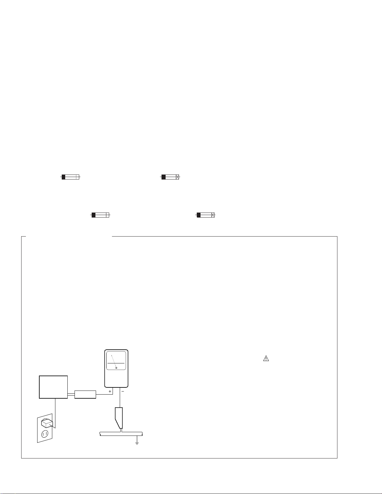
LEAKAGE CURRENT CHECK
Measure leakage current to a known earth ground
(water pipe, conduit, etc.) by connecting a leakage
current tester such as Simpson Model 229-2 or
equivalent between the earth ground and all exposed
metal parts of the appliance (input/output terminals,
screwheads, metal overlays, control shaft, etc.). Plug
the AC line cord of the appliance directly into a 120V
AC 60 Hz outlet and turn the AC power switch on. Any
current measured must not exceed 0.5 mA.
Reading should
not be above
0.5 mA
Earth ground
Device
under
test
Also test with plug
reversed
(Using AC adapter
plug as required)
Leakage
current
tester
Test all exposed
metal surfaces
AC Leakage Test
ANY MEASUREMENTS NOT WITHIN THE LIMITS
OUTLINED ABOVE ARE INDICATIVE OF A POTENTIAL SHOCK HAZARD AND MUST BE CORRECTED BEFORE RETURNING THE APPLIANCE
TO THE CUSTOMER.
2. PRODUCT SAFETY NOTICE
Many electrical and mechanical parts in the appliance have special safety related characteristics. These
are often not evident from visual inspection nor the
protection afforded by them necessarily can be obtained by using replacement components rated for
voltage, wattage , etc. Replacement parts which have
these special safety characteristics are identified in
this Service Manual.
Electrical components having such features are
identified by marking with a
on the parts list in this Service Manual.
The use of a substitute replacement component which
does not have the same safety characteristics as the
PIONEER recommended replacement one, shown in
the parts list in this Service Manual, may create shock,
fire, or other hazards.
Product Safety is continuously under review and
new instructions are issued from time to time. For
the latest information, always consult the current
PIONEER Service Manual. A subscription to, or additional copies of, PIONEER Service Manual may be
obtained at a nominal charge from PIONEER.
on the schematics and
2
Page 3
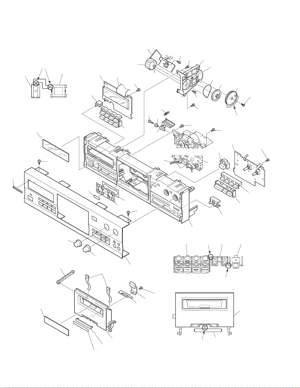
2. EXPLODED VIEWS AND PARTS LIST
NOTES : Parts marked by “ NSP ” are generally unavailable because they are not in our Master Spare Parts List.
The mark found on some component parts indicates the importance of the safety factor of the part.
Therefore, when replacing, be sure to use parts of identical designation.
Screw adjacent to mark on the product are used for disassembly.
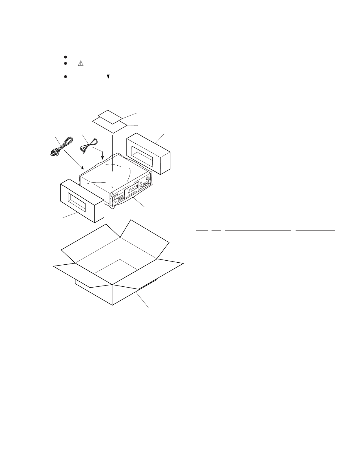
2.1 PACKING
8
CT-S670D
6
1
5
7
4
2
PACKING PARTS LIST
Mark No. Description Part No.
1 Pad (L) RHA1213
2 Pad (R) RHA1212
3 Packing Case RHG1871
4 Sheet (750 × 600 × 0.5) Z23-007
5 CD • DECK SYNCHRO Control RDE1044
Code
6 Connection Code with Pin Plugs RDE1036
(Audio Cord: L= 1.0 m)
7 Operating Instructions RRE1161
(English/French/German/Italian/
Dutch/Swedish/Spanish/
3
NSP 8 Warranty Card ARY7009
Portuguese)
3
Page 4
CT-S670D
2.2 EXTERIOR
15
20
20
20
5
3
20
19
19
27
23
21
26
12
A
22
20
21
6
10
4
13
2
21
21
22
24
9
To Mechanism
Unit
21
21
1
28
9
19
8
7
Refer to " 2.3 FRONT PANEL SECTION".
29
11
19
16
29
11
19
A
4
Page 5

EXTERIOR PARTS LIST
Mark No. Description Part No.
CT-S670D
NSP 2 TRN 2 UNIT RWZ4281
NSP 7 Main Chassis RNB1132
NSP 9 PCB Spacer PNY–404
NSP 10 FL Spacer PEB1033
NSP 12 TRANS 1 PCB RNZ3294
NSP 13 PCB Holder AEC–703
NSP 23 Binder ZCA–T18S
NSP 24 Spacer REC1319
NSP 25 …………………
1 MAIN UNIT RWZ4279
3 Strain Relief CM–22B
4 Fuse (FU801: T1.25A) AEK1055
5 AC Power Cord PDG1058
6 Power Transformer RTT1345
(AC220–230V)
8 Rear Panel RNA2199
11 Insulator PNW2766
14 …………………
15 Bonnet REA1276
16 Disc Guard REC1305
17 …………………
18 …………………
19 Screw BBZ30P080FCC
20 Screw BBZ30P080FZK
21 Screw BBZ30P060FCC
22 Screw IBZ30P150FCC
NSP 26 PWSW UNIT RWZ4280
27 Power Button RAC2193
NSP 28 FL Spacer PEB1137
29 Screw BBT30P080FCC
5
Page 6
CT-S670D
2.3 FRONT PANEL SECTION
Cut
33
No. 33 Cut Part
21
26
Not used
33
24
15
39
A
5
1
3
44
19 (1/3)
7
18
43
32
11
Refer to
" 2.4 MECHANISM UNIT ".
38
45
37
31
17
45
13
A
4
Froil PN397
6
8
31
19 (3/3)
10
16
Froil PN397
2
44
25
12
42
27
42
35
29
34
9
22
41
24
30
31
14
19 (1/3)
No. 19 Cut Part
Cut
19 (2/3)
19 (2/3)
Cut
20
19 (3/3)
23 (1/2)
Cut
23 (2/2)
28
23(2/2)
23(1/2)
No. 23 Cut Part
6
Page 7

FRONT PANEL SECTION PARTS LIST
Mark No. Description Part No.
1 FL UNIT RWX1146
2 OPSW UNIT RWX1142
3 FFC 33P (60V) RDD1400
4 Mechanism Unit RYM1271
5 DC Motor/0.75W PXM1010
6 Rubber Belt PEB1127
7 Motor Pulley PNW1634
8 Pulley Gear RNK1517
9 Spring RBK1004
10 Arm Gear RNK2304
11 SW Lever RNK1897
12 Joint Arm RNK2243
13 Loading Base Assy 2 RXA1750
14 Panel Stay RNT1247
NSP 15 POCM UNIT RWZ4282
CT-S670D
16 Screw IPZ20P080FMC
17 Screw BMZ26P040FMC
18 Spring RBH1008
19 Function Button B RAC2191
20 Play Button B RAC2204
21 FL Lens RAH2846
22 Front Panel RAH2848
23 Door Pocket RAH2843
24 Screw BBT30P080FCC
25 Door Lens RAH2782
26 Name Plate AAM7004
27 Indicating Panel REE–113
28 Door Plate RAH2850
29 Stabilizer B REB1085
30 Digi Lens RAC2200
31 Screw BBZ30P060FCC
32 Eject Collar RLA1303
33 Slide Knob RAC2203
34 Stabilizer Panel RAH1483
35 Manual Button RAC2195
36 …………………
37 Connector Assy 3P RKP1673
38 Connector Assy 2P RKP1681
39 Screw BBZ26P060FMC
40 …………………
NSP 41 LED UNIT RWX1143
42 VOL Knob RAC2197
43 Screw BBZ26P100FMC
44 Screw BBZ30P080FZK
45 Screw BBZ30P100FMC
7
Page 8
CT-S670D
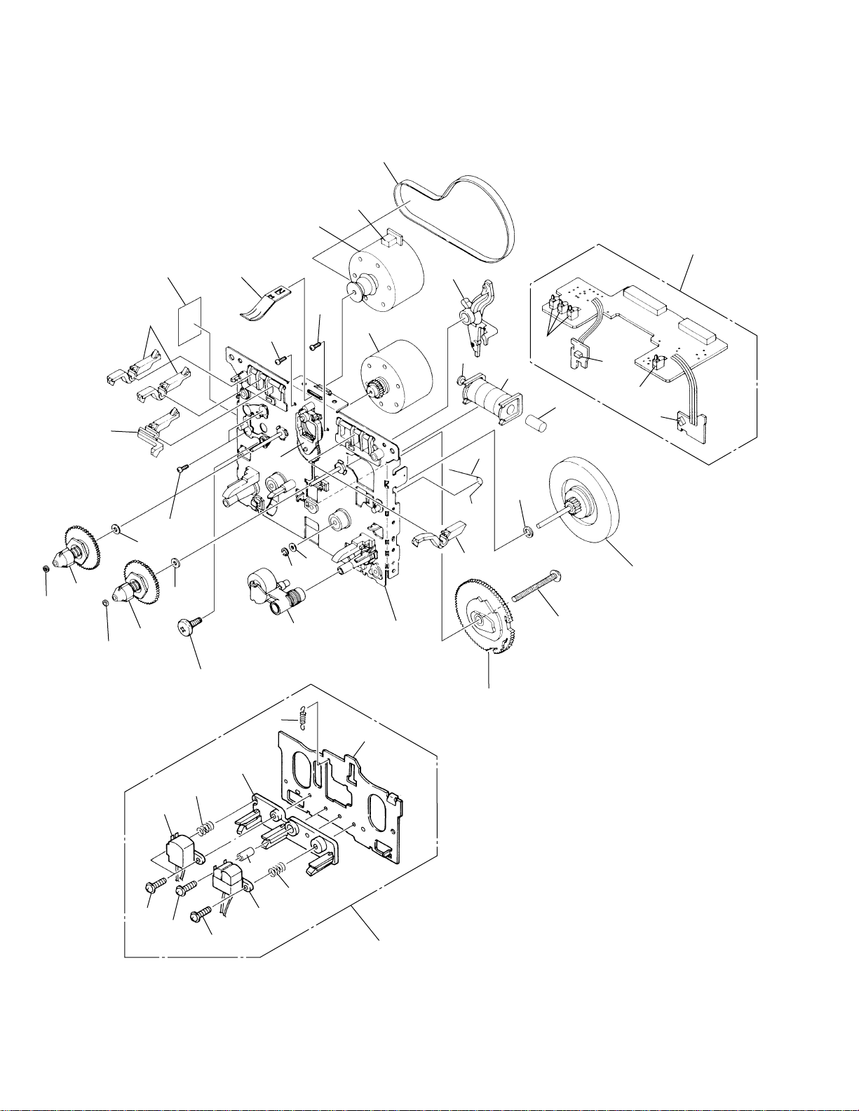
2.4 MECHANISM UNIT SECTION
7
26
28
10
42
45
23
15
16
31
15
16
19
30
36
19
38
14
17
41
11
40
14
6
2
22
32
29
24
5
8
1
13
44
This screw No. 44 is the part to hold the
cam gear for servicing, when the hook
holding the cam gear No. 24 is broken.
9
5
9
12
21
27
33
20
4
39
20
37
34
43
3
35
8
Page 9

MECHANISM UNIT SECTION PARTS LIST
Mark No. Description Part No.
1 FIXED CORE RLA1130
2 PLUNGER RLA1132
3 HEAD (R/P) RPB1047
4 HEAD (E) RPB1060
5 PUSH SW RSG1018
6 MTR REEL BLK RXM1057
7 MTR MAIN BLK RXM1058
8 SOLENOID BLK RXP1010
9 PHOTO-TRANSISTOR SPI33534FG
10 MAIN BELT REB1163
11 PINCH ROLLER ASSY RXA1183
12 FLYWHEEL ASSY RXA1772
13 WASHER WA26D045D025
14 SCREW 2.6 × 6.4 ZN RBA1076
15 WASHER RBF–057
16 REEL BASE BLK RXA1184
17 IDLER BLK RXA1248
18 …………………
19 WASHER 2.1 × 0.25T RBF1038
20 AZIMUTH SPRING RBH1076
CT-S670D
21 HAED BASE SPRING RBL1003
22 SLIDE SPRING RBH1239
23 PLAY ARM RNK1525
24 CAM GEAR (3R) RNK1672
25 …………………
NSP 26 SPACER REC1319
27 HEAD BASE RNE1390
28 SPRING CASSETTE RBK1048
29 CHASSIS BASE BLK RXA1557
30 DETECTOR LEVER (REC) RNK1527
31 METAL DETECTOR LEVER (L) RNK1529
32 DETECTOR LEVER (P) RNK1543
33 HEAD SPACER RNK2106
34 SCREW PMZ20P080FMC
35 PLATE HD BLK RXA1488
36 SCREW PMA26P050FMC
37 F LOOK SCREW M2 × 10 RBH1031
38 SCREW RBA1101
39 SPACER RLA1275
40 WASHER WA26D047D050
41 WASHER YE15FUC
42 HOLDER CUSHION (L) RED1027
43 F LOOK SCREW 2 × 8 RBA1102
44 SCREW TT2 × 15 RBA1068
45 PCB CONTROL BLK RXA1771
9
Page 10
1
234
CT-S670D
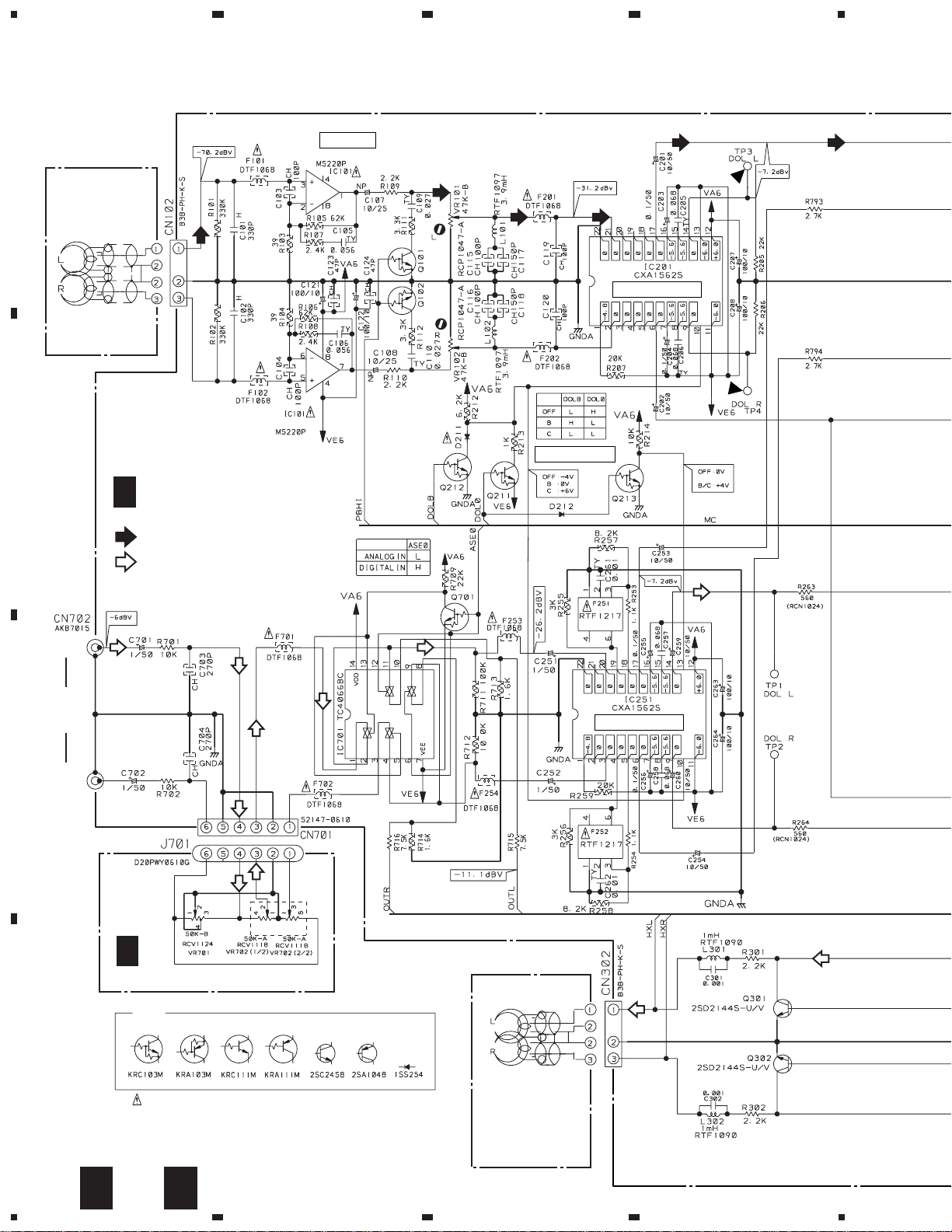
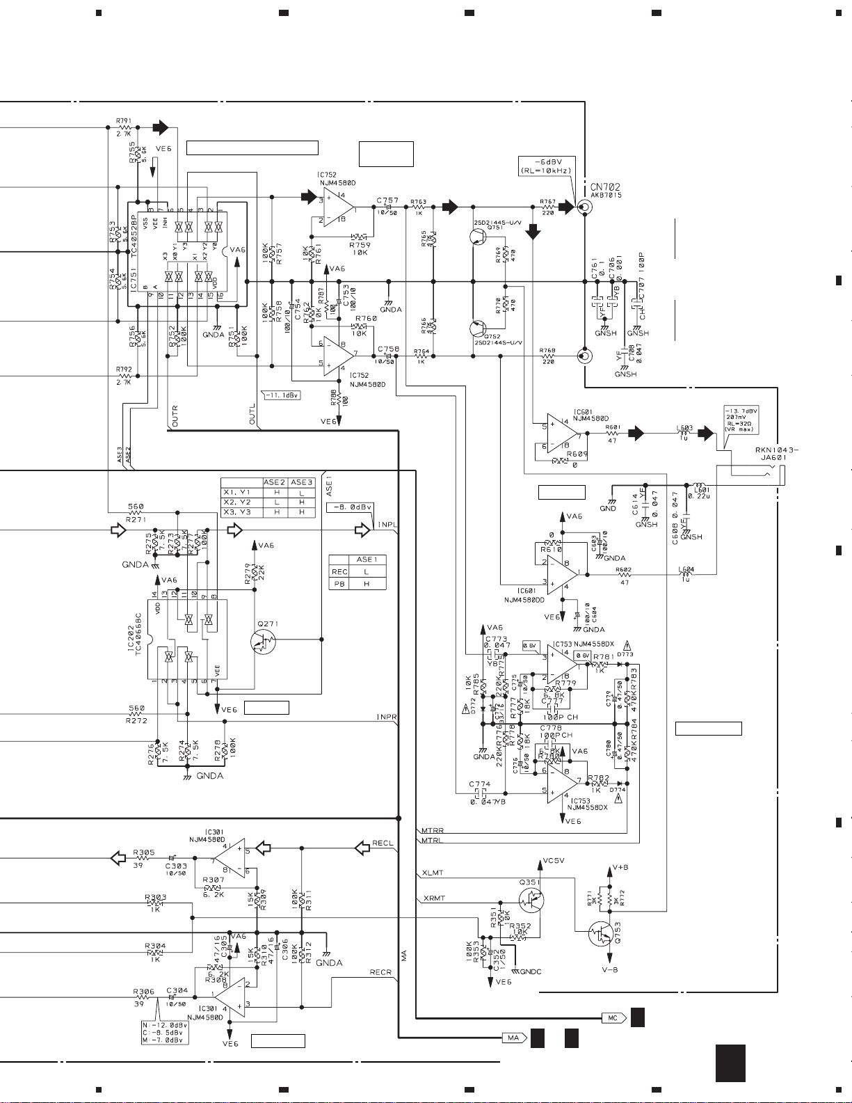
3. SCHEMATIC DIAGRAM
3.1 OVERALL SCHEMATIC DIAGRAM
A
Note: When ordering service parts, be sure to refer to "EXPLODED
VIEWS and PARTS LIST" or "PCB PARTS LIST".
CN702 (3/4)
AKB7015
CN702 (4/4)
AKB7015
MECHA UNIT
(RYM1271)
B3B-PH-K-S
P.B
HEAD
B
REC
HEAD
ERASE
HEAD
CN81
RECINH
HARF
B3B-PH-K-S
D20PYY0710G
POCM UNIT
G
(RWZ4282)
(
A
D20PWY0510G
A
1/4 to A 4/4
)
LED UNIT
F
(RWX1143)
PG02MR-F30
173981-2
MAIN UNIT
CrO2
(RWZ4279)
METAL
CN82
C
R.M
C.M
D
D20PYY1010G
FL UNIT
E
(RWX1146)
10
1234
Page 11
5
67
8
CT-S670D
B
OPSW UNIT
(RWX1142)
D20PWY0310G
(
B
1/2, B 2/2
A
)
(
A
1/4 to A 4/4
MAIN UNIT
(RWZ4279)
D20PWY0610G
52147-0610
)
CN702 (1/4)
AKB7015
CN702 (2/4)
AKB7015
JA911
JA912
JA1801
GPIF32R
A
B
DXWW0315E
TRN 2 UNIT
D
(RWZ4281)
FU801
T1.25AL250V
H1, H2:
AKR7001
POWER
TRANSFORMER
RTT1345
C
PWSW UNIT
(RWZ4280)
TRNS 1 PCB
(RNZ3294)
CN1001
JA901
JA601
AC POWER CORD
PDG1058
NEUTRAL
LIVE
AC220–230V
50/60Hz
C
D
D20PWW0615G
11
5
6
7
8
Page 12
1
234
CT-S670D
3.2 MAIN UNIT (1/4) AND OPSW UNIT (1/2)
A
MECHA UNIT
(1/4)
(RYM1271)
B
P. B HEAD
RPB1047 (1/2)
A
MAIN UNIT (1/4)
1/4
(RWZ4279)
: PLAYBACK SIGNAL ROUTE
: RECORDING SIGNAL ROUTE
PB AMP
PB LEVEL
ADJ.
BIAS
TRAP
DOLBY B/C NR
DOLBY CONT
C
D
Lch
LINE
INPUT
Rch
B
1/2
OPSW UNIT (RWX1142)
NOTE
If the parts are not identified in the diagram the followings are used.
The mark found on some component parts indicates the importance of the
safety factor of the part. Therefore, when replacing, be sure to use parts of
identical designation.
REC HEAD
RPB1047 (2/2)
MECHA UNIT
(2/4)
(RYM1271)
DOLBY B/C NR
12
A 1/4 B 1/2
1234
Page 13
5
67
8
CT-S670D
TAPE/SOURCE/REC MONI
LINE OUT
BUFFER
A
Lch
LINE
OUT
Rch
B
HP AMP
C
PB/REC
METER AMP
D
A
2/4
REC AMP
5
6
A
2/4
A
3/4
7
8
A 1/4
13
Page 14

1
CT-S670D
3.3 MAIN UNIT (2/4)
234
A
B
A
MAIN UNIT (2/4)
2/4
(RWZ4279)
DSP
A
1/4
C
LRCK, BCLK (FROM DIR)
ON/OFF
NOTE
If the parts are not identified in the diagram the followings are used.
D
14
A 2/4
The mark found on some component parts indicates the importance of the
safety factor of the part. Therefore, when replacing, be sure to use parts of
identical designation.
1234
Page 15

5
67
8
CT-S670D
A
RAM
X'TAL/VCO
X1731:
18.432 MHz
X'TAL
A
B
3/4
C
DIR
D
5
6
7
8
A 2/4
15
Page 16

1
234
CT-S670D
3.4 MAIN UNIT(3/4), PWSW UNIT AND TRN2 UNIT
A
B
A
MAIN UNIT (3/4)
3/4
(RWZ4279)
S5688G
S5688G
S5688G
S5688G
C1025C1026
CAUTION: FOR CONTINUED PROTECTION AGAINST RISK OF FIRE.
REPLACE ONLY WITH SAME TIME NO. ICP-N15, MFD BY
ROHM CO., LTD. FOR IC1003 and IC1004.
HEAT SINK
POWER SUPPLY
10/50
1000/16
10/50
470/25
EARTH METAL
FITTING
470/25
POWER OFF
C
C
TRN1 PCB
(RNZ3294)
FU801
AKR7001
D
TRN2 UNIT
D
(RWZ4281)
16
A 3/4
1234
C D
T1.25AL250V
NOTE FOR FUSE REPLACEMENT
CAUTION: FOR CONTINUED PROTECTION AGAINST RISK OF FIRE.
REPLACE ONLY WITH SAME TIME AND RATINGS ONLY.
PWSW UNIT
(RWZ4280)
AC POWER CORD
PDG1058
AC220–230V
50/60 Hz
Page 17

A
2/4
5
67
8
CT-S670D
MECHA UNIT (3/4)
(RYM1271)
A
A
1/4
BIAS OSC
160 kHz
HX PRO
(RPB1060)
B
BLEXD
CONT
BIAS CONTROL
D/A CONVERTER
NOTE
If the parts are not identified in the diagram the followings are used.
A
4/4
C
D
The mark found on some component parts indicates the importance of the
safety factor of the part. Therefore, when replacing, be sure to use parts of
identical designation.
5
6
7
8
A 3/4
17
Page 18

1
234
CT-S670D
3.5 MAIN UNIT (4/4), OPSW UNIT (2/2), FL UNIT, LED UNIT AND POCM UNIT
MAIN UNIT (4/4)
4/4
(RWZ4279)
NOTE
If the parts are not identified in the diagram the followings are used.
The mark found on some component parts indicates the importance of the
safety factor of the part. Therefore, when replacing, be sure to use parts of
identical designation.
MEMORY
MC
A
A
3/4
A
B
FL HOLDER
C
E
FL UNIT (RWX1146)
SWITCHES:
FL UNIT
S1503: COUNTER RESET
S1504: FLEX
S1505: METER RANGE/DISO OFF
S1506: COUNTER MODE
S1507: DIGITAL- NR
S1508: DOLBY NR
S1509: DIGITAL IN
S1510: MONITER
OPSW UNIT
S1601:
S1602: EJECT
S1603: REC
S1604: PAUSE
S1605: CD SYNC
D
S1607: MUTE
S1608: PLAY
S1609: F F
S1610: REW
S1611: BLE XD
STOP
B
2/2
OPSW UNIT
(RWX1142)
18
A 4/4 B 2/2
1234
E
Page 19

5
67
8
CT-S670D
MC
MECHA CONTROL
A
G
POCM UNIT
(RWZ4282)
B
HOLDERHOLDER
µ-COM
MECHA UNIT (4/4)
(RYM1271)
C
D
LED UNIT
F
(RWX1143)
5
6
7
A 4/4
F
G
8
19
Page 20

1
234
CT-S670D
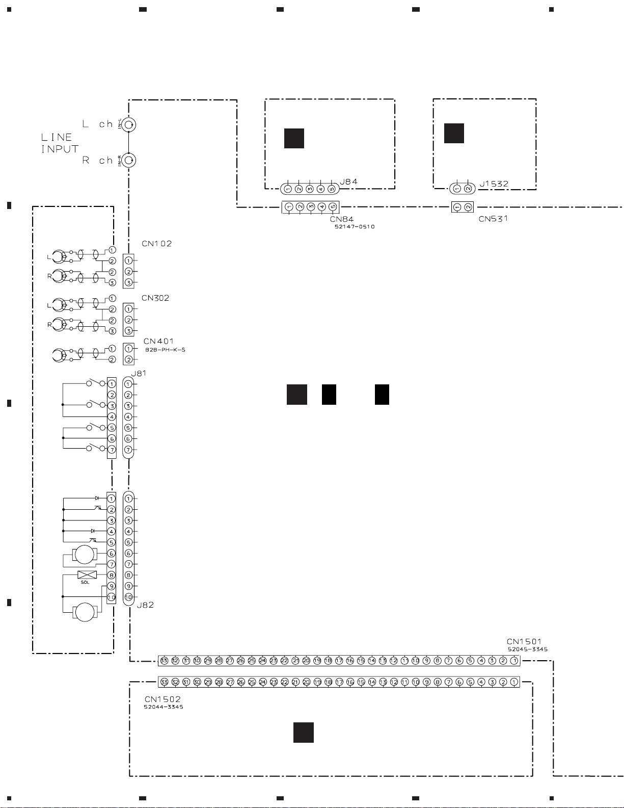
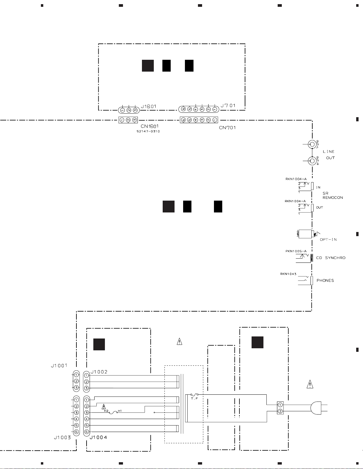
4. PCB CONNECTION DIAGRAM
A
B
NOTE FOR PCB DIAGRAMS:
1. Part numbers in PCB diagrams match those in the schematic
diagrams.
2. A comparison between the main parts of PCB and schematic
diagrams is shown below.
Symbol in PCB
Diagrams
BCE
BCE
DGS
Symbol in Schematic
Diagrams
BCE
BCEBCE
DGSDGS
BCE
4.1 LED UNIT AND POCM UNIT
Part Name
Transistor
Transistor
with resistor
Field effect
transistor
Symbol in PCB
Diagrams
3. The parts mounted on this PCB include all necessary parts
for several destination.
For further information for respective destinations, be sure
to check with the schematic diagram.
4. Viewpoint of PCB diagrams
Symbol in Schematic
Diagrams
CapacitorConnector
Part Name
Resistor array
3-terminal
regulator
SIDE A
P. C. Board Chip Part
SIDE B
SIDE A
LED UNIT
F
RNP1724–A
C
POCM UNIT
G
D
A
CN531
A
CN84
RNP1725–A
20
F
G
1234
Page 21

1
23
4.2 PWSW UNIT, TRN2 UNIT AND TRN1 PCB
D
TRN2 UNIT
4
CT-S670D
A
SIDE A
A
J1001
A
J1003
TRN1 PCB
POWER TRANSFORMER
B
AC POWER CORD
1
NEUTRAL
LIVE
C
PWSW UNIT
2
C
PNP1725–A
D
3
C
D
4
21
Page 22

1
CT-S670D
234
4.3 MAIN UNIT
IC1012
IC1013
IC1011
Q1001
Q1003
IC1003
IC1001
Q1002
Q1004
IC1004
Q753
Q351
IC1821
A
B
D
J1002
D
J1004
E
CN1502
A
MAIN UNIT
Q531
IC1014
Q1731
Q1005
Q572
Q571
IC591
IC801
C
Q801
|
Q807
MECHA UNIT
CN82
MECHA UNIT
CN81
RNP1725–A
F
J1532
G
J84
D
22
A
1234
Page 23

5
67
8
CT-S670D
SIDE A
A
Q751
Q752
Q902
IC753
IC752
IC301
VR102
IC202
VR101
MECHA UNIT
PB HEAD
Q271
Q401
|
Q403
Q301
Q302
IC601
IC751
Q102
IC201
IC101
Q101
IC251
IC701
B
C
MECHA
UNIT
ERACE HEAD
MECHA
UNIT
REC HEAD
Q701
Q211
|
IC451
Q213
B
J701
B
J1601
VR601
A
5
6
7
8
23
D
Page 24

CT-S670D
A
IC1801
IC1751
1
A
MAIN UNIT
234
B
C
IC1701
D
24
A
1234
Page 25

5
67
8
CT-S670D
SIDE B
IC1802
A
IC1761
B
IC1741
IC1851
IC1731
IC501
IC551
C
RNP1725–A
D
5
6
7
8
A
25
Page 26

1
CT-S670D
234
4.4 OPSW UNIT AND FL UNIT
A
B
OPSW UNIT
B
A
CN1601
SIDE A
A
CN701
E
FL UNIT
C
D
RNP1724–A
A
CN1501
26
B
E
1234
Page 27

5. PCB PARTS LIST
NOTES :
Parts marked by “ NSP ” are generally unavailable because they are not in our Master Spare Parts List.
The mark found on some component parts indicates the importance of the safety factor of the part.
Therefore, when replacing, be sure to use parts of identical designation.
When ordering resistors, first convert resistance values into code form as shown in the following examples.
Ex. 1 When there are 2 effective digits (any digit apart from 0), such as 560 ohm and 47k ohm (tolerance is shown by
J = 5%, and K = 10%).
1
560 Ω = 56 × 10
47k Ω = 47 × 10
= 561................................................... RD1/4PU 5 6 1 J
3
= 473 .................................................. RD1/4PU 4 7 3 J
0.5 Ω = R50 ...................................................................... RN2H Â 5 0 K
1 Ω = 1R0 ......................................................................... RS1P 1 Â 0 K
Ex. 2 When there are 3 effective digits (such as in high precision metal film resistors).
5.62k Ω = 562 × 10
1
CT-S670D
= 5621 ........................................... RN1/4PC 5 6 2 1 F
Mark No. Description Part No.
LIST OF PCB ASSEMBLIES
NSP MOTHER UNIT RWM2045
NSP PWSW UNIT RWZ4280
NSP TRN 2 UNIT RWZ4281
NSP POCM UNIT RWZ4282
NSP SUB UNIT RWM2049
NSP LED UNIT RWX1143
A
MAIN UNIT RWZ4279
FL UNIT RWX1146
OPSW UNIT RWX1142
MAIN UNIT
SEMICONDUCTORS
IC1701 AK7712A-VQ
IC591 AT24C01-10PC
IC201, IC251 CXA1562S
IC1003, IC1004 ICP-N15
IC1001 M5218AP
IC101 M5220P
IC1751 M5M51008BFP-70L
IC551 M62354GP
IC753 NJM4558DX
IC301, IC601, IC752 NJM4580D
IC1011, IC1012 NJM7805FA
IC1821 PD0052
IC501 PD5431A
IC1013 PQ12RF11
IC1014 S-806D
IC801 TA7288P
IC751 TC4052BP
IC202, IC701 TC4066BP
IC1741 TC74HC00AF
IC1851 TC74HC125AF
IC1761 TC7S08F
IC1731 TC7SU04F
IC451 UPC1297CA
Q1002, Q1005 2SA1048
Q1004 2SB1566
Mark No. Description Part No.
Q401, Q402 2SC1815
Q1001, Q571, Q572, Q802, Q806 2SC2458
Q805 2SC3246
Q803, Q804 2SD1858X
Q301, Q302, Q403, Q751, Q752 2SD2144S
Q1003 2SD2395
Q351 KRA103M
Q101, Q102, Q1731, Q211–Q213 KRC103M
Q271, Q531, Q701, Q753, Q801 KRC103M
Q807, Q902 KRC103M
D1021, D1022 1SS254
D1023 1SS254
D211, D212, D402 1SS254
D772–D774, D820–D827 1SS254
D901–D903, D908–D910 1SS254
D1731–D1733, D1821 1SS355
D1005, D1006 HZS6C1L
D1020 MTZJ6.2B
D1011 S2VB20
D1001–D1004, D1015, D1016 S5688G
D1019 S5688G
D801 S5688G
COILS AND FILTERS
F101, F102, F201, F202 DTF1068
F253, F254, F701, F702 DTF1068
L603, L604 LAU1R0J
L901, L902 LAU1R0K
L904 LAU4R7J
L601 LAUR22J
L402 LFA121K
L1801 LFA151K
L1701, L1702, L1731, L1741, L1751 LFA1R0K
L1821, L1822, L1851 LFA1R0K
X501 (8.389 MHz) RSS1042
X1731 (18.432 MHz) RSS1052
L451, L452 (160 kHz) RTD1074
L401 (OSC COIL F=160 kHz) RTD1076
L301, L302 (1 mH) RTF1090
L101, L102 (3.9 mH) RTF1097
L1802 (EMI FILTER) RTF1171
F251, F252 (MPX FILTER) RTF1217
27
Page 28

CT-S670D
Mark No. Description Part No. Mark No. Description Part No.
CAPACITORS
C459, C460 CCCSL271K2H
C1834 CCSQCH100D50
C103, C104, C115, C116 CCSQCH101J50
C119, C120, C463, C707 CCSQCH101J50
C777, C778 CCSQCH101J50
C117, C118 CCSQCH151J50
C1734, C1735 CCSQCH180J50
C1823 CCSQCH220J50
C703, C704, C905 CCSQCH271J50
C123, C124, C805, C807 CCSQCH470J50
C1020, C1742, C1751, C1761 CEAT100M50
C775, C776, C803 CEAT100M50
C1017, C121, C122, C207, C208 CEAT101M10
C263, C264, C603, C604 CEAT101M10
C1016 CEAT101M16
C1019 CEAT101M50
C352 CEAT1R0M50
C1825 CEAT2R2M50
C407, C465, C772 CEAT330M16
C1721, C1722, C1732, C1802, C1804 CEAT470M16
C1821, C1838, C1851, C305, C306 CEAT470M16
C406, C501 CEAT470M16
C1015 CEAT472M25
C203, C204, C255, C256 CEATR10M50
C779, C780 CEATR47M50
C1762, C1801, C1822, C1839, C761 CKSQYF104Z25
C1712, C1805, C1833, C801, C802 CKSQYF473Z50
C906 CKSQYF473Z50
C101, C102 CQHA331J2A
C402 CQHA392J2A
C301, C302 CQMA102J50
C405 CQMA123J50
C401, C404 CQMA332J50
C1824 CQMA473J50
C403 CQMA682J50
C1014 (1000 µF/16V) PCH1122
C461, C462 (470 pF/500V) RCG1006
C753, C754 (100 µF/10V) RCH1133
C1706, C1708, C1711, C1716 VCH1083
(22 µF/25V)
RESISTORS
R525 RA4T103J
R205, R206 RCN1023
R263, R264 RCN1024
R402 RD1/2LMF1R0J
R408 RD1/2VM330J
R403, R404 RD1/2VM4R7J
R787, R788 RD1/4PU101J
R1005, R1006, R763, R764 RD1/4PU102J
R519, R701, R702 RD1/4PU103J
R253, R254 RD1/4PU112J
C1005, C1006, C1719, C1720 CEBA100M50
C201, C202, C253, C254 CEBA100M50
C259, C260, C303, C304 CEBA100M50
C757, C758 CEBA100M50
C1725–C1728, C251, C252 CEBA1R0M50
C701, C702 CEBA1R0M50
C1025, C1026 CEBA222M16
C1009, C1010 CEBA471M25
C107, C108 CEYANP100M25
C261, C262, C451, C452 CFTYA103J50
C455, C456 CFTYA223J50
C109, C110 CFTYA273J50
C1007, C1008, C105, C106 CFTYA563J50
C205, C206, C257, C258 CFTYA683J50
C1815 CGCYF104Z25
C505 CKCYF103Z50
C1001, C1002, C1011, C1012, C1021 CKCYF473Z50
C1024, C608, C614, C708 CKCYF473Z50
C706 CKSQYB102K50
C1713, C1733, C1736, C1852 CKSQYB103K50
C502–C504, C552, C591, C804 CKSQYB103K50
C806, C901, C902 CKSQYB103K50
C457, C458 CKSQYB123K50
C555, C556 CKSQYB221K50
C1831, C1832, CKSQYB223K50
C1723, C1724 CKSQYB332K50
C773, C774 CKSQYB473K50
C453, C454 CKSQYB821K50
C1701–C1705, C1707, C1709, C1710 CKSQYF104Z25
C1714, C1715, C1731, C1741, C1752 CKSQYF104Z25
R401, R406 RD1/4PU123J
R1001, R1002 RD1/4PU151J
R805, R808, R814 RD1/4PU152J
R577, R578 RD1/4PU202J
R767, R768 RD1/4PU221J
R109, R110, R301, R302 RD1/4PU222J
R812, R813 RD1/4PU223J
R791–R794, R804 RD1/4PU272J
R1727, R1728, R531 RD1/4PU301J
R771, R772 RD1/4PU302J
R806 RD1/4PU332J
R305, R306 RD1/4PU390J
R1003, R1004, R601, R602 RD1/4PU470J
R271, R272 RD1/4PU561J
R1015 RD1/4PU562J
R715, R716 RD1/4PU752J
R1017 RFA1/4PL820J
VR101, VR102 (47 kΩ) RCP1047
R807 RS2LMF560J
Other Resistors RS1/10S J
OTHERS
CN531 MT CONNECTOR 2P 173981-2
CN701 6P JUMPER CONNECTOR 52147-0610
CN84 5P JUMPER CONNECTOR 52147-0510
CN1601 3P JUMPER CONNECTOR 52147-0310
CN1501 33P FFC CONNECTOR 52045-3345
CN401 KR CONNECTOR 2P B2B-PH-K-S
JA1801 OPTICAL LINK IN GP1F32R
CN702 4P PIN JACK AKB7015
JA601 HEADPHONE JACK RKN1043
J81 2m/m PITCH WIRE 7P D20PYY0710G
28
Page 29

CT-S670D
Mark No. Description Part No. Mark No. Description Part No.
JA911, JA912 REMOTO JACK RKN1004
CN102, CN302 SP CONNECTOR B3B-PH-K-S
JA901 MINI JACK PKN1005
J1003 2m/m PITCH WIRE 6P D20PWW0615G
J1001 PARALLEL CORD DXWW0315E
LED UNIT
F
SEMICONDUCTORS
D1531–D1533 (PURE GREEN ) MBG5074X
J82 2m/m JUMPER WIRE 10P D20PYY1010G
PWSW UNIT
C
SWITCH
S991 RSA1001
CAPACITOR
C991 (10000pF/250V) ACG7020
OTHERS
FL UNIT
E
SEMICONDUCTORS
D1501–D1503 1SS254
SWITCHES
S1501 ( SLIDE SW ) RSH1041
S1503–S1510 VSG1009
GROUND PLATE VNF-091
PCB BINDER VEF1040
7P CABLE HOLDER 51048-0700
10P CABLE HOLDER 51048-1000
TERMINAL RKC-061
PCB BINDER VEF1040
OTHER
J1532 CONNECTOR ASSY PG02MR-F30
TRN 2 UNIT
D
OTHERS
H1, H2 FUSE CLIP AKR7001
G
POCM UNIT
OTHERS
J84 2m/m PITCH WIRE D20PWY0510G
REAF SW VSK1011
RESISTORS
All Resistors RD1/4PU J
OTHERS
CN1502 33P FFC CONNECTOR 52044-3345
V1501 FL TUBE RAW1163
OPSW UNIT
B
SWITCHES
S1601–S1605, S1607–S1611 VSG1009
RESISTORS
VR702 (50 kΩ–A) RCV1118
VR701 (50 kΩ–B) RCV1124
Other Resistors RD1/4PU J
OTHERS
J1601 3P JUMPER WIRE D20PWY0310G
J701 2m/m JUMPER WIRE D20PWY0610G
29
Page 30

CT-S670D
6. ADJUSTMENT
Adjustment points and Measurement points are shown in Fig. 6–5.
6.1 MECHANICAL ADJUSTMENT
Tape Speed Adjustment
Mode Test Tape Adjusting Point
PLAY NCT-111 (3kHz) Capstan Motor 3000Hz ± 5Hz
Specifications/Ratings
(Playback Frequency)
Note) Always use a ceramic screwdriver
for adjustment.
6.2 ELECTRICAL ADJUSTMENT
Adjustment Conditions
(1) The mechanical adjustments must be completed first.
(2) The head must be cleaned and demagnetized.
(3) Turn the power on allow the deck to warm up for at least a few
minutes before commencing any electrical adjustments.
(4) The reference signal is 0 dBV = 1 Vrms.
(5) Connect a10 kΩ load resistance to the OUTPUT terminals.
(6) Unless otherwise specified, the switches listed below are left in
the positions indicated.
DOLBY NR : OFF
DIGITAL NR : OFF
List of Adjustments
Playback Section
(1) Head Azimuth Adjustment
(2) Playback Level Adjustment
Recording Section
(1) Bias Oscillator Adjustment
(2) Recording Bias and Recording Level Automatic Adjustment
NOTE: This unit has an automatic tape selection feature.
Remarks
Test Tape
STD–331E : Playback adjustment (See Fig. 6–1)
STD–632 : NORMAL blank tape
STD–622 : CrO2 blank tape
STD–611 : METAL blank tape
∗As the reference recording level is 250 nwb/m for STD–331E,
the recording level will be higher by 4 dB for STD–331B
(160nwb/m). When adjusting, pay careful attention to the type
of tape used.
0 dB
30
30s
315 Hz
0 dB: 315 Hz, 250 nwb/m
30 s 30 s 30 s 10s 10s ................................................................................................................ 10s
6.3 kHz 10 kHz 315 Hz 14 kHz
12.5
kHz
Fig. 6–1 Constants of the Test Tape STD–331E
Dolby noise reduction and HX Pro headroom extension manufactured
under license from Dolby Laboratories Licensing Corporation. HX Pro
originated by Bang & Olufsen.
“DOLBY”, the double-D symbol and “HX PRO” are trademarks of Dolby
Laboratories Licensing Corporation.
10 kHz
8 kHz 4 kHz 2 kHz
6.3
kHz
1 kHz
500Hz250Hz125
Hz
63 Hz 40 Hz
–20 dB
Page 31

CT-S670D
PLAY BACK
250
3dB
10k
3dB
Fig. 6–2 Frequency Response Zone
6.2.1 Playback Section
(1) Head Azimuth Adjustment
Turn VR101 and VR102 to mechanical center position.
No. Mode Input Signal / Test Tape
1
PLAY
Play the 10 kHz/–20 dB section
of STD–331E test tape
adjustment screw
RECORDING
12.5k
4dB
315 Hz = 0 dB 315 Hz = 0 dB
250
3dB
Adjustment Measurement Adjustment
Location Location Value
Head azimuth
(Fig. 6–3)
LINE OUT
(L/R ch)
Maximum playback
signal level
10k
3dB 5dB
12.5k
Lock the screw with silicon
bond after completing
adjustment.
Remarks
Fig. 6–3 Head Azimuth Adjustment
(2) Playback Level Adjustment
This adjustment determines the DOLBY NR level, and must be performed with great care.
No. Mode Input Signal / Test Tape
1
PLAY
Play the 315 Hz/ 0 dB section of
STD–331E test tape
Adjustment Measurement Adjustment
Location Location Value
VR101L ch
R ch VR102
TP3 (L ch)
TP4 (R ch)
(MAIN Unit)
6.2.2 Recording Section
(1) Bias Oscillation Frequency Adjustment
No. Mode Input Signal / Test Tape
1 TP11
REC
Load the STD–611 test tape with
no input signal.
Adjustment Measurement Adjustment
Location Location Value
L401
Head Azimuth Adjustment Screw
Remarks
–6.7 dBV
Remarks
160 kHz ± 1 kHz
31
Page 32

CT-S670D
(2) Recording Bias and Recording Level Automatic Adjustment
1 Press the MODE key, RESET key and the PAUSE key together to enter the into test mode.
‘
2 Press the MODE key, PAUSE key and the MUTE key together to clear all memory data. At this time, “CLR” is displayed on the
counter.
‘
3 Press the STOP key to set the level (MS) display to “10” (mechanism operation check mode).
‘
4 Press the XD FLAT key to set the level (MS) display to “80” (automatic adjustment mode).
‘
5 When the test tape (STD–632) is inserted and the REC key is pressed, “B” flashes on the counter and bias adjustment is started. When
adjustment is completed correctly, “B” will light steadily, and then “R” will flash and adjustment of the recording level will start. When
the adjustment is completed correctly, “BR” will light to indicate that the adjustment has been completed correctly. When at the time
“B” lights, this indicates a bias adjustment error, and when “R” lights, this indicates a recording level adjustment error. At the time
of an error, the adjustment value is not written to the memory.
Adjustment error: The following causes can be considered.
Recording is not being done.
The adjustment tape is damaged seriously.
There is no adjustment data. The tape is near the tape end.
Circuit trouble (defective contact etc.)
‘
6 When the STOP key is pressed, automatic adjustment mode is cancelled, the level (MS) display becomes “10” (mechanism operation
check mode), and “TUNE” is displayed on the counter.
‘
7 Press the RESET key to leave test mode.
Counter Display
Fig. 6–4 FL Display Position
Level (MS) Display
L401
TP11
IC202
R402
TP4
R206
TP3
R205
MAIN UNIT
IC201
IC251
IC751
VR102
IC101
VR101
IC701
32
Front
Fig. 6–5 Adjustment and Measurement Points
Page 33

7. GENERAL INFORMATION
CT-S670D
7.1 PARTS
7.1.1 IC
PD5431A (IC501: MAIN UNIT)
System Control Micro-computer
Pin Function
No. Name I/O Description
1 MTRR I Level meter R ch input
2 MTRL I Level meter L ch input
3 XNRR O NORMAL Tape Recording: “L”
4 XNRL O NORMAL Tape Recording: “L”
5 METR O METAL Tape Recording: “H”
6 METL O METAL Tape Recording: “H”
7 VCOI O DIR VCO oscillation control Stop: “H”
8 SCK O Clock output to DSP
9 SO O Data output to DSP
10 SI I Data input from DSP
¶ The information shown in the list is basic information and may
not correspond exactly to that shown in the schematic diagrams.
No. Name I/O Description
28 SOLB O Solenoid control terminal B
29 CPM O Capstan motor control terminal
30 DIG1 O Digital input select terminal 1
31 DIG2 O Digital input select terminal 2
32 SSEN I Supply side sensing input terminal
33 REMT I Remote control input terminal
34 POFF I Power off input terminal
35 REST I Reset input terminal
36 XCIN I Sub clock input terminal
37 XCOUT O Sub clock output terminal
11 RSTB O Reset output to DSP
12 PDB O Power down output to DSP
13 RQB O Request output to DSP
14 CSB O DSP chip select
15 RM2 O Motor driver control terminal 2
16 RM1 O Motor driver control terminal 1
17 RM0 O Motor driver control terminal 0
18 RMPL O Reel motor torque control terminal
19 XL3 I/O BLE · XD BIAS control terminal 3 (L ch)
20 XL2 I/O BLE · XD BIAS control terminal 2 (L ch)
21 XL1 I/O BLE · XD BIAS control terminal 1 (L ch)
22 XL0 I/O BLE · XD BIAS control terminal 0 (L ch)
23 XR3 I/O BLE · XD BIAS control terminal 3 (R ch)
24 XR2 I/O BLE · XD BIAS control terminal 2 (R ch)
25 XR1 I/O BLE · XD BIAS control terminal 1 (R ch)
38 XIN I Clock input terminal
39 XOUT O Clock output terminal
40 VSS I GND
41 X12V O VC12V control terminal “H”: 12V ON
42 TSEN I Take up side sensing input terminal
43 BIAS O Bias control terminal “H”: Bias ON
44 TOCD O CD SYNCHRO control terminal
45 SW3 Switch input terminal 3
| | I |
48 SW0 Switch input terminal 0
49 RMPS O PLAY torque SLOW terminal (Used at DTC)
50 DAT I/O EEPROM/DAC data input/output terminal
51 CLK O EEPROM/DAC clock input/output terminal
52 NC I OPEN
53 CSDA O DAC chip select terminal
54 ERR I DIR error input terminal
26 XR0 I/O BLE · XD BIAS control terminal 0 (R ch)
27 SOLA O Solenoid control terminal A
55 441k I f=44.1 input terminal
56 EMPH I Emphasis input terminal
33
Page 34

CT-S670D
PD5431A
No. Name I/O Description
57 G1 FL FL grid terminal 1
58 G2 FL FL grid terminal 2
59 G3 FL FL grid terminal 3
60 G4 FL FL grid terminal 4
61 G5 FL FL grid terminal 5
62 G6 FL FL grid terminal 6
63 G7 FL FL grid terminal 7
64 G8 FL FL grid terminal 8
65 G9 FL FL grid terminal 9
66 G10 FL FL grid terminal 10
67 P14 FL FL segment terminal 14
68 P13 FL FL segment terminal 13
69 P12 FL FL segment terminal 12
70 P11 FL FL segment terminal 11
No. Name I/O Description
87 ASE1 O Analog switch control terminal 1
88 ASE0 O Analog switch control terminal 0
89 VEE I Power supply terminal (built-in pull-down resistor)
90 CDJC I CD SYNCHRO JACK detection terminal
91 VCC I POWER SUPPLY
92 CDIN I CD SYNCHRO input terminal
93 AVSS I GND (built-in A/D converter)
94 VREF I Power supply (built-in A/D converter)
95 VER1 AD Switching version for destination 1
96 VER0 AD Switching version for destination 0
97 KEY0 AD Key input terminal 0 (AD)
98 KEY1 AD Key input terminal 1 (AD)
99 KEY2 AD Key input terminal 2 (AD)
100 KEY3 AD Key input terminal 3 (AD)
71 P10 FL FL segment terminal 10
72 P9 FL FL segment terminal 9
73 P8 FL FL segment terminal 8
74 P7 FL FL segment terminal 7
75 P6 FL FL segment terminal 6
76 P5 FL FL segment terminal 5
77 P4 FL FL segment terminal 4
78 P3 FL FL segment terminal 3
79 P2 FL FL segment terminal 2
80 P1 FL FL segment terminal 1
81 DOL0 O DOLBY IC terminal “H”: DOLBY OFF
82 LDNR O D-NR LED control terminal
83 XLMT O LINE MUTE terminal “H”: MUTE OFF
84 XRMT O REC MUTE terminal “H”: MUTE OFF
85 ASE3 O Analog switch control terminal 3
86 ASE2 O Analog switch control terminal 2
34
Page 35

7.1.2 DISPLAY
RAW1163 (V1501: FL UNIT)
FL Tube
¶ Pin Assignment
¶ Pin Connection
CT-S670D
Note 1) F1, F2....... Filament
2) NP .............No Pin
3) NC ........... No Connection
4) DL ............ Datum Line
5) 1G–10G.... Grid
¶ Grid Assignment
¶ Anode Connection
35
Page 36

CT-S670D
7.2 DIAGNOSIS
7.2.1 DISASSEMBLY
Removing the Door Plate
Catch the door plate with your fingers
and pull it to the front.
7.2.2 TEST MODE
(1) Entering the Test Mode
While mechanism is stop, press the MODE key, RESET key and
PAUSE key together to enter the test mode.
(2) Exiting the Test Mode
Press the RESET key.
Counter Display
Level (MS) Display
(3) Main Test Mode Items
Mechanism Operation Check
Mechanism SW Check, CD Synchro Check
Automatic Adjustment
NTF Error Code Display
(4) Shifting to Test Mode State
TEST MODE “ OFF ”
RESET Key
TEST MODE “ ON ”
Press the STOP Key
Mechanism Operation Check
Level (MS) Display: “ 10 ”
MODE Key + RESET Key + PAUSE Key
Press the MODE Key
Press the METER RANGE Key
Press the XD FLAT Key
Counter Display and Level (MS) Display
Mechanism SW Check, CD Synchro Check
Level (MS) Display: “ 20 ”
NTF Error Code Display
Level (MS) Display: “ 7
Automatic Adjustment
Level (MS) Display: “ 80 ”
∗ ”
36
Page 37

(5) Mechanism Operation Check
Operations specifications
Input Key FL Display Adjustment and Check
STOP 10 The Mechanism operates without the cassette half in this mode.
(6) Mechanism SW Check, CD Synchro Check
Entering the check mode
When the mechanism operation check mode, press the MODE key.
Exiting the check mode
When the STOP key is pressed, mechanism operation check mode is set.
Operations specifications
Input Key FL Display Adjustment and Check
CT-S670D
MODE 20 Cassette Half SW Check
DIGITAL/CD CD SYNC CD Synchro Check
SYNCHRO When the cord whose input and output are short- circuited is connected,
When there is a cassette half, counter shows “H” at the second digit from the left.
Accidental Erasure detection SW Check
FWD recordable: “ 3 ” lights up
Timer SW Check
TIMER REC : REC indicator lights up
OFF :
TIMER PLAY : PLAY indicator lights up
Tape Type Check
When there is a tape, display is made at the first digit from the left on the counter.
NORMAL TAPE : “ n ”
CrO2 TAPE : “ C ”
METAL TAPE : “ M ”
and the DIGITAL/CD SYNCHRO key is pressed, " CD SYNC " display lights up.
(7) Automatic Adjustment
For details, refer to “ 6. ADJUSTMENT ”.
Entering the check mode
When the mechanism operation check mode, press the XD FLAT key.
Exiting the check mode
When the STOP key is pressed, mechanism operation check mode is set.
Operations specifications
Input Key FL Display Adjustment and Check
1 Memory data will be cleared when the MODE key, PAUSE key and MUTE key are pressed together.
STOP 10 2 Enter the mechanism operation check mode
XD FLAT 80 3 Enter the automatic adjustment mode
REC 4 Execute adjustment of recording bias and recording level.
End of adjustment : “ BR ” lights up
Bias adjustment error : “ B ” lights up
Recording level adjustment error : “ R ” lights up
STOP TUNE 5 Exiting the automatic adjustment mode: “ TUNE ” lights up
37
Page 38

CT-S670D
(8) NTF Error Code Check Mode
Entering the check mode
In mechanism operation check mode, press the METER RANGE key to set the level (MS) display to “ 7* ”.
When the METER RANGE key is pressed again, the error code for the previous error is displayed (max. 3 errors).
Exiting the check mode
When the STOP key is pressed, mechanism operation check mode is set.
When repair has been completed, reset the recorded reeor. (Press the MODE key and RESET key together.)
Check mode display
Counter
Service Number
Error Counter
Test Mode No.
NTF Error display
Error
Location
BLE B1 The takeup-side reel base has stopped during The tape end has been reached.
Loading L1 During OPEN/CLOSE operation, the loading The tape has not been set correctly.
Mechanism M1 The takeup-side reel base has stopped and the The reel motor has stopped.
Digital D1 The digital input 1 does not receive a digital input
Service No. Occurrence Condition Cause
BLE operation. The reel motor has stopped.
The capstan motor has stopped.
B2 No signal has been recorded on the tape during The used tape differs widely from the caracteristics
BLE operation. of the standard tape.
The internal oscillator is not oscillating.
Defect of compensation circuit parts, defective contact, etc.
mechanism has not reached the target position. Entry of foreign objects etc.
supply-side reel base is operating. The tape has become wound to the capstan because
of static electricity.
signal of fs = 44.1 kHz.
D2 The digital input 2 does not receive a digital input
signal of fs = 44.1 kHz.
Resetting the error code
To reset, press the MODE key and MUTE key together.
38
Page 39

7.3 BLOCK DIAGRAM
IC 751
TC4052BP
CT-S670D
:PLAYBACK SIGNAL
:RECORDING SIGNAL
(DIGITAL IN )
M5M51008B
FL-70L
39
Page 40

CT-S670D
8. PANEL FACILITIES AND SPECIFICATIONS
PANEL FACILITIES
167539824 0=-
REC BALANCE
LR
CD-DECK SYNCHRO
BLE XD
•¶¡1
78
Legato Link Conversion
REC LEVEL
5
4
3
2
1
0
D
TIMER
REC
PLAY
OFF
/RPT
POWER
—OFF _ON
STEREO CASSETTE DECK
DOLBY
METER
NR
RANGE
DIGITALNRDIGITAL
FLEX
Ωı¿∫>≥?Û
COUNTERDISP OFF
MODE
INPUT
Î
RESET
SOURCE
/TAPE
MONITOR
$%#@^ !~
1 POWER switch
2 TIMER switch (TIMER REC, OFF, PLAY/RPT)
REC : Set to this position to perform timer recording.
OFF : Set to this position under ordinary conditions
(when not using the timer or repeat functions).
PLAY/RPT : Set to this position to perform timer playback or
repeat playback.
3 Function display
4 Display OFF/METER RANGE button
(DISP OFF/METER RANGE)
5 Counter mode button (TIME/COUNT)
6 Counter reset button (RESET)
7 Digital indicator
Lights while the Digital NR is ON.
8 OPEN/CLOSE button (0)
9 Operation buttons
7 : Stop
3 : Play
1 : Rewind/music search
¡ : Fast forward/music search
• : Recording mute
8 : Pause
¶ : Recording
OPEN/CLOSE
Digital
Digital Processing System
20bit A/D•D/A CONVERTER
0
3
DOLBY B-C NR HX PRO
0 Recording Balance control (REC BALANCE)
- BLE XD button
= Recording Level control (REC LEVEL)
~ DIGITAL/CD SYNCHRO button
! Headphones jack (PHONES)
@ MONITOR button
# DIGITAL INPUT button
$ FLEX button
% DIGITAL NR button
^ DOLBY* NR button (OFF/B/C)
*
÷
Dolby noise reduction and HX Pro headroom extension
manufactured under license from Dolby Laboratories Licensing Corporation. HX Pro originated by Bang & Olufsen.
÷
“DOLBY”, the double-D symbol and “HX PRO” are trademarks of Dolby Laboratories Licensing Corporation.
10
DIGITAL/CD
SYNCHRO
6
7
8
9
PHONES
FUNCTION DISPLAY
123 4 5 6 7 8
#
@
!
PLAY REC
DISP OFF
TAPE SOURCE
—20—
dB
L
R
—
dB
B TIME
C
REMAIN
DIGITAL IN
CD SYNC
15—12—10—8—6—4—2—0
—4—3—2—1—
5
012 34 5 6
—————
1 PLAY indicator
This lights during the play and play pause modes and flashes
during the music search mode.
2 REC indicator
This lights during the recording and recording pause modes
and flashes during the recording mute mode.
3 Display off indicator (DISP OFF)
Lights when the display off function is selected.
4 DOLBY NR B/C indicator
5 TIME COUNT mode
Lights up in the time counter mode.
6 REMAIN mode
Lights up in the remain counter mode.
40
BLE
XD
FLEX
ALCA
—
246
—
—————
—
90-=~
———
dB
MS
—
—
7 AUTO BLE XD indicator
The display is as follows during the BLE XD system operation:
Flashing : Adjustments being performed
Lit : Adjustments completed
8 Peak level (MS) indicator
9 ALCA SYSTEM indicator
Lights when the ALCA system is used.
0 FLEX indicator
This indicator lights when the FLEX button is pressed.
- Counter indicator
= DIGITAL/CD SYNCHRO indicator (DIGITAL/CD SYN-
CHRO)
This indicator lights steadily when the CD SYNC button is
pressed and the operation starts.
~ DIGITAL IN indicator
This indicator lights when the DIGITAL IN button is pressed.
! Level meter
Holds peak for about 1.3 seconds.
The “¶” mark beside the 0 dB mark indicates the Dolby NR
system standard level.
@ TAPE/SOURCE indicator
# PLAY indicator
This lights during the play and recording modes and flashes
during the pause mode.
Page 41

SPECIFICATIONS
CT-S670D
System ..................................................... 4-track, 2-channel stereo
Heads ................................. Combined Hard permalloy recording/
Hard Permalloy playback head x 1
“Ferrite” erasing head x 1
Motor .................................................. DC servo capstan motor x 1
DC servo reel motor x 1
DC servo motor x 1
Wow and Flutter ..................... No more than 0.05% (WRMS, JIS)
No more than ±0.14% (DIN)
Fast Winding Time .......... Approximately 90 seconds (C-60 tape)
Frequency Response
–20 dB recording:
TYPE IV (Metal) tape .................................. 20 to 21,000 Hz ±6dB
TYPE II (High/CrO2) tape ............................ 20 to 20,000 Hz ±6dB
TYPE I (Normal) tape ................................ 20 to 20,000 Hz ±6dB
Signal-to-Noise Ratio ........................................... More than 60 dB
Digital-NR ON (Dolby-NR OFF) .........................More than 82 dB
Digital-NR ON (Dolby-NR B or C type ON) ............. More than 90 dB
(TYPE I tape, 3rd distortion 3%, IEC, DIN AUDIO)
Harmonic Distortion ........................................ No more than 0.6%
(at -4dB: 160 nwb/m)
Input ....................................................................... RCA pin-jack x 2
LINE (INPUT) ............................. 100 mV (Input impedance 23 kΩ)
Output
LINE (OUTPUT) ......................... 0.5 V (Output impedance 1.2 kΩ)
Headphones .............................. 1.33 mW (Load impedance 32 Ω)
Miscellaneous
Power Requirements ................................. AC 220-230 V, 50/60 Hz
Power Consumption ................................................................. 23 W
Dimensions ...................................... 420(W) x 128(H) x 277(D) mm
Weight (without package) ....................................................... 4.5kg
Subfunctions
÷ DOLBY HX PRO system
÷ DOLBY B/C type NR systems
÷ Music search up to ±15 selections
÷ DIGITAL/CD•DECK SYNCHRO recording capability
÷ Peak level meter with peak-hold function
÷ Automatic space recording mute
÷ Automatic tape selector
÷ 3-mode electronic 4-digit tape counter (TAPE/TIME/REMAIN)
÷ Headphone jack
÷ DIGITAL FLEX system (Frequency Level Expander)
÷ DIGITAL SUPER AUTO BLE XD system
÷ LAST MEMORY
÷ DIGITAL NR
÷ Legato Link Conversion
÷ Power Eject
÷ DIGITAL SYNCHRO recording capability
÷ MPX filter (Interlocks with DOLBY NR)
÷ TIMER Recording/Playback start
÷ Display off
÷ Repeat playback
Accessories
Operating instructions ................................................................... 1
Connection cord with pin plugs .................................................... 2
CD•DECK SYNCHRO control cord ................................................. 1
Warranty card ................................................................................. 1
NOTE:
Specifications and design subject to possible modifications without notice, due to improvements.
POWER-CORD CAUTION
Handle the power cord by the plug. Do not pull out the plug by
tugging the cord and never touch the power cord when your hands
are wet as this could cause a short circuit or electric shock. Do
not place the unit, a piece of furniture, etc., on the power cord, or
pinch the cord. Never make a knot in the cord or tie it with other
cords. The power cords should be routed such that they are not
likely to be stepped on. A damaged power cord can cause a fire
or give you an electrical shock. Check the power cord once in a
while. When you find it damaged, ask your nearest PIONEER authorized service center or your dealer for a replacement.
41
 Loading...