

Page 1
(D
rrloN
Erl'
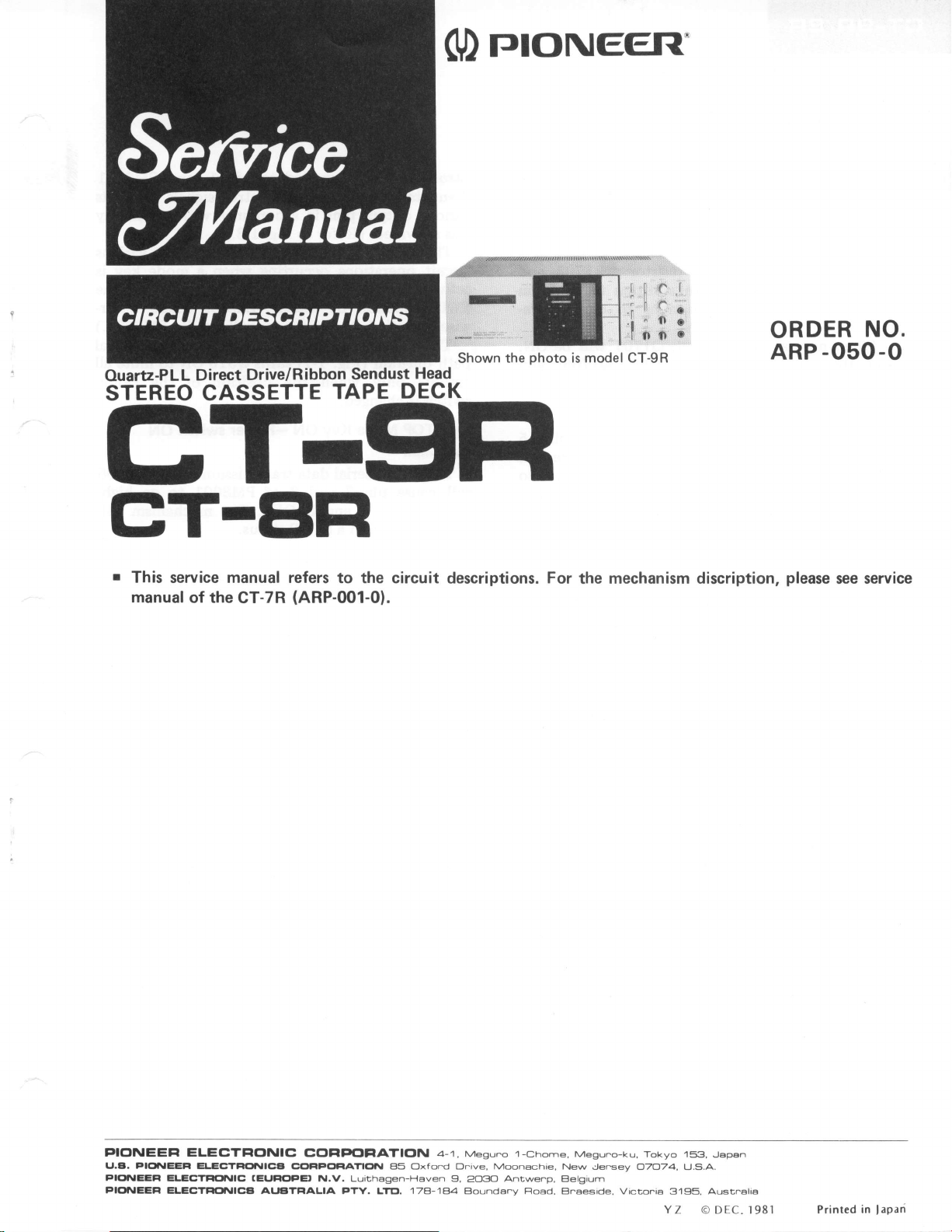
Shown
Ouar?-PLL
Direct
STEREO CASSETTE
Drive/Ribbon
TAPE
Sendust
Head
DECK
eT-tr|trl
lI
GT-8Fl
r
This service manual refers
manual
of the CT-7R
l--rr
(ARP-001-0).
to the circuit
descriptions.
the
photo
is model CT-9R
For
ORDER
ARP
the mechanism discription,
-050
please
see service
NO.
-O
PICINEEFI ELECTFICINIG
U.B. PfCI\fEEFl ELECTFICX\IICB
PICX\IEEFI
PfC fEEFf
ELEC?F|CIN|C aEIJFICIFE
ELECTFICTNICB A|JATF|ALIA
CCIFIPCIFIATICIN 4-1. Mesu.o 1-chome,
CCIFIFCIIIATICIN A5 Oxfond Dnive, Moonechie,
N.V. Luithagen-Haven 9,
PTY.
l.rE,.
178-1A4
Antwenp, Etelgium
2O3O
Eloundeny Fload,
Mesuno-ku, Tokyo 1s3,
New iJensey O7O74, u.S.A.
Bneeside. VictoniE 3195. Aust.alie
YZ
Jepen
ODEC.I98I Printed
in
lapan
Page 2
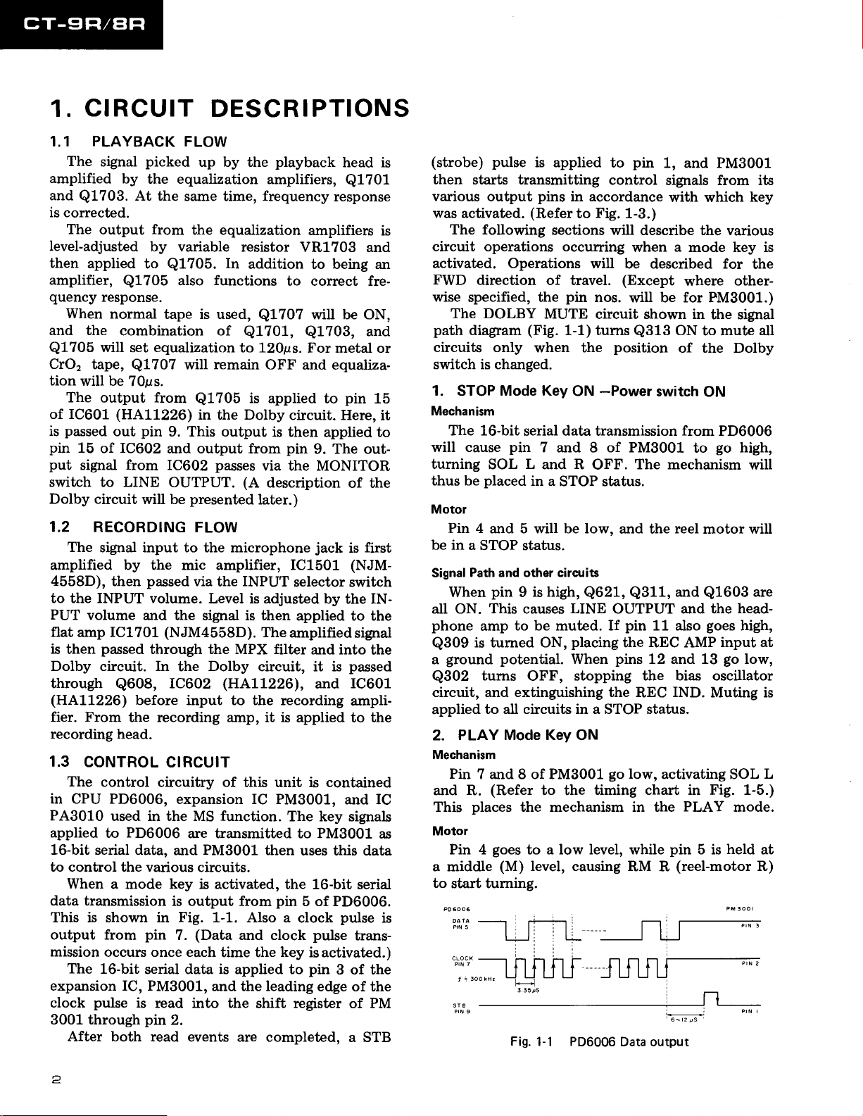
CIRCUIT
1 .
PLAYBACK
1.1
The
signal
amplified
and
Q1703.
is corrected.
The
output
level-adjusted
then
applied
amplifier,
quency
and the
Q1705
CrO2
tion
of IC601 (HA11226)
is
pin
put
switch
Dolby circuit
1.2
amplified by the mic amplifier, IC1501
4558D),
to the INPUT volume.
PUT
flat
is
Dolby circuit. In
through
(HA11226)
fier. From
recording
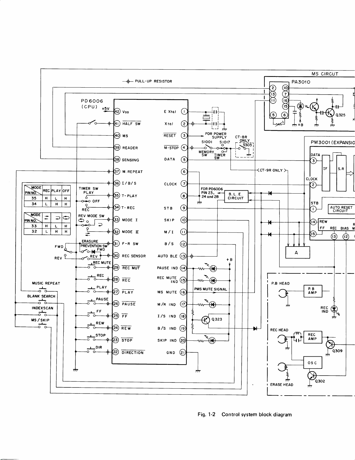
1.3
in CPU PD6006,
PA3010
applied
16-bit serial data,
to control the various
data transmission
This is shown in
output from
mission
expansion IC, PM3001,
clock
3001 through
response.
When
will
tape,
will be
The
output
passed
16 of
signal
to
RECORDING
The
signal input to the microphone
volume
amp IC1701
pa.ssed
then
CONTROL
The
control
When
The
16-bit
pulse
After both read
picked
by the equalization
At the
from
by variable
to
Q1705.
Q1705
normal
combination of
out
IC602
then
Q608,
head.
used in the MS function.
to
a mode key is activated,
occurs once each
tape is used,
equalization
set
Q1707
70ps.
from
pin
9. This output
and output from
from
IC602
LINE
PD6006
OUTPUT.
will be
passed
and the signal is then
(NJM4558D).
through the MPX filter
before input to the recording
the recording amp, it is
CIRCUIT
circuitry
pin
serial data is applied to
is
read into the
pin
DESCRIPTIONS
FLOW
up by the
same time,
the equalization
In
functions
also
remain
will
Q1705
in
the
passes
presented
FLOW
via
the
Level is adjusted
Dolby
the
IC602
expansion IC PM3001,
and
is output from
Fig.
7.
2.
(HA11226),
of
are transmitted to PM3001
PM3001
circuits.
1-1. Also
(Data
time the
and the leading
events are completed,
playback
amplifiers,
frequency
amplifiers
resistor
addition to being an
Q1701, Q1703,
to 120ps.
is applied
Dolby
(A
INPUT
this unit is contained
and clock
shift register of PM
VR1703 and
to correct fre-
Q1707
OFF
via the MONITOR
description
later.)
The
circuit, it is
then
wiU be ON,
For metal or
and equaliza-
to
circuit. Here,
is then
pin
key
applied to
pin
9. The out-
jack
selector switch
by the IN-
applied to the
amplifiedsignal
and into
and
applied to the
The key signals
uses this data
the 16-bit serial
5 of PD6006.
a clock
pulse
isactivated.)
pin
edge of the
head is
Q1701
response
is
and
pin
15
it
of the
first
is
(NJM-
the
passed
IC601
ampli-
and IC
as
pulse
is
trans-
3 of the
a STB
(strobe) pulse
then starts transmitting
various
was activated.
circuit operations occurring
activated. Operations
FWD
wise
path
circuik only
switch is changed.
1. STOP Mode Key
Mechanism
will cause
tuming
thus be
Motor
be in
Signal
all ON. This causes
phone
Q309
a
Q302
circuit, and extinguishing the
applied
2.
Mechanism
and R.
This
Motor
a middle
to start turning.
P06006
output
The following
direction
specified, the
The DOLBY
diagram
The 16-bit
SOL L and R
placed
Pin 4
and 5 will be low.
a STOP
Path and other circuits
When
ground potential.
pin
amp
is tumed ON,
tums
to all circuits in a STOP status.
PLAY Mode Key ON
Pin
7 and 8 of PM3001
(Refer
places
Pin 4
is applied
pins
(Refer
sections
of travel.
pin
MUTE
(Fig.
1-1) tums
when the
serial data transmission from PD6006
pin
7 and 8 of PM3001
in a
STOP status.
status.
is high,
9
to be muted. If
OFF, stopping
to
the
the mechanism in the
goes
to a low level,
(M)
level, causing
3 35)S
Fig. 1-1 PD6006
to
control
in accordance
Fig.
to
will describe the various
will be described for
nos.
circuit shown in
position
-Power
ON
OFF.
and the
Q621, Q311,
LINE
OUTPUT and the
placing
When
pins
go
timing chart in Fig. 1-5.)
Data output
pin
1, and PM3001
signals from its
with which
1-3.)
when a mode key is
(Except
will be for PM3001.)
Q313
The mechanism
pin
the REC AMP
REC
low,
while
RM R
where other-
ON
to mute
of the Dolby
switch
11 also
12 and 13
the bias oscillator
ON
to
reel
motor will
and
Q1603
goes
IND.
activating SOL
PLAY
pin
5 is
(reel-motor
t--"=
key
the signal
go
high,
will
head-
high,
input at
go
low,
Muting is
mode.
held
the
all
are
L
at
R)
Page 3
\ODE
PINNO\
35
34 L H
\{o.
)IN
NO\
33
32 L
rEc
H
H
)LAY
L
D
L H
H
CFF
H
H
H
PD
(
cPu
6006
)
+sv
PULL-UP
HALF
SW
MS
READER
SENSING
M.
REPEAT
I/B/S
T-
PLAY
T-
REC
MODE
I
MODE
tr M/T
RESISTOR
-STOP
M
DATA
STB
SKI
MS
CIRCUT
PA301
0
FOR POWER
SUPPLY
sroot
-{
-€
"tO----O+-O?t
MEMORYO-JIII;
swI|MERli-
sw t'-
P
stotT
-ci-"
B.L.E.
CIRC U IT
CT-8R
--oNLY
qs-orl
i
qr
,-€
_t__t
PM3OOl
I
(EXPANSIO
ArJro
t
crRcu rT
I
REW
FF
REC
RESEI
BIAS M
R
MUSIC
BLANK
SEARCH
.J_
INOEXSCAN
MS
/SKIP
REPEAT
PREVENTION
FWD
REV
-rEEC
REC
-r-
PLAY
4
+PAUSE
. FF
REW
_L
-gSTOP
.J-DIR
MUTE
F-R
SW 8/S
REC
SENSOR
PAUSE
FF
REW
STOP SKIP INO
DIRECTION
AUTO
BLE
PAUSE
IND
REC MUTE
tN0
MS
MUTE
M
IND
/R
T
IND
/S
IND
A/S
G N D
REC
t_
HEAO
ffi
vl
L
HEAD
REc
Fig. 1-2
Control system block
diagram
Page 4
MS
CIRCUT
REEL
MOTOR
CIRCUIT
Path
Signal
When
turn
LINE
pin
constant
PLAY
same
and other circuits
pin 9 goes
OFF, enabling
OUTPUT
goes
16
of the
mode. Pins
state as STOP key
and at
high,
blank
low,
Q621,
sound
the
q324
tums
detector circuit
pin
11,
12
ON.
Q311
to
be output
headphone
ON and
pin
and
and
jack.
enters
13
are in
Q1603
from
When
the time
the
the
PM3OO1
CLOCK
(EXPANSION
AUTO
crRcu rr
CIRCU IT
I
RESET
J lauroRESETl I lsoL.
Gto*'
FF
REC
BIAS MUTE
IC)
r- |
MUTE
I
L
^
il-:l,
{
SIGNAL
CAPSTAN
L
---
MOTOR
REAL TIME
TAPE
RUN
PATH
PA2009
PA201c.
MOTOR
CIRCUIT
NE
,,.o.
|
cr-eR
I
&
MECHANISM
COUNTER
CIRCUTT
HEAD
PHONES
AMP
DOLBY
MUTE
I
oNLY
I
PATH
LI
NE
OUTPUT
HEADPHONES
rI
R
chl
i7
__J
I
3. FF Mode
Key
Mechanism
Pin
SOL L
nism in
goes
7
OFF and
a PAUSE
Motor
goes
Pin
L
in
Signal
Same
4.
REW
4
a
Path
low
STOP
and other
as in
the
Mode Key
Mechanism
Pin
SOL
nism
goes
7
L
OFF and
in a PAUSE
Motor
Pin
RM L
Signal Path
Same
goes
4
ON and
and other
as in
the
5. REC/PLAY
Mechanism
Same
as PLAY
Motor
Same
Signal
When
turned
and
the headphone
muting
signal
and 13
bias
erase head
REC IND
PAUSE
6.
PLAY
as
Path
and
other circuits
pin
9
OFF enabling
is lifted
to be recorded
go
high,
oscillator
and bias
(LED)
Mode
Mechanism
Pin
7
and
8 both
and
placing
OFF
Motor
Same
as
STOP
ON
high
SOL
status.
and
status
circuits
STOP
high
SOL
status.
high
places
circuits
STOP
Mode
Mode
Mode
is low,
from
Q302
and
is
also
Key
the
status.
pin
and
R ON,
pin
5
and causing
status.
ON
pin
and
R ON,
pin 5 goes
and
RM R in
status.
Key
ON
Key
Key
Q621,
output from
jack.
If
the
REC AI\4P allowing
on the tape.
is
turned
applying
to
the recording
illuminated.
(in
ON
go
high,
mechanism
goes
8
low.
placing
goes
high,
RM
goes
8
low.
placing
low.
a
STOp
status.
ON.
ON.
Q311,
and
LINE
pin
11
also
When
ON activating
erase
current
STOP status)
turning
SOL L and
in a
STOp
This
turns
the
mecha-
placing
to turn.
R
This
turns
the
mecha-
This
turns
Q1603
OUTPUT
goes
pins
to the
head.
status.
RM
are
low,
the
12
the
The
R
Page 5
Path
Signal
Same
illuminated
7. PAUSE
and
other circuits
as
STOP
however.)
Mode Key
Mechanism
Pin
SOL L
goes
7
OFF and
high,
nism in a PAUSE
Motor
Same
as
STOP status.
Signal Path
Same
nated
as
STOP
however.)
8. REC/PLAY
Mechanism
7
goes
high,
and
Pin
SOL L OFF
nism in a PAUSE
Motor
Same as
STOP status.
status.
ON
and
SOL
status.
status.
PAUSE
and
SOL
status.
(The
(in
PLAY
pin 8 goes
ON,
placing
R
(PAUSE
Mode Key
8
goes
placing
pin
R ON,
PAUSE
status)
low.
This
the
LED
ON
low.
This turns
the mecha-
LED
turns
mecha-
is illumi-
is
Path
Signal
When
all
ON. This
phone
Q309
ground
a
turns
Pin
pin
amp
is tumed
OFF,
goes
13
and other
to be
potential.
nate.
9. Direction
Mechanism
Pin
goes
27[msec,
goes
STOP to
goes
7
high. This
and
through
REV-STOP.
Motor
Same
as
STOP
Signal Path
Same as
and
STOP
circuits
9 is high,
causes
Q621,
LINE
muted. If
placing
ON,
When
stopping
high,
Key
low for
causes
since
the
causing
(in
ON
a
SOL
SOL R is
a direction
status.
other circuits
status.
Q311
OUTPUT
pin
the
pins
12
bias
the
REC
STOP
275msec
L to turn
OFF,
operation
and
and the head-
11 also
REC
AMP input
goes
oscillator
IND
status)
interval,
ON for
the
mechanism
from
Q1608
goes
high,
low,
QB02
circuit.
to illumi
pin
and
FWD-
are
at
8
only
Pin
No.
FUNCIION
RM.
5
RM.
HEAD SW
7
SOL.
I
SOL.
9
P B. IVUTE n
to
LINE MUTE
II REC
I2
t?
t4
t6 PLAY
PD
t4 PAUSE
MUTE
BIAS
REC
REW
IND
oo6
STO P
'
FWD
IREV
L L
R
L d
R
IND L
IND L,ora,
IND
-
L
-
t
H
L
L
L
H
(
(or'
t
uooE
(OFF)
(oFF)
(oN
(OFF)
(or'
IOFF)
rorr)
(OFF
OFF)
(oN)
(oN)
FWD
HL
LH
)
)
FF
V
FwD I REV
IRE
L n
n
L
HL
L]H
H H
n H
n
L
L
L
H
L
n
REW
FWO REV
L
L
H
L
L
n
L
L
H H
PLAY
L
M
M
L f,
L
L
L
L
H
L
L
L
L
H H
REC,/PLAY
FWO
REV
L IM
ML
L
L r
L
L
L
n
L
L
n
STO P
PAUS€
FWD I REV
L
L
L
n
H
f, H
n
L
L
L
L
L
L
PLAY
FwD I REV
L
L
L
Hlt-
LH
H H
H H
L
L H
L
L
L
L
REC /PLAY
PAUSE
FWO I REV
L
H
HL
L
IH
L
L
L
L
L
L
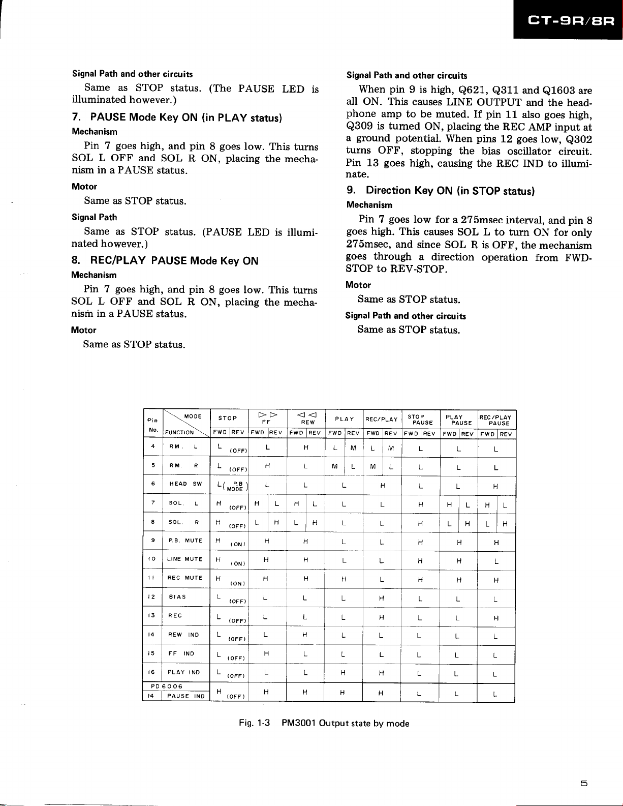
Fig.
1-3
PM3001
Output
state by mode
5
Page 6
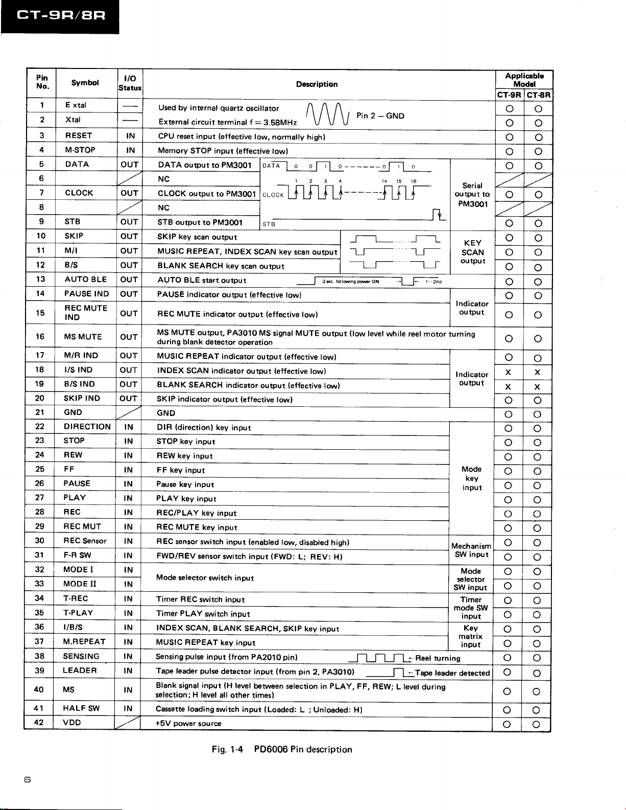
Pin
No.
1
2 Xtal
3
4 M.STOP
5 DATA
6
7
I
I
10
11 M/l
12 B/S
13 AUTO
14
15
16 MS MUTE
17 M/R IND
18 r/s
19 B/S IND
20 SKIP IND
21 GND
Symbol
E
xtal
RESET
CLOCK
STB
SKIP
BLE
PAUSE
REC
MUTE
IND
rND
OUT
OUT
OUT
OUT
OUT MUSIC
OUT BLANK
OUT AUTO
IND
OUT
OUT REC
OUT
OUT MUSIC
OUT
OUT BLANK
OUT
22 DIRECTION
23
STOP
24 REW
FF
25
PAUSE
26
PLAY
27
REC
2A
29 REC
30
31 F-R
32 MODE
33 MODE
MUT
REC
Sensor IN REC
SW
I
II
34 T.REC
35 T.PLAY
36
r/B/s
37 M.REPEAT
38 SENSING IN
LEADEF
39
40
MS
HALF
41
42
SW IN
VDD
vo
Used by internal
External
IN
IN Memory
IN
IN
IN REW
IN
IN
IN
IN
IN REC MUTE
IN FWD/REV
IN
IN
IN
IN
IN
IN
IN Tape
IN
CPU reset
DATA output
NC
CLOCK output
NC
STB output
SKIP key
PAUSE
Ms
during
INDEX
SKIP indicator
GND
DIR
STOP key
FF key
Pause
PLAY
REC/PLAY
Mode
Timer REC
Timer
INDEX
MUSIC REPEAT
Sensing
Blank
selection; H level
Cassette loading
+5V
circuit
input
STOP input
scan output
REPEAT,
SEARCH key
BLE
indicator
MUTE
MUTE output, PA301o
blank
REPEAT
SCAN
SEARCH
(directionl
input
key input
input
key
input
key
sensor
selector
PLAY
SCAN,
pulse
leader
signal input
power
Description
quartz
oscillator
terminal f
(effective
PM3001
to
to
PM30O1
to
start
output
output
indicator
detector
indicator
indicator
output
key
input
key
input
key
input
switch input
sensor
switch
switch input
switch input Timer
switch input
BLANK
key
input
pulse
detector
(H
all other timesl
switch
source
:
3.58MHz
low,
normatly high)
(effective
tow)
orrr
--t
SCAN key
scan
output
(effective
output
MS
operation
output
output
(effective
(enabled
input
SEARCH,
inpur
PA2010
input
level
between
input
.'^^ulilAlAlA
STB
(effective
signal
(effective
low)
(FWD:
(from
(Loaded:
PM3001
INDEX
indicator.output
input
(from
l1___1J-
1234
T-'l r-t rr I
UUU
scan output
[
low)
low)
MUTE
(effective
lowl
(effective
tow,
disabled
L;
REV: H)
key
SKIP
pin)
pin
2,
selection in
L ; Unloaded:
rl_
ffi;;,pffi----
output
lowl
lowl
input
PA3010)
Pin
2 - GND
g
- -
- - --_Sf;Lr_
J--L
-L-
---1__J-- --t_r
(low
level
high)
J-l_l-Ll-L
PLAY,
FF,
REW;
H)
while
n
L level
r[_
_J__-L
-Lr
l=]-fr"
reel motor
Reelturnins
*Tape
leader
during
Serial
output
PM3001
KEY
SCAN
output
I ndicator
output
turning
Indicator
output
Mode
key
input
Mechanism
input
SW
Mode
selector
input
SW
mode
input
Key
matrix
input
detected
SW
to
Applicable
Model
CT-gR
o
o
o
o
X
X X
o
\J
o
o o
o
o
CT€R
o
o
o
o
o
o
X
o
o
o
o
o
o
o
o
o
Fig.
1-4
PD6006
Pin
description
Page 7
Timing
PIN
NO.
,,N
chart
1
FWD
POWER
STOP
ON
Its
STOP REW
STOP
P
LAY
STO P
PLAY
PAUSE
/
STOP
4 RM
R tvl
6
HEAD
7
SOL, L
I )vL. x
I
Zu
gF
*s
g6
9 P
lo
tl
PAUSE
DIR
STOP
B MUTE
LINE MUTE
REC MUTE
R
SW
Tr
L
=
H
H
STOP
H
H
H
Tt
tl
-.,r
l*
PAUSE
,
I
L
L
L
L
L
L
f
Tl
i*M
t2
1F-
*l
PLAY
l*
f2
'l-1
TI
Tr
T2
T6
'Ati
Tll
tl I
t,t I
'lll
-
f
-l
-
_l_
t2
t3
BIAS
REC
SW
L
L
ft:425mS
T2:275mS T!:275mS
Fig.
T4:225mS
T5:tASmS
T6:42SmS T7:42SmS
1-5 Timing chart of PM3001,
Ts:325mS
Te:ZgmS Tto:l25mS
1
7
Page 8

Timing chart 2
-NooE
PIN
NO.
FUNCTIOiI \-
4
RM
L
FWD
STO
L
P REC
/ PLA Y
STOP
PLAY
PAUSE
/
REC/PAUSE REC /PLAY
PLA Y RECl PLA Y ?EC /PAUSE
STO P
f,
RM.
R
HEAO
SW
7
SOL.
L
R
SOL. R
=
z;
g<
$o
=
9
to LINE MUTE
tl
t2
PLAY
PAUSE
DIR
STOP
PB. MUTE
REC MUTE
AS
BI
L
L
H-
n
STOP
H
H
H
L
Jz-
r9
M
t*
Tg-
r
r
PLAY
t,
+
I
k-!
l*
rl
--l_
-t_
,
t
,
PAU
T9
SE
Tr
I
L
T2
M
fe
|*
a
I
I
I
.l*---
I
I
-l
t:
Tz
It'"
T
Tsr
r8-
f
to-
it
il
t-
Te
-{
I
Tl
t
REC SW
T9
t9 T9
Fig.
T9
Timing chart of
1-6
PM3001,
T9+
2
,9
a
Page 9

Timing
PIN
chart
---_\MO0E
NO
FUNCTION
4
RM.
5 RM. R
A
HEAD SW
3
\:
L
FWD
STOP tt
L
LT
n
lH
t
rs-
H
REW
H
tM
T5
FF PLAY
lr
lt Fr.
ili
Tt .
M
REW
t
REW
FF
REC
/ PLAY REW
Tl
lr-
r-r
FTz
irl
llTg-
r
Fl
I
7
E
a
2P
ii
H;
9 P
to
tl
t2
t?
SOL.
L
SOL. R
PLAY
DIR
STOP
B. MUTE
LINE MUTE
REC
MUTE
BIAS
REC
SW
H
Tl
Tr
ih
H
I
PAUSE
I
STOP
n
F
H -l
L
L
Fig.
1-7 Timing
Tr
ll
tl
PLAY
il
',
ll
if
I
I
"l
h_
."*i
L
chart
of
I
I
\L
pM3001,
Ts
f3
l-
r9 Te
3
I
I
I
-
+r
it,
I
"t
t6:
I
t
Ll
t
Page 10

Timing
PIN
NO.
FUNCTION\
RM
chart 4
L
FWD
STOP
L
REV
STOP
FWD
STOP
FWD
PT^Y
PAUSE
REV
PLAY
/
/
PAUSE
FWD
PLAY
PAUSE
FWO
/
REV
FF
FWD
FF
tt
t2
F
=
I
z
U
=
to
d
5
7
RM
HEAD
SOL
SOL R
F- PLAY
F. DIR
STOP
R-
OIR
-PAUSE_
R
R.PLAY
P.B
MUTE
LINE
MUTE
REC
MUTE
BI AS
R
SW
L
-
_
L
L
H T2'
n
tl
ii
iil
it
ii
'rdr
I
I
2
Tg
f
T2=
T3-
tu
T
U
I
I
I
I
-t
'r?
.1
I
I
I
{rr
o',,i-j
il-
-l
REC
SW
DIR:0IRECTION
L
r%;l
l'wo*--l
PLAY
I
Fig.
1-9 Direction
Tt:425mS
I
operation
Ta:275mS
T.:275mS
Fig.
F**-l
t"%*--f
(in
STOP status)
T4:ZZ5mS
1-8
Timing
T5:tASmS
chart
of
Fis.
T6j42SmS
PM3001,4
1-10
Direction
status)
T7:425mS
operation
Ts;325mS
(in
PAUSE,
Ts:Z5mS
FF
Tro:t25mS
and REW
10
Page 11

Timing
chart
5
PIN
NO.
FUt'tCTtOt't-
RM
f,
RM
HEAD
7
SOL.
I SOL.
U
F
s
2
z
=
lo
LINE
tl REC
L
SW
L
R
F-PLAY
F.PAUSEF.DIR
R-
DIR
R.PAUSE-
-PLAY
R
B, MUTE
IVUTE
MUTE
-
-
-
_
FWD
REW
L
L
H Tz-
L
n
n
d
REV
t!
L
REW
iir
'{li
FWD
REW
u]
i
i;
"il
FWD
PLA Y
T2
Tr
REV
i-l
iii
rr\
rrl
a
PLA Y
t
I
I
l1
T2
i
l_
l-Tz
Tl
L
FWD
il;i-
',
ilT
a
lf
P
LAY
ii
Fig.
t3
1-12
BIAS
REC
L
SW
DIR : DIRECTION
Direction
operation
Fig.
1-11
(in
PLAY
Timing chart
status)
PM3001,
of
5
FWD-REV
-FWD
REV
+
--*
Page 12

1.4 TAPE
The
the
auto-reverse
transition
portion
to reverse
in a
STOP
fast-forward
LEADER DETECTOR
tape leader
from
of
the tape.
the direction
status
(FF)
The detector
infrared
LED
phototransistor.
ing
a difference
the coated
by the
portion
transparent
The output
to light
shown
transistor.
received
the input
the charge
held
output from
pil$es
picked
creases
high,
terminal
then
connected
input level
When
the
snaps from
taken
CPU PD
the various
nical
by the
in Fig.
During
by the
level
presenting
low,
terminals
into
up
the
input to
consequently
of the comparator.
goes
high.
the level
+
terminal,
from
functions
and voltage
of comparator.
pin
the light
by the
to
to the
high
pin
6006
mechanisms
stop.
LED
JN---:;:\
Fig.
1-13
detection
mode
the
to detect
coated
It then
portion
directs
oftravel,
when this
or
rewind
uses
an
event
(REW)
optical
whose emission
The
circuit is
in the
amount
of tape,
and the
leader.
pin
from
LED,
1-13
16 of PA3010
passes
and
picked
to be
tape travel,
phototransistor
pin
at
7 is held
pin
at
a low logic
But
2.
as the
path,
phototransistor
pin
7.
This causes
applying
pin 3 goes
As
pin
4
starts
-
terminal
of the
the
output from
to low,
2 appears
uses this
-
terminal
as
output
a high
charging,
and
performing
of
auto-reverse
REFERENCE
_
-l
Tape
t
TAPE
Eb
.5
enase nero
1-6jJl
n lwrrH
PIIOTOTRANSISTOR
leader
detector
CIRCUIT
circuit
functions
point
the
to
the leader
the mechanism
places
or
the
occurs from
mode.
system based
picked
is
activated
of light
up
by detect-
passed
amount
is converted
through
up by the
the
is
low.
3 and 4
input
This
amount
quite
results
the
photo-
of light
small,
This
to
also be
to the + and
in a low
transparent
the
amount
of light
suddenly
pin
3
to
input
to the
Output from
high,
the capacitor
raising
of the comparator.
reaches
that
the comparator
the output
shown
in Fig.
pulse
to control
the
mecha-
and automatic
PIN
wrNDow
section
in
of
unit
the
on
an
by
by
passed
path
so
causes
leader
in-
snap
+
pin
2
the
of
pulse
1-1b.
PA3010
.
a
PIN
NO
t6
4
_--_!'
END
1.5
Since
tape leader
status
or
reaching
activated,
not operate.
the
cassette
difference
between
the
tape,
before
circuit
the
is
When
pulse
is transmitted
(used
to control
PD6006. (This pulse
and
shaped
When
high
this
(H)
PD6006
tape
and
PHOTOTRANSISTOR
Fig. 1-14 Tape leader
.or
1r1-L-=----
l-t
COATEO TAPE
Fig.
1- 1
5 Tape leader detector
SENSOR
CT-9R
detector
go
through
point
the
so normally
However,
tape,
in the
the coated
or in
tape leader
then
activated.
the
reel
into
pulse
level
for
interprets
thus
switches
CIRCUIT
and
CT-8R
circuit,
a direction
where
the
where
or where
infrared
portion
case
the reel
is detected,
motor
from
the reel
is taken
a squaxe
is
maintained
period
a
that to
to the
t,l-e end
end
there
starts
pin
exceeding
detector circuit
o B
r_
LEANR TAPE
waves
are equipped
go
they
into
operation
sensor
sensor
there
is no
is an
circuit
insufficient
transmission
and leader
motor
stops rotating
the end
tuming,
13
of IC
motor)
from
wave
at
to
the Hall
by PA2010.)
either
a low
three
mean
next
the end
mode
with
a STOP
before
cirucit
leader
factor
portion
sensor
a sensing
PA2010
pin
88
element
(L)
seconds,
of
of
opera-
a
is
will
on
of
of
or
the
tion.
l4
Page 13

If
?
(FF),
is
it
reverse
If
the mechanism is in the
rewind
mode.
presently
(REW),
or
the next mode entered is STOP.
in the PLAY mode and the
fast-forward
record-playback
(REC/PLAY)
mode switch is selected, it also enters the STOP
mode. But if
a direction
are selected, if first
?
Q
,
operation, then into
goes
a PLAY
through
status.
Consequently,
pin
13 is at
high
output.
when an
a low level,
output
This
function operations
BLANK SEARCH,
PMS MUTE""'
L
MUSIC REPEAT).
(PIN
(8LANK
II)
input signal
and no signal
is
produces
is used by each
(MS/SKIP, INDEX
OPERATION )PMS
SEARCH
MUTE
present,
of the
SCAN,
',,'H
(
PIN
I I )
a
RIGHT
REEL
MOTOR
HALL
ELE MENT
1.6 BLANK
When
reel
goes
the
motor starts tuming,
to a low level. When
of the blank detector
lifting MS
PA20to
Fig.
1-16 End
DETECTOR
function key is
IC
(Music
Search) muting and commenc-
ing MS operations.
As
fied,
mined by the
parator
MUTE is lifted, the signal is first ampli-
MS
then applied to
pin
comparator
output at
point
Fig. 1-18.
This output is used
to tum Tr1
turn allows capacitor C
dump its charge through
Tr1.
a low level.
When there is no input signal
OFF, capacitor C
mately
pin
7Omsec
13.
starts recharging, and approxi-
later, a high level is output from
_|LJ-L
P06006
diagram
sensor
IC PA3O1O
placed
pin
pin
16
(PA3010)
and its level is deter-
9,
in the next
is
A
as shown
connected
Thus,
present,
OPERATION
ON, and the
16 of PD6006
goes
low,
goes
also
stage. Com-
ON, and
pin
to
pin
13
Tr1 turns
pin
low,
in the
this in
!2
goes
11
to
to
9
,,1,l,..1.,,'..,,. .[h/1.,,.
ll
W mlffi ilW
lwwmm mffiilffi
5V
70ms+
-Fr
2
4vf\'
2.5V
3
I
FUNCTION KEY OPERATION
1.7
The various functions
BLANK SEARCH, MUSIC REPEAT)
placing
by
The timing chart for the
10, 11, and 12 of CPU
1-19. As a
tion, a
pulse
the CPU.
pulse
the
mode accordingly.
t1 t
t-t
Fig.
Blank detector
1-18
(MS/SKIP,
the respective key to the ON
pulses
PD6006 are shown
function key is
placed
train is input to either
The
train, and starts
then determines the timing
CPU
operation of the
_J-----r_
-1_I-
-l
r
!e-l
i-
-LJ-
waves
INDEX
output
in the ON
pin
c+
ll,, r,,1. .
--1'
prllrl'n
L
SCAN,
are activated
position.
pins
from
in Fig.
posi-
or 37 of
36
selected
_J---L
-1J-
--l
f
-Lr
of
Fig. 1-17 Blank detector
circuit
Fis.
1-19
MS/SKIP Operation
1.
When
(
>>
a
music
drops
pulse
sets
the MS/SKIP
key is activated,
)
selection
high to low. The
from
effecting
the
the REWIND
is located,
level drop at the
mode
back to the beginning
the PLAY mode.
A=57!S A=AOIS. Cr27oS
Function key diagram
placed
Key
and
is
when
pin
ON,
beginning
the
of
13
trailing edge
PD6006
rewinds the tape
and
of
the selection,
FF
the
of
PA3010
the
of
pin
and enters
Page 14

At the end
section
of the
output from
level
continuously
then
selects
until
the beginning
the
level
at
back
out to
enters
2.
operating
mode
The
to locate
into
starts
the PLAY
INDEX
When
is entered;
unit
the PLAY
and
INDEX
in
then
the beginning
continues
of PA3010
of
the selection, if
tape
pin
13 from
high
the
FF mode,
pin
13 low. It
the beginning
mode.
REW
Fig.
1-20 MS/SKIP
SCAN
Operation
SCAN
the
FWD
if in
REV,
cycles
mode.
for
is held
low.
(functioning
low to high) holds
for over
8 seconds,
continuing
of the
next
then
of the
operation
is activated,
direction,
(
REW
through
of
a
search
a selection,
Playback
the
7
seconds
the unrecorded
to change
PD6006
in that
selection
rewinds
selection,
if
the
<<
mode
drops
(
<<
the
unit
(
FF
>>
is entered.
)
and
operation
goes
then
of
the selection
pin
that
the
the
18
D
I
R
E
c
T
I
N
After
retums
through
tions on
If the
FF, or
)
entered,
search
switch
When
(FF
SCAN is
this 7
to the FF
seconds
or
another search operation
tape
the
are thus indexed.
tape should end
REV
REW,
either the
or a direction
to continue,
depending on
setting.
KEY
in INDEX
in
REV
operated
SCAN operation,
direction)
in
REW mode
has
elapsed, it
REW
mode
while the unit
STOP
status would be
operation
the reverse mode
placed
is
as
once again
and cycles
until all
in FWD
is
would
REW
ON,INDEX
shown
selec-
allow
KEy
in Fig.
r-2t.
3.
BLANK
When
if
the unit
search
ing
in
REV, it
When
13
of PA3010)
the
tape end
is
)
tion of
position
the
snapped
From
mode
the
high
until
blank
level
status, completing
As
shown
recorded
REW
mode
seconds
When
the
leader
mode
and
SEARCH
the BLANK
is
operating
is
started in
is
input
to
sensor is
travel
is reversed,
where
from high
position,
this
point
a
detector
for
4
in Fig.
tape,
the
after
in FF
mode-
detecting
tape
goes
then
Operation
SEARCH
in
the FF
started in
the blank
is held
high for
detected,
input
low.
to
the unit
is
reached
is maintained
seconds.
the
operation.
L-22
tape
retums
the search
the
tape end,
portion
into
the FWD
(
>> ) mode;
the
detector
and the
to the
It then
(3),
had
for
a
STOP.
key
placed
is
direction,
if
operat-
(
REW
8 seconds,
the
(output
present
<< ) mode.
by
or when
tape returns
blank
reenters
detector
the PLAY
where the input
at
a continuously
goes
into
a STOp
in
case
of
the un-
to
0.8
i.- e
the tape
been
the
seconds
sec
done for
tape
-l
end in
travels
in FF
ON,
the
pin
direc-
to
at
8
Fig.1-21
INDEX
SCAN
REW KEY ON
operation
l
LEADEFi
Fig.
i I D.
r8
1-22
BLANK
sec
PLAY
=
SEARCH
operation
IAPE
ENO
Page 15

4.
MUSIC
REPEAT Operation
When the MUSIC
while the unit
present
the
recorded
then
Iow
tape selections) continues to completion,
the output from
to high.
held high f.ot
beginning of that
This
operation may be repeated
is
music selection
After the
2.5 seconds, the unit returns
selection and
selection for up to
REPEAT is
The
end
sensor
STOP
is
cleared and a STOP status
status will
activated.
in the
(or
13 of
key is
PLAY
the next if un-
PA3010
pin
REPEAT
presently
pin
output of
repeats
for
8 times, after which
also be entered in case the
placed
ON
status,
goes
from
13 has been
to the
playback.
the same
MUSIC
entered.
out
put
t
......*
Input
Fig.
1-23
DOLBY
1.8
The CT-9R
C Dolby
type
type C
The
reduced
be
7l<Ilz.
for the
as
difference
cessor
by up to
The basic operating
type
lying in the
stages
stage connected
B Dolby
tapes to
NR
be
and decoding operations
and L-26
L-25
input/output
Fig.
in
The
1-24.
REC
skewing circuit
resonator with an
prevent
level
processor
low to mid-range decoding
leakage) due to high
The
REC
stage
rnto 2 signals, the main
MUSIC REPEAT operation
PROCESSOR
NR
CT-8R
and
processors.
NR
Dolby
both
NR system
20dB
principles
B Dolby
NR system,
use
(a
high
level stage
in series).
processor
played.
enables
also
Block diagxams
are outlined
respectively.
frequency response curves are
passed
srgnal
is
(see
Fig. 1-25) which is an
for
2OWlz, and designed
at
level
signal is then
(high
level stage)
signal being
to adder A, while the main
(side
SCF-1
chain
shoot suppressor C
A where the main and sub
filter),
before
signals are
feature
frequencies
at
type B and
enables noise
above
the same
are
to
the major
to a
encoded
B
encoding
Ftgs.
in
prolevel
type
of two
and
Switching
Wpe
corresponding
The
separate
a low
for
shown
through a
spectral
LC
to
error
(high
signals.
it is
passed
is
B and
the lst
divided
directly
via
over-
applied to
where
passed
signal
arnplifier
being applied to adder
recombined.
Fig.
In addition, the amplifier B output is applied
rectifier E
fier
D, the rectified output being applied to
(voltage
variable
response is
(non-linear
control resistor) of
high-pass filter
varied according to
The VCR value
ditions, and the
determined
by
output will thus
signal level
range will
be
InpuVOutputcharacteristic
1-24
integrating type)
SCF-1.
This
where the
the VCR
is increased
SCF-1
CURI. The
be
(around
under
tumover
level
10dB
higher than the
1.5kHz), and the
low
frequency is
of the adder A
contracted. The VCR value
to
via ampli
VCR-1
is
SCF
frequency
value.
level con-
main
dynamic
will drop
when the VCR control voltage exceeds the
threshold value, and the SCF-1 turnover
frequency
will be increased by C2lC!lR2lVCR-1, thereby
attenuating
low to
mid-range
signal. And since the sub to main signal
lower
degree
higher input signal
at
dynamic range
of
The adder A output
processor
whose dynamic
compressor stage
compress the
stage,
the
VCR-2 control
ing level of the 1st
processor
circuit R.
the same
(low
stage
level stage)
range
is
added.
was
dynamic range
threshold level of the 2nd
voltage is set
processor
stage also
purlpose
The
includes an anti-saturation
of this circuit
improvements
signals in the sub-
ratio
frequencies,
conhaction
is
applied
is smaller.
to the 2nd
the
where the signal
compressed in the
lst
In order to further
in
this
2nd
processor
processor
below the corespond-
stage.
The 2nd
is to effect
as the spectral skewing
circuit.
During
circuitry
1st and
Since
inverter
loop is
playback
is used as
processor
2nd
the circuit
(sub-signal
formed with the sub-signal
(se
Fig. t-26), the
in recording mode,
in
stages
starts
from the output of the
output), a
the
negative
being
same basic
but with the
reverse order.
feedback
subtracted
a
is
15
Page 16

from
the main
path
signal
recording
characteristics
signal in
operation
adder
is exactly the
mode, the decoding
complement
more, the anti-saturation P
characteristics during
decoding
A'. And
since the
same as during
and
each
other. Further-
and
spectral de-skewing
are the exact
sub-
encoding
opposite of
during
encoding.
the conesponding characteristics
Consequently, a flat
response is maintained at all
of the
encoding
and decoding
completed.
levels
opperations
frequency
after all
phases
are
REC IN
P.B.
IN
processor
lst
I
i
scF-
procesor
2nd
A'
Adder
Overshoot
i- tl
D'
Amp.
(high
levet
stagol
Inverter
Adder A
|
Amp. B
Inverter
r\ : I l-l
Overchoot
suppressor
C
g):.,!-
FiS.
t-ZS
(low
lnverter
C'
Amp.
-l[}r*
Rectifier E'l
Block diagram for
lanel
stagel lst
Antisaturation
scF-2
B'
t+
+
P
2nd
| |
ii
rl
ll
tl
tl
gl
rl
tl
tl
ii
tl
ll
tl
tl
rl
encoding
processor
I
I
I
I
I
I
I
I
I
I
Overshoot
I
I
suppressor
I
I
I
I
I
J
I
I
I
I
I
;"".iri"reE
processor
salgelenR
saruralton
R4
(low
Ft
c6
,thln
iJn""tirier
operation
(high
Adder A
C
Amp.
||
level
Adder
Amp.
B'
lovel
stagel
I
-l*L
stagel
A'
Overshoot
suppressor
L=
E,
Amp. D,
scF- |
REC
OUT
Spectral
de-skewing
PB.
OUT
16
Fig.
1-26 Block diagram
for
decoding operation
Page 17

1.9
AUTO BLE
Auto BLE
recording
level and equalization
CIRCUIT
provides
the
recording characteristics
type formulations.
When
the AUTO key is
mitted from
initiating
mechanism
recording level.
Bias is
mined
to
and
The
set by detecting the
by subjecting the
record/playback
selecting which of
resistance
This adjustment
four
times. Then after
Operation is
PD4010
operation and coarse-adjust
It
then shifts to bias adjustment.
at 16 step levels
the 16 bias strengths is best.
of the bias circuit is
cycle may
function
of
setting
bias,
to obtain the ideal
exhibited
pressed,
by the
fully
a signal is
various
automatic.
trans-
to control IC PD6006
ideal current, detertone
lkHz
oscillator
intensity
of
signal
set accordingly.
repeated
be
equalization has
up to
been set,
in
the
tape is rewound
complete
20
seconds.
In
AUTO BLE
The
adjustment
case one of the adjustments is
to make, it is automatically
is
tape
then rewound and
to
process
set.
The detection
adjustment consists
method used for each value
passing
of
signal through the Lch
and
comparing
analog voltage
passed
through
obtained from
them
the
(with
D/A
are contained in PM9001.
the
starting
requires from
position.
10 to
impossible
The
for
disabled.
standard
the
values
are
record/playbaek
and Rch rectifier circuits
comparators) with
a CPU digital
converter. These
an
sgnal
circuits
SIGNAL PATH
}IEAD
PM900
MECHANISM PATH
LI NE
OUTPUT
C LEAR
I
CONTROL PATH
n.
osc
Fig.'l-27
B.L.E. circuit block diagram
17
Page 18

The
REAL
CT-9R
1.10
the rotational
pulse
signal
and
real
time
Tape
Counter
o
Tape
counter
oN.
1.
When
ON
the
during
cunent
2.
charge
Q1206
C1218.
collector
3. This
low
(PD6008).
pin
and
4.
This
output
inverting
5.
setting
Thus,
the
the
the
time
TIME
uses
speed
PD6008
to
counter.
Function
set to
power
pass
to
being
is
at a low
signal
Pin
19 is
amplifier
display
tape
power
COUNTER
a HaIl
of
the reel
"0000" at
switch
the
100ms
through
ON
also
level.
is
applied
13
thru
low.
passed
is
to
counter
is
applied
element
sensor
carrier,
for
use
by
the tape
the time
is turned
interval
+B,
R1214,
qL2O7
turns
pin
to
18
of IC904
to LED
of
ICg0b (Mb4b1?p),
"0000,'.
restarts
to
the unit.
from
to
detect
and
inputs
counter
power
is
ON,
e1206
required
R121b
ON,
and its
B of IC904
are high,
1101
via
.,0000"
a
turned
is
for
and
the
at
o
Tape counter
1. As
shown in Fig.
ted
by the Hall element
the right
17 of lC2O2
increment/decrement
reel carrier is
(PA2010)
13.
2. This output
is
(PD6008).
3. At the same
element
6 of IC903
pin
7.
4.
This
output
5.
Signal input
data
to be transmitted
(active
pins
by
display
time, the voltage
(H251
: HA)
(NJM2903)
is applied
pins
to
high),
and digital
26 thru 29.
of the tape
6. When the tape is
tion, the
with
pulse
each tum
shown in
of the reel,
to increase.
7. When
tion,
with each tum
the tape is
pulse
the
shown in Fig.
of the reel,
to decrease.
"nnnn"
L-29, the Hallvoltage
(H252:
applied
and is
applied to
HB)
pins
to
output from
pin
32 of. IC904
generated
is applied
to
and is output from
pin
to
and
30
by
data to be
This changes
30
32 cause segment
pins
13 thru
transmitted
the numerical
counter.
traveling in
Fig.
the
1-29
FWD
causing the
traveling in the
REV
1-29
causing the
genera-
built
into
16 and
by Hall
pins
5 and
of
IC904.
direc-
is applied
counter
direc-
is applied
counter
pin
1g
IC9o4
PrN
30 rNPUl|
rcao4
',1u,i3.,
f--'l fi --.1
J
Fig.
1-28 Tape counter
'no
16r)-l
l\<tYl
L_t
LJ L
Ll l_J
COUNTER
INCREMENT
function
too
coLUMN
(
UNITS
)
to2
coLuMN
(
HUNORES
)
ro!
coLUMlt
(
4-
PULL-UP
rHousaNDS
R€SISTOR
)
"ula=-ol
lC904
PIN
30
JI-I]JA
IN PUT
IC904
PIN
L
32
INPUT
Fig.
1-29 Tape counter
increment/decrement "nnnn"
ROTOR
MAGNET AND
HALL
ELEMENT
RELATIONSH
IP
HR
7C202
13
PIN
OUTPUT
ffi
m
18
Page 19

a
Counter reset
1. When
placed
a
pin
2. Thus,
counter
"0000".
IC904
the counter
Real
the counter
pin
ON,
low level,
and
19low.
when 51101
unconditionally resets the counter to
However,
continues, and when
will
Time Counter Function
reset
41 of IC904
pins
13 thru 18
is
held
real time operations by
once
again
When the Counter/Mode
placed
tape counter or real time
ON, the counter can be
Placing
1.
(PD6008)
51102 ON causes
to drop low.
counter operation.
2. This causes a high output from
illuminating the
Q921
ON,
indicator.
If
3.
the tape is traveling, voltage
right
reel carrier Hall element
input to
and output is
4.
At the same time,
element
applied to
from
5. The outputs noted
pins
to
they are
amount of tape
output
6. During the few
cessing is
no data
output from
and low, switching
the dot
pins
5
and 6 of IC903
from
voltage
generated
the
and 3 of IC903, with output
pin
(HA
pins
1.
obtained
:
H253) of
2
in 3 and 4 above
and
30
from
31 of IC904
processed
time
pins
13 thru 19,
to obtain data on
remaining.
second interval
taking
present
place
in step 5 above,
in IC904, and this causes
pin
2O to vacillate between high
ON and
Q921
indicator to blink. This reports initial
data acquisition.
7. During the time
numerical display will show
the
data,
switching to an accurate
calculation result a
8. As the
processed
dot indicator is blinking,
the
few
seconds
data is stored in IC904,
20 will be locked high and
keeping the dot indicator
ON
reports the
This
real
ing
time.
9. Remaining
during
tape
10. The unit
PLAY
second
mode
units
1l.If during tape
fact
that the counter
tape time is continually
travel to update
indicated by the counter during
is seconds.In the FAST mode,
shown.
are
travel, the
mode is entered. the counter
switch
(S1101)
(PD6008)
go
high, with
down,
S1101
indicate
switch
switched
pin
the tape
is released,
real time.
(S1102)
to eigher
40 of IC904
pin
20
LED1101 dot
generated
(HA:
H251)
(NJM2903),
pin
7.
by the Hall
left reel
carrier is
are applied
(PD6008)
This data is
and 26 thru 29.
that
data
OFF causing
preliminary
display of the
later.
Q921
will
illuminated.
is indicatprocessed
the counter.
STOP
or
will hold the
drops to
to turn
by the
where
the
pro-
there
the
pin
remain
the
10
PAUSE
is
is
is
point
value at the
l-2. When the
tape reaches the
the counter, the
for
approximately 30
slight
differences
the tape may continue
o
allow
CAPACITY switch
TAPE
TAPE
The
for
various tape
CAPACITY
the tape time remaining
ON and OFF
and
39
o
Tape travel direction indicator
produces
of IC904
Fig.
1-30
LED indicators are
can determine whether
FWD or
1. During
direction.
REV
the FWD mode of travel, the
signal waveforms
is
(PD6008)
are as shown in Fig.
2. These signals cycle through
of entry.
"00.00"
"00.00"
in
display will be
seconds
length
tape
to account
traveling).
switch
lengths to
(S1018)
processed
be
display. Switching S1018
the logic
(PD6008)
levels at
shown in
Tape capacity switch
provided
the
from
so that the operator
tape is traveling in the
pins
9 thru L2 otIC9O4
1-33.
Q914
point
(even
is used to
Fig.
thru
held
for
though
for
pins
1-30.
output
Q916,
on
38
turning them ON and OFF, thereby illuminating D1
of
tion
During the
3.
signal waveforms
IC904
4. These signals cycle through
turning them
ing D4 thru DG
of
tape travel.
5.
blinking rate
The
by
the mode the mechanism
information
D3
thru
to indicate
tape travel.
mode of travel, the output
REV
(PD6008)
are as shown in
ON and OFF, thereby
indicate
to
of D1 thru D6
is received through
from
the forward direc-
pins
9
thru
Fig.
Q914
thru
illuminat-
reverse direction
the
is determined
is in,
pins
and this
thru
33
of
L2
1-34.
Q916,
37
of IC904.
19
Page 20

REV
PLAY
REW
PAUSE
Fig.
1-31 Tape travel
direction
indicator
FwD rNDrcaroR
+
TNoTCATOR
REV
€
MECHANISM
o
3
r
G
a
Memory
MODE
P
STO
REW
PLAY
FEL
PLAY
PAUSE
PAUSE
REC
PAU
SE
STO P
REW H
PLAY
PLAY
PAUSE
PA
USE H H H
Fig.
1-32
stop
When the MEMORY
ON, the tape
in
reaches
the
fast
"0000"
may
mode, automatically stopping
on the tape counter.
33
L
L H
L H H H
L
L
L
L
H
H H H
n
be
PD6OOB PIN
INPUT PIN
34 35
H H
L H H SEE FlG.
H
L
L H H
H
L H
H H H
H H H
n L H H
H H
H H
L
PD6008
input/output
switch
(51001)
moved ahead or backed
AIso, when the counter indicates real
tape can be moved in
equivalent
to
"0000",
fast
the
mode to the
where it is automatically
stopped.
1. When the tape is
level output is
(PD6008)
produced
when
in the
fast
travel
from
the tape counter reaches
"0000".
2.
This output
(S1017),
where it is
3. The low input
written into
the
STOP mode.
passes
and
applied to
IC310 to
via the
S1001 to IC310
pin
pin
at
place
4.
4 signals
the
No
37 9
H
H
H
H
H
L
H
L
L
H H H H
H
H
OUTPUT PIN
H
FlG.
SEE
FlG.
iEE
H H
FlG. 1-33A=6OmS
SEE
FlG.
SEE
iEE FlG. 1-34A=5OOmt
H H
table
placed
is
when
time, the
point
mode, a low
pin
25 of ICg04
TIMER switch
(PD6006),
program
the
mechanism in
tl
H
1-33A=6OmS
1-34A=60mS
1-33A=50Omt
1-34A=6OmS
up
it
P06008
t2
H
H
H
PIN
PIN IO
PIN II
PIN
Fis.
P06008 ( rC904
PIN
PIN
PIN I I OUTPUT
PIN
Fis.
llowever,
4.
REPEAT, BLANK
switches is
a
STOP command even
present
WHEN
(
IC904
)
9 OUTPUT
OUTPUT
OUTPUT
I2 OUTPUT
1-33
9 OUTPUT
IO OUTPUT
12 OUTPUT
1-34
]_I----a
T
ru
OUTPUT
Output signal
)
-l___J-----l
ru
Output signal
if one
activated, IC310
pin
at
4.
rN
SrOrT
REC, METViORY
Fig.
1-35 Memory stop
-l
ro
t-J
SIGNAL
WAVEFORM
waveform 1
l*o'1
L-J
-L----J-
OUTPUT
SIGNAL
WAVEFORM
waveform
of the
MS/SKIP,
SEARCH oT
will
with a low
STOP DTSABLED
1
2
2
INDEX
not
STOP
COMMANO
TO
MECHANISM
MUSIC
SCAN
transmit
input
20
Page 21

1.11
determined
cycle
generator
verts
at
rms,
40dB
CAPSTAN
The
rotational
by
integral
(FG)
the frequency
this frequency
and
this
value
by the
FG
the frequency
type
built
circuit (PA2007)
form
output
The
converter
put
occurring
equivalent
11
of PA2007
from
of
The
passed,
!2
to PA2O72
spectively.
fed
to
rotating
The
by
the FG.
next
stage
designed
through
voltage.
as
a DC voltage.
voltage
along
output
with
and input
There
the
motor
speed.
motor
is
a 4-phase
electrically phased
serve
to detect
nets,
and activate
positioning
efficiency
CT-9R
Reference
The
CT-9R uses
frequency
accuracy
of the
the
circuit
and
rotational
Frequency
generator
capstan
MOTOR
speed
CIRCUIT
of the
variable
into
the rotor.
of.362.5
output
is
amp
rpm
is
approximately
amplified
section
also functions
consists
of a
to convert
one
eomplete
This voltage
the speed
from
the reference
into
it
is used
to control
and reduce
type
90" apart.
positioning
the various
coils
(PA2012),
torque.
Generator
a
crystal
oscillator
increasing
motor.
capstan
output
reactance
of
frequency
This
motor is
the full
unit con-
to 72\Hz.Voltage
by
approximately
of PA200Z.
to
shape the
sample-and-hold
the
frequency
cycle
into
is
control
pin
11
voltage
pin
applied
7 and
to
signal
(PA200?)
from
pin
the
current
fluctuations
with Hall
The Hall
of
the rotor
via
providing
elements
elements
the composite
maximum
Circuit
as a reference
the rotational
B0mV
This
wave-
F-V
out-
an
pin
in
the
pin
re-
6
in
the
mag-
is
The
reference
by
the crystal
divider
from
confuol
by
reference
pin
Ll2
IC
in
15. This
IC
PA2007.
produce
to
frequency.
1.12 REEL
The
reel
the
capstan
apart.
tioning
various
signal
torque
contuol
PA2009.
in Fig.
Hall
of the
coils via
composite
and ma:rimum
The
reel
signal
The
1-36)
operational
speed
of
the motor.
The
signal
(MR)
Hall
square-wave
PA2010
counter
for
signal.
frequency (7.4283MH2)
oscillator
PD1003
signal
MOTOR
motor
motor;4-phase,
elements
rotor
is
and
output
is input
There,
tlrre
725.4L992H2
CIRCUIT
uses
the same
are used
magnets
divided
it
is once
electrically
the PA2010 position
circuit
to
efficiency.
motor
modes
element
pulse
use
is controlled
applied
various
are
to
signal combinations (shown
used
to activate
and
control
output from
is
waveform-shaped
and
taken
as the
(CT-9R
tape end
only)
pins
the right
LlStZO
as
14b0.8898H2
pin
into
again
phase
drive method
phased
to detect
and
activate
provide
by
the
15
and
the
the
direction
reel
from
pin
sensor
produced
by the
8 of the
divided
control
90"
posi-
the
the
detection
rotational
PMg001
L4 on
different
and
motor
into
1g
of
and
tape
as
a
MODE
STOP L
F.PLAY
R.PLAY
FF L
REW
REW.FF
FF.REW
ML; PIN
(PA2OOg}
INPUT
15 MR; PIN
L
M
H
M
H
Fig.
1-36 Reel
L
M
L
H
L
H
M
motor
REEL
14
Both
Right
Left
Right
Left
Right
Left
operational
MOTOR
reel
reel motor
reel motor
reel motor fixed
reel motor Fixed
reel motor
reel motor
OPERATIONAL MODES
motors
stopped
constant
constant
max
max
modes
current
current
speed
speed
drive
drive
drive
drive
Page 22

Capstan
Motor
PrN
Block
(PA2007)
r3
Diagram
::F^=-,
(PAzooT
PrN 14
(v)
lll
;;U
PrN4
(v)
u.o|
PrNvr
,,]A
)
nnn
LJ
(PA2007)
Ii-\ t-t
\-J
(PA2OO?
tJ
)
A A
(PA2007)
PA2007
PrN
I
::fu
L
I
I
I
iK
it_ i--
T
m
\
LJ
n
.,"VVV
(PA2007)
PrN3
':'ts=-_______r______
L
I
PtN
1 {PA2012 )
PtN
(PA2012)
2
F**
(PA2012)
PtN
PrN
12
(PA2012)
14
PIN
Fig.
(PA2012)
PtN
12-1
il'[t
(PA2012)
14-',t
::IL,nL,
1-37
Capstan
n--
--
motor block
PtN
PrN
t
r
diagram
(PA2012)
9
I
(PA2012)
8
XTAL
=7.42A3
t
$Hz
;
Page 23

Reel
Motor
Block Diagram
PA
2009
FF MOOE SIGNAL
PrN
13 ( PA2009
(v)
8.1
1
(PA2o|O)
PrN
8
(v)
WAVE
)
';1|J-tl-l
PrN
(v)
20
13.16
s.c
(
PAzOTO
t=76
PA20 |
)
Hz
O
12
(
PAzOOg
)
'li
f
;lj---l-l-l-
I
ML MOTOR
4. PHASE
DRIVE
rT
crRcu
PIN
PIN
(v)
3.5
o
-t
3i[
(v,
3.5
o
20-2
20_t9
33:i,
(
PA2OTO
)
(PAzo,o)
PrN4,14
(v)
r6.8
Fig.
1-38 Reel
(PAzOrO)
motor
block diagram
PrN
19 ( PA2OTO
2,
ol-
"t
PrN
(v)
ol
"t-r
| | |
(PA20rO)
r8
3,
|
)
t-t_i
r
Nfl
L_
23
 Loading...