

Page 1
(D
rrloNEerl'
ORDER NO.
ARP-
096-0
!
:-
KU,
I
I
r
In
Typo
KU
KC
HE
HB
HP
D
D/G
I
For
service
r
The Part
\_Boara
Type
KU
KC
HE
HB
HP
D
D/G
CT'8R,
the
contents
manual.
No.
--.-\
a
one'chip
3607001
3401001
8403601
8500401
8600201
9302401
9301
other
of the P.C.
Mother
otd
RWX-535
(PA30121
lC
Serial No.
101
than
board
Assembly
RWX-578
Now
those
was
is
incorporated
described
changed
Rwx-551
RWX.547
as follows:
DOLBY NR
old
and
in the
in
this additional
Ascembly
New
RWX-579
HB,
DOLBY
Sub
otd
RWF.O97
KC,
HP,
NR
circuit
service
Amp
Assembly
with
manual,
New
RWF.102
HE,
D,
D/G
thefollowingserialNo.
please
see the
MIC
Amp Arsembly
old
RWF.O99
original
New
RWF-103
PICINEEFI
FICINEEFI
ltloNEEFl
P|oNEEFI
ELECTFTCINIC
ELECTFICINIEA
ELEcrRCrNlc
ELECTFIGINICB
luBAl
[EuFropEl
AUETHALIA
CCIFIPC|FIATICIN
tNc.
19P5
N.v.
E. Dominguez
Luirhagen-Heven
PTY.
l-lD,.
tze-ta4
4-1,
St.,
Long
s, aoeo
Boundany
Mesuno
Beach,
Anrwenp,
1-chome,
Catifonnia
Ftoad,
Mesuno-ku,
gOE}lo
Betgium
Bnaeside,
U.S.A.
vicrotria
YZ
Tokyo 1s3,
3195, Ausrnatia
O
MAY.
1982
Continued
Japan
Printed
on
in
page
japan
2
Page 2
Continued
from
page
1
\-eo",a
TYPo
Headphones Amp Assambly
----\
KU
KC
HE
RWF.O98 RWF.104
HP
D
D/G
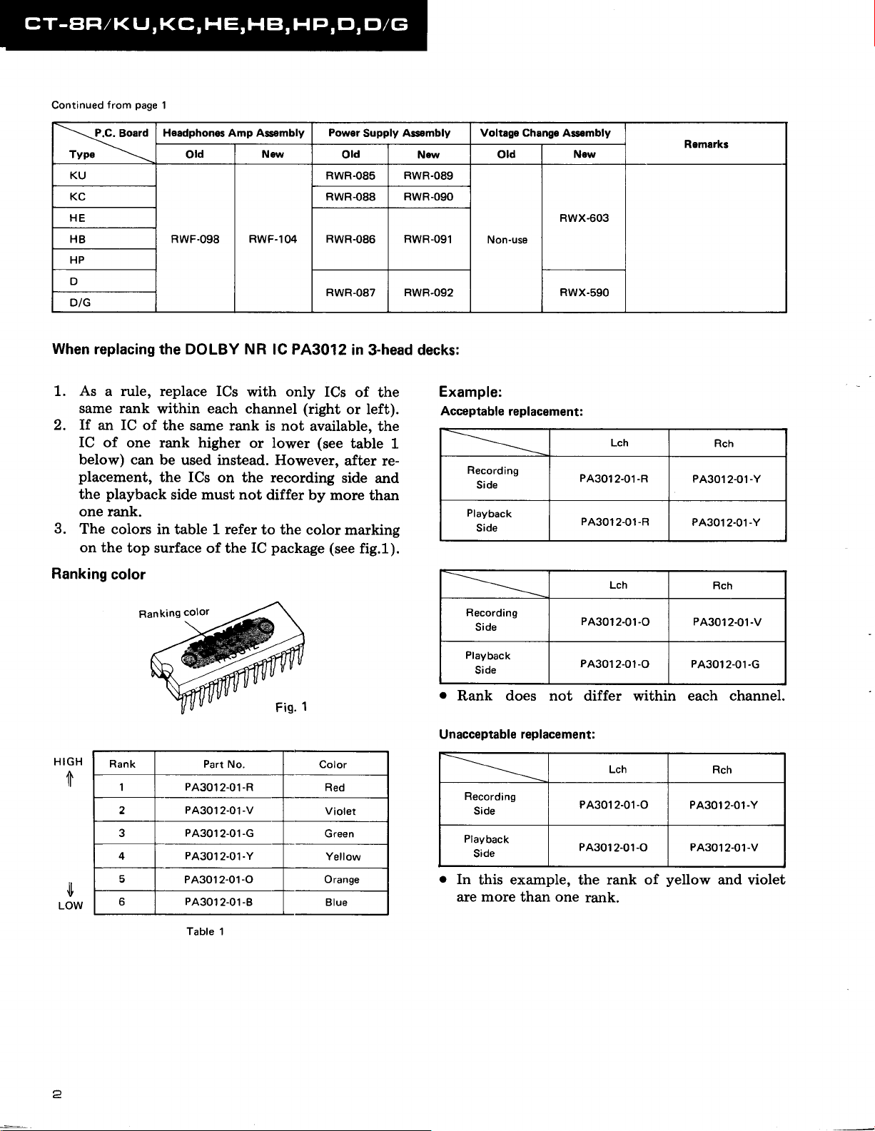
When
replacing the DOLBY NR
As
1.
2. If an IC
a rule, replace
same rank
of the same
within each channel
IC of one rank higher
below) can
placement,
the
one
3.
The
on the
playback
rank.
colors in table 1 refer
be used instead. However,
the ICs
side must not
top surface
old
ICs with only
rank is not
or lower
on the recording
of the
IC
Power
Now
old New old
RWR.O85
RWR-088
RWR.086
RWR-087 RWR.O92 RWX.59O
lC PA3012
ICs
(right
differ by more
to the
package
or left).
available, the
(see
after re-
side
color marking
(see
Supply
in
3-head
of
the
table
and
than
fig.1).
Assembly Voltago Change Assembly
New
RWR.O89
RWR.O9O
RWX.603
RWR-091HB
Non-use
decks:
Example:
Acceptable
1
replacement:
Recording
Side
Playback
Side
Lch
PA3012-O1-R
PA3012-01-R
Remarks
Rch
PA30't
2-01-Y
PA3012-01-Y
Ranking
HIGH
{t
tl
LOW
color
Rank
1
2
3
4
5
t) PA3012-01-B
Part No.
PA3012-01-R
PA3012-01-V
PA3012-01-G
PA3012-01-Y
PA3012-01-o
Table 1
Color
Red
Violel
Green
Yellow
Orange
Blue
Recording
Side
Playback
Side
Lch
PA3012-01-O
PA3012-01-O
Rch
PA3012-01-V
PA3012-01-G
Rank does not differ within each channel.
Unacceptable
Recording
Side
Playback
Side
o
In
this
are more
replacement:
example,
one
than
Lch
PA30't
PA3012-01-O PA3012-01-V
the
-o
2-0 t
rank of
yellow
Rch
PA3012-01-Y
and violet
rank.
Page 3
1.
PARTS
NO?ES;
c
When
ordering
the
follow
Ex.
1 When
and
56On
47ha 47x101
0.5a
la
Ex.
2 When
tors).
5.62ha
o
The
[.
safety
factor
designation.
o
your
For
**
and *-
**
GENERALLY
This
classification
number
resisfors,
ing examples.
there
47h ohm
56 x
0R5
010..
there
562 x
marh
found
of the
Parts
Stoch Control,
temperature,
,
shall be
LIST
convert resistance
first
are 2 effectiue
(tolerance
10t
.
.
are 3 effeetiue
100 5621.
on
some component
part.
Therefore,
MOVES FASTER
adjusted
humidity,
digits (any
is
shown by J
561
473..
digits
the
etc.
digit
=
.
.
SVo, and
.. RD%PS@AA,t
..... Rslp@tr@x
(such
as
.
. . RNZSR
parts
when
replacing,
mouing
fast
THAN *.
by each
items
distributor
values
into
apart
K
RD%PS
RN2H
in high
indicates
be
sure
are
because
code
0),
from
=
I0To).
E6m/
@Etri(
prickion
E6Emr
the
importance
to
use
indicated
it d,epends
form
such
metal
parts
with
as
shown in
as 560 ohm
resis-
film
of
identical
the
marhs
on model
the
of
Miscellaneous
P.C.
BOARD
Part
RWX.578
RWX-579
RWX.536
RWF-102
RWF-103
RWX.534
RWF.104
RWR-089
RWR-O9O
RWR.O91
RwR-092
RWS-152
RWX-603
RWX.59O
RWX-589
RWX.585
RXX-359
RXX-361
Parts
ASSEMBLIES
No.
List
Symbol
Mother
DOLBY
Equalizer
Sub
MIC
Meter
Headphones
Power
Function
Voltage
HE,
Reel
Capstan
Reel motor
(lncluded
assembly
drive coill.
Capstan motor
(lncluded
drive coil.)
Description
&
assembly
NR
assembly
amplifier
amplifier
drive
assembly
supply
(HE,
switch
change
HB
and HP
motor
control
motor
assembly
in the
C and
in
assembly
assembly
assembly
ampl if ier
assembly
assembly
control
coil assembly
the capstan motor
(KU
(KC
HB
and HP
(D
and D/G
assembly
assembly
typesl
(D
(KU,
and D/G types)
assemoly
assembly
C
reel motor
the
reel
typel
tYPe)
typesl
typesl
motor
KC,
D
drive
OTHERS
Mark Part
A
,A
**
A
A
A
**
F
*
RTT-231
RTT.263
RTT-251
RTT-252
RSA-O4g
RSA-052
RSA-043
RDG.O22
(RDG-030)
RDG-027
RDG-032
RDG.O29
RDG-024
RWX-234
RWX-235
c43-O03
REK-055
REK-064
REK-054
REK.O47
REK-051
REK.O63
RSX-045
RSX-020
No.
Symbol
Power
Power
AC
Spark
Fuse
Line Voltage
positions;
Description
&
transformer
l22OVl24OV; HE. HB, HP
U2OVl22OVl240V;
power
T2A
T800mA
T2.
T3.15A
TIA
T1.5A
(switchable
220V
switch
cord{KU,
killer
5A
22OV
t240Vl
(KU,
(HE,
{D.
(HE
(HB
(Hp
(D,
D/G types)
(KU
(KC
(D,
D/G
(KU,
(HE,
(HE,
{HE,
(D
typel
{D/G
Selector
l24OVl
positions;
3
(120V;
KU
(
1
20V; KC
D, D/G
KC
types)
HB.
HP types)
D/G
types}
KC
types}
tYPel
typel
type)
typel
tYPel
types)
KC
types)
HB, HP
typesl
HB,
HP
types)
HB,
HP
types}
type}
(Switchable
l2OVl
typel
type)
typesl
typesl
2
*
*
**
**
r
*
RAW-164
RAW-166
sLF-201C
RXX-337
RPB-095
RXP-l
11
RXX.334
Display
assembly
Level meter
Half
LED
Head
assembly
Erase
Head
Plunger
solenoid
FC
coil
assembly
assembly
J
Page 4
Mother
Assembly
CAPACITORS
Mark
Part
No.
CKDYF
CEA R1OM
CEA
CEA R47M
cEA
CEA 4R7M
CEA
cEA
ceA
cEA
473250
50
R22M
50
50
010M
50
50
3R3M
50
100M
25
220M
25
470M 25
(RWX-578)
Symbol
c301, c318,
O
c362
c327,
c325, C326,
c314, C355,
c371, C384
c329, C330
c31
3
c304, c374,
c303
& Dsscription
C335,
C328, C339,
C354,
C356,
C383
C363
C343
C357, C3&
C366
Mark
A
Part
No.
RsrPF
1olJ
RM 10-273J
RM11-103J
RM5-103J
RM5-223J
RM8-223J
BD74PM
trOO
J
SEMICONDUCTORS
Symbol & Description
R444
R397
R423
R424
R402
R463
R301-R332,
R350, R354,
R371-R377, R379-R381,
R385-R396, R399-R401,
R405-R421, R425-R443,
R446.
R464
R335, R337, R339-
R355, R364-R369,
R448-R451
R4g-R462,
,
R383,
R403,
R445,
cEA
cEA
cEA 220M
cEA
cEA222M
cEA470M
CEA
cEA
coMA 1 52J 50
coMA
coMA 332J
coMA
coMA
coMA
coMA
coMA
coMA
coMA
coMA
coMA
coMA
coMA
ccosL
CKDYF
cosH
coPA
RESISTORS
Note: When
into
Mark
Part
RCP-195
{RCP-1
RCP-189
{RCP-1451
RCP-'t96
(RCP-Is1)
101M
25
100M
16
16
221M 16
10
10
221M
6R3
10'tM 6R3
122J 50
50
682J 50
272J 50
272K
50
123J 50
103J 50
683K 50
123K 50
103K
50
473K
50
682K
50
472K 50
220K 50
1032
50
181K
50
182J 100
ordering resistors,
code
No.
50)
form,
and then
c365
c323, C324,
c386
c369
c302,
c345
c306, c322
c361
c360, c372
c346, C350
c342
c307,
c348, C352
c319, C320
c381, C382
c338, C349,
c309, c310
c336,
c340. c341
c312
c367
c31
5
c358
c378, C379
c305,
c316,
c31
1
conuert
rewrite
Symbol & Description
VR301,
fixed
VR302
VR303,
(33k-B)
C359,
c321, C368,
c308, c347,
C353
C337
c375,
C385
C31
7
resistance
the
part
the
VR3O5-VR307
(22k-Bl
Semi-fixed
VR304 Semi-f ixe d
C370, C377,
C376
C351
value
no. as
before
Semi-
(2.2k-B)
Mark Part
**
NJM4558D
(BA4s58)
(AN65521
**
PD6006
**
PD4012
**
PM3001
**
PA3010
**
PM9001A
**
pPD4011BC
**
TC4001BP
{HDl4001
{M884001
(pPD4001C)
**
84619
**
25C2497
(2SD1
**
2SD1189
l2SC2497l
(25D882)
**
2SC2060
(2SC2673)
(2SC1383NC)
**
2sA934
(2SA881)
**
2SC1740LN
cSC2021l
{2SC1815}
(2SC2634NC)
**
2SC1740LN
**
2SA1015
(2SA933LN)
(25A9371
(2SA1127NCl
*
1s2473
(us1040)
No.
189)
B)
BM}
Symbol &
Description
rc301
tc310
rc306
rc309
tc311
rc305
rc303, rc304
rc307
rc308
o301
0303, 0304
0302, 0306
0307
0305. o314-q|16,
0323, 0325,
o309-o31
0317,
D301-D305.
0326, 0328
2
0322,0324. 0327
D314-D336
O319-0321,
RCP-199
(RCP-1541
RCP-197
(RCP-152)
VR3O9
VR3OB
Semi-fixed
Semi-fixed
(1OOk-B)
(47k-B)
Page 5
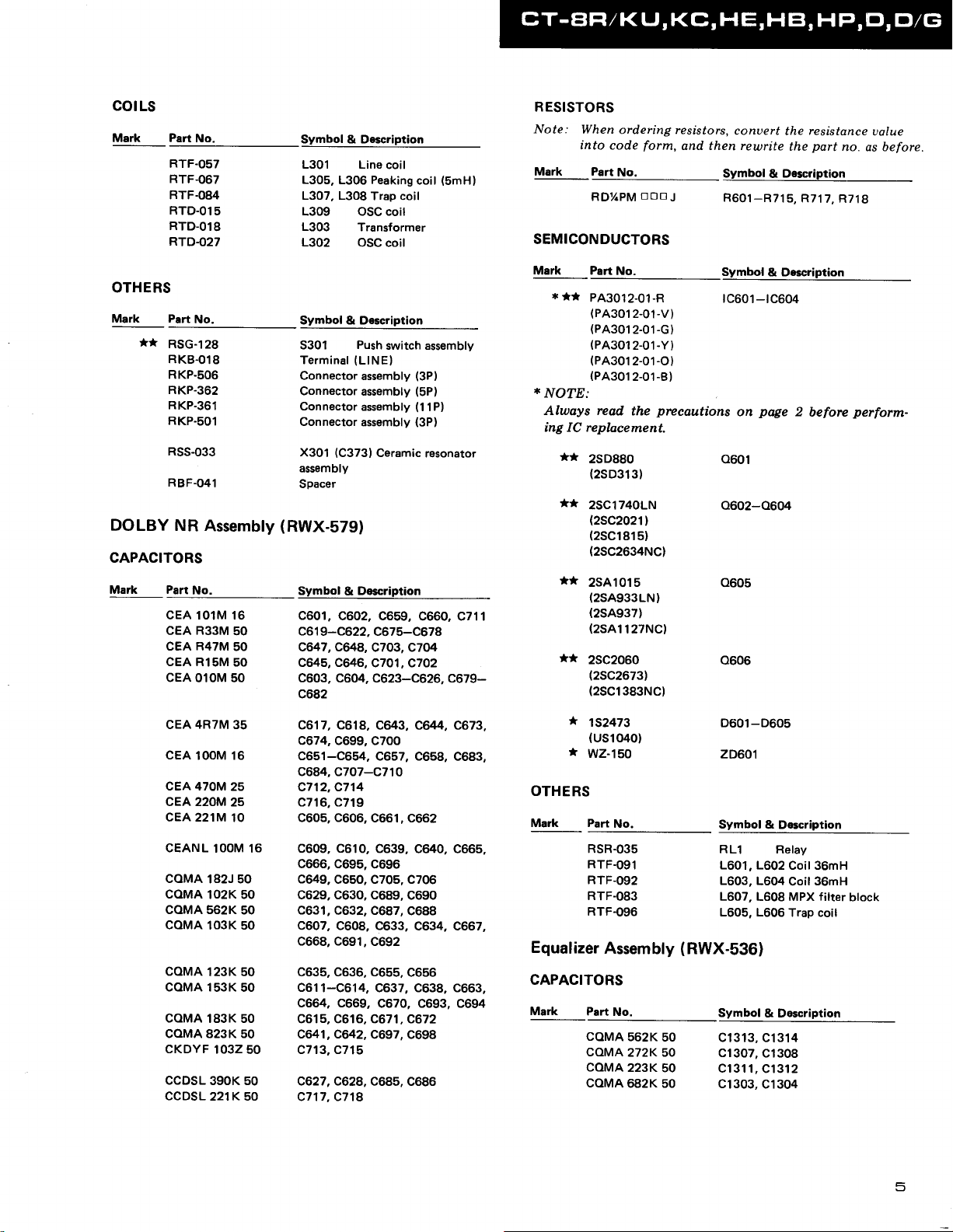
cotLs
Mark Part
RTF.O57
RTF-067
BTF-084
RTD.O15
RTD-o18
RTD.O27
No.
Symbol & Descraption
L301 Line
L305, L306
L307, L308
L309 OSC coil
L303
L302
coil
Peaking
coil
Trap coil
Transformer
OSC coil
(5mHl
RESISTORS
Note:
When
ordering resistors,
into
code
form,
Mark Part
No.
RD7.PM
DOtr
J
SEMICONDUCTORS
and then rewrite
conuert
Symbol & Description
R601-R715,
resistance
the
part
the
R717,
uolue
no. as before
R718
OTHERS
Mark Part
**
DOLBY
CAPACITORS
Mark Part
No.
RSG-128
RKB.O18
RKP.5O6
RKP.362
RKP.361
RKP-501
RSS-033
RBF.O41
NR
No.
cEA 101M 16
CEA R33M
CEA R47M
CEA Rl5M
cEA
CEA
cEA
cEA 470M
9EA220M25
cEA 221M
CEANL
coMA
coMA
coMA 562K
coMA
coMA
coMA 153K
coMA
coMA 823K s0
CKDYF
ccDsL
ccDSL
Assembly
50
50
50
010M 50
4R7M
35
100M 16
25
10
1OOM 16
182J 50
102K 50
50
103K 50
123K 50
50
183K 50
103250
390K 50
221K50
Symbol & Description
5301
Terminal
Connector
Connector
Connector
Connector
X301
assembly
Spacer
Push
(LlNEl
assembly
assembly
assembly
assembly
(C3731
switch assembly
Ceramic
{RWX-579)
Symbol & Doscriptaon
c601,
c602. c659,
c619-C622,
cil7,c&a,c703,c1M
c64s, c646,
c603,
c682
C617, C618,
c674, C699, C700
c6s1-c654,
c684, C707-C710
c712, C714
c716, C719
c605, c606,
c609,
c666, C695,
c649,
c629, C630. C689,
c631,
c607, c608, c633,
c668, C691,
c635, C636, C655,
c611-C614,
c664, C669,
c61s, c616, C671,C672
c641,C642,
c713, C715
c627,C628,
c717, C718
C675-C678
C701, C702
c604, c623-C626, C679-
C643, C6,r4, C673,
C657, C658,
c661, C662
c610,
c639,
C696
C650, C70s, C706
C632, C687,
C692
C637, C638, C663.
C670. C693, C694
C697, C698
C685, C686
(3Pl
(5P)
(1
1P)
(3P)
resonator
C660, C711
C683,
C640, C665,
C690
C688
C634. C667,
C656
Mark Part
r,**
*
NOTE:
Always read
No.
PA3012-01-R
(PA3012-01-v)
(PA3012-01-c)
(PA3012-01-Y)
(PA3012-01-O)
{PA3012-01-B}
the
ing IC replacement.
**
2SD880
{2SD313}
**
2sc174oLN
(25C2021
(2SC18151
(25C2634NCl
**
2SA1015
(2SA933LNl
(2SA9371
(2SA1
127NCl
**
2SC2060
(25C26731
(2SC1383NC)
*
1s2473
(us1o40)
*
wz-150
OTHERS
Mark Part
Equalizer
No.
RSR.O35
RTF.Og1
RTF-092
RTF.O83
RTF.096
Assembly
CAPACITORS
Mark
Part
No.
coMA
coMA
coMA
coMA
562K
272K 50
223K
682K 50
precautions
)
(RWX-5361
50
50
Symbol
& Description
1c601-tc604
page
on
0601
0602-0604
0605
0606
D601-D605
2D601
Symbol
& Description
R
Ll Relay
L601, L602
L603,
L607,
L605, L606
Symbol
cl313,
c1307,
cl31 1,
cl303,
Coil 36mH
L6O4
Coil
L608 MPX
Trap coil
& Description
Cl314
C1308
C1312
C1304
2
before
36mH
filter
perform-
block
5
Page 6
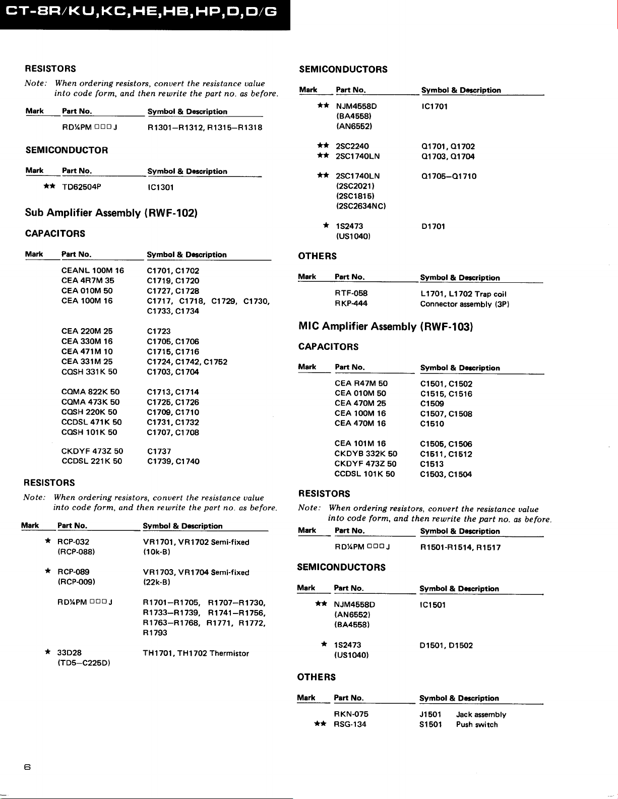
RESISTORS
Note: When
ordering resistors,
into code
Part
RD]/4PM
form,
No.
DtrD
SEMICONDUCTOR
Mark Part
**
Sub Amplifier
No.
TD625o4P
Assembly
CAPACITORS
and then rewrite
J
conuert the resistance ualue
Svmbol & Description
R1301-R1312, R131
Symbol
tc1301
(RWF-I02)
part
the
& Description
no.
as before.
5-R131 I
SEMICONDUCTORS
Mark Part
**
**
**
No.
NJM4558D
(8445581
(AN65521
25C2240
2SC1 740LN
2sct74oLN
{p.SC2021l
(2SC181s)
(25C2634NC)
*
152473
(us1040)
Symbol & Deccription
rcl701
01701, 01702
01703, 017(M
01706-01 710
D1
701
Mark Part
CEANL 1OOM 16
CEA 4R7M
cEA 010M
cEA 100M 16
cEA220M25
cEA 330M
cEA 471M
cEA 331M 25
cosH
coMA 822K 50
coMA 473K 50
cosH 220K
ccDsL 471 K
cosH
CKDYF 473250
ccDsL
RESISTORS
Note: When
into code
Mark Part
RCP-032
(RCP-088)
RCP-089
{RCP-009)
RD74PM
33D28
(TDs-C225Dl
No.
35
50
16
10
331 K 50
50
50
101K 50
221K50
ordering resistors,
No.
and then rewrite
form,
DtrO
J
Symbol & Description
c1701, C1702
c1719,
C1720
c1727, C1728
c1717, C1718, C1729,
c1733, C1734
c1723
705, cl 706
cl
cl715.
Cl716
c1724, C1742,
cl 703,
c1713, C1714
c1726, C1726
cl709,
c1731,C1732
c1707,
cI737
c1739, C1740
conuert the
Symbol & Description
VRl
701, VRI
(10k-B)
VRI
703, VR1 7@
l22k-Bl
R1701-R1705,
R1733-R1739.
Rl763-R1768,
Rl793
TH1701,
C1752
Cl 704
Cl710
Cl708
resistance
part
the
f H17O2 Thermistor
no. as before.
702
Semi-fixed
Semi-fixed
R1707-R1730,
R1741-R1756,
R1771, R1772,
Cl730,
ualue
OTHERS
Mark Part
MIC
CAPACITORS
Mark
RESISTORS
Note:
No.
RTF-058
RKP444
Amplifier
Part
No.
CEA R47M
cEA
010M
cEA 470M
cEA
100M 16
cEA 470M
cEA 101M
CKDYB
CKDYF 473250
ccDsL
When
into
Part
RDy.PM
332K 50
101 K 50
ordering reslsfors,
code
No.
Assembly
50
50
25
16
16
and
form,
ootr
J
SEMICONDUCTORS
Mark Part
**
*
No.
NJM4558D
(AN65521
(8A4558)
1s2473
(us10401
OTHERS
Symbol
& Deccription
L17O1
L17O2
,
Connector
assembly
(RWF-103)
Symbol
& Dercription
cl
501, Cl 502
c1515,
C1516
cl509
cl507. Cl508
c1510
cl505,
Cl506
cl511,
Cl512
cl513
cl
503, Cl 504
conuert
then rewrite
Symbol & Dercription
R1501-R1514,
Symbol & Detcription
rc1501
Dl501, Dl502
the resistance
the
Trap coil
(3P)
part
no.
R1517
ualue
as before.
**
Part
No.
RKN-O75
RSG-134
Symbol & Description
J15O1
51501
Jack
Push
assembly
switch
Page 7
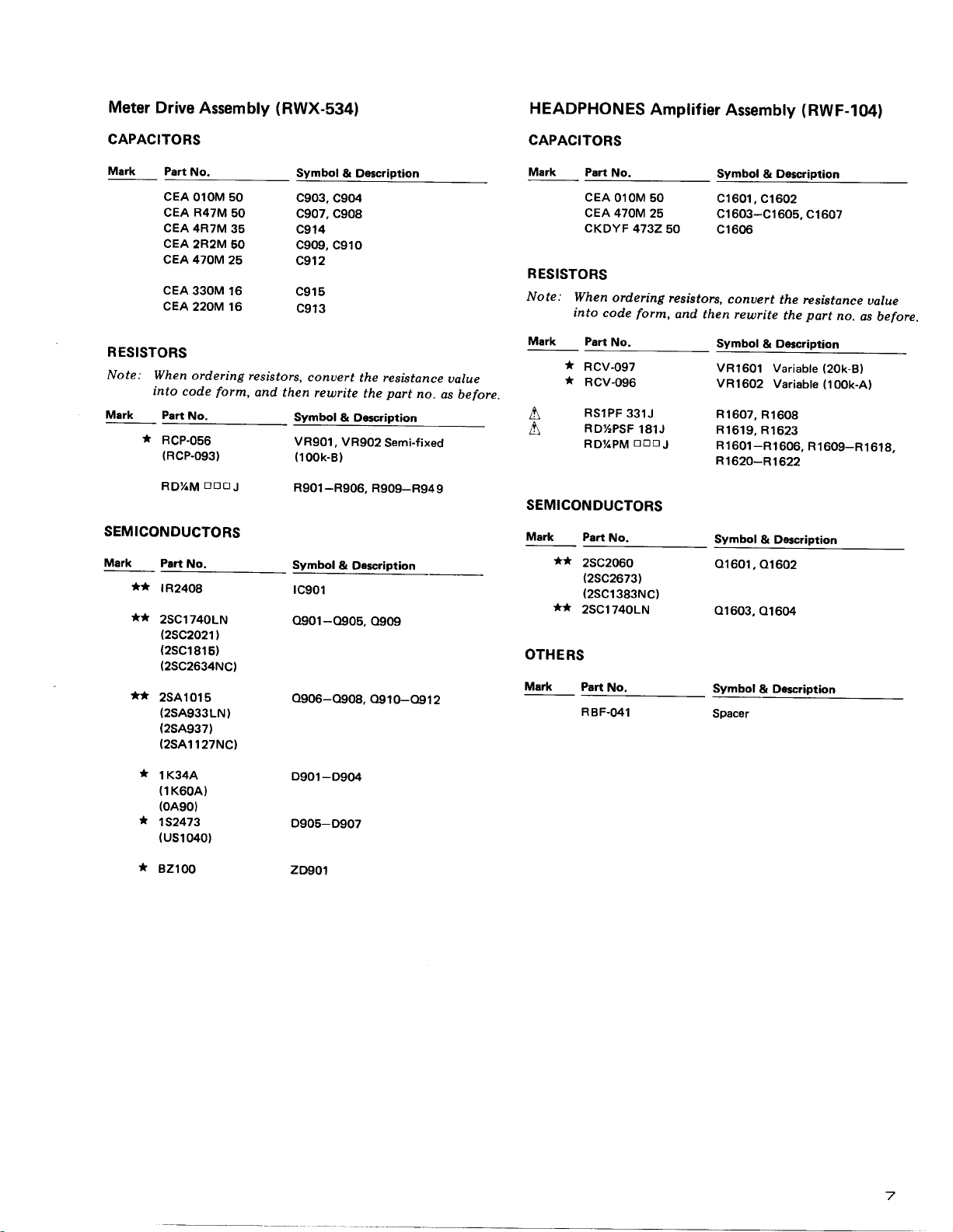
Meter
Drive
Assembly
(RWX-534)
HEADPHONES
Amplifier
Assembly
(RWF-104)
CAPACITORS
Mark
RESISTORS
Note:
Mark Part
Part
cEA
cEA R47M
cEA
cEA
cEA470M
cEA
CEA
When
into
code
No.
r
RCP-056
(RCP-Og3)
RD7.M
No.
010M 50
50
4R7M
35
2R2M
50
25
330M
16
220M 16
ordering
form,
oooJ
SEMICONDUCTORS
Mark
Part
**
tR2408
**
2sc174oLN
(2SC2021
(2SC1816)
(25C2634NC)
**
2SA1015
(2SA933LN)
(2SA937)
(2SA1
No.
l
127NC)
Symbol
C903,
C907, C908
C914
C909,
C912
C915
C9t3
resistors,
and
then
Symbol
VR9O1,
{100k-B}
R901-R906,
Symbol
rc901
ogot-o905,
0906-0908,
& Description
C904
C910
conuert
rewrite
& Doscription
VRg02
& Description
the resistance
part
the
no.
Semi-fixed
R9O9-R949
o9o9
O91o_O912
ualue
as
before.
CAPACITORS
Mark
RESISTORS
Note:
Mark
A
A
Part
No.
cEA
010M 50
cEA 470M
CKDYF 473250
When
ordering
into
code
Part
No.
*
RCV-097
*
RCV-O96
RslpF
331J
RD%psF
RD%PMotroJ
25
form,
181J
SEMICONDUCTORS
Mark
Part
**
2SC2060
{2SC2673)
(25C1383NC)
**
2SC1740LN
No.
OTHERS
Mark
Part
No.
RBF-041
Symbol & Description
C1601.
C1602
Cl603_C1605,
C1606
resistors,
and
conuert
then rewrite
Symbol
vR16o1
VR16O2
R16o7,
R1619,
R1601_Rl606,R1609_R1618,
R1620-R1622
Symbol
01601,
01603,
01604
Symbol
&
Spacer
Cl607
the resistance
part
the
Detcription
&
Variabte
Variabte
R16og
R1623
& Description
01602
Description
ualue
no.
as
(2ok-Bl
(lOOk-A)
before.
*
1K34A
(1K60A)
(oA90l
*
1s2423
(us10401
*
82100
D901-D904
D905-D907
2D/901
7
Page 8

Power
Supply Assembly
CAPACITORS
Mark Part
No,
cEA222M25
cEA222M50
CEA
0EA221M25
cEA 331M 25
cEA 101M 16
cEA 101M
cEA 220M 16
CKDYF 1032 50
RESISTORS
Note: When
into code
4R7M 35
10
ordering
form,
(RWR-089;
(RWR-090;
(RWR-091;
(RWR-092;
Symbol & Description
c1201, C1202
cl203
c1217
c1213
cl206
cl205
c1211, C1212
c1204
cl
c1219
resistors,
and
conuert the resistance
then
KU),
KG),
HB, HE
D
and D/G)
208-C1 21 0, C121
rewrite
the
part
HP),
and
4-C1216,
uolue
no. as before
A
A
A
A
A
Part No, Symbol & Description
740LN
2SC1
l2sc2021l
(2SC1815)
(2SC2634NCl
2SA933LN
(25A937)
(2SA10151
(2SA1127NC)
2SC1740LN
l2sc2240l
WO3B
01207, O1208
41202,
01206
01205, 01209
01201, D1202
(w03c)
t
S2VBlOF
*
152473
D1204
D1203,
D120,9-D1211
(us1040)
RD3.OE82
(x2031)
RD5.6E82
2D1201
2D1202
(wz-0s6)
RD4.7E82
ZD12M
lwz-u4l
Mark
A
A
A
A
Part
No.
RSlPF
6R8J
RS%PSF
RS%PSF
RDY.PM
RDz.PM
trtrO
otrtr
101J
271J
J
J
SEMICONDUCTORS
Mark Part
a**
A**
The Power
Assembly
Mark
A
No.
25D880
(2SD313)
258772
(2SA1096)
Supply
(RWR-089)
Symbol & Description
R1211 Resistor
R1221 Resistor
Spacer
Fuse
Fuse holder
Symbol & Description
Rl221
R1202
Rl
205
R1201, R1
R1
21 3.
R120,
R1215-R1
R1222,
Symbol & Description
41201,
01203
Assembly
except
holder
for following
C
B
(KU
type)
R1207-R1
203,
R1214, R1218, R1224
R1206, R1211, R1212,
R1219, R1220.
217,
R1223, R1225
01204
210,
(RWR-090) (RWR-091)
sections.
typo
KU
(RWRO89l
RO%PM822J
RSlPF
6R8J
RBF.O41
used
Be
RD'I/.PM
*
A
RDloEB3
(wz-1001
*
wz-085
(RD8.2E92I
(RD8.2E83l
OTHERS
Mark Part
RBF-041
REE-051
RKH.OOS
R8A-026
RKP.366
RKP.475
(RWR-092)
and
type
KC
(RWR-0901
682J
used
Be
No,
Part No.
2o1203
2o1205
Symbol &
Spacer
Insu lator
I nsu lator
Special screw
Connector assembly
Connector assembly
Fuse holder C
Fuse holder
the
are
HE. HB, HP typo
(RWR.()91l
RDTIPM
same as
682J
Be used
D$cription
(KU
type)
B
the
D, D/G types
(RWR{r921
RDZIPM
(7P)
(3P)
(KU
and KC
(HE,
HB and HP types)
Power
Supply
682J
types)
a
Page 9
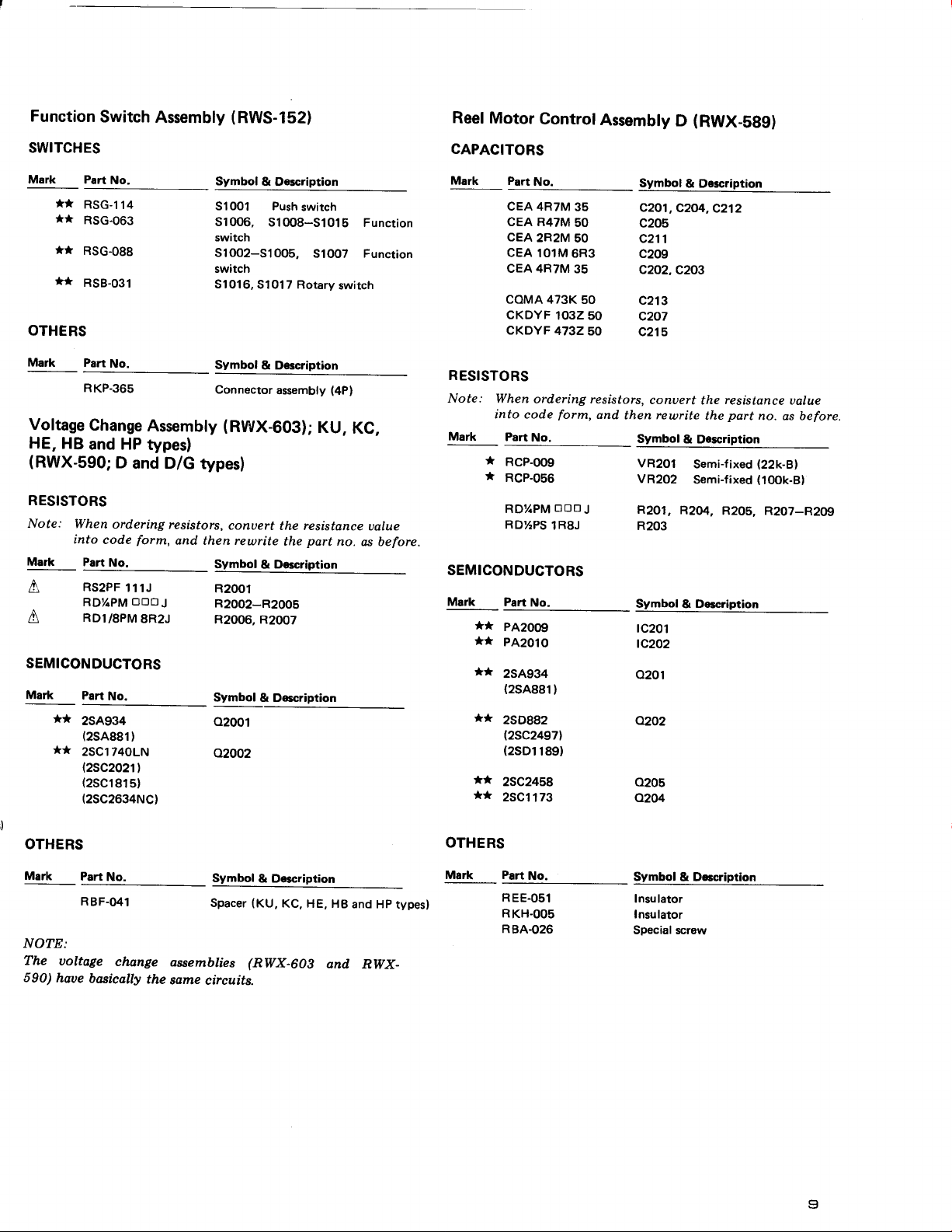
Function
SWITCHES
Switch
Assembly
(
RWS-152)
Reel Motor
CAPACITORS
ControlAssembly
D
{RWX-Sgg)
Mark
**
**
**
**
Part
No.
RSG_I14
RSG-063
RSG-088
RSB-031
OTHERS
Ma*
Voltage
HE,
(RWX-590;
RESISTORS
Note:
Mark
A
A
SEMICONDUCTORS
Mark
Part
No.
RKP-365
Change
HB
and HP
When
ord,ering
into
code
Part
No.
RS2PF
RDy4PM
RDI/8PM
Part
No.
2SA934
(2SA881)
2SC1 740LN
l2SC2021l
(2SC1815)
(2SC2634NC)
Assembly
types)
D
and D/G
form,
111J
OOO
8R2J
J
Symbol
& Description
SIOO1 Push
s1006,
switch
sloo2-s1005,
switch
51016,
51017 Rotary
Symbol
& Description
Connector
(RWX-GO3);
types)
resistors,
and then rewrite
conuert
Symbol & Description
R2001
R2002-R2005
R2006, R2007
Symbol
& Doscription
02001
02002
switch
s1008-s1015
sl007
switch
assembly
(4pl
KU,
the resistance
part
the
no.
Function
Function
KC,
ualue
as before.
Mark Part
RESISTORS
Note:
Mark
i
*
SEMICONDUCTORS
Mark
**
**
**
No.
CEA 4R7M
CEA R47M
CEA
2R2M
CEA
101M
CEA 4R7M
coMA 473K
CKDYF
CKDYF
When
into code
Part
RCP-009
RCP-056
RDz.PM
RD%PS
Part
1032 50
47325,0
ordering resisfors,
form,
No.
trtrO
1R8J
No.
PA2009
PA2010
2sA934
{25A881}
25D882
l2sc2497l
(2SD1189)
**
2SC24s8
**
2SCl
173
35
50
50
6R3
35
50
J
Symbol
c201,
c205
c211
c209
c202,
c213
c207
c215
and
conuert
then rewrite
Symbol
VR201
VR202
R201,
R203
Symbol & Description
tc201
tc202
o201
0202
o205
0204
& Description
c204,
c212
c203
resistance
the
part
the
& Description
Semi-fixed
Semi-fixed
R204,
R205, R207-R209
ualue
no. as before
l22k-Bl
(100k-Bl
OTHERS
Mark
NOTE:
The
uoltage
590)
haue
Part
No.
RBF-(M1
change
basically
assemblies
the
same
Symbol
Spacer
circuits.
& D$cription
KC, HE, HB
{KU,
(RWX-6O|
and HP
and RWX-
types)
OTHERS
Mark Part
REE.Os1
RKH-OOs
R84.026
No.
Symbol
Special screw
& Dcccription
Insu lator
Insulator
I
Page 10
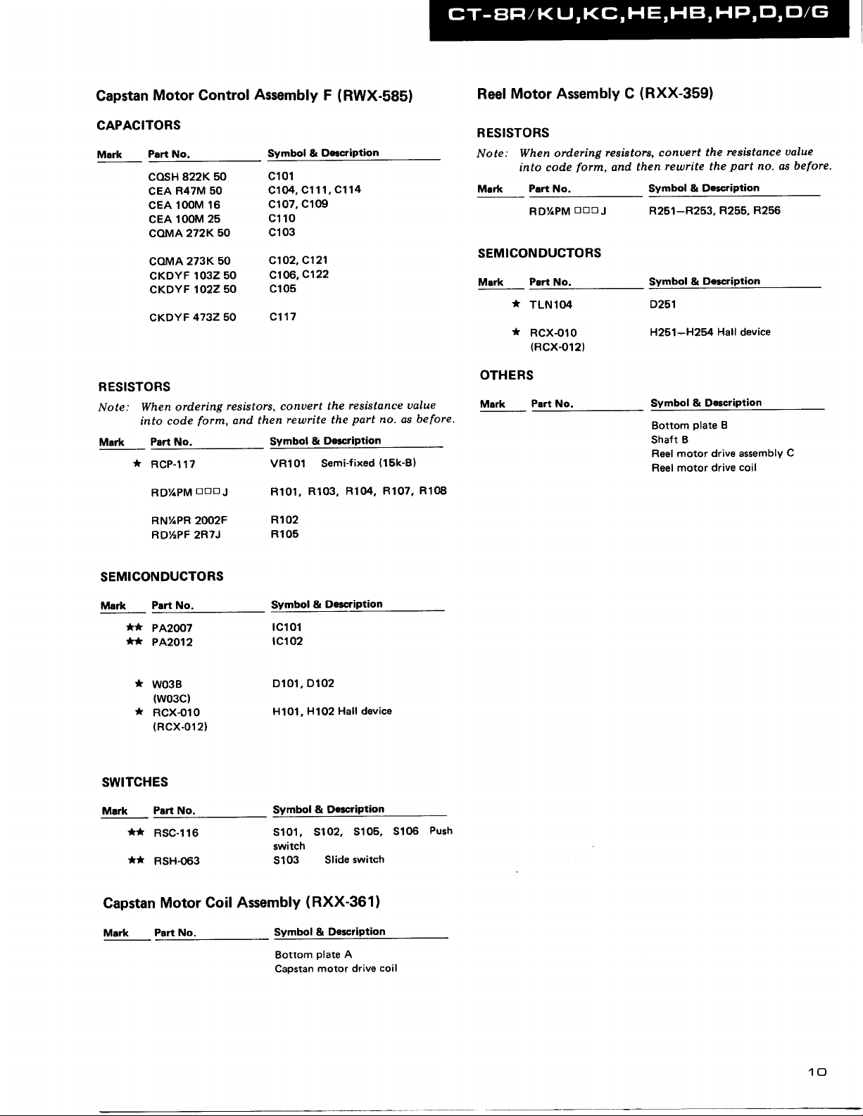
Gapstan
Motor Control
Assembly
(RWX-585)
F
Reel
Motor
Assembly
C
(RXX-359)
CAPACITORS
Mark
Part No,
cosH
CEA
cEA 100M
cEA
coMA
coMA
CKDYF
CKDYF 102250
CKDYF
RESISTOBS
Mark
When
into code
Part No.
*
RcP-117
RDYIPM
RN%PR
RDY2PF 2R7J
Note:
50
822K
R47M 50
16
25
100M
272K
273K
1032
473250
ordering
form,
Dtrtr
2OO2F
Symbol &
c101
cl04,cl11,C114
c107,
cl
10
50
50
50
cl03
c102,c121
c106.c122
cl05
c117
resistors, conuert
and then
J
rewrite the
Symbol
VR101
R101,
R102
R105
Deccription
cl09
resistance
the
part
Dercription
&
Semi-fixed
R103. R104,
ualue
no. as
(1sk-Bl
R107,
before'
R108
RESISTORS
When ordering
Note:
Mark
into code
Part
RD%PM
form,
No.
DODJ
SEMICONDUCTORS
Mark
Prrt
*
TLN1o4
*
RCX-010
No.
(RCX-o121
OTHERS
Mark
Part No.
resistors, conuert
rewrite the
then
and
& Dcscription
Symbol
R251-R253,
&
Symbol
D251
H251-H254
& De*ription
Symbol
plate
Bottom
B
Shaft
motor drive assembly
Reel
motor drive
Reel
resistance
the
part
R255,
Delcription
Hall
device
B
coil
no. as
R256
value
before.
C
SEMICONDUCTORS
**
fr
Part No.
PA2007
PA2O12
Mark
w03B
(w03c)
RCX-010
(RCX-012)
swtTcHEs
Mark
Capstan
Mark
Part No.
**
RSC-116
**
RSH-O63
Motor Goil
Part No.
Symbol
rcl01
rc102
Dl01,
H101, H102
Symbol
s101, sl02,
switch
5103
Assembly
Symbol &
Bottom
Caostan
Decctiption
&
D102
Hall device
& Description
sl05,
switch
Slide
(
RXX-361
Description
plate
A
motor drive
)
coil
sl06
Push
10
Page 11
3
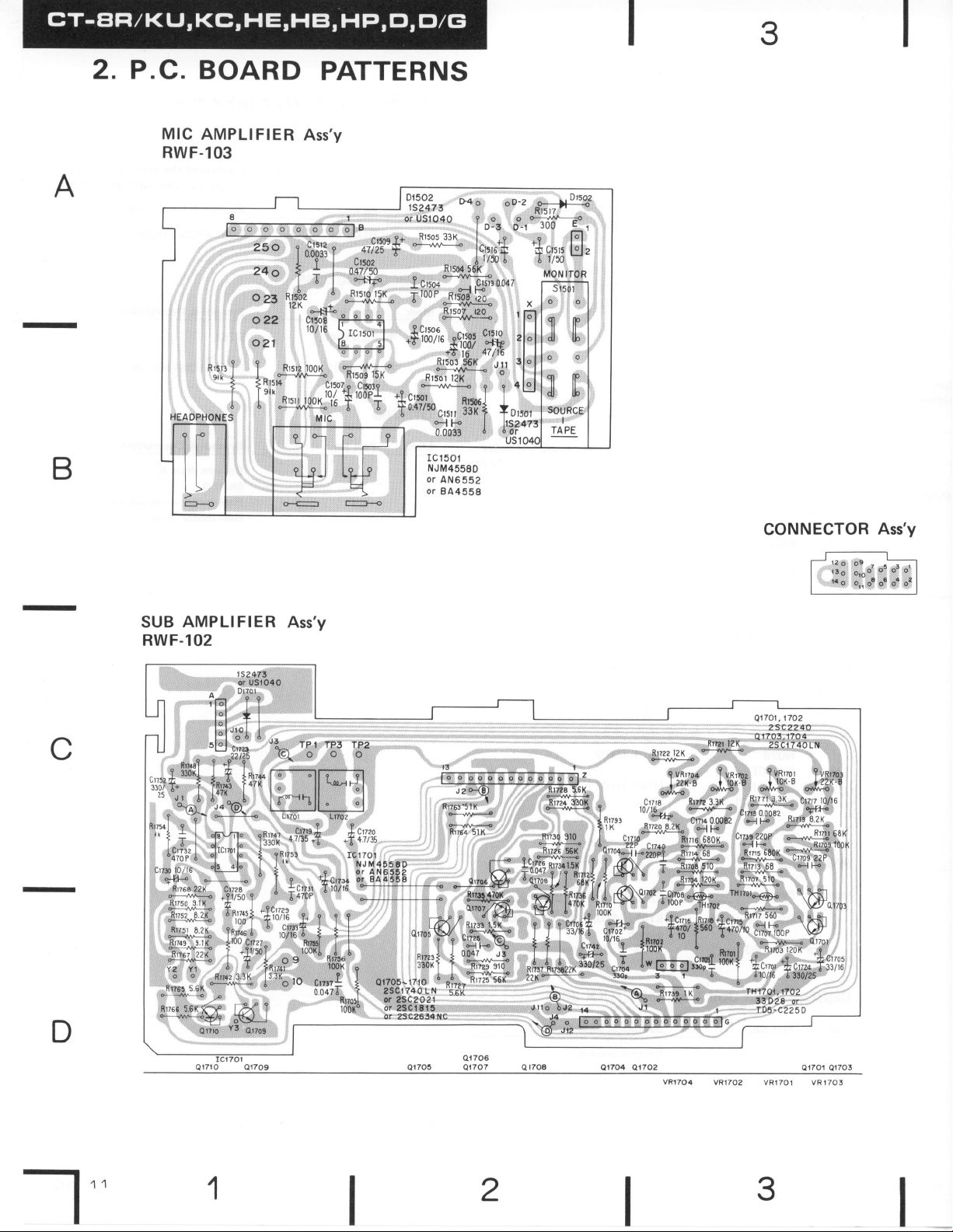
2. P.C.
A
B
BOARD
MIC
AMPLIFIER
RWF-103
PATTERNS
Ass'y
AMPLIFIER
SUB
RWF-102
Ass'y
CONNECTOR
Ass'y
D
-l"
1
2
vR1702 VR1701
3
VRr703
t_
Page 12
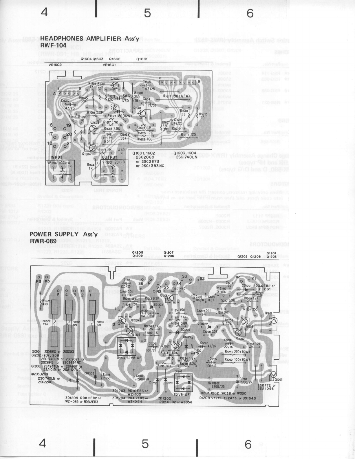
4
5
6
HEADPHONES
AMPLIFIER Ass'y
RWF.104
Q.r6O4
Q16O3
Qr6O2
Ql6Ol
Q160t,1602
25C2060
or 25C2673
or
2scl 383 Nc
Q1603,1604
2SC|740LN
POWER
SUPPLY Ass'y
RWR-089
zDl205
RDt.zE82
or?or
Qr2O1
Qt?o3
qr2o2
o;
Page 13

7
f
B
I
MOTHER
RWX-578
i:iii:*ist1*:",
l-iilii&r*,.lr
:;frffi;,t"i--
qsi#ii.rii,r,,
fii,![3,'.,i"?'**.'
*4
Ass'y
Q323
Q319
eeo?o.r
^"
I
m!,*";
;
ICaO5
ICrOt
Q3?O
Q326
r001'7
*
IC3O6
Q3lO
fP4
TP6
Ulu
,fi
F***rli%,,s!
r,';ff
lil"
H|;*{'.i,4td;iTii;{-ilffi,ffi-1,,,.^,^,fb,iif{lL,r**,,.u{i...
",",$i"ll'#lJT'r
lil**11fthffi$f
'l$Sg
*#Affi'H:#;-}$Trnn'-"_'?^''*,i'*;ttf-i-iii,i"''1;:
IC311
Q3O9
rP1 VR305
vR306 VRS9
Q312 Q31r
Es*
*
J+*
IC307 IC30a
Q32?
\ )
Y"
IC309
IC3IO
Q321
*!H:ll::$,:iio
**=a"
Ql23
q34
S5ffi
ffipg#-trffi,H,'q_=,.,
-,*-''*'
*.r-=-
,,n*r
"\lIlJ"Jl
i
'
m
--::
&irfrrr
#*{ t{ t--i?i3t*-*g
;\I.:L'.*H
"
i-1,=- u
Tu
*i#il
#*
of
f ll.@t\--F1 Iro I
lk
ll
-J
=-
i
"{}-
clzb'o.oozz
o !-$*n I
f;lr .,^-_.o |
**r
"
"["]
fir-
"+$'J
lolr
?ryrlT'Ii;u1.*,,,$*l,fiar't
L^ ]
dajt
11 I :',,",t,,,1;.,ru,@ *1,,i.
33x'8
f,
*",'!fii,','ffi
1,,,
i"
"
"&
#
"loro...o.
2sc?o6o
or
I
2scr383[c
f
ono'zsczett -
IC3O3,3O4
q3r7
Q3O6
r z-T\ lpo ^^-.
O3O7
Q3O5 Q3O4 Q3O3 O3O2
Q327 Q3?A
o'?to"le.
ffi,|,*'i,@[ig""i6'
*l#.$?}
,s,u"s'il
;;,
u"
u
[ ffig?#i
u.ur
ur5rwP/"1J-\
.-*(
ctrziooe$\*,/
i,*Plul I,,*
gF.l
ooor^.r:3::.
I ,e
i t
^cris.
00068
t's'
i"
circ
'/50
W.#5ffifrffiffiU*r
Milsr*u,,;.,,,,r,-,.",euu,dli
81fu,,,.ffi,""rfu
#,#f
P040lZ
,ffir*"1i
lCao6
tJ:--.---*r
,,**ffi
Ht
-nf
.,..
*l- l;17
n, ,
lJefl'ml
;"#fl"*ili
.i*,fl",'#;::
',
J"'11,
o'tl$*--o-.
lffi'I*-.*;14:**-'
"%';*gi'ffi';,,fr;il;c;
i l"l,
l" ^.!9ir,-l II
*iii_
q'-#
F'l lrl
J,o
%f*
B''d*
?l ,'$
-{
Tqyllf
P"
t UXll*i-ETi,#:lll .l[,,,,,.*,,",*,.,,r.JH
t
ll:t?,s
Es2tfir
r {iff
F\ +*-. {*l i**jt, li*r-iL#*e6
t.....
llR
.
--r@.iK*
-
TTI ITI
tlll,"
B"
I r*i
"
I i {,_rl
"
T-..q++.;-"g"YigH"ifi.-
rp."*i-g-+llt
,";tfl1
.
l.--*"jh
l-@-*
*r#'
Jrl:i
'uo_".
l:l'" ll
lrl
ll,*.ns,,
ffii"-----lfilil
-
rl*.
6;;o.*1
,+--+--J
""
,,
r]{*,m-1".'.i'^-,,'-
,.,",dn":*l
,.,",st',":-l
,*pl
lzx
J
_-- |
lr-m"-ffi'.'frfrffi*
r+ii*s44+-
fil**uii
xBRssrB"'
-,rl
*r
:#
iHllj
JH'
i*.
ikl
t
Jd
_ffi"_\h
-*--
'rc"*
iuqoo, - 1 --=+.--- *R!r3
"iil'Eo*I
ff
ti|;l ffiJT'J
''
*
#
lil
t'
'i""*4
Y"rul]'
**16
Jr*
l^*ffi*[
ffi lone
i;,,ry
Tffir
Sf;116*'lPI
po6oo6
rca'
ICaE
l)
=msffi:t-'l
+Tili.
PD6OO6
l;SE
*ru,,
Fo__E
YF(4
l'*##
^ ;" I l'1" ,-+r
6
iJ"e_
m:,:'
ll
"'[,ffi",,ffi
"---'------*
E
:--
t'-
]
I
+T:
,*rffo'',
*-Y'J
ffii',-
lu*
= -,-^ +.#"
-i
I
;--r
J'r'
lii,,:"';.''r,'^.,
rl *,'*^, l.s biuol.lttt
TF
+
:r{:x{ .]_
,*i
"'l',.A\*f)
Ras5t5OK-
^-,,,yi
1ffi'*S:*
"'^
"
Lq\ X.-^
C*t,"
ll
#ffia-
t I
I,'
*ttFrLrERDoLayilR
|f.l Fl ffi]
'
Jr.,fll1,Jlr*gl_--
-, u,'0,
|
DoLBvNR
*,
+-'
I
7
B
lo o o o a a
O o o o o o o
O O I
I
t_
Page 14

10
11
12
1
CONNECTOR Ass'y
ffi*-rn
EOUALIZER
RWX-536
Ass'Y
A
B
FUNCTION
(RWS-1521
SWITCH Ass'y
I
D
I
10
L
Page 15

1
2
3
A
DOLBY
RWX-579
NR
Ass'y
Q6Or
IC6O4
Q6O4 Q6O6
Q6O5
Q6O3
IC6O3
Q6O2
IC60i
IC602
D
1
32
Page 16

r'
4
5
6
CAPSTAN
RWX-585
MOTOR
CONTROL
Ass'y F
VOLTAGE
RWX-603
GHANGE Ass'y
4
65
L
Page 17

REEL
RXX-359
MOTOR
I
Ass'y C
I
10
REEL N
RWX-58
METER DRIVE Ass'y
RWX-534
O9ll
Q9l2 IC'OI
Q906
Q902
q9Oi
8 10
I
Page 18

10
REEL
RWX-589
MOTOR
IC20t
CONTROL Ass'y D
Q2040205
Q20t o2o2
A
B
t_
10
11
12
Page 19

3.
SCHEMATIC
SIGNAL SECTION
@
@
o
(9
DIAGRAM
DOLBY Ass'y R\flX- 579
|--:
I
rc60l
REC IA
IN
t23
F'PAss
3
P8
SW VCR
-i
ril
REF.
GNO
4
SCF
-{
Yr
-2 -3
PilS€
sw
REc
ouT
a
corT a.s
scF
-2
t7
vcF
HPA
-2
-2
f2 ss ss
-2 -2 -l
2t 22 2:
-
lc6ola
:
604
ftI RELAY
0605,606:
RELAY
-
RSR
ORIVE
O35
P.8
IA
SYPASS GilOtx
SW
-r
rx
R€F.
scF
OOLEY
iIR
(
C TYPE}
8A
TI
-2
PHASE
a
REC
coflT A.s
ouT
E
H
E
IEC
SU
A
-t
wT coxT.
t3la{tt6t?t8€
scF
-2 -2
318|9A2l
SCF VCR HPA
-2 -2 -2
a.s
Lt*f-lt*-"
HP f2 12
vcR
-2
rr
LY
't
jrrF
-t
reoe
I
f2 f2
- | -2
&21
-2
LC@
36d
R640
tl
-
0.6
ss
ss
-2 -(
e2:
-
I c60a
REC IA
rr an$s
t23
HPA
vtr
-l
Gm
SCF
789tOitt2t3t4
Sw
-t -? -t
ll ll St
-2 -3
BASE
REc
OUf
a
coffi
SCF VCF HPI
-2
a.s
tTlgD
16
-2 -2
-
k : kn,
p : pF
im-
swrTcHEs
:CASSETTE
SlOl
slo2 : ERASE PREVENT
SIO3: FWO/REV
SIO5:
5106:
S3O2:
s303:
Th.
Thir i3 the
to imprqmmts
due
H/qUr
SELECTOR
AUTO
TAPE SELECTOR NORM
AUTO TAPE
SELECTOR METAL-CrO2
POWER
couNlER
undrlimd indicotos
basic $hmatic
in d6ign.
OETEG|OR NO HALF - HALF
o€1ECTOR
th. lwitch
diagram,
ru'
FWD- REV
ON _ OFF
ON _ OFF
rositim.
the aturl ciBit
bnt
-
-HIGH
fiOLE
NO
may vary
3
1
in tr, %W,
lndicared
M : Mf,l,
{F)
2. CAPACITORS:
Indicared in
Indication
3. VOLTAGE
r DC voltage
I
4. OTHERS:
Signal
+:
:
Adiuning
A
mark tdnd
The
I
poname
ot the
be a.e lo us
: t l%,
caprcity
without
rdte.
pans
!5%
role.ile unl6 othcryie rctld
(G)
(K)
t2%,
:
l!F)/volrage
voltage i!
(V)
no inpur
at
poinr.
on sme
gtely
f-lor ot the
idenlical dGignalion.
of
l
:
lO lolerame
(v)
unlsorherui*
except elElrolyiic capaitor.
5OV
srgnar
pans
componcnl
pan.
Therefore, when
2
noled
iDdicard the
repleing,
Page 20

5
OFF
I oa
OA
oa
R/P
e/?
COilT
%27?.4
e/?
Co.{T
dlt
OFF
/8
/C
vcc
M-3 M-4 M-5
OFF
/8
/c
Vcc
/B
/c
rc60t! 604
PA30t2-Oi
0601 2SOEaO-o
a@4
2SC|7.|(LN
2Sc2O2l
2SClEls-Y or
2SC26341'|C
Q6O5 2SAlOlS
0€06 2sc2O€O-Q
060l-605 152473
zD60t wz
0602:
POWER Oil MUTING
2SO3t3 - O
-R
-
R
-
R
-Y
2SAS33LN - R d
-
R
2SA937
2sAil2nrc- R
2SC2673-O
2SCr3A3NC-
tr ustozto
-
r50
a
or
q
or
d
d
or
R
/PA
VCR
-2
t8
vcR
€
-2 -2 -
-
|
f2 f2 ss
-t
-2 -2
f2 f2
-t -2 -2 -i
f2 12 SS SS
HPA
|
ss
-
I
ss ss m
m
dT SnASS COfT
pr{
/P
OUT BYBSS
/Pl
OUI tlagscOl CONI Sc
6
DISPLAY
RAW - 164
---t
€l
;OURCE)
_l
a$'y
I
I
I
scF vcR
OFF
/E
RlP /C
o^
ttilSS COIT COIT Ve
23 25 27 26lf
POUER
SUPPLY
Fuso!_ao^r:r2a
mx-o35
Ass'y
RWR-O89
g]
ozol
0126,l2O7
POWER OFF SIGI|AL GEI€RA1OR
a 2SO33-D
Oi2Ol,l2O4
Ql2O2,l2O7*|2OA
ni
I ef2o3
01206
Ol2oqlzog zsclzloti-
t2o5,i2o8,i2o9:
oreot-
b
REGuLAToR
2SDEO-0
25C|7.IOLN-R or
2SClalS-Y
zsB7rz-e
2SA933LN-Rof
2SAlOtC-
Ol2Olrl2O2 wO38
01203,1204
Ol2O9 152473 s USIO4O
Z0l2Ol RoSOEEa or
ZOl2@
ZO|2O3
ZOl2c4
ZOi2O5 RD8.2E&r
Rtza
2n
2SC2OA
a
2SC2634llC-
q
Y o.
Ea
szvBroF
RO36EB2tr wZ-056
RO|OEE3 oi WZ-lOO
Ro47EAz
d RD8.2EB3
2saro96-o
2SAgg7-R or
2SAllzn{C2SC224O-a-
or wo3c
XZO3I
q
WZ-O44
wZ-O85
-R
a
R
65
Page 21

7
vRt<X,9Oz:
iCP-()36
LEVEL IETER
d RCF
B
lr'y
09S
I
or
q
o?
2SC2Oa
-R
25A|096-0
2SAtl271{C-
l0Lll-R
5-Y a 2SC2634ilC-R
Er72-Q
SLN-Ro. 2SA9g7-R
APls-Y
090}1903,909
2SC|T.IOLN-R
2SCl8l3
99062SAlOl5
MUTING
rc90t:
RUN
oR|VE
DRIVE Ass'y
FG
fix-5!4
2SA937-R
rc90r rR2408
ljt
COIL
0903,904:
POWER
Q905a 9r2,
IAPE
IETER
sg@:
cqrtrEi
Rt-rtt
CA)STAN
COI{TROL
Assty
-
RIYX
545
#6?
l-*''
PA2or2
rc|o,
I
I
",o,
t
q
Etot:
SPEED CONIROL
-Y
a 2SC263.$|C-R
got,9lO+
-Y
a 6A93!]LN-R
or 2SAfi271{C
RWX-534
or 2SC20?l-R
9t2
cels
,?t
O9Ola
or
ot
-
R
9O4 tX54A
ll9OO,\.9O7
zo90t
clPltTAN
corl
8z-t@
&r''
oA90
tse473
lrotoR
a |K6OA
or US|O4O
or
RXP-ili
-oro
tsrot,ro2: Rcx
RCX-Ot2
AOJ
VRIOI: SPESD
RCP-it7
SIOI CASS€TTE ULF
RSG- il6
StO2: ERASE MEVEiT
RSG-I16
FwolR€v
st@:
-OA
RSX
SIO5 ruTO TAP€
RSG- |t6
AUTO IAPE
SIO5
RSG-fl6
or
O€ECTm
D€TECTON
SELECToR
SELECTOR
SELECTOR
LEVEL
lv€TER
Ass'y
RAw-|66
VOLTAG€
Rrx-603
RWX-59O
02001
I
64934-Q c
i
-o
zsaa8r
a
rc
rR2Eo7
CHAilGE Assl
(KU,KCJ€,HqHP)
(O,O/c)
r200r
tl
A
-R
I-.-
ozor
f*t I
| 2SCil73-O
O2o5
I
;
ircToR
E20r PA2@9
rc202 PA2oro
@ol
2SAS.I-O or
23 ttr-e
o&2
2sottz-O a
23C24n-R
2SOilO-C
2sc245€-Y
tc20
c(
t
il RoaOE@
or XZO3I
RO56EB2or
@
olt ROIOEB3 or wZ04
6 RD8.2EBA r
, RO8.2Ea3
R04.7E82
WZ-056
t
WZ
WZ-O85
IOO
-O44
t_
7
B
RFFI
MOTOR
I
Page 22

10
11
12
A
--f
B
,!,i
f"t I
I
I
;
ozor
2SCll73-O
ozoo
2SC245O-Y
615515t2IrO9
iOP n- Ii CT Cl C'l C2
ri
tN
Vccl
r2!45614
lf
CO'T L/R
OVr S
GxD
FG f?
lN lA, lef,
-
I
Ve2
(l/2)
REEL MOTOR DRIVE
:-l
ilf-.wAir" I
As'y
C
-
D
10
11
12
l
Page 23

1
2
3
CONTROL
SECTION
MOTHER Ass'y
Rwx-578il/2)
A
-iO3
Ass'y
cr50r
o.4ft&
(t/3
)
MIC AMP Ass'v
(2./3)'
RwF-tO3
;;;l
MIC AMP
RWF
-
T-J
rrPUT
B
lCl5ol
NJM455AD
DlCOl,152473
Or5@
US|o4o
or
b-l
ouT
TUTE
or
sr50r: roiltroi
RSG
-
r34
SI3OO:
Rr0{ - o75
S€LECTH
01603,1604
zscr?4oLN-s
AlvlP
Ass'y
RwF- to4
;,G
"o
XEID ArJt
Rfi-Ut7
-,
.Xl
(2/2)
f
t
-
C
CONilIECTOR
Ass'y
P.8
t;l
l A I
"tt'rt-t
r7o2
vRrTor
:
,
P.8
EOIIAUZER
OJ
RCP-
O32 d
ncP - oaa
vnt?(!t,t7oa :
P.A
LEVEL AA'
RCP-Ooc
d
RCP-OEE
-r
D
lClTOl
NJM4558O or
8A4556 or Atl6552
FLAT
AMP
T""- I
| |
l€-J------J
ct7s4
OtTot,r7o2
Q|7OE
Qlzo5-l7lo
ZSC|74OLN-R o.
?SCl8l5-Y
,t7O4
2sc224O-8L
2SC|T.IOLN
ZSCZOAi-R
or
2SC2634NC-R
-R
or
1
2
3
SWITCHES
s30r-r
: MPx FrLll
s30r-2:
s30r-3:
SiOOI .
ooLBY NF
00LgY
MEMORY
NF
Page 24

4
5
6
0303.304: OSC
H,#?Jt'l
r";;l
F'll
r--
I
I
tw$l'"'afEj
----=
o?
Q302
(REC-ONl
o3r4,3r5:
MUTING
TONE
: SWTTCHTNG
vR:]or :osc
RCP - 195 d RCP- l50
R€SoiAIHAl'y
;cER
-o:B
rrc
LEVS-
AoJ tcrotl
iil'.
f,{.
I I
ooo,J
"ro"
I l-F ,
| | c!a?
gr'
IC3O5: AUTO
0ATA + Vcc
L
R P-RES
A A/05
Ct(4
I
c ct(l
cK2
l6
:VEL
AID4
LO
RO A/Ot
LO I A/m
to 2 a/ol
LO 3 O/A
t.o4
RO I
RO2
RO3
RO4 ARO2
ri
ALo2
ri Gr{o
imm
8LE
RES
-Vcc
cr307
'
RtoS
15.6r
2
I
t4
3
4
6
9
to
tl
37
2l
r5
t6
t2
o.@27
ir!o9
2.7a
tE5
0/ 0ll
RES
COCP L
/03
@TP F
HUTE
osc @l
AUTO IN}
REW
SIG
/04
SEN 9G
OISPTAY
TEHA
i
RES
q
/oa
swtTcHEs
s30r-r
s30r-2:
s50r-3:
sioor :
J-
MPX FILTER
:
OOLBY NR
OOLBY NR
MEMORY
ON - OFF
ON - OFF
BTYP€-CTYPE
-
oil
oFF
'-
stoo2 :
sroo3 :
sroo4
sroo5
stoo6
:
:
:
OIRECTION
STOP
REW
FF
PAUSE
I
REC
LINI
TAPI
th€ swit(
-
6
-
oN
9E!
ON - OFF
-
gEr
oN
ON - OFF
TIMER
:
SIOIT
SI5OO : INPUT SELECTOR
sr50r
: MoNrToR
The
undalined indicotes
PLAY
Q
ON - OFF
ON - OFF
ON _ OFF
ON - OFF
ON - OFF
SIOOT :
srooS : REc
SIOO9 :
REC MUTE
SIOIO : MUSIC REPEAT
sroil : tNoEx
?
n
\,
scaN
-
ON
OFF
-
ON
OFF
_
ON
OFF
-
ON
OFF
ON - OFF
I
Ms/sKrP
sror2 :
SIOI3 : BLANK
SIOI4 : AUTO BLE
SIOI5 : CLEAR
sroi6 : Moo€
SEARCH
Page 25

-B
tctSot TD62to4P
EOUA-IZER
l%
AsCy
REC
EQUAL|ZER
Rwx - sS6
7
I I
B
Rn
Q3il,312
MUTI
NG
!ii
|
I
rc30t
NJM4'38D
or
8A4558
or AN6652
rc3o3,3o4
|to4ofiBC
rc305 Pitg@ta
rc306 PD40t2
rc307 Tc4@rBP
or HDlrlOOtB
or MBS4OOiBM
o.
IPD4OO|C
rc308
8A6t9
rc309
Prr300l
rc3il
PA3oto
Q317,322,324
2SAlOlS-Y
or
2SA937- R
or
zSAfi27NC - R
,327
2SA9g3LN-R
csgo,-
5-2
o30r
2sc2rt97-o
or
2S0il89-P
o3o2,306
2SC2060-Q
or
2SC2673-Q
or
zSCt38ltNC-R
0303,304
2SDil892SC2497-R
2SO88A-O
?sA934-O
2SA88|-O
3lO,314^
or 2SC26t
2SCi740LN
O
or
or
or
0307
or
Q3O5,3O903t9!32t,323,325,3i
2SCtTztOLN-R
zSCtetS-Y
o3il,32
2S(
at5
ts
TES'
lao
n'iFF
o/A DArA
t
RES
D5 COTP R
4-ffi
3
2
I nEw
/
04
loa
/ot
P4
COI'P
03c @ftT
A-U'6-m
SEir-g-6
RES
rEct{a
2t
L
22
t6
tf
2t
4
src
2a
26
coxt
lJ
ro
7r\
0322,8LE
€
_
l9Jl
MUTING
MECHANTSM
CONTROL
MUTE STB
tlf
EC MUTE
MLMRLR
I c309
sot_
OATA
ct cx
V*
3
I
soL
M€CHANISM
3
r:l
2?tr
A MUTING
521643
E
ffif
orREcflol
TW
soa{G
musE
mcl
EC-FUIE-
I||EMOFY
HALF
S]OP
FwD
;6tgi"
1 rc3to
irEc}tA
I
MG
rrsen
I
mRrT
I
Jrc
'lrs
lrrPur
_t6
.ocK ouT
STB X'TAL
r-----------
ouT
--:-
-l-
CONTROL
Vcc
Ftus€
sKrP 20
olrE
KEY
qJT
MS &
.aooers
a,,LsE
REPEAT
I
I
I
Lt2
rils
li,tUtE
42
ta
| 7
ro
4
:ta
vR2
i
ouT
i
nmnc
rs
XUIE
t4
I
IOIT
: TIMER
5OO : INPUT
I5OI
: MONITOR
lt
underlin€d
SELECTOR
indicotes
REC
the
-
OFF-
LINE - MtC
-
TAPE
switch
Dositim.
PLAY
SOURCE
7
8
I
Page 26

I
l{JM45580
'
84455€
'
AN6532
1,3o4
ltPO.lOllEC
Pt/lgOOlA
P040t2
TC4@t8P
HDr400tB
M884@18M
pPD4OOIC
8A6I9
Pt300t
FA:IOrO
,3?2,324
[3-Y
or
37- R or
27T{C - R
,327
2SA933Lltl-R
"sLr-s-.
Qltor 2sc2497-Q
or
2s0il89-P
Q302,306
2SC2060-Q
or
2SC2673-O
or
zSCl3SttNC-R
0303,304
zSDfiAg
or
2SC2497-R
or
2SD882-O
a307 zsAgr4-o
or
2SA88t-O
Q3O5, 3O903f 9a 32 f
2SC|T.IOLN-R
2SCl8l5-Y or
o3il
3lO,3l4a
,323,32a,3?6,38
2SC|T.IOLN
,3t2
-
Q
5t6.
or
2SC2O2|-R
2SCa634NC-
-
S
10
or
R
NOTE:
The
indicated
only.
Other
are listed
srooi R3G-ila
SDoe!
OO5 , iOOT
R30-O6S
semiconductors
alternatiue
parts
in
the
:
I
semiconductors
list.
representatiue
are
may
@
@
o
@
o
o
o
be used
ones
and
-
rc3ro
FUNCTION
CONTROL
e;
Elf
orRETIoN
TW
PAus€
FEe
E--oiE
HALF
Frvo
I
m&H^
I
roo€
I
nrn
I
rr{PUT
I
J
'1MS
|I{RJT
-t6
.00( out
SIB
X'TAL
OUT_]
vaa
pAutr
sxrP 20
ONE
sq{c iEpEAr
T
KEY
I
orJT
I
I
Ll2
r|€xoiy
SIOP
FuBg"
tcsto
MS
PI'-SE
lelo€n$
PULSE
l'lS
MUTE
AUTO
I
-et.E
c_5
SWITCH
RWS-152
I
|
-
g{Ota
RJNCTION
Ass'y
42
t4
i7
'l
ro
4
3A
IC3II,Q325:8LANX
rt5
ct{o
A LEAOER TAPE
osc
-4
sENStflc
I
nrllrc
I
L3
OETECTOR
-
UTING
CONTROL
AA ).
LMNO
10
o326
GAIN CONfROL
11
o
o
@
o
12
P6r
Page 27

3
A
B
POWER
For
KC
model
SUPPLY
Qr205
Qr2O9
Qt207
Q12O6
Qtzoz
Ot2O6
Qr201
Q12O3
For HE, HB, HP models
]27
D
1
2
3
Page 28

4
5
6
els
For D,
D/G
models
!g!Gl_9umv
a"'v
nwn-o*-
I
I
l
re,
_
Fu.oa,.o!:
Rs(-oo.
o.or
Or2CIl 2S1772-O
I
I orec 2s rnlLN-Rs 2sa9nz-R
OraOr- t2o5,t?Oqt2o9
@,1
lfII
"*
REGULAIm
d
2SA|O96-Q
a
ac r20v
220V
21OV
50160 Xr
lc PowER
io6-
3!O3:LIC \OLTAGE
sa.Ecrfi
tiR-o20
/\
r20v
aaov
coRo
o2a
DI
E-F- eOtC
c^ss€trE
,
\
rffuF,
1.
I
4
5
6
Page 29

ll
4. MECHANICAL
Pinch
4.1
Put
1.
(FORWARD
2. Gently
the tension
read
rorating.
25O
spring.
Roller Pressure
the
tape
deck
and REVERSE).
push
against
gauge
value
the
If
-
4009, replace
when
the
Tension
(Part
No.
Check
into
the
(Part
the
reading
the
gouge
GGK047l
the
pinch
No.
pinch
fails
pinch
ADJUSTMENTS
playback
roller
GGK-047)
to lie
roller
arm with
roller
pressure
mode
and
stops
within
4.3
Tape
1. Load
2.
Set the DIRECTION
then the
3.
Adjust
takes
head
4.
Set the
5.
Adjust
occurr
head
Play
6.
directions
is found.
Fig.
4-3 Azimuth
Transport
a mirror-equipped
mode to PLAY.
the adjust
place
guide
as
DIRECTION
the adjust
on
guide.
a tape
and
Adjustment
nut
on
REC/PB head
shown in Fig.
nut
REC/PB head
in both FORWARD
check that
preadjustment
cassette
switch to FORWARD
O
switch
@
hdf.
so
that no
guide
4-4.
to
REVERSE.
so that no
guide
no curling
and
and
REVERSE
curling
and erase
curling
dummy
on tape
and
4.2 Azimuth
1. Set the DIRECTION
then
2. Adjust the
Preadjustment
the mode to
azimuth
switch to FORWARD
STOP.
screw
screwdriver as shown in Fig. 4-2,
distance
base
3. Set the
4.
Adjust the
screwdriver
distance
(A)
is 1.5 mm.
DIRECTION
azimuth scnew
as
(B)
between housing
between
shown
in Fig. 4-2,
switch
is 1.5 mm.
B
Housing
FWD
o
FiS.4-2
Azimuth
adjustment
O
housing
to REVERSE.
@
and rotating
using a
3 so that the
and rotating
using
a
3 so that the
point
and
(-
(-
base
)
)
4-4
Tape
transport
adiustment
Fig.
Page 30

FFIREW Rottating Speed
4.4
frequency counter between
1. Connect
of
(Fie.
2. Set the
and then
3. Adjust VR202
indicates
4. Set the mode
that a reading
72Hzt 5Hz.
Power
the
reel motor control assembly
a-5).
DIRECTION switch to
the
mode
so that the
72Hzx
to REW
of
transformer
FF.
to
2Hz.
and at this time check
frequency
Adiustment
and GND
FORWARD
frequency counter
counter
is within
FG
4.6
Tape
Connect
1.
PUT
Load
2.
beginning
Set
3.
and
Adjust
4.
counter
tape
o.
Set
and a
3000t30H2
ing.
Speed Adjustments
frequency
the
(L
so
of
at
or R).
to
that
t
10
frequency
the
terminal
the STD-301
of REW.
DIRECTION
the
the mode
then
VR101
is 3005
rewinding.
the DIRECTION
reading
counter
tape
test
switch
PLAY.
reading
a
Hz at
switch
beginning
OUT-
the
to
it at the
set
and
FORWARD
to
of frequency
the beginning
REVERSE
to
counter
of tape
is within
rewing-
Capstan
control
assembly
of
motor
4-5
FFlREW
Rotating speed adjustment
Fig.
4.5 TAKE-UP Torque Adjustment
Mount a cassette type
1.
torque meter.
2. Set the DIRECTION switch
PLAY.
and then the mode
Adjust VR201 so that
3.
45 ! 5
g-cm (Fig.
to
4-5).
the
take-up
4. Set the DIRECTION switch
5. Check
35-55g-cm
that the take-up torque is within
(Fig.
4-6).
to FORWARD
torque is
to
REVERSE.
Fig.4-7 TaPe sPeed
Fast
4.7
1. Mount a
Set the
2.
and then the
3.
Check
30
4.
Set
that
4.8
1. Mount a
2. Set
then the
3.
4.
5.
Torque Check
cassette type
DIRECTION switch
mode to
FAST torque
the
that
g-cm
in the
the mode to
FAST torque is within
the
Reel Base Back Tension Torque
cassette type
the DIRECTION
mode to
At this time,
supply
1.5
Set
At this time,
the supply
3.5 t 1.5
reel
g-cm.
the DIRECTION switch
check that
side
check that
reel side
g-cm.
condition
REW
PLAY.
(left
adiustment
torque
FF.
torque meter.
switch to
reel base)
(right
meter.
to FORWARD
is within 100
described in
and at this
100 t 30
FORWARD and
the back tension
is within 3.5
to REVERSE.
back tension
the
reel base)
above 2.
time
is within
t
check
g-cm.
on a
t
on
Fig.
4-6 Take-up torque
adiustment
Page 31

ELECTRICAL
5.
ADJUSTMENT
Precaution
Mechanical
1.
2.
Clean the
moistened swab; Record/Playback head, Pinch
roller,
Demagnetize record/playback head with a head
3.
demagnetizer.
Do not use magnetized screwdriver for
4.
ments.
Adjustment
5.
formed for
power
Adjustments should be
6.
given
in this
hinder
can
performance.
of
Level during measurements
7.
OdBv=lV. Connect a 50kO dummy resistor
across the OUTPUT terminals.
Let
8.
9.
the CT-9R warm up
minutes
ment.
Set the DOLBY NR
TOR
adjustment should be completed.
following
Erase head,
parts
with an alcohol
Rubber belts and
and measurements should
both L-ch and
R-ch
supply voltage.
performed
service
proper
manual. Altering
adjustments, resulting in loss
are based
(aglng)
before
proceeding
with the
switch OFF
switch
TAPE
unless directed
with
in the order
the order
for
and
otherwise.
Capstan.
adjust-
per-
be
rated
on
a few
adjust-
MONI-
t
1t-----l
-
2o'l
|
l tt r r
Fis
5-2 ;;'";,.;^";,;*r"
5.1 Head
Setting:
Mode
Test
AC mV meter
OUTPUT level
Procedure:
Play
directions.
position
Azimuth Adjustment
tape
back
the test tape in
Adjust
of maximum
rllr,
f----f--f---l
torx'
|
....
l333Fr |
Playback(FWDandREV)
. STD-341A, 10kHz
portron
. . . OUTPUT terminals
control . Max.
both FWD
the head
azimuth
output level.
6 3rH'
I
rrr-r-'^
screw to the
and
REV
Test Equipment/Tools
1. Test tape
STD-331A
STD-341A ...... for
STD-608A
STD-603
STD-604
... CrO, blanktape
... METALblanktape
2. Audio oscillator
3. AC millivoltmeter
4. Attenuator
5.
Oscillcscope
6. Resistor
(
L€VEL
o
-20
333Hr
JO..c
Fig.
50k0
dO)
5-1 Contents
(U4W)
333H. l4tHt
3or.c
Required;
for
pose
NORMAL
.
(AC
mV)
2 5rH
ror.c
tO..c
of test tape
general
playback
blank tape
I
otHr
Er[ ;3rH
6o.ac tO..c
STD-331A
playback pur-
adjustment
3Or..
Fig.
Fig.
5-3
5-4
Azimuth
Head
azimuth
adjustment
adjustment
points
Page 32

5.2
Playback
Equalizer Adjustment
Setting:
Mode
tape .
Test
....
AC mV meter . . .
VR1703, VR1704.
. . . .
VR1?01, VR1702
Procedure:
1. Set the
333H2
Adjust the VR1701
2.
CT-8R
and 10kHz
so that the
higher than that
3. Set to the REV
10kHz
portion,
FWD direction and
to
10kHz
of
direction and
then confirm
output deviation is within
333H2
4. Set
l-{l<Elz
333H2
+4dB
5.
Set to the REV
portion.
to
range.
FWD direction and
the
portion,
portion
then the
should lie within the
direction and
Playback(FWDandREV)
STD-331A, 333H2
10kHz
OUTPUT
portions
terminals
Max.
Center
portions
(Lch)
playback
position
the test tape.
of
VR1702
and
level
play
back
(Rch)
reads 2dB
333H2.
play
back the
that the
+2dBt1dB
difference
playback
play
from
repeat
of the
back the
-
1 to
step
and
the
4.
Playback
5.3
Since this
level during
NR
Level Adjustment
adjustment determines
playback,
it should
precisely.
Setting:
Mode
Playback(FWDandREV)
....
Test tape . STD-341A,
portion
AC mV meter . . .
(Lch)
TP1
for
the DOLBY NR
assembly
Procedure:
CT-8R
1. Set
2. Next
the
VR1703
the
amplifier assembly
Sub
meter
reads
set to the REV direction and confirm
that the AC mV
the
(Lch)
-
3.7dBv
meter
direction, then adjust
FWD
and VR1704
so that
(653mV).
reads - 3.7dBvt0.5dB
(691mV-616mV)
the DOLBY
performed
be
333H2 OdB
and
TP2
(Rch)
AC
the
(Rch)
of the
mV
(Lch)
VRl7O3
(Rch)
vnr
7O4
(
Lch
VRl701
vR1702(
(Lewl
A
B
c
10kHz level - 333H2 level = +2dB
l0kHz level - 333H2
level - 333H2
l4kHz
Rch
=
Playback
level
level
)
)
levell
=
+2dBlldB
=
OdBtldB
@@
@
@
Fig.
Playback
5-6
level
adjustment
Fig.
Playback
5-5
equalizer adjustment
J-
Page 33

5.4
Level
Meter
Step 1.
Setting:
Mode
MONITOR
switch
InputSignal
(from
mV meter
INPUT)
AC
Procedure:
Adjust
level
meter
the INPUT
reads
Check
... . STOP
. . .
....
-
7.7dBv
(Lch)
TP3
(Rch)
TP4
. SOURCE
333H2,-10dBv(B16mV)
for
(Lch)
the
and
Tp4
DOLBY
. . . TPg
sembly
level
control
so
that
(412mV).
-7.7dBv
(412mV)
(Rch)
NR
as-
the
Step
2.
Setting:
Mode
InputSignal
(from
INPUT)
Procedure:
Adjust
that
the
the level
...
. STOP
....
BgBHz,
VR901 (Lch)
meter
VR9OI
VR9O2
LEV E L
Fig.
reads
(Lch)
(Rchl
meter
Level meter
5-8
OdB.
-L0dBv(B16mV)
and
VR902 (Rch)
check
so
Fig.
Meter
drive assembly
Level meter
5-7
check
af-_--__-r
-r9l
L--r=-J
Gi\
-v
"'\o
Mother
IP7
V R309
Connector
VR306
vnsos
I
66
assembly
Connector
----f
TP6--O
-v
assembly
Connector
I
Sub amplifier
assembly
Ti
l'1
HI
B
assembly
mbly
-@
A
....frlE
v
-@
A
-rg}
rez___-e
@
e-Tp
1
@
DOLBY
Ll702
M
F
I
Ll 701
A
A'
ffi
ffi
NR
@--TP3
*TP4
assembly
Fig.
5-9
Ajust
point
Page 34

5.5 Erasure Current Adjustment
Recording Bias Adjustment
5.7
Setting:
Mode
Test tape
INPUT level control
AC mV meter
.
Procedure:
Adjust
the
VR302
reads 160mV.
Fig.
5-10 Erasure current
Record
STD-604
Min.
. . .
TP2 of the
assembly
so that
Mother
AC mV meter
the
adjustment
Setting:
Mode
MONITOR
switch .
InputSignal
.... Record
SOURCE
.. .
.... 6.3kHz,-2OdBv(100mV)
OUTPUT level control . Max.
Test tape
AC mV meter
VR303,
VR304
. STD-608A
. . . OUTPUT terminals
Min.
.
Procedure:
1. Adjust the INPUT
AC mV meter reads
2.
Set the
MONITOR
level control so that the
-
14dBv
switch to the TAPE
position.
3. Adjust the
VR303
that the AC
output level,
output level drops
As VR303 and
carry out
the above
and repetitively
(Lch)
mV meter reads the maximum
and then bring back
(Fig.
2dB
VR304
interact
procedures
adjusting
(199mV).
and
VR304
(Rch)
so
until the
5-12).
with one another,
by
alternatively
VR303 and VR304.
5.6 Bias Trap Adjustment
Setting:
Mode
MONITOR
OUTPUT
switch
level control . Max.
AC mV meter . . OUTPUT
... . Record
. TAPE
. ..
terrninals
Oscilloscope .... OUTPUTterminaIs
Procedure:
Adjust the L1701
the AC mV
that
(Lch)
and LL7O2
meter reads minimum level.
(Rch)
so
UNOER BIAS PEAK
Fig.
5-12
Bias setting
BIA
Setting
point
point
-14dBv
Fig.
See
{199mVl
11-24.
Fig.
1 Bias trap adiustment
5-1
Fig.
Recording bias adjustment
5-13
Page 35

5.8 Recording
Level
Adjustment
Setting:
Mode
InputSignal
.... Record
.... 333H2,
Test tape
ACmVmeterl
mV
AC
meter 2
......
. . .. . . TPg
Procedure:
1.
Adjust the INPUT level
AC mV meter 1 reads
2.
Adjust the VR305
that the AC mV
(412mV)
-10dBv(316mV)
. STD-608A
(Lch)andTP2
TP1
(Rch)
NR
(Rch)
NR
for
assembly
(Lch)
and TP4
for
assembly
control
-7.7dBv
(Lch)
and
VR306
meter 2 reads
the
DOLBY
the
DOLBY
so that the
(412mV).
(Rch)
-7.7dBv
so
Procedure:
1. Adjust
AC mV
2. Set
the INPUT level
meter reads
the MONITOR
tion.
3.
Record and
and 10kHz,
Adjust
the
so that the 10kHz
higher
4.
Record and
the
10kHz
16
b.
Likewise
onto
level
than that
STD-603. Adjust
playback
dB at 333H2.
record
the STD-604.
meet specifications.
does not meet
on the condition
160t15mA,
listed
As
6.
check to
see that
cations.
switch
play
back
-
30dBv) onto
VR303
(Lch)
playback
control
24dBv
to the TAPE
the input
and
(61.3mV).
signals
the
VR304
level
so
that the
(333H2
STD-608A.
reads
of 333H2.
play
back the
level reads
playback
and
Confirm that
the specifications,
that erase
to meet
the specifications.
input
the
VR301 so that
within
the input
If the
playback
cunent
signals onto
playback
the
adjust
VR302
is within
in the specifications in Fig.
performance
meets specifi-
posi-
(Rch)
1.0d8
the
+0.5d8
signals
level
5-16
-7.7dBv
l412mvl
5-14
Recording
Frequency
Fig.
5.9 Recording/Playback
Adjustment
Setting:
Mode
MONITOR
Input
Signal
switch
Record/Playback
SOURCE
333H2,10kHz,-
Test Tape
STD-608A,
STD-604
AC mV
meter
OUTPUT
-7.7dBv
level
adjustment
l412mVl
Response
30dBv
30dBv
(31.6mV)
(31.6mV)
STD-603
terminals
and
:
Playback level
Level
A 10kHz level - 333H2
B lOkHz level - 333H2
Fig. 11-28.
c
Fig.
5-15
See
Recording/Playback
adjustment
-f
=
level
level:0.5dBridB
1 .OdB
frequency
-30dBv (31.6mv)
@
o
@
response
5C
Page 36

Frequency
Using
However,
63H2,
effect.
Response
STD-331A with DOLBY
the right
-O.idB
and
channel
of
l25Hz
NR
OFF
is compenxted
because of the
-
by
insulation
ldB at
!da
Using
STD-604
with DOLBY
NR
OFF
Overall Frequency
Using
STD-608A
Using
STD-6OBA
Using
STD-603 with DOLBY
with DOLBY
with
Response
NR
DOLBY NR
NR
OFF
ON
OFF
(B
and.
C type)
Using
STD-6O4
r
r.ds
l__=-u
.aT
63tu
,/
i_
Overall
has
been
Using
STD-608A,
OFE
r
tea
at trBr
63tu
//
Using
STD-608A,
(B
ON
and
DOLBY NR
with
I
ti"
/ l\
'zlro
Frequency
Sh
Response
adjusted.
STD-603
r.dg
tzr-l\----
STD-603
C types)
l----.\
A
ON
---
----
and
-l
and
(B
and C type)
|
after
AUTO
STD-604
'Y---'1
with
STD-604 with
l
I
&B
I
B.L.E.
DOLBY
t
la8
25dE
toxR
DOLBY
t\
_l
Nn
-T
!.5
t.5d9
I
T
3a8
NR
i
r;H\
Using STD-603 with
.to"
r I /l\
-E---T''
"J"
i
JO
'
DOLByNA
ON
r'i
A
.i..'----------.,-
(B
and
C type)
I
I
Fig.
zda
I
t
5-16 Frequency
.lo,
tn-#l:
response
.:"
t
J 5dt
I
rl
A
5dt
':"
I
T>-i
Page 37

5.10
B.L.E.
Setting:
Mode
TIMER
Test
switch
tape
Oscilloscope
Procedure:
1.
Connect
ground
REC
2.
Adjust
reads
3.
Set
mode.
4.
Adjust the
reads
buttons.
momentarily
button.
the
2V and
the CT-9R
2V
Adjustment
. . .
jumper
the
VR307
depress
VR308
and
so
the
to
REW mode
so that the
depress
STOP
OFF
STD-608A
Between
minal of
bly
and
cord between
and then
that the DC
STOP button.
the
C357
mother
ground
and then
DC
STOP and
(+)
assem-
TPb
depress
mV meter
mV
meter
RESET
ter-
and
the
REC
Fig.
Step 2.
Setting:
Mode
Tape.
AC
mV meter
Procedure:
1.
Confirm
(0.6V
2. If
P-P
-
10dBv is
assembly
Leader
5-18
that
the
square
exceeded,
for
A
the connector
tape detect
. ...
Playback
adjustment
.... Cassett€halfwithouttape
. . . TPG of
the Mother
assembly
AC mV meter
reads
-
10dBv
wave).
substitute
the
connector
assembly
A'.
srp€osA
f
5.11
I
Leader Tape
Step 1.
Setting:
Mode
InputSignal
DC
mV
meter
Procedure:
1.
Remove
the
blv.
2.
Adjust
reads
3.
Retum the
the
10.5V10.25V.
Fig.
5-17 B.L.E.
Detect
... . STOP
.... 2kllz,
. . . TP7
connector
VR309
connector
adjustment
Adjustment
-17dBv
Sine
wave)
Mother
assembly
of the Mother
assembly
B of the Mother
so that
B to
the
DC
the original
(0.4VP-p
to TP6
mV
position.
of the
assem-
meter
Fig.
5-19
Leader
tape
detect adjustmenr
 Loading...