

Page 1

PIONEER ELECTRONIC CORPORATION 4-1, Meguro 1-Chome, Meguro-ku, Tokyo 153-8654, Japan
PIONEER ELECTRONICS SERVICE INC. P.O.Box 1760, Long Beach, CA 90801-1760 U.S.A.
PIONEER ELECTRONIC [EUROPE] N.V. Haven 1087 Keetberglaan 1, 9120 Melsele, Belgium
PIONEER ELECTRONICS ASIACENTRE PTE.LTD. 253 Alexandra Road, #04-01, Singapore 159936
C PIONEER ELECTRONIC CORPORATION 1999
K-ZZD. FEB. 1999 Printed in Japan
ORDER NO.
CRT2372
65421 3
MULTI-COMPACT DISC PLAYER
CDX-PD6 UC
CONTENTS
1. SAFETY INFORMATION ............................................2
2. EXPLODED VIEWS AND PARTS LIST.......................3
3. BLOCK DIAGRAM AND SCHEMATIC DIAGRAM...10
4. PCB CONNECTION DIAGRAM ................................26
5. ELECTRICAL PARTS LIST ........................................42
6. ADJUSTMENT..........................................................46
7. GENERAL INFORMATION .......................................48
7.1 DIAGNOSIS ........................................................48
7.1.1 TEST MODE..............................................48
7.1.2 DISASSEMBLY .........................................55
7.2 IC ........................................................................58
8. OPERATIONS AND SPECIFICATIONS.....................63
- See the separate manual CX-890(CRT2376) for the CD mechanism description, disassembly and circuit
description.
- The CD mechanism employed in this model is one of G1 series.
Page 2

2
CDX-PD6
- CD Player Service Precautions
1. For pickup unit(CXX1311) handling, please refer
to"Disassembly"(see page 55).
During replacement, handling precautions shall be
taken to prevent an electrostatic discharge(protection
by a short pin).
2. During disassembly, be sure to turn the power off
since an internal IC might be destroyed when a connector is plugged or unplugged.
3. Please checking the grating after changing the service pickup unit(see page 46).
- When the Repair is Complete
When the repair is complete, make the CD mechanism
ready for transportation
implementing the following procedures:
1. Press the changer side 1 and 4 simultaneously to turn
the ACC on.
2. As the ACC is turned on, the disc indicator blinks in
red.
3. When the blinking is stopped, the mechanism is
ready for the transportation.
4. Attach the Transportation Bracket (CNC7878). Now
you can transport it.(See the figure below) (The
Bracket used on the CDX-PD6/UC is recommended
for the transportation purpose.)
CAUTION
This service manual is intended for qualified service technicians; it is not meant for the casual do-it-yourselfer.
Qualified technicians have the necessary test equipment and tools, and have been trained to properly and safely repair
complex products such as those covered by this manual.
Improperly performed repairs can adversely affect the safety and reliability of the product and may void the warranty.
If you are not qualified to perform the repair of this product properly and safely; you should not risk trying to do so
and refer the repair to a qualified service technician.
W
ARNING
This product contains lead in solder and certain electrical parts contain chemicals which are known to the state of
California to cause cancer, birth defects or other reproductive harm.
Health & Safety Code Section 25249.6 - Proposition 65
1. SAFETY INFORMATION
Transportation Basket
(CNC7878)
Case
(CNB2354)
Page 3

3
CDX-PD6
1 Polyethylene Bag CEG1116
2-1 Owner’s Manual CRD3000
(English, French)
2-2 Installation Manual CRD3001
(English, French)
* 2-3 Warranty Card CRY1070
3 Screw Assy CEA2046
* 4 Polyethylene Bag CEG-127
5 Screw BMZ50P080FMC
6 Carton CHG3787
7 Contain Box CHL3787
8 Protector CHP2123
9 Cover CEG1177
10 Protector CHP2124
Mark No. Description Part No. Mark No. Description Part No.
- PACKING SECTION PARTS LIST
NOTE:
- Parts marked by “*” are generally unavailable because they are not in our Master Spare Parts List.
- Screws adjacent to ∇ mark on the product are used for disassembly.
2. EXPLODED VIEWS AND PARTS LIST
2.1 PACKING
Page 4

4
CDX-PD6
2.2 EXTERIOR
Page 5

CDX-PD6
1 Screw BMZ20P020FMC
2 Screw BMZ26P030FMC
3 Screw BMZ26P060FMC
4 Chassis CNA2178
5 Case CNB2354
6 Side Frame CNB2484
7 Bracket CNC7878
8 Bracket CNC8026
9 Front Frame CNC8027
10 Holder CNC8028
11 Insulator CNM5969
12 Insulator CNM5970
13 PCB CNP5516
* 14 Caution Label CRP1200
15 Holder CNV5543
16 Extended Unit CWM6526
17 Cord CDE6020
18 Cord CDE6019
19 Connector(CN102) CKS2200
20 Connector(CN103) CKS3597
21 Connector(CN701) CKS3970
22 Connector(CN101) CKS3989
23 Holder CNC8031
24 Screw BPZ20P060FMC
25 Button(EJECT) CAC5821
26 Button(1-6) CAC6115
27 Door CAT2067
28 Washer CBF1038
29 Spring CBH2200
30 Spring CBH2201
31 Connector CDE5858
32 PCB CNP5281
33 Gear CNV5547
34 Arm CNV5548
35 Guide CNV5818
36 Keyboard Unit CWM6131
37 Connector(CN902) CKS3992
38 Connector(CN903) CKS3992
39 Connector(CN901) CKS4053
40 Bracket Unit CXB3111
41 Grille Unit CXB4000
42 Screw IMS20P040FMC
43 CD Mechanism Module CXK4701
44 Screw IMS20P040FMC
45 Screw IMS26P040FMC
* 46 Lighting Conductor CNV5546
* 47 Lighting Conductor CNV5545
48 Transistor(Q708) 2SB1335A
49 Damper CNV5120
50 Holder CNC7826
51 Screw(M2x2) CBA1250
52 Sheet CNM5981
53 Holder CNC7477
54 Spring(Front) CBH2066
55 Spring(Right Rear)(Black) CBH2067
56 Spring(Left Rear) CBH2065
57 Cap CNS1472
58 Resistor RS1/2PMF102J
59 Sheet CNM6318
- EXTERIOR SECTION PARTS LIST
Mark No. Description Part No.
Mark No. Description Part No.
5
Page 6

6
CDX-PD6
2.3 CD MECHANISM
Page 7

7
CDX-PD6
1-9 •••••
10 CD Core Unit(Servo Unit) CWX2202
11 Connector(CN101) CKS2764
12 Connector(CN301) CKS3966
13 Connector(CN201) CKS3991
14 CD Core Unit(STS Unit) CWX2203
15 Connector(CN701) CKS3989
16 Connector(CN801) CKS3989
17 Connector(CN802) CKS4054
18 Screw CBA1037
19 Screw CBA1041
20 Screw CBA1076
21 Screw CBA1250
22 Screw CBA1405
23 Screw CBA1452
24 Screw CBA1453
25 Screw CBA1479
26 Washer CBF1037
27 Washer CBF1038
28 Washer CBF1039
29 Washer CBF1064
30 Spring CBH2007
31 Spring CBH2011
32 Spring CBH2013
33 Spring CBH2014
34 Spring CBH2015
35 Spring CBH2016
36 Spring CBH2017
37 Spring CBH2290
38 Spring CBH2019
39 Spring CBH2064
40 Spring CBH2195
41 Spring CBH2196
42 Spring CBH2224
43 Spring CBH2250
44 Spring CBL1328
45 Roller CLA3154
46 Roller CLA3157
47 Roller CLA3159
48 Roller CLA3160
49 Shaft CLA3179
50 Spacer CLA3194
51 Roller CLA3248
52 Bush CLA3353
* 53 Shaft CLA3469
54 Shaft CLA3543
55 Steer CNC7215
56 Steer CNC7216
57 Cam CNC7227
* 58 Holder CNC7235
59 Gear CNC7236
60 Gear CNC7238
61 Lever CNC7243
62 Lever CNC7244
63 Lever CNC7245
64 Lever CNC7246
65 Cover CNC7441
66 Holder CNC8451
67 Lever CNC8024
68 Gear CNC8140
69 Sheet CNM5831
70 PCB CNP4839
71 PCB CNP5259
72 Gear CNR1479
73 Gear CNR1481
74 Gear CNR1495
75 Gear CNR1501
76 Gear CNR1502
77 Gear CNR1540
78 Gear CNR1541
79 Belt CNT1080
80 Worm Gear CNV5046
81 Gear CNV5047
82 Gear CNV5048
83 Gear CNV5049
84 Holder CNV5056
85 Pulley CNV5058
86 Arm CNV5061
87 Spacer CNV5066
88 Arm CNV5189
89 Cover CNV5207
90 Cover CNV5424
91 Cover CNV5425
92 Lever CNV5427
93 Arm CNV5491
94 Gear CNV5519
95 Holder CNV5648
96 Composite PCB CNX3141
97 Composite PCB CNX2989
98 Chassis Unit CXB4314
- CD MECHANISM SECTION PARTS LIST
Mark No. Description Part No.
Mark No. Description Part No.
Page 8

8
CDX-PD6
99 Frame Unit CXB2702
100 Lever Unit CXB2703
101 Arm Unit CXB2704
102 Lever Unit CXB2708
103 Lever Unit CXB2709
104 Lever Unit CXB2711
105 Arm Unit CXB2712
106 Lever Unit CXB2713
107 Lever Unit CXB2714
108
Carriage Mechanism Unit(G1) CXB2998
109 Screw CBA1041
110 Screw CBA1250
111 Screw CBA1362
112 Screw CBA1471
113 Washer CBF1038
114 Spring CBH2008
115 Spring CBH2009
116 Spring CBH2010
117 Spring CBL1335
118 Roller CLA3173
* 119 Bracket CNC7228
120 Guide Unit CXB4417
121 Cover CNC7628
122 Sheet CNM6414
123 Sheet CNM5378
124 Sheet CNM5695
125 Sheet CNM5827
126 PCB CNP4978
127 Ball CNR1189
128 Bearing CNR1423
129 Belt CNT1079
130 Holder CNV5037
131 Guide CNV5040
132 Clamper CNV5042
133 Rack CNV5111
134 Arm CNV5579
135 Holder CNV5759
* 136 Chassis CXB2698
137 Arm Unit CXB2705
138
Motor Unit(M4 CARRIAGE) CXB3178
139 Screw Unit CXB3179
140 Lever Unit CXB4291
141 Insulator CNM6306
142 Spacer CNM6294
143 Motor(M5 SPINDLE) CXM1120
144 Screw JFZ14P020FMC
145 Washer YE15FUC
146 Arm Unit CXB4289
147 Arm Unit CXB4290
148 Tray Assy CXB4307
149 Spring CBH2269
150 •••••
151 Cam Motor Assy CXB3170
152 Spacer CNC8289
* 153 Bracket Unit CXB4165
* 154
Motor Unit(M1 Cam Gear) CXB3174
* 155 Motor Unit(M3 ELV) CXB3175
156 Screw JFZ20P025FMC
157 Loading Arm L Assy CXB3171
158 Screw CBA1250
159 Screw CBA1453
160 Washer CBF1038
161 •••••
162 Washer CBF1074
163 Spring CBH2136
* 164 Arm CNC7241
* 165 Arm CNC7827
* 166 Sheet CNM5691
167 Belt CNT1079
168 Holder CNV5055
169 Pulley CNV5057
170 Roller CNV5064
171 Guide CNV5125
* 172 Bracket Unit CXB4316
173 Roller Gear Unit CXB3176
174 Motor Unit(M2 LOAD) CXB3177
175 Screw JFZ14P020FMC
176 Loading Arm R Assy CXB3172
177 Screw CBA1453
178 Washer CBF1074
179 Spring CBH2136
* 180 Arm CNC7242
* 181 Arm CXB4448
182 •••••
183 Roller CNV5064
184 Roller Gear Unit CXB3176
185 Guide CNV5126
186 Switch(S885 MAX) CSN1052
187 LED(D883) CL202IRXTU
188 Photo-transistor(Q881) CPT231SXTD
189 LED(D891,892) CL202IRXTU
190 Switch(S887 CLAMP) CSN1051
191 Switch(S886 ELV HOME) CSN1052
192 Bracket Unit CXB4306
193
Photo-transistor(Q851,852) CPT231SXTD
194 Resistor(R856) RS1/8S911J
195 Resistor(R857) RS1/8S821J
196 Photo-interrupter(Q1) RPI-221
197 •••••
198 Pickup Unit(Service)(P8) CXX1311
Mark No. Description Part No.
Mark No. Description Part No.
Page 9

9
CDX-PD6
Page 10
10
CDX-PD6
B
SWITCH PCB
D
CD CORE UNIT(SERVO UNIT)
PICKUP UNIT(SERVICE)
MOTOR PCB(B)
E
KEYBOARD PCB
C
3. BLOCK DIAGRAM AND SCHEMATIC DIAGRAM
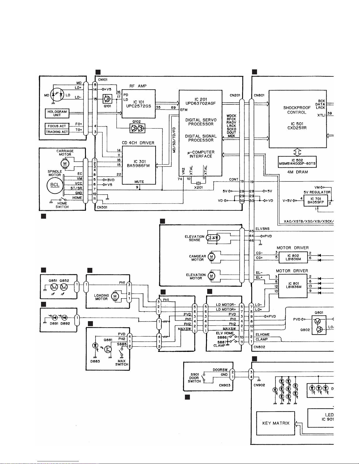
3.1 BLOCK DIAGRAM
MOTOR PCB(A)
F
G
CD CORE UNIT(STS UNIT)
PCB UNIT(B)
H
PCB UNIT(E)
I
PCB UNIT(C)
J
LOAD MOTOR PCB
K
PCB UNIT(D)
M
PCB UNIT(A)
L
Page 11

11
CDX-PD6
A
EXTENDED UNIT
Page 12

12
CDX-PD6
1
23
4
1234
D
C
B
A
A
A-a
BGC
SWITCH PCB
CD CORE UNIT(STS UNIT)
KEYBOARD PCB
3.2 OVERALL CONNECTION DIAGRAM(GUIDE PAGE)
Note: When ordering service parts, be sure to refer to “EXPLODED VIEWS AND PARTS LIST” or “ELECTRICAL PARTS
LIST”.
A-a A-b
A-aA-a
A-b A-b
A-b A-b
A-a A-a
Large size
SCH diagram
Guide page
Detailed page
B
C
Page 13

13
CDX-PD6
5
6
78
5
6
78
D
C
B
A
A-b
A
CEK1018
ILL
GND
BACK UP
KEYBOARD UNIT
Consists of
KEYBOARD PCB
SWITCH PCB
(1/2W)
A
EXTENDED UNIT
Page 14

14
CDX-PD6
1
23
4
1234
D
C
B
A
A-a
A-a
A-b
G
CD CORE UNIT(STS UNIT)
Page 15

15
CDX-PD6
5
6
78
5
6
78
D
C
B
A
A-a
A-a
A-b
B
KEYBOARD PCB
C
SWITCH PCB
BC
Page 16

16
CDX-PD6
1
23
4
1234
D
C
B
A
A-b
A-a
A-b
A
EXTENDED UNIT
Page 17

17
CDX-PD6
5
6
78
5
6
78
D
C
B
A
CEK1018
ILL
GND
BACK UP
KEYBOARD UNIT
Consists of
KEYBOARD PCB
SWITCH PCB
(1/2W)
A-b
A-a
A-b
Page 18

18
CDX-PD6
1
23
4
1234
D
C
B
A
(SERVICE)
M5 SPINDLE
CXM1120
DISC INSERT DETECT
M4 CARRIAGE
CXB3178
2.5V
RF AMP/
AUTO POWER
CONTROL
CD DRIVER
D
E
MOTOR PCB(B)
CD CORE UNIT(SERVO UNIT)
3.3 CD CORE UNIT(SERVO UNIT)
D
E
Page 19

19
CDX-PD6
5
6
78
5
6
78
D
C
B
A
16.934MHz
22/6R3
FOCUS/TRACKING
CARRIAGE/SPINDLE
DIGITAL SERVO
DIGITAL SIGNAL PROCESSOR
D/A CONVERTER
F
D
Page 20

20
CDX-PD6
1
23
4
1234
D
C
B
A
M1 : CXB3174
Q1 : RPI-221
M3 : CXB3175
SURE TRACK
MEMORY CONTRO
+5V REGULATOR
7.5V
9.0V
MOTOR DRIVER
G
F
D
H
LOAD SWITCH
DOOR SWITCH
MODE SWITCH
CD CORE UNIT(STS UNIT)
CD CORE UNIT
(SERVO UNIT)
MOTOR PCB
(A)
ELV SENSE
3.4 CD CORE UNIT(STS UNIT)
F
G
Page 21

21
CDX-PD6
5
6
78
5
6
78
D
C
B
A
22/6R3
RY CONTROLLER
MOTOR DRIVER
4M DRAM
D/A CONVERTER
A
CN101
G
Page 22

22
CDX-PD6
1 RFO 0.5V/div. 0.2µs/div.
Normal mode: play
1 CH1: RFO 1V/div.
2 CH2: MIRR 5V/div.
Test mode: Tracking open
0.5ms/div.
1 CH1: RFO 1V/div.
2 CH2: MIRR 5V/div.
Normal mode: The defect part
passes 500µs/div.
0.5ms/div.
3 CH1: FIN 0.5V/div.
4 CH2: FOP 2V/div.
Test mode: No disc, Focus close
0.2s/div.
3 CH1: FIN 0.5V/div.
5 CH2: FOK 2V/div.
Normal mode: Focus close
0.2s/div.
6 CH1: FEY 0.5V/div.
7 CH2: XSI 2V/div.
Normal mode: Focus close
1ms/div.
8 CH1: TEY 0.5V/div.
9 CH2: TIN 0.5V/div.
Test mode: 32 tracks jump (FWD)
0.5ms/div.
8 CH1: TEY 0.5V/div.
9 CH2: TIN 0.5V/div.
Test mode: Single jump (FWD)
0.5ms/div.
6 CH1: FEY 0.1V/div.
3 CH2: FIN 0.2V/div.
Normal mode: Play
20ms/div.
3 CH1: FIN 0.5V/div.
0 CH2: SIN 1V/div.
Normal mode: Focus close
0.5s/div.
GND
→
GND
→
GND
→
GND
→
- Waveforms
0 SIN 0.5V/div. 0.1s/div.
Normal mode: Play
REFOUT
→
REFOUT
→
REFOUT
→
REFOUT
→
REFOUT
→
REFOUT
→
REFOUT
→
REFOUT
→
REFOUT
→
REFOUT
→
REFOUT
→
REFOUT
→
REFOUT
→
REFOUT
→
REFOUT
→
REFOUT
→
1 RFO 0.5V/div. 0.5µs/div.
Test mode
REFOUT
→
REFOUT
→
REFOUT
→
Note:1. The encircled numbers denote measuring pointes in the circuit diagram.
2. Reference voltage
REFOUT:2.5V
Page 23

23
CDX-PD6
3 CH1: FIN 1V/div.
$ CH2: HOLD 5V/div.
Normal mode:
The defect part passes 800µm
8 CH1: TEY 0.5V/div.
6 CH2: FEY 0.1V/div.
Normal mode: AGC after focus close
8 CH1: TEY 0.5V/div.
! CH2: SD 0.5V/div.
5ms/div.
0 SIN 1V/div. 10ms/div.
Long Search
8 CH1: TEY 1V/div.
# CH2: TEC 1V/div.
Test mode: Focus close
Tracking open
2ms/div.
6 CH1: FEY 0.2V/div.
3 CH2: FIN 0.5V/div.
Normal mode: During
AGC
1ms/div.
@ EFM 1V/div. 2µs/div.
Play
0.2s/div.
% Dout 2V/div. 5µs/div.
Play
^ LRCK 2V/div. 10µs/div. * ADRMON 1V/div. 1s/div.
Normal mode: Starting play
GND
→
REFOUT
→
REFOUT
→
REFOUT
→
REFOUT
→
REFOUT
→
REFOUT
→
REFOUT
→
REFOUT
→
REFOUT
→
REFOUT
→
REFOUT
→
REFOUT
→
REFOUT
→
REFOUT
→
1 CH1: RFO 1V/div.
$ CH2: HOLD 5V/div.
Normal mode:
The defect part passes 800µm
500µs/div.
REFOUT
→
REFOUT
→
8 CH1: TEY 0.2V/div.
9 CH2: TIN 0.5V/div.
Normal mode: During
AGC
1ms/div.
REFOUT
→
REFOUT
→
GND
→
GND
→
500µs/div.
Page 24

24
CDX-PD6
8 CH1: TEY 0.5V/div.
9 CH2: TIN 0.5V/div.
Test mode: 100 tracks jump(FWD)
8 CH1: TEY 0.5V/div.
9 CH2: TIN 0.5V/div.
Normal mode: Play
10ms/div.
5ms/div.
REFOUT
→
REFOUT
→
& SCKO 2V/div. 500ns/div.
Play
REFOUT
→
) CH1: RCH 2V/div.
( CH2: LCH 2V/div.
Normal mode: PLAY (0dB,1kHz)
200µs/div.
AAGND
→
AAGND
→
REFOUT
→
REFOUT
→
Page 25

25
CDX-PD6
1
2
34
1
2
34
D
C
B
A
H
I
J
L
M
K
CXB3177
G
CN802
SWITCH
PCB UNIT(A)
PCB UNIT(C)
PCB UNIT(E)
PCB UNIT(B)
PCB UNIT(D)
LOAD MOTOR PCB
3.5 PCB UNIT(A,B,C,D,E), LOAD MOTOR PCB
M
J
I
H
K
L
Page 26

26
CDX-PD6
1
23
4
1234
D
C
B
A
NOTE FOR PCB DIAGRAMS
1. The parts mounted on this PCB
include all necessary parts for
several destination.
For further information for
respective destinations, be sure
to check with the schematic diagram.
2. Viewpoint of PCB diagrams
IP-BUS
A
A
EXTENDED UNIT
4. PCB CONNECTION DIAGRAM
4.1 EXTENDED UNIT
Capacitor
Connector
P.C.Board
Chip Part
SIDE A
SIDE B
SIDE A
CORD
Page 27

27
CDX-PD6
1
2
34
1
2
34
D
C
B
A
A
G
CN701
CN901
B
A
12
54
3
EXTENDED UNIT
SIDE B
Page 28

28
CDX-PD6
1
23
4
1234
D
C
B
A
4.2 KEYBOARD PCB
B
KEYBOARD PCB
B
A
CN701
C
CN903
SIDE BSIDE A
KEYBOARD PCB
B
Page 29

29
CDX-PD6
1
2
34
1
2
34
D
C
B
A
C
C
SWITCH PCB
B
CN902
SIDE B
SIDE A
SWITCH PCB
4.3 SWITCH PCB
C
Page 30

30
CDX-PD6
1
23
4
1234
D
C
B
A
4.4 CD CORE UNIT(SERVO UNIT)
CD CORE UNIT(SERVO UNIT)
D
E
F
SIDE A
D
PICKUP UNIT(SERVICE)
Page 31

31
CDX-PD6
1
2
34
1
2
34
D
C
B
A
CD CORE UNIT(SERVO UNIT)
D
SIDE B
D
Page 32

32
CDX-PD6
1
23
4
1234
D
C
B
A
4.5 CD CORE UNIT(STS UNIT)
CD CORE UNIT(STS UNIT)
G
H
F
A
CN101
SIDE A
G
Page 33

33
CDX-PD6
1
2
34
1
2
34
D
C
B
A
CD CORE UNIT(STS UNIT)
G
SIDE B
G
Page 34

34
CDX-PD6
1
23
4
1234
D
C
B
A
4.6 MOTOR PCB(A)
M
M3
ELV
M
M1
CAM GEAR
Q1
ELV SENSE
1
25
D
CN201
MOTOR PCB(A)
F
F
SIDE A
Page 35

35
CDX-PD6
1
2
34
1
2
34
D
C
B
A
1
41
G
CN801
MOTOR PCB(A)
F
F
SIDE B
Page 36

36
CDX-PD6
1
23
4
1234
D
C
B
A
4.7 MOTOR PCB(B)
SPINDLE MOTOR
M5
MOTOR PCB(B)
E
E
Page 37

37
CDX-PD6
5
6
78
5
6
78
D
C
B
A
M
M4
CARRIAGE
1
12
D
CN301
E
Page 38

38
CDX-PD6
1
23
4
1234
D
C
B
A
S887
CLAMP
1
11
17
S886
ELV
G
CN802
I
4.8 PCB UNIT(B)
PCB UNIT(B)
H
4.8 PCB UNIT(D)
PCB UNIT(D)
M
H
M
Page 39

39
CDX-PD6
1
2
34
1
2
34
D
C
B
A
1
4
D883
S885
MAX DETECT
Q881
4.10 PCB UNIT(C)
PCB UNIT(C)
J
J
I
Page 40

40
CDX-PD6
1
23
4
1234
D
C
B
A
M
M2
LOADING
1
1
4
2
I
M
4.11 LOAD MOTOR PCB
4.12 PCB UNIT(A)
D891
D892
1
2
LOAD MOTOR PCB
K
PCB UNIT(A)
L
K
L
I
I
E
Page 41

41
CDX-PD6
1
2
34
1
2
34
D
C
B
A
4.13 PCB UNIT(E)
PCB UNIT(E)
I
PCB UNIT(E)
I
I
SIDE A SIDE B
Page 42

42
CDX-PD6
Unit Number : CWM6526
Unit Name : Extended Unit
MISCELLANEOUS
IC 101 IC NJM4558MD
IC 501 IC CA0008AM
IC 601 IC PD5465A
IC 701 IC M62007FP
Q 101 Transistor DTC343TK
Q 102 Transistor DTC343TK
Q 103 Transistor 2SA1586
Q 701 Transistor 2SC2712
Q 702 Transistor 2SC2712
Q 703 Transistor 2SD1760F5
Q 704 Transistor 2SD1007
Q 705 Transistor 2SD1760F5
Q 706 Transistor 2SA1163
Q 707 Transistor 2SC2713
Q 708 Transistor 2SB1335A
Q 709 Transistor DTA124EU
Q 710 Transistor DTC124EU
Q 711 Transistor FMW1
D 101 Diode MA142WA
D 601 Diode MA142WK
D 701 Diode ERC05-10B
D 702 Diode 1SR154-400
D 703 Diode UDZS7R5(B)
D 704 Diode 1SS355
D 705 Diode UDZS5R6(B)
D 706 Diode UDZS9R1(B)
D 707 Diode UDZS6R2(B)
L 701 Coil CTH1190
TH 601 Thermistor CCX1032
X 601 Resonator 6.290MHz CSS1451
RESISTORS
R 101 RS1/16S472J
R 102 RS1/16S472J
R 103 RS1/16S682J
R 104 RS1/16S682J
R 105 RS1/16S622J
R 106 RS1/16S622J
R 107 RS1/16S102J
R 108 RS1/16S102J
R 109 RS1/16S432J
R 110 RS1/16S432J
R 111 RS1/16S103J
R 501 RS1/8S101J
R 502 RS1/8S101J
R 601 RS1/16S473J
R 602 RS1/16S473J
R 603 RS1/16S473J
R 604 RS1/16S102J
R 605 RS1/16S222J
R 606 RS1/16S222J
R 607 RS1/16S222J
R 608 RS1/16S222J
R 609 RS1/16S222J
R 610 RS1/16S222J
R 611 RS1/16S561J
R 612 RS1/16S561J
R 613 RS1/16S561J
R 614 RS1/16S561J
R 615 RS1/16S102J
R 616 RS1/16S473J
R 617 RS1/16S183J
R 618 RS1/16S222J
R 619 RS1/16S0R0J
R 620 RS1/16S473J
R 621 RS1/16S433J
R 622 RS1/16S103J
R 640 RS1/16S471J
R 641 RS1/16S471J
R 642 RS1/16S471J
R 643 RS1/16S471J
R 644 RS1/16S471J
R 649 RS1/16S222J
R 651 RS1/16S222J
R 652 RS1/16S471J
R 653 RS1/16S471J
R 654 RS1/16S471J
R 655 RS1/16S471J
R 656 RS1/16S471J
R 657 RS1/16S471J
R 658 RS1/16S471J
R 659 RS1/16S471J
R 660 RS1/16S471J
R 661 RS1/16S102J
R 662 RS1/16S102J
R 663 RS1/16S102J
R 664 RS1/16S102J
R 665 RS1/16S102J
R 666 RS1/16S471J
R 667 RS1/16S471J
R 668 RS1/16S331J
R 669 RS1/16S331J
R 670 RS1/16S331J
R 671 RS1/16S331J
R 672 RS1/16S331J
R 673 RS1/16S471J
R 674 RS1/16S471J
R 675 RS1/16S471J
R 676 RS1/16S471J
R 677 RS1/16S222J
R 678 RS1/16S222J
R 679 RS1/16S222J
5. ELECTRICAL PARTS LIST
NOTE:
- Parts whose parts numbers are omitted are subject to being not supplied.
- The part numbers shown below indicate chip components.
Chip Resistor
RS1/_S___J,RS1/__S___J
Chip Capacitor (except for CQS.....)
CKS....., CCS....., CSZS.....
=====Circuit Symbol & No.===Part Name Part No.
--- ------ ------------------------------------------ -------------------------
=====Circuit Symbol & No.===Part Name Part No.
--- ------ ------------------------------------------ -------------------------
A
Page 43

43
CDX-PD6
R 680 RS1/16S154J
R 681 RS1/16S222J
R 682 RS1/16S102J
R 683 RS1/16S912J
R 684 RS1/16S473J
R 689 RS1/16S104J
R 690 RS1/16S104J
R 691 RS1/16S273J
R 692 RS1/16S512J
R 693 RS1/16S104J
R 694 RS1/16S104J
R 695 RS1/16S104J
R 696 RS1/16S104J
R 697 RS1/16S222J
R 698 RS1/16S222J
R 699 RS1/16S222J
R 701 RS1/16S104J
R 702 RS1/16S473J
R 703 RS1/8S433J
R 704 RS1/16S273J
R 705 RS1/16S473J
R 706 RS1/16S473J
R 707 RS1/4S103J
R 709 RS1/4S2R2J
R 710 RS1/4S2R2J
R 711 RS1/10S682J
R 716 RS1/16S104J
R 720 RS1/10S102J
R 721 RS1/16S223J
R 722 RS1/16S103J
R 723 RS1/16S223J
R 724 RS1/16S223J
R 730 RS1/10S223J
R 731 RS1/16S101J
R 732 RS1/4S221J
R 733 RS1/16S511J
R 734 RS1/16S681J
R 735 RS1/16S561J
R 736 RS1/16S103J
R 737 RS1/16S273J
R 738 RS1/16S473J
R 739 RS1/16S101J
CAPACITORS
C 101 CEV100M25
C 102 CEV100M25
C 103 CKSRYB222K50
C 104 CKSRYB222K50
C 105 CCSRCH331J50
C 106 CCSRCH331J50
C 107 CEV4R7M35
C 108 CEV4R7M35
C 109 CKSRYB473K16
C 501 CKSQYB102K50
C 502 CKSQYB102K50
C 503 CKSRYB103K50
C 601 CKSRYB104K16
C 603 CKSRYB103K50
C 605 CKSRYB103K50
C 651 CKSRYB103K50
C 701 CEAT471M16
C 703 CEAT471M16
C 704 CKSQYB224K16
C 705 CEV220M6R3
C 706 CKSRYB103K50
C 707 CKSRYB473K16
C 708 CEV4R7M25
C 709 CKSRYB473K16
C 710 CKSRYB473K16
C 711 CKSRYB103K50
C 712 CEV220M16
C 713 CKSRYB473K16
C 714 CEV220M6R3
C 715 CKSRYB473K16
C 720 CKSQYB334K16
C 721 CKSRYB222K50
Keyboard Unit
Consists of
Keyboard PCB
Switch PCB
Unit Number : CWM6131
Unit Name : Keyboard Unit
MISCELLANEOUS
IC 901 IC BU2092FV
D 901 Diode 1SS355
D 902 Diode 1SS355
D 903 Diode 1SS355
D 905 LED CL200PGCTU
D 906 LED CL150DCD(AB)
D 907 LED CL200PGCTU
D 908 LED CL150DCD(AB)
D 909 LED CL200PGCTU
D 910 LED CL150DCD(AB)
D 911 LED CL200PGCTU
D 912 LED CL150DCD(AB)
D 913 LED CL200PGCTU
D 914 LED CL150DCD(AB)
D 915 LED CL200PGCTU
D 916 LED CL150DCD(AB)
D 920 LED CL220PGC
D 921 LED CL220PGC
D 922 LED CL150PGCD(AB)
D 923 LED CL150PGCD(AB)
D 924 LED CL150PGCD(AB)
D 925 LED CL150PGCD(AB)
D 926 LED CL150PGCD(AB)
D 927 LED CL150PGCD(AB)
D 928 LED CL150PGCD(AB)
S 901 Switch CSG1043
S 902 Switch CSG1043
S 903 Switch CSG1043
S 904 Switch CSG1043
S 905 Switch CSG1043
S 906 Switch CSG1043
S 907 Switch CSG1043
S 910 Switch CSN1033
RESISTORS
R 901 RS1/10S561J
R 902 RS1/10S561J
R 903 RS1/10S561J
R 904 RS1/10S561J
R 910 RS1/8S471J
R 911 RS1/8S471J
R 912 RS1/8S471J
R 913 RS1/8S471J
R 914 RS1/8S471J
R 915 RS1/8S471J
=====Circuit Symbol & No.===Part Name Part No.
--- ------ ------------------------------------------ -------------------------
=====Circuit Symbol & No.===Part Name Part No.
--- ------ ------------------------------------------ -------------------------
B C
Page 44

44
CDX-PD6
R 916 RS1/8S471J
R 917 RS1/8S471J
R 918 RS1/8S471J
R 919 RS1/8S471J
R 920 RS1/8S471J
R 921 RS1/8S471J
R 930 RS1/10S331J
R 932 RS1/10S181J
R 933 RS1/10S181J
R 934 RS1/8S471J
CAPACITORS
C 901 CKSQYB104K16
Unit Number : CWX2202
Unit Name : CD Core Unit(Servo Unit)
MISCELLANEOUS
IC 101 IC UPC2572GS
IC 201 IC UPD63702AGF
IC 301 IC BA5986FM
Q 101 Transistor 2SD1664
Q 102 Transistor UMD2N
D 301 Diode 1SR154-400
X 201 Ceramic Resonator 16.934MHz CSS1457
EF 201 Filter CCG1076
RESISTORS
R 101 RS1/8S100J
R 102 RS1/8S120J
R 104 RS1/16S822J
R 105 RS1/16S682J
R 106 RS1/16S183J
R 107 RS1/16S822J
R 108 RS1/16S333J
R 109 RS1/16S683J
R 110 RS1/16S134J
R 111 RS1/16S273J
R 112 RS1/16S222J
R 113 RS1/16S103J
R 114 RS1/16S103J
R 115 RS1/16S102J
R 116 RS1/16S163J
R 117 RS1/16S163J
R 120 RS1/16S101J
R 121 RS1/16S101J
R 125 RS1/16S0R0J
R 201 RS1/16S104J
R 202 RS1/16S473J
R 203 RS1/16S332J
R 204 RS1/16S752J
R 205 RS1/16S752J
R 206 RS1/16S101J
R 250 RS1/16S331J
R 251 RS1/16S331J
R 252 RS1/16S331J
R 253 RS1/16S331J
R 254 RS1/16S331J
R 255 RS1/16S471J
R 256 RS1/16S471J
R 259 RS1/16S221J
R 263 RS1/16S471J
R 269 RS1/16S0R0J
R 274 RS1/16S471J
R 277 RS1/16S471J
R 301 RS1/16S103J
R 302 RS1/16S153J
R 303 RS1/16S103J
R 304 RS1/16S273J
R 305 RS1/16S103J
R 306 RS1/16S752J
R 307 RS1/16S103J
R 308 RS1/16S103J
R 309 RS1/16S471J
R 311 RS1/16S471J
CAPACITORS
C 101 CEV101M6R3
C 102 CKSQYB104K16
C 103 CEV470M6R3
C 104 CKSQYB334K16
C 105 CCSRCH240J50
C 106 CKSRYB222K50
C 107 CEV4R7M35
C 108 CKSRYB273K25
C 109 CCSRCH101J50
C 110 CKSQYB104K16
C 111 CKSRYB332K50
C 112 CKSQYB473K16
C 113 CKSRYB103K25
C 114 CKSRYB391K50
C 115 CCSRCH121J50
C 116 CKSRYB682K50
C 117 CKSRYB333K16
C 118 CKSQYB334K16
C 119 CKSQYB334K16
C 120 CKSQYB334K16
C 121 CKSQYB334K16
C 122 CKSQYB104K16
C 123 CKSRYB472K50
C 124 CKSQYB104K16
C 125 CCSRCH5R0C50
C 126 CKSRYB153K25
C 127 CKSRYB102K50
C 201 CKSQYB334K16
C 202 CKSQYB104K16
C 203 CKSQYB104K16
C 204 CKSRYB471K50
C 207 CKSQYB683K16
C 208 CKSRYB821K50
C 209 CKSRYB273K25
C 210 CKSQYB334K16
C 211 CKSQYB334K16
C 212 CKSQYB334K16
C 213 22µF/6.3V CCH1300
C 301 CEV101M10
C 302 CEV101M10
Unit Number : CWX2203
Unit Name : CD Core Unit(STS Unit)
MISCELLANEOUS
IC 501 IC CXD2511R
IC 502 IC MSM514400DP60TS
IC 601 IC AK4321VF
IC 701 IC BA05SFP
IC 801 IC LB1836M
IC 802 IC LB1836M
Q 801 Transistor DTA123JK
Q 802 Transistor UN2211
D 701 Diode 1SR154-400
D 702 Diode 1SR154-400
=====Circuit Symbol & No.===Part Name Part No.
--- ------ ------------------------------------------ -------------------------
=====Circuit Symbol & No.===Part Name Part No.
--- ------ ------------------------------------------ -------------------------
D
G
Page 45

45
CDX-PD6
D 703 Diode 1SS355
D 704 Diode 1SS355
D 705 Diode 1SS355
D 706 Diode 1SS355
D 707 Diode 1SS355
D 708 Diode 1SS355
S 801 Switch(LOAD) CSN1052
S 802 Switch(DOOR) CSN1052
S 803 Switch(MODE) CSN1052
EF 701 Filter CCG1051
EF 702 Filter CCG1051
RESISTORS
R 501 RS1/16S102J
R 502 RS1/16S202J
R 503 RS1/16S392J
R 504 RS1/16S822J
R 505 RS1/16S163J
R 506 RS1/16S512J
R 507 RS1/16S182J
R 508 RS1/16S222J
R 509 RS1/16S102J
R 510 RS1/16S102J
R 511 RS1/16S102J
R 512 RS1/16S102J
R 513 RS1/16S102J
R 514 RS1/16S471J
R 601 RS1/16S101J
R 602 RS1/16S101J
R 603 RS1/16S471J
R 604 RS1/16S471J
R 701 RS1/10S0R0J
R 702 RS1/10S100J
R 716 RS1/16S471J
R 717 RS1/16S471J
R 718 RS1/16S471J
R 801 RS1/10S102J
CAPACITORS
C 501 CKSQYB334K16
C 502 CKSQYB334K16
C 503 CKSQYB334K16
C 504 CCSRCH471J50
C 506 CCSRCH221J50
C 601 CKSQYB334K16
C 602 CCSRCH221J50
C 603 CKSQYB334K16
C 604 CKSQYB334K16
C 605 22µF/6.3V CCH1300
C 606 CKSQYB334K16
C 701 22µF/6.3V CCH1300
C 702 CEVL101M6R3
C 703 CKSQYB334K16
C 704 CKSQYB334K16
C 801 CKSQYB104K25
C 802 CKSQYB104K25
C 803 CEVL220M16
Unit Number :
Unit Name : PCB Unit(D)
Q 851 Photo-transistor CPT231SXTD
Q 852 Photo-transistor CPT231SXTD
Unit Number :
Unit Name : PCB Unit(E)
R 856 RS1/8S911J
R 857 RS1/8S821J
Unit Number :
Unit Name : PCB Unit(C)
Q 881 Photo-transistor CPT231SXTD
D 883 Chip LED CL202IRXTU
S 885 Switch(MAX) CSN1052
Unit Number :
Unit Name : PCB Unit(A)
D 891 Chip LED CL202IRXTU
D 892 Chip LED CL202IRXTU
Unit Number :
Unit Name : PCB Unit(B)
S 886 Switch(ELV Home) CSN1052
S 887 Switch(Clamp) CSN1051
Unit Number :
Unit Name : Motor PCB(A)
Q 1 Photo-interrupter RPI-221
M 1 Motor Unit(Cam Gear) CXB3174
M 3 Motor Unit(ELV) CXB3175
Unit Number :
Unit Name : Motor PCB(B)
M 4 Motor Unit(Carriage) CXB3178
M 5 Motor(Spindle) CXM1120
Unit Number :
Unit Name : Load Motor PCB
M 2 Motor Unit(Load) CXB3177
Miscellaneous Parts List
Pickup Unit(Service)(P8) CXX1311
=====Circuit Symbol & No.===Part Name Part No.
--- ------ ------------------------------------------ -------------------------
=====Circuit Symbol & No.===Part Name Part No.
--- ------ ------------------------------------------ -------------------------
M
I
J
H
F
E
K
L
Page 46

46
CDX-PD6
• Note :
The grating angle of the PU unit cannot be adjusted after the PU unit is changed. The PU unit in the CD mecha-
nism module is adjusted on the production line to match the CD mechanism module and is thus the best adjusted
PU unit for the CD mechanism module. Changing the PU unit is thus best considered as a last resort. However, if
the PU unit must be changed, the grating should be checked using the procedure below.
• Purpose :
To check that the grating is within an acceptable range when the PU unit is changed.
• Symptoms of Mal-adjustment :
If the grating is off by a large amount symptoms such as being unable to close tracking, being unable to perform
track search operations, or taking a long time for track searching.
• Method :
• Measuring Equipment • Oscilloscope, Two L.P.F.
• Measuring Points • E, F, REFOUT
• Disc • ABEX TCD-784
• Mode • TEST MODE
• Checking Procedure
1. In test mode, load the disc and switch the 5V regulator on.
2. Using the TRK+ and TRK- buttons, move the PU unit to the innermost track.
3. Press key F9 to close focus, the display should read "91". Press key F8 to implement the tracking balance adjustment the display should now read "81". Press key F9 4 times. The display will change, returning to "81" on the
fourth press.
4. As shown in the diagram above, monitor the LPF outputs using the oscilloscope and check that the phase difference is within 75° . Refer to the photographs supplied to determine the phase angle.
5. If the phase difference is determined to be greater than 75° try changing the PU unit to see if there is any
improvement. If, after trying this a number of times, the grating angle does not become less than 75° then the
mechanism should be judged to be at fault.
• Note
Because of eccentricity in the disc and a slight misalignment of the clamping center the grating waveform may be
seen to "wobble" ( the phase difference changes as the disc rotates). The angle specified above indicates the average angle.
• Hint
Reloading the disc changes the clamp position and may decrease the "wobble".
100kΩ
390pF
100kΩ
390pF
E
REFOUT
F
Xch Ych
Oscilloscope
L.P.F.
L.P.F.
E
F
REFOUT
REFOUT
CD CORE UNIT(SERVO UNIT)
6. ADJUSTMENT
CHECKING THE GRATING AFTER CHANGING THE PICKUP UNIT
Page 47

47
CDX-PD6
Grating waveform
Ech → Xch 20mV/div, AC
Fch → Ych 20mV/div, AC
45°
0°
75°
60°
30°
90°
Page 48

48
CDX-PD6
7. GENERAL INFORMATION
7.1 DIAGNOSIS
7.1.1 TEST MODE
- CD Test Mode
1) Precautions on Adjustment
• The unit employs a single voltage (+5V) for the regulator, thus the reference potential of the signal is
RFOUT (approximately 2.5V) rather than GND.
Inadvertent contact of REFOUT and GND during
adjustment can result not only in disabling normal
potential measurement but also in exposing the pickup to strong impacts due to malfunctioning of the
servo. Therefore, you are requested to observe the
following precautions.
• Make sure that the negative probe of the measuring
instrument is not connected to RFOUT or GND.
Special care must be exercised so that the channel 1
negative probe may not be connected to the oscilloscope and the channel 2 negative probe to GND.
Since the frame of the measuring instrument is usually at the same potential as the negative probe, the
frame of the measuring instrument must be changed
to floating status.
When RFOUT is inadvertently connected to GND, you
must immediately turn off the regulator or power
supply.
• The regulator must be turned off before mounting or
dismounting filters or wiring materials.
• You should not start adjustment or measurement
immediately after the regulator is turned on. It is recommended to run the player for approximately one
minute so that it may stabilize.
• When the test mode is turned on, various protective
functions from the software become unavailable.
Thus, you must make sure that undesirable electric or
mechanical shocks are not be given to the system.
• This model employs a photot-ransistor for detecting
discs at their loading or ejection. Thus, if its outer
case is removed during repair work and internal parts
are exposed to light of strong intensity, malfunctions
including the following can result:
∗ The eject button becomes inoperable during play.
Pressing the eject button does not eject a disc and
play is continued.
∗ Loading becomes unavailable.
If a malfunction is recognized, appropriate remedial
actions must be taken. Such actions include changing the light source position, changing the unit position and applying a cover to the photo-transistor.
• When you press the EJECT key to eject a disc, you
must not touch any other key until the ejection is
complete.
• If you press the TRK+ or TRK– for the focus search in
the test mode, you must turn the power off immediately. (Otherwise, the lens will be forced to stick to
the top or bottom, potentially resulting in the burning
of the actuator.)
2) Description of the Test Mode
Adjustment of this unit is done in parallel with the CD
control unit (KEH-P7000 or a head unit conforming to
the IP-BUS specifications), thus key operations for
adjustments are done from the unit. Taking the
example of the KEH-P7000, the following describes
how to turn on the test mode and operate the keys.
The keys referred to in the following are those used
on the KEH-P7000.
• Turning on the Test Mode
Press the [4] and [6] keys simultaneously to turn on
the ACC and the backup.
• Ending the Test Mode
Apply the reset (the reset will be applied two minutes
after the power is turned from off).
• Operation of TR JUMPs (except 100TR) continues
after your finger has left the key. CRG, MOVE and
100TR JUMP are forced to the tracking close mode as
soon as the key is released.
• Turning the power on or off resets the JUMP MODE
to the Single TR.
Page 49

49
CDX-PD6
[BAND]
Power Off
TRK
MIN
SEC
[F.9]
Focus Close/S-curve/
F, F0 Measurement
TRK
MIN
SEC
91
91 91
[F.12]
Focus Mode Select
TRK
MIN
SEC
0X
0X 0X
[F.7]
Tracking Servo
Close
TRK
MIN
SEC
00
00 00
[BAND]
Power ON
(T.OFFSET adjustment required)
TRK
MIN
SEC
00
00 00
[F.9]
Power ON
(T.OFFSET adjustment not required)
TRK
MIN
SEC
99
99 99
[F.7]
Mechanism Test Mode
Initial State
TRK
MIN
SEC
72
0* **
[F.12]
New Test Mode
[CD]or[SOURCE]
Source CD
TRK
MIN
SEC
[BAND]
Power Off
TRK
MIN
SEC
[F.7]
Tracking Close
(AGC, Applicable Servo)
TRK
MIN
SEC
XX
XX XX
[F.12]
Tracking Close
(No AGC, Applicable Servo)
TRK
MIN
SEC
XX
XX XX
[F.9]
Auto Adjustment Display
/Rough Servo
TRK
MIN
SEC
??
?? ??
[F.8]
Tracking Balance
Adjustment
TRK
MIN
SEC
8X
8X 8X
[Key]
Contents
Display
[4]+[6]+Reset
Test Mode In
[F.9]
AGC
TRK
MIN
SEC
XX
XX XX
[F.12]
CRG/TR Jump Count
Select
TRK
MIN
SEC
XX
XX XX
[TRK+]
CRG+/TR Jump+
TRK
MIN
SEC
XX
XX XX
[TRK-]
CRG–/TR Jump–
TRK
MIN
SEC
XX XX
[F.10]
SPINDLE
Uniform/
Double Switching
TRK
MIN
SEC
XX
XX XX
[BAND]
Power Off
TRK
MIN
SEC
[F.7]
AGC/F.BIAS
Display Switching
TRK
MIN
SEC
??
?? ??
TRK
MIN
SEC
99
99 99
or
[TRK+]
CRG+
TRK
MIN
SEC
00
00 00
TRK
MIN
SEC
99
99 99
or
[TRK-]
CRG-
TRK
MIN
SEC
00
00 00
TRK
MIN
SEC
99
99 99
or
[TRK+]
CRG+
TRK
MIN
SEC
8X
8X 8X
TRK
MIN
SEC
9X
9X 9X
or
[TRK-]
CRG-
TRK
MIN
SEC
8X
8X 8X
TRK
MIN
SEC
9X
9X 9X
or
[BAND]
Power Off
TRK
MIN
SEC
[F.8]
Trackig Open
TRK
MIN
SEC
8X
8X 8X
TRK
MIN
SEC
9X
9X 9X
or
[F.8]
Trackig Open
TRK
MIN
SEC
8X
8X 8X
TRK
MIN
SEC
9X
9X 9X
or
*1
*6
*5
*3
*2
*2
*4
The following operation instructions are based on an older type operation head unit.
For an operation of the new type head unit, refer to the conversion table (Note).
Note: The older operation head unit: Provided with 1 to 12 DISC selects.
The new operation head unit: Provided with 1 to 6 DISC selects.
*1) Switching must take place in the following sequence.
TRK
MIN
SEC
00
00
00
TRK()
MIN
SEC
99
99
99
S.Curve Check
TRK
MIN
SEC
01
01
01
Focus EQ Measurement.Focus Close
TRK
MIN
SEC
02
02 02
*2)
→→ → → →
9X(8X):91(81)
4 TR
92(82)
10 TR
93(83)
32 TR
94(84)
100 TR
95(85)
CRG Move
96(86)
Switching must take place in the following sequence.
*4)
→→→
F.AGC Gain F.AGC Gain F. BIAS Setting
(AGC Gain = (Current value/Initial value) x 20)
→→→
→→
Single TR /4TR / 10TR / 32TR / 100TR
Single TR
*3) Switching must take place in the following sequence.
It applies to the CRB Move and 100TR Jump alone.
Min/Sec (or Track No.)
*5) Switching must take place in the following sequence.
F.Cancel Display
*6) Switching must take place in the following sequence.
T.Offset Display T.Bal Display
Rough Servo.
(F.Bias value, F.Cancel value, T.Offset value, T.Bal value
= (Upper 8 bits of the setting (7F[H] to 80[H] + 128)/4
= 63[D] to 32[D] to 00[D]).
•
•
•
Operation of TR JUMPs other than 100TR is continued after your finger has left the key.
CRG Move and 100TR Jump are forced to the Tracking Close Mode when the key is released.
Powering on or off resets the Jump Mode to the Single TR (9).
When ending the test mode, apply the reset (the reset is applied in two minutes from powering off).
Note:
Note:
Note:
The IP-BUS head unit must be employed for controlling the test mode.
Sound is unavailable even after the tracking has been closed
(this trouble results when the IC for the STS is not controlled in the test mode).
When you pressed the [TRK+] or [TRK-] key during the Focus Search, you must turn the power off immediately
(otherwise, the lens can stick resulting in actuator damages).
[Key]
Older unit
[BAND]
15 00H
[TRK+]
15 01H
[TRK-]
15 02H
[F.7]
15 03H
[F.8]
15 04H
[F.9]
15 05H
[F.10]
15 06H
[F.11]
15 07H
[F.12]
15 08H
[Key]
New unit
[BAND]
15 00H
[TRK+]
15 01H
[TRK-]
15 02H
[1]
15 03H
[2]
15 04H
[3]
15 05H
[4]
15 06H
[5]
15 07H
[6]
15 08H
Operation
Test Mode
New Test Mode
Power ON/OFF
CRG+/TR Jump+
(Toward outer perimeter)
Tracking Close/AGC gain,
F.Bias adjustment value display switching
Auto Tracking Balance adjustment/
Tracking Open
Focus Close, S.Curve, F.EQ measurement/
Rough Servo/AGC
Focus Open
Jump Off
Focus Mode select/Tracking Close/
CRG*TR Jump Switching
CRG-/TR Jump(Toward inner perimeter)
Error occurrence time/
Cause display switching
Track+/FF
Track-/REV
Mode
RAMDOM
Auto/Manual switching
- CD Player Flowchart
Page 50

50
CDX-PD6
[BAND]
Mechanism Test
initialized
TRK
MIN
SEC
[F.7]
CAMMOTOR
select
TRK
MIN
SEC
72
1* **
[F.8]
ELVMOTOR
select
TRK
MIN
SEC
72
2* **
[F.9]
LOADMOTOR
select
TRK
MIN
SEC
72
3* **
[F.7]
Mechanism Test In
Initial State
TRK
MIN
SEC
72
0* **
[BAND]
CD Test Mode
TRK
MIN
SEC
00
00 00
[F.12]
New Test Mode
[CD]or[SOURCE]
Source CD
TRK
MIN
SEC
[Key]
Contents
Display
[4]+[6]+Reset
Test Mode In
[F.10]
CAM+LOADMOTOR
select
TRK
MIN
SEC
72
4* **
[TRK+]
MOTOR FWD drive
TRK
MIN
SEC
72
** **
❏ Operating Procedures:
1)
2)
3)
4)
Turn on the CD Test Mode, then select the
CD-MULTI for the SOURCE.
Press [F.7] to turn on the Mecha Test Mode.
Select the motor to be driven
using the [F.7] to [F.10] keys.
Press the [TRK+] or [TRK–] in this state to drive
the selected motor.
[Key]
Older unit
[BAND]
15 00H
[TRK+]
15 01H
[TRK–]
15 02H
[F.7]
15 03H
[F.8]
15 04H
[F.9]
15 05H
[F.10]
15 06H
[Key]
New unit
[BAND]
15 00H
[TRK+]
15 01H
[TRK–]
15 02H
[1]
15 03H
[2]
15 04H
[3]
15 05H
[4]
15 06H
Operation
Mechanism Test is initialized.
Valid only when the motor selected (using the
[F.7] to [F.10] keys) is driven in FWD direction.
CAMMOTOR is selected.
[F.9]
CD Test Mode
TRK
MIN
SEC
99
99 99
[TRK+]
MOTOR REV drive
TRK
MIN
SEC
72
** **
TRK
MIN
SEC
72
X*
**
()
Valid only when the motor selected (using the
[F.7] to [F.10] keys) is driven in REV direction.
ELVMOTOR is selected.
LOADMOTOR is selected.
CAM + LOADMOTOR is selected.
<Screen Display during Mecha Test Mode>
TRK 72 MIN ** SEC
##
TRK : 72
72 : Mecha Test Mode
is turned on
MIN : Upper (10th order):
Type of motors selected
Lower (order of 1): State of DISC
sensing phototransistor and switch
1* : CAM motor
2* : ELV motor
3* : LOAD motor
4* : CAM+LOAD motor
PH1 PH2
MAXSW
Display
L
H
L
H
L
H
L
H
L
L
H
H
L
L
H
H
L
L
L
L
H
H
H
H
*0
*1
*2
*3
*4
*5
*6
*7
L:H:Phototransistor is OPEN and switch is ON.
Phototransistor is CLOSE and switch is OFF.
SEC : 1 When ELV motor is selected, ELV position is displayed
01: ELV at home position (1st disc).
10: ELV at a position other than home (2nd to 6th). * Note 1.
11: ELV moving to a specified position.
00: Reserved (for an error)
2 When CAM.LOAD motor is selected:
Indicates CAMSW (CAM gear) status.
EJECT
SW1 (DOORSW)
SW2 (LOADSW)
SW3 (MODESW)
SW4 (CLAMPSW)
Display
10
30
31
21 20
222333 32
REV
FWD
Note 2
An example when TRK 72, MIN 10 and SEC 31:
Test Mode is turned on from TRK 72.
CAMMOTOR is selected from 1 of MIN 10 and PH1/PH2
are selected from 0. All MAX switches are set to L (low).
As for SEC 31, since CAMMOTOR is selected from MIN,
CAM gear CLAMP switch is set to L (low) and others are
H (high) from SEC1.
❏ Precautions
*
*
Note 1:
Note 2:
The keys are inoperable as long as operation of the mechanism is continued.
When driving the CAMMOTOR in 31 → 30 → 10 (in REV direction),
the elevation position must be at the EJECT/LOAD position (the top position).
When the elevation is situated at the Note 1 position, move of any motor
other than the REV is disabled.
Before performing the elevation, make sure that the CAM SW (switch) is
set to a position between 22 and 20.
As a rule, driving of the ELV MOTOR must be started immediately after
the CAMSW indication has changed from 22 to 20.
clamp
- CD Changer Mechanism Flowchart
Page 51

51
CDX-PD6
❍ Operating Procedures for Ejecting a Clamped Disc
[F.7]
Selects CAMMOTOR
Press [TRK–]. Display changes sequentially through 32→33→23→22.
Want to eject the currently clamped disc?
Using the [F.7], drive the elevation until the display changes from 22 to 20.
[F.8]
Selects ELVMOTOR.
Using the [TRK–], drive the elevation down until 0.1 is displayed.
Using the [TRK+], drive the elevation up until the 10 is displayed (the
disc position).
[F.7]
Selects CAMMOTOR.
Using the [TRK+], drive the CAMMOTOR until the 10 is displayed changes from 20 (or 22) to 21 and 31.
[F.8]
Selects ELVMOTOR.
Using the [TRK+], drive the tray of the disc to be ejected up to the top position (Display 10).
[F.10]
Selects CAM+LOADMOTOR.
Using the [TRK+], drive the CAM+LOADMOTOR until the display changes from 32 to 30 and 10.
As the elevation is driven into the vicinity of a position where 10 is indicated for the status display,
the door will open and part of the disc will be pushed out.
[F.9]
Selects LOADMOTOR.
Press the [TRK+] to eject the disc.
01→11→10→11→10→11→10→11→10→11→10
1st disk
2nd disk
3rd disk
4th disk
5th disk
6th disk
1
2
2
3
4
5
6
YES
NO
1
2
3
4
5
6
Select CAMMOTOR using [F.7], then press the [TRK–] while the disc is being clamped (CAMSW state is 32).
The CAMSW status indication sequentially changes through 32→33→23→22.
When the disc to be ejected is not identical with the disc being clamped, select the [F.8] ELVMOTOR in the vicinity of where
the display changes from 22 to 20, then match the elevation to the disc to be ejected according to the following procedures:
After selecting ELVMOTOR, lower the elevation until the ELV position display becomes 01 (1st disc) using the [TRK-].
Drive the elevation up until the display is changed to 10. This is the elevation where the second disk is situated.
The next display of 10 tells you the elevation of the 3rd disc. Repeating this operation allows you to establish an elevation
matching each disc. (When the elevation is driven from the 1st through 6th disc, the status display changes as
01→11→10→11→10→11→10→11→10→11→10.)
(When the disc to be ejected coincides with the disc being clamped, the above operations are not necessary.)
Select the [F.7] CAMMOTOR and then, using the [TRK+], drive it until the display changes from 20 (or 22) to 21 and 31.
Select the [F.8] ELVMOTOR, then drive the tray of the disc to be ejected up to the EJECT/LOAD position (using the [TRK+]).
Select the [F.10] CAM+LOADMOTOR, then drive it in the REV direction until the display changes from 31 to 30 and 10.
The door will open immediately before the display changes to 10 and part of the disc will be pushed out.
When 10 is displayed, select the [F.9] LOADMOTOR, then drive it in REV direction until the disc is completely ejected.
Page 52

52
CDX-PD6
- New Test Mode
Principally, discs are played normally in this test mode.
When the test mode has been turned on, it will indicate when (in absolute time) and why an error occurred. Errors
include off-focus, spindle lock disengagement, unavailability of sub-code reading and sound skipping.
While the test mode setup is taking place, operational status (Internal RAM: CPOINT) of the CD control software is
displayed.
(1) Turning On the New Test Mode
Refer to the Test Mode Flowchart on page 49.
(2) Cause-of-Error (Error No.) Codes
Error code Category Troubles Description/Cause(s)
40 Electric system Off-focus FOK = LOW has continued for 100 msec. or more.
→ Due to scratches, stains, vibrations, servo failure, etc.
41 Electric system Spindle lock LOCK = LOW has continued for 100 msec. or more.
disengagement → Due to scratches, stains, vibrations, servo failure, etc.
42 Electric system Unavailability of Sub-code was unreadable for 500 msec.
sub-code reading → Due to scratches, stains, vibrations, servo failure, etc.
43 Electric system Sound skipping Last address memory has been activated.
→ Due to scratches, stains, vibrations, servo failure, etc.
* The error codes are displayed in the same manner as in the normal mode.
(3) Display of Operational Status During Setup
Status No. Contents Protective Action
01 Carriage returning to home position None
02 Carriage moving to inner perimeter 10-second time-out, failure on home switch.
03 Carriage moving to outer perimeter 10-second time-out, failure on home switch.
05 Carriage outer perimeter feed (1 second) taking place None
11 Setup started None
12 Spindle rotation None
Focus search started
13 Waiting for focus close (XSL = L) Focus close not available
10 Waiting for focus close (FOK = H) Improper focus close
(When AGC has not been conducted)
14 Waiting for focus close (FOK = H) Improper focus close
(When AGC has already been conducted)
15,16,17 Focus CLOSE Off-focus
Tracking OPEN
18 Focus AGC in progress Off-focus
19 Tracking AGC in progress Off-focus
20 Waiting for MIRR, LOCK and sub-code. Off-focus, failure on MIRROR, spindle lock
Carriage close, servo applicable to CLV. unavailable, sub-code unreadable.
* "Setup" denotes a series of operations from establishing the focus up to playing a disc.
Page 53

53
CDX-PD6
(5) LCD Display Example
• While the setup is in progress
8-digit indication LCD
• The operation mode (PLAY, SEARCH, etc.) is identical
with the normal mode.
• When a protection/error has occurred (8-digit indication LCD)
(a) Error display
Display can be switched
from the BAND key
(b)Display of occurrence No. and occurrence time
(in absolute time)
ERROR–xx
TNo.10Min40Sec
05
- Error No. Display
The error mode is turned on if a CD player becomes not playable or is forced to halt due to an error. Cause(s) of an
error will be indicated with numerical characters. The error-number-display function is intended to facilitate the
error analysis and resulting repair work.
(1) Basic Display Means
• Display examples: E-XX (4-digit), ERR-XX (6-digit) and ERROR-XX (8-digit)
(2) Error Code
Error code Category Troubles Description/Cause(s)
10 Electricity Carriage home error Unable to move to or from inner perimeter
→
Failure on home switch or carriage move trouble.
11 Electricity Focus search error Unable to set a focus
→
Scratches or stains on backside of the disc, severe vibrations,
CD-R is not written to the disc
(it can happen on the backside of the disc).
12 Electricity Spindle lock error Spindle lock unavailable, sub-code unreadable
Sub-code error
→
Failure on spindle, scratches on the disc, stains or strong
vibrations.
14 Electricity Mirror error MIRR signal error continues for 500 msec or more
→
Stains on the disc or strong vibrations.
17 Electricity Setup error AGC protection cannot be turned on in time or focus can be easily lost
→
Scratches or stains on the disc or strong vibrations.
19 Electricity Setup error Tracking error level is low or tracking balance adjustment is unavailable
→
Failure on the pickup or tracking-error circuit.
30 Electricity Search time-out Target address can't be reached
→
Failure on the carriage/tracking or scratches on the disc.
A0 System Error on power supply Ground fault of power supply (VD)
→
Failure on switching transistor or failure of power supply.
TNo.11Min11Sec
11
Page 54

54
CDX-PD6
Code Name Description
20 Door OPENING While the mechanism is in operation, should have been closed a door
was opened.
21 Roller OFF time-out 4 seconds have elapsed before completing the roller OFF
(the cam gear has not been rotated to the roller-OFF end position).
22 Roller SET time-out 4 seconds have elapsed before completing the roller SET.
(Roller OFF time-out) (During the roller OFF operation, 4 seconds have elapsed while the cam
gear is rotating in REV direction.)
23 Door CLOSING Door can't be closed when the roller OFF has ended.
24 Cam started from invalid position The cam gear attempted to do roller OFF/roller SET from an invalid
position.
26 Foreign substance on phototransistor Foreign substance was found on the phototransistor when closing the
(before closing the door) door after the loading is complete.
An error will be indicated if the disc is still caught by the
phototransistor after 4 seconds of forced eject.
29 Roller being caught Although the cam gear has been rotated up to the roller OFF end
position, the roller can't be moved to the standby position.
41 Lift DOWN time-out 4 seconds have elapsed before completing the lift DOWN operation.
42 Lift UP time-out 4 seconds have elapsed before completing the lift UP operation.
(Lift DOWN time-out) (During the lift DOWN operation, 4 seconds have passed with the cam
gear rotating in REV direction.)
45 Lift DOWN cam displacement The lift DOWN complete cam gear has been displaced from its
specified position.
52 EJECT time-out 8 seconds have elapsed before completing the EJECT operation.
An error will be indicated if the disc is still caught by the
phototransistor after 4 seconds of forced eject.
55 HOME SW ON after forced EJECT HOME SW was still at ON position after 4 seconds of forced eject.
57 Phototransistor being caught When forced eject was employed for the Bup failure during loading or
after forced EJECT ejection,an error will be indicated if the disk is still caught by the
phototransistor after 4 seconds of forced eject.
61 CRGIN time-out 10 seconds have elapsed before completing CRGIN operation.
(CRGOUT time-out) (During CRGOUT operation, 10 seconds have elapsed with the cam
gear rotating in REV direction.)
62 CRGOUT time-out 10 seconds have elapsed before completing the CRGOUT operation.
65 CRGOUT cam displacement Position of the CRGOUT complete cam gear has been displaced.
71 ELVUP time-out 2 seconds have elapsed before completing 1-stage UP.
72 ELVDN time-out 2 seconds have elapsed before completing 1-stage DOWN.
74 ELV displacement At the start of ELV, ELVSNS was not set to low.
(In case of starting from the 1st floor, ELHOME was not set to low.)
75 ELV counting error HLHOME was set to low though not on the 1st floor.
(There is a conflict between the floor number stored on the
microcomputer and the actual floor number.)
91 LOAD time-out 8 seconds have elapsed before completing the LOAD.
An error will be indicated if the disc is still caught by the
phototransistor after 4 seconds of forced eject.
96 Settlement of foreign substance Unauthorized foreign substance such as 8 cm disc has been loaded.
An error will be indicated if the disc is still caught by the
phototransistor after 4 seconds of forced eject.
Page 55

55
CDX-PD6
7.1.2 DISASSEMBLY
- Removing the Extend Unit (Fig. 1)
1. Remove the three screws B, then remove the side
frame and holder.
2. Remove screw C, screw D and PCB from the connector.
3. Straighten the three currently bent claws, then
remove the extend unit.
- Removing the CD Mechanism Module (Fig. 2)
1. Remove the three screws A, then remove the
front frame.
2. Remove the three screws B and two screws C,
then remove the damper and holder.
3. Remove the two spring As, spring B and spring
C from the hook, then remove the CD mechanism module.
- Removing the Keyboard PCB (Fig. 3)
1. Remove screws A and B, then remove the switch
PCB.
2. Remove the four screws D, then remove the
guide.
3. Remove the three screws C, then remove the keyboard PCB.
– Precautions on Assembly –
Apply spring C (black) to the front
side hook.
Remaining springs A and B are to be
hung on the center hook.
– Precautions on Assembly (Fig. 4) –
When mounting the switch PCB,
lower the white lever so as to prevent
the switch arm from bending.
Fig. 1
Fig. 2
Fig. 3
Fig. 4
Holder
Holder
Holder
Damper
Front Frame
Damper
Damper
Damper
Holder
Holder
Grille
PCB
- Removing the Grille Assy (Fig. 1)
1. Remove the two screws A and the connector,
then remove the grille assy.
- Removing the upper case (not shown)
1. Remove the five screws, then remove the upper
case.
Extend Unit
Side Frame
CD Mechanism Module
Switch PCB
Guide
Grille Unit
Keyboard PCB
Page 56

56
CDX-PD6
- How to remove the Tray Assy
1. Apply about 6V current to the Cam gear motor until
all holes match at the position (A) (elevation OK position).
2. Hook the three springs B temporarily as shown in Fig.
5. While pushing the Tray holder lock arms (right and
left) in the direction (C), remove the Tray holder.
3. Lift up the Tray assy to remove it.
* Be careful not to remove the Tray hooks from the Tray
assy.
- How to remove the Carriage Mech Assy
1. Insert a short pin into the flexible PCB of the Pickup
unit.
2. While opening the resin hooks, remove the cover
from the Servo unit.
3. Disconnect the flexible PCBs from the connectors
CN101 and CN301.
4. Remove the Tray holder and the Tray assy. (See
above)
5. Rotate the Cam gear motor until the positions of all
holes (E) match, then stop the motor.
(The Carriage Mech assy will stop as shown in the
Fig.7.)
* When the positions of all holes match, they will be
completely covered by the Carriage mech assy.
* To rotate the Cam Gear motor, see "How to remove
the Tray assy".
6. Unhook the spring A.
7. Remove the flexible holder B (while opening the
hooks).
8. Remove the flexible PCB (C) from the motor. (The
flexible PCB (C) has been stuck on the motor with
double-sided adhesive tape.)
9. Loosen the fixing screw and remove the flexible
holder.
ELV motor
Cam gear motor
Approximately DC 6V
Tray holder
Tray holder lock arm
Tray holder
lock arm
Tray
hooks
Tray Assy
Cover
CN101
CN301
Match the hole positions
Flexible
holder
Fig.5
Fig. 6
Fig. 7
Short pin
Tray
hooks
Page 57

57
CDX-PD6
- How to remove the Pickup unit
1. Remove the pulling spring, torsion spring and Eshaped ring. Then remove the Clamper arm.
* The spring (A) will be removed with the Clamper
arm.
10. Remove the screw, pressure spring and collar. Lift
up the Carriage mechanism assy to remove it.
* Screw tightening torque: 2.6kgfcm
2. Slide the Clamp UP lever (B) to remove it.
3. Loosen the 2 screws. Remove the feed-screw cover
by sliding it.
4. Remove the feed-screw pressure spring (D).
5. Loosen the 2 screws. Remove the feed-screw holder
(E).
6. Remove the belt.
7. Remove the Pickup unit together with the feed screw.
* Be careful not to lose the shaft holders at the both
ends of the feed screw.
* Be careful not to damage the 2 flexible PCBs(for the
Pickup and motor) when separating them. The flexible PCBs have been stuck each other with doublesided adhesive tape.
Carriage mechanism Assy
Screw
Collar
Pressure spring
Clamper arm
E-shaped ring
Pulling spring
Torsion spring
White
Black
Pickup
unit
Feed screw
Belt
Carriage
motor
Fig. 8
Fig. 9
Fig. 10
Page 58

58
CDX-PD6
7.2 IC
- Pin Functions (PD5465A)
Pin No. Pin Name I/O Function and Operation
1 VDIN I VD power supply sensor input
2 DOORSW I Door open position sense input
3 IPIN I IP-BUS data input
4 IPOUT O IP-BUS dada output
5 CLMPSW I Disk clamp sense input
6 ELHOME I Elevation sense input
7 XSCK O LSI clock output
8 XSO O LSI data output
9 XSI I LSI data input
10 xstb O LSI strobe output
11 xrst O LSI reset output
12 XA0 O LSI data discernment control signal output
13 VDCONT O VD power supply control output
14 EJKEY I Eject key input
15 asens I ACC power sense input
16 IPPOW O BUS driver power supply control output
17 LOADSW I Loading sense input
18 ELVSW I Elevation OK input
19–21 NC Not used
22 bsens I Back up power sense input
23 SBSY I Signal indicating head of subcode block input
24 NC Not used
25 reset I Reset input
26 POWER O +5V power supply control output
27 CONT O Servo driver power supply control output
28 XIN I Crystal oscillating element connection pin
29 XOUT O Crystal oscillating element connection pin
30 VSS GND
31–33 KST1-3 O Key strobe output
34,35 kd!,kd@ I Key data input
36–38 NC Not used
39 TESTIN I Test program mode input
40 DCLOSE I Door close sense input
41 WDSL O Data comparison designation output
42 XWIH I DRAM data white inhibit input
43 XEMP I DRAM data read inhibit input
44 CHDT I Data comparison mode monitor input
45,46 CHM0,1 O Data comparison mode output
8. Loosen the 2 screws. Remove the plate spring and
the rack.
9. Pull out the feed screw from the Pickup unit.
Rack
Plate spring
Feed screw
Pickup
unit
Grease (White: KD-1)
Grease (Yellow:
PG-641)
Fig. 11
Grease (Yellow:
PG-641)
Page 59

59
CDX-PD6
Pin No. Pin Name I/O Function and Operation
47-49 NC Not used
50 XWRE O DRAM data white enable output L:enable
51 XRDE O DRAM data read enable output L:enable
52 WQOK O SUB-Q OK output L:SUBQ OK
53 EMPH O DAC EMPH output
54 SCONT O Double speed select output
55 LOAD O PHOT power supply control output
56 CDMUTE O Mute output
57,58 LO2,LO1 O Load motor control output
59,60 ELV2,1 O ELV motor control output
61,62 CG2,1 O CAM motor control output
63 MIRR I Mirror detector input
64 LOCK I Spindle lock detector input
65 FOK I FOK signal input
66 EXSCK O Shift clock output
67 EXMODE O Latch clock output
68 EXSO O Serial data output
69 EXCE O Chip enable output
70 ILPOW O Illumination power supply control output
71 VCC Power supply terminal
72 VREF I A/D converter reference voltage input
73 AVSS I A/D converter GND
74 ADRMON I DRAM memory remaining monitor input
75 EREF I DRAM A/D converter reference voltage input
76,77 PH1,2 I Disc photo sense input
78 MAXSW I MAX switch input
79 ELVSNS I ELV position sense input
80 TEMP I Temperature detector input
80
1
20
21 40
41
60
61
*PD5465A
IC's marked by* are MOS type.
Be careful in handling them because they are very
liable to be damaged by electrostatic induction.
Page 60

60
CDX-PD6
20
19
18
17
VDD
oe
Q11
Q10
16
15
14
13
Q9
Q8
Q7
NC
12
11
NC
Q6
1
2
3
4
VSS
DATA
CLOCK
LCK
5
6
7
8
Q1
Q2
Q3
Q4
9
10
Q5
Q0
Output buffer (Open drain)
12bit storage-register
12bit shift-register
Control circuit
BU2092FV
28
27
26
25
PreVcc
OPIN4(+)
OPIN4(-)
OPOUT4
24
23
22
OPIN3(+)
OPIN3(-)
OPOUT3
21
20
19
18
GND
STBY
PowVcc
VO3(-)
17
16
15
VO3(+)
VO4(-)
VO4(+)
1
2
3
4
BIAS IN
OPIN1(+)
OPIN1(-)
OPOUT1
5
6
7
OPIN2(+)
OPIN2(-)
OPOUT2
8
9
10
11
GND
MUTE
PowVcc
VO2(-)
12
13
14
VO2(+)
VO1(-)
VO1(+)
Stand-by
Mute
Level shift
Level shift
Level shift
Level shift
BA5986FM
Page 61

61
CDX-PD6
MSM514400DP-60TS
26
25
24
22
VSS
DQ4
DQ3
oe
23
cas
18
17
16
14
A8
A7
A6
A4
15
A5
1
2
3
5
4
9
10
11
13
12
DQ1
DQ2
we
A9
ras
A0
A1
A2
VCC
A3
Timing
Generator
Column
Address
Buffers
Timing
Generator
Column
Decoders
Write
Clock
Generator
Internal
Address
Counter
Refresh
Control
Clock
Sense
Amplifiers
I/O
Selector
Output
Buffers
Input
Buffers
Row
Address
Buffers
Row
Decoders
Word
Drivers
Memory
Cells
On Chip
Vbb Generater
10
10
10
10
4
4
4
4
4
4
4
8
7
6
5
1
2
3
4
reset
CD
VCC
NC
int
GND
NC
NC
Interrupt signal
generate block
Reset signal
generate block
M62007FP
Page 62

62
CDX-PD6
1
2
3
4
CHDT
AM19
AM18
AM17
5
6
7
8
AM15
TST0
VSS
SPSL
9
10
XRST
AM16
11
12
13
14
TST1
DTSL
CHM0
CHM1
15
16
XWRE
WDSL
17
18
19
20
XRDE
XQOK
XSOE
SDTO
21
22
23
24
SCK
XLT
VDD
DATA
25
26
BCK
SDTI
27
28
29
30
LRCK
WDCK
WDCI
LRCI
31
32
BCKI
DATI
48
47
46
45
XOE
XCAS
D3
D2
44
43
42
41
D0
MCSL
C176
VSS
40
39
XTLI
D1
38
37
36
35
XTLO
OSCE
NC
MCK
34
33
RFCK
XROI
64
63
62
61
XEMP
XWIH
NC
A4
60
59
58
57
A6
A7
A8
VDD
56
55
A3
A5
54
53
52
51
A2
A1
A0
A9
50
49
XWE
XRAS
Timing
controller
CPU
interface
VWA
register
CK
generator
WA
generator
RA
generator
Remain area
calcurator
S/P
P/S
Status
controller
Data
comparator
RAM
interface
Selector
CXD2511R
Page 63

63
CDX-PD6
8. OPERATIONS AND SPECIFICATIONS
8.1 OPERATIONS
65421 3
Key Finder
CD indicators
A CD is loaded.
The unit is in the CD loading standby mode.
Green
Flashing
The unit is standing by during ejection of all the CDs.
Lit
Status
Flashing
Lit
Orange
Out
The currently selected CD.
A CD is being loaded, changed or ejected.
No CD is loaded.
Power is switched OFF.
Disc loading slot
CD indicators
Buttons 1–6
EJECT button
Page 64

CDX-PD6
General
Power source .......... 14.4 V DC (10.8 – 15.1 V allowable)
Grounding system ........................................ Negative type
Max. current consumption ........................................ 1.3 A
Dimensions
(mounting size) ........ 178 (W) × 50 (H) × 165 (D) mm
[7 (W) × 2 (H) × 6-1/2 (D) in.]
(nose) .......................... 170 (W) × 46 (H) × 19 (D) mm
[6-3/4 (W) × 1-3/4 (H) × 3/4 (D) in.]
Weight ...................................................... 1.5 kg (3.3 lbs.)
CD player
System .................................... Compact disc audio system
Usable discs .................................................. Compact disc
Signal format .................... Sampling frequency: 44.1 kHz
Number of quantizatin bits: 16; linear
Frequency characteristics ............ 20 – 20,000 Hz (±1 dB)
Signal-to-noise ratio ...... 92 dB (1 kHz) (IHF-A network)
Distortion .............................................................. 0.006%
Dynamic range ............................................ 92 dB (1 kHz)
Output level ........................................ 1.0 V (1 kHz, 0 dB)
Number of channels ............................................ 2 (stereo)
Note:
• Specifications and the design are subject to possi-
ble modification without notice due to improvements.
Connection Diagram
Fuse resistor
This product
Fuse holder
Toterminal always supplied
with power regardless of
ignition switch position.
Tovehicle (metal) body.
Orange
Black (ground)
Tolighting switch terminal.
Yellow
IP-BUS (Blue)
Head unit
(sold separately)
IP-BUS input
(Blue)
Note:
The electrical leads of this product may be different colors to the corresponding
leads (i.e. the leads that serve the same function) of other products. When
connecting this product to another product, please read the instruction
manual for each product carefully and then connect each lead of this product
to the other product that serves the same function.
8.2 SPECIFICATIONS
 Loading...