

Page 1
PIONEER ELECTRONIC CORPORATION 4-1, Meguro 1-Chome, Meguro-ku, Tokyo 153-8654, Japan
PIONEER ELECTRONICS SERVICE INC. P.O.Box 1760, Long Beach, CA 90801-1760 U.S.A.
PIONEER ELECTRONIC [EUROPE] N.V. Haven 1087 Keetberglaan 1, 9120 Melsele, Belgium
PIONEER ELECTRONICS ASIACENTRE PTE.LTD. 253 Alexandra Road, #04-01, Singapore 159936
C PIONEER ELECTRONIC CORPORATION 1999
K-ZZY. MAY 1999 Printed in Japan
ORDER NO.
CRT2388
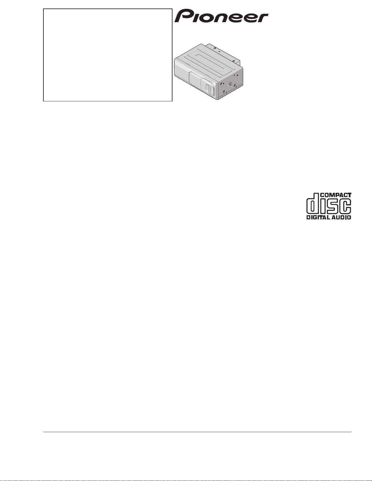
VOICE CONTROL MULTI-CD PLAYER
CDX-P2050VC X1N/UC
CONTENTS
1. SAFETY INFORMATION ............................................3
2. EXPLODED VIEWS AND PARTS LIST.......................4
3. BLOCK DIAGRAM AND SCHEMATIC DIAGRAM...12
4. PCB CONNECTION DIAGRAM ................................26
5. ELECTRICAL PARTS LIST ........................................34
6. ADJUSTMENT..........................................................39
7. GENERAL INFORMATION .......................................45
7.1 DIAGNOSIS ........................................................45
7.1.1 TEST MODE..............................................45
7.1.2 DISASSEMBLY .........................................54
7.2 IC .........................................................................56
8. OPERATIONS AND SPECIFICATIONS.....................65
- See the separate manual CX-938(CRT2357) for the CD mechanism description, disassembly and circuit
description.
- The CD mechanism employed in this model is one of C8 series.
CDX-P2050VC/X1N/UC
CDX-P2050VN X1N/EW
CDX-P2050VS X1N/EW
Page 2
2
CDX-P2050VC,P2050VN,P2050VS
- CD Player Service Precautions
1. For pickup unit(CXX1285) handling, please refer
to"Disassembly"(See page 54). During replacement,
handling precautions shall be taken to prevent an
electrostatic discharge(protection by a short pin).
2. During disassembly, be sure to turn the power off
since an internal IC might be destroyed when a connector is plugged or unplugged.
3. Please checking the grating after changing the pickup
unit(see page 39) since these screws protects the
mechanism during transport, be sure to affix it when
it is transported for repair, etc.
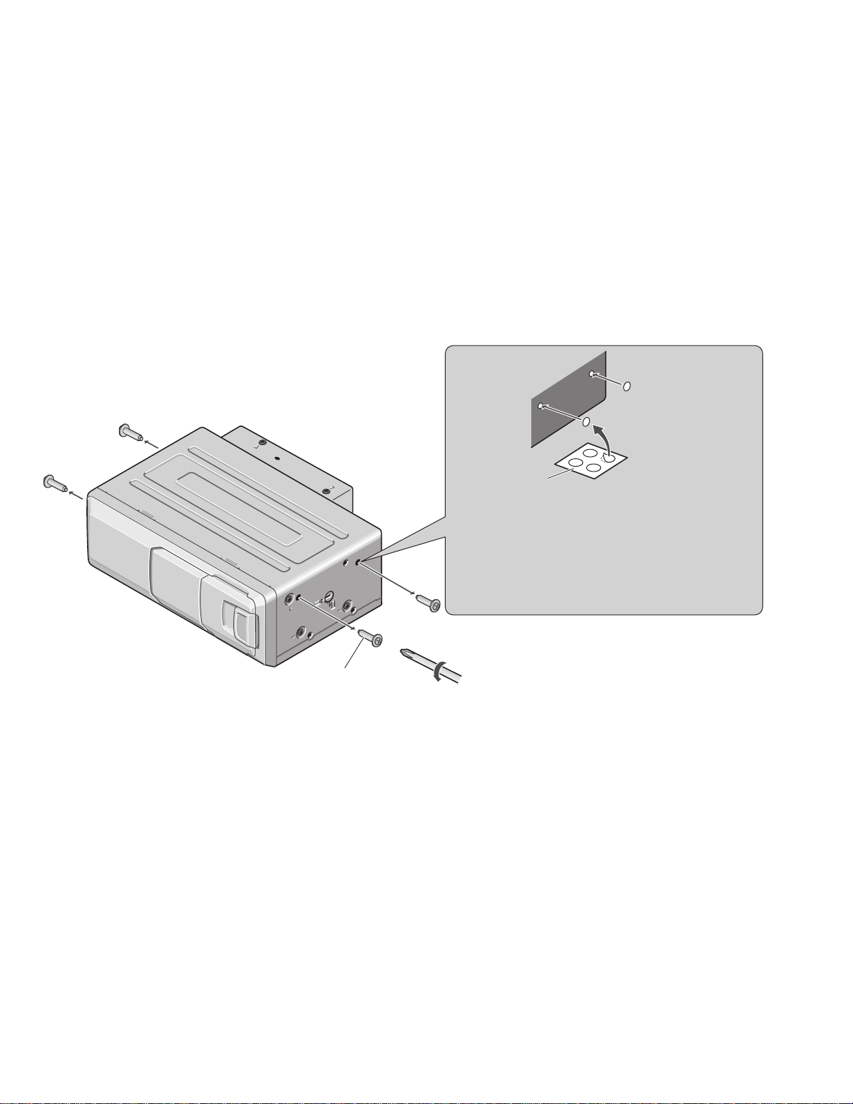
Transport screw
Attach to the original position before transporting the set.
Seal
After removing the transport screw, cover the hole
with the supplied seal.
Transportation of multi-CD Player
A transport screw has been attached to the set in order to protect it
during transportation. After removing the transport screw, cover
the hole with the supplied seal. Be sure to remove the transport
screw before mounting the set. The removed transport screw
should be retained in the accessory bag for use the next time the
set is transported.
Page 3
3
CDX-P2050VC,P2050VN,P2050VS
1. SAFETY INFORMATION
1.1 CDX-P2050VC/X1N/UC
CAUTION
This service manual is intended for qualified service technicians; it is not meant for the casual do-it-yourselfer.
Qualified technicians have the necessary test equipment and tools, and have been trained to properly and safely repair
complex products such as those covered by this manual.
Improperly performed repairs can adversely affect the safety and reliability of the product and may void the warranty.
If you are not qualified to perform the repair of this product properly and safely; you should not risk trying to do so
and refer the repair to a qualified service technician.
W
ARNING
This product contains lead in solder and certain electrical parts contain chemicals which are known to the state of
California to cause cancer, birth defects or other reproductive harm.
Health & Safety Code Section 25249.6 - Proposition 65
1.2 CDX-P2050VN/X1N/EW and CDX-P2050VS/X1N/EW
1. Safety Precautions for those who Service this Unit.
• Follow the adjustment steps (see pages 39 through 44)in the service manual when servicing this unit. When checking or adjusting the emitting power of the laser diode exercise caution in order to get safe, reliable results.
Caution:
1. During repair or tests, minimum distance of 13cm from the focus lens must be kept.
2. During repair or tests, do not view laser beam for 10 seconds or longer.
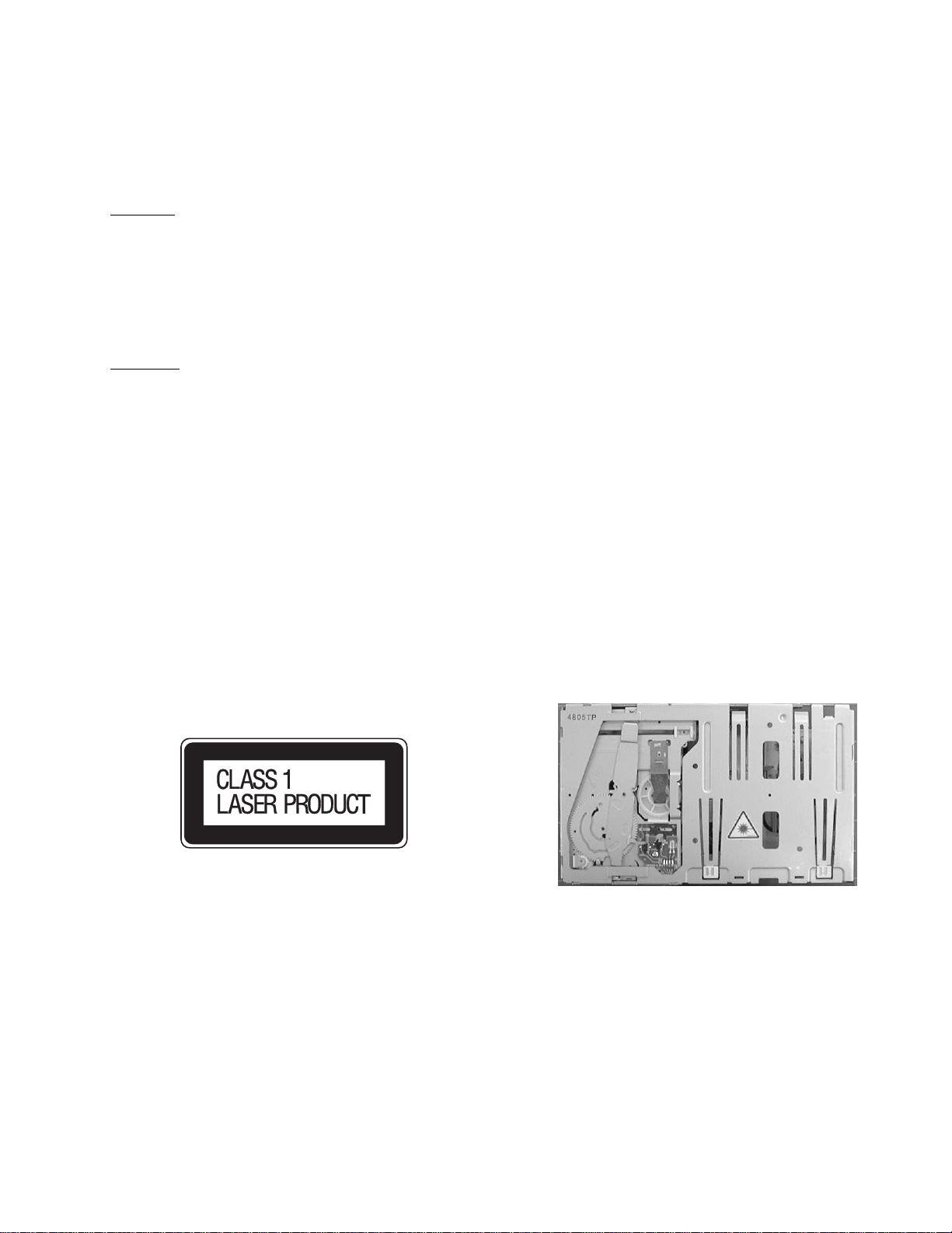
2. A “CLASS 1 LASER PRODUCT” label is affixed to the
rear of the player.
3. The triangular label is attached to the mechanism
unit frame.
4. Specifications of Laser Diode
Specifications of laser radiation fields to which human access is possible during service.
Wavelength = 800 nanometers
Page 4
4
CDX-P2050VC,P2050VN,P2050VS
2. EXPLODED VIEWS AND PARTS LIST
2.1 PACKING
12
11
11
12
8
9
19
10
7
13
14
21
20
5
4
3
1
6
2
16
17
15
18
23
27
26
25
22
28
29
30
24
31
33
32
Page 5
5
CDX-P2050VC,P2050VN,P2050VS
Part No.
Mark No. Description CDX-P2050VC/X1N/UC CDX-P2050VN/X1N/EW CDX-P2050VS/X1N/EW
1 Screw Assy CEA1962 CEA1962 CEA1962
2 Screw CBA1295 CBA1295 CBA1295
* 3 Polyethylene Sheet CNM5158 CNM5158 CNM5158
4 Screw(M6X16) HMB60P500FMC HMB60P500FMC HMB60P500FMC
5 Screw HMF40P080FZK HMF40P080FZK HMF40P080FZK
6 Nut NF60FMC NF60FMC NF60FMC
* 7 Polyethylene Bag CEG1099 CEG1099 CEG1099
8 Polyethylene Bag CEG1185 CEG1026 CEG1026
9 Carton CHG3790 CHG3788 CHG3789
10 Contain Box CHL3790 CHL3788 CHL3789
11 Protector CHP2156 CHP2156 CHP2156
12 Protector CHP2157 CHP2157 CHP2157
13 Seal CNM5599 CNM5741 CNM5741
14-1 Owner’s Manual CRD3003 CRD3005 CRD3007
14-2 Installation Manual CRD3004 CRD3006 CRD3008
* 14-3 Caution Card CRP1205 CRP1205 CRP1205
* 14-4 Warranty Card Not used CRY1087 CRY1087
15 Magazine Assy CXB4028 CXB4028 CXB4028
16 Angle Assy CXB4345 CXB4344 CXB4344
17 Angle CNB2447 CNB2440 CNB2440
18 Controller Assy CXB3633 CXB3633 CXB3633
19 Cord CDE5831 CDE5830 CDE5831
* 20 Caution Card CRP1090 CRP1090 CRP1090
* 21 Caution Card CRP1196 CRP1196 CRP1196
22 Accessory Assy CEA2508 CEA2508 CEA2508
23 Cord CDE6004 CDE6004 CDE6004
24 Cord Clamper Assy CEA2072 CEA2072 CEA2072
25 Cord Clamper CNV2581 CNV2581 CNV2581
* 26 Polyethylene Bag E36-615 E36-615 E36-615
* 27 Polyethylene Bag CEG-238 CEG-238 CEG-238
28 Fastener(rough) CNM3709 CNM3709 CNM3709
29 Fastener(soft) CNM3710 CNM3710 CNM3710
30 Clamper CNV3751 CNV3751 CNV3751
31 Microphone Assy CPM1017 CPM1017 CPM1017
32 Cushion MEH1007 MEH1007 MEH1007
33 Clip Stand MNK1221 MNK1221 MNK1221
- Owner’s Manual
Model Part No. Language
CDX-P2050VC/X1N/UC CRD3003 English, French
CDX-P2050VN/X1N/EW CRD3005 English, French, German, Dutch
CDX-P2050VS/X1N/EW CRD3007 English, Spanish, Italian, Portuguese(B)
- PACKING SECTION PARTS LIST
NOTE:
- Parts marked by “*”are generally unavailable because they are not in our Master Spare Parts List.
- Screws adjacent to
∇ mark on the product are used for disassembly.
- Installation Manual
Model Part No. Language
CDX-P2050VC/X1N/UC CRD3004 English, French
CDX-P2050VN/X1N/EW CRD3006 English, French, German, Dutch
CDX-P2050VS/X1N/EW CRD3008 English, Spanish, Italian, Portuguese(B)
Page 6
6
CDX-P2050VC,P2050VN,P2050VS
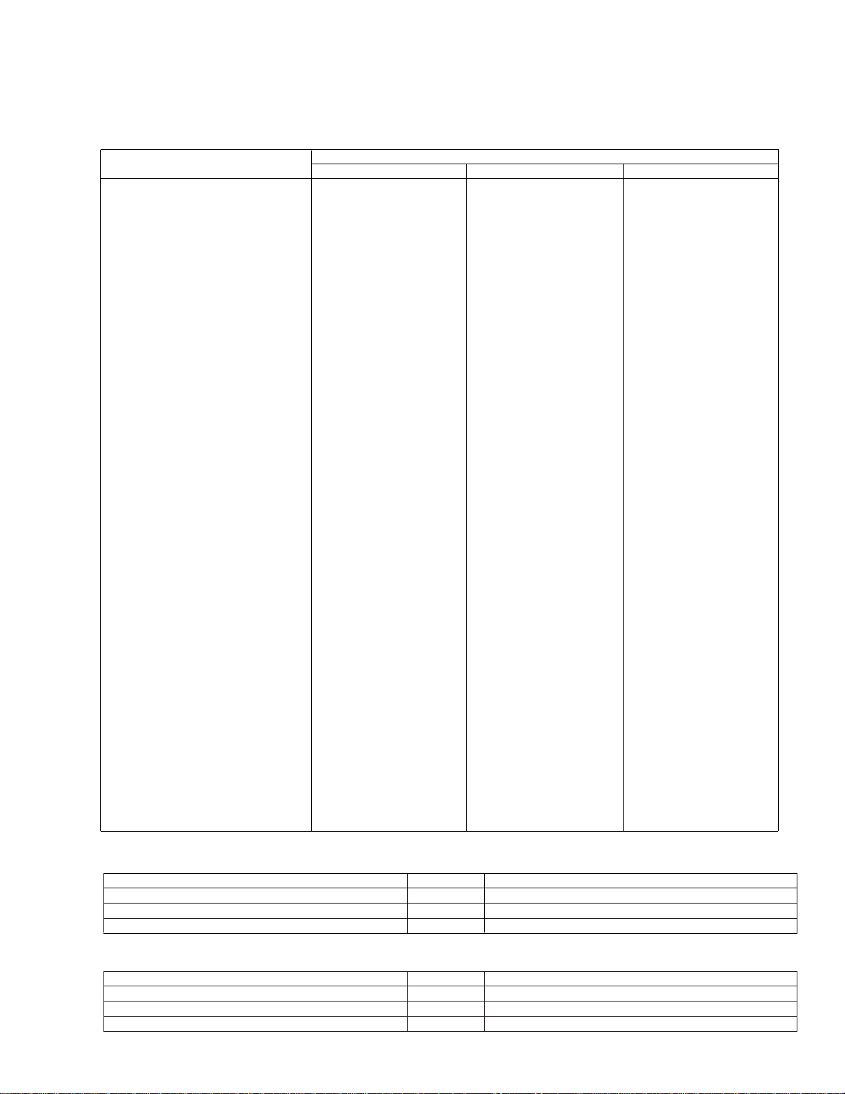
2.2 EXTERIOR
Page 7

7
CDX-P2050VC,P2050VN,P2050VS
1 Screw BMZ26P040FMC
2 Screw BMZ30P040FZK
3 Button(EJECT) CAC6363
4 Screw(M4X4) CBA1353
5 Spring CBH1862
6 Connector CDE5525
7 Connector CDE6002
8 Cord
See Contrast table(2)
9 Controller Assy CXB3633
10 Cord CDE6004
11 Upper Case
See Contrast table(2)
12 Arm CNC8058
13 Insulator CNM6074
14 Panel CNS5218
15 Damper CNV5227
16 Power Unit CWM6365
17 Screw BMZ26P060FMC
18 Plug(CN991) CKS-460
19 Connector(CN921) CKS3407
20 Connector(CN911) CKS2222
21 Holder CNC8059
22 Holder CNC8060
23 Lower Case Unit
See Contrast table(2)
24 Grille Unit See Contrast table(2)
25 Screw BPZ20P080FMC
26 Door
See Contrast table(2)
27 Door See Contrast table(2)
28 Holder CNC8141
29 Lever
See Contrast table(2)
30 Connector(CN922) CKS3599
31 •••••
32 •••••
33 CD Mechanism Module CXK4920
34 Screw IMS20P035FZK
35 Screw IMS26P040FMC
36 Transistor(Q910) 2SD2396
37 Cord Assy CDE5992
38 Case
See Contrast table(2)
39 Screw BSZ30P040FZK
40 Voice Unit
See Contrast table(2)
41 Connector(CN901) CKS3763
42 Connector(CN303) CKS3585
43 Screw BMZ26P060FMC
44 IC(IC71) NJM7805FA
45 Holder CNC8209
46 Holder CNC8422
47 Clamper CEF1008
48 Sheet CNM6531
49 Cord Assy MDE1099
50
Vibration Prevention Material MED1008
51 Connector(CN1) MKP1029
52 Button A MNK1294
53 Button B MNK1295
54 Case MNK1298
55 PCB Assy MWM1073
56 Grille Assy MXX1105
57 Screw PPZ26P080FZK
58 Cushion TED1366
(1) EXTERIOR SECTION PARTS LIST
Mark No. Description Part No. Mark No. Description Part No.
Part No.
Mark No. Symbol and Description CDX-P2050VC/X1N/UC CDX-P2050VN/X1N/EW CDX-P2050VS/X1N/EW
8 Cord CDE5831 CDE5830 CDE5831
11 Upper Case CNB2446 CNB2445 CNB2445
23 Lower Case Unit CXB3398 CXB3397 CXB3397
24 Grille Unit CXB4394 CXB4396 CXB4395
26 Door CAT2023 CAT2008 CAT2008
27 Door CAT2024 CAT2009 CAT2009
29 Lever CNS5393 CNS5357 CNS5357
38 Case CNB2493 CNB2441 CNB2441
40 Voice Unit CWM6367 CWM6367 CWM6366
(2) CONTRAST TABLE
CDX-P2050VC/X1N/UC, CDX-P2050VN/X1N/EW and CDX-P2050VS/X1N/EW are constructed the same
except for the following:
Page 8
8
CDX-P2050VC,P2050VN,P2050VS
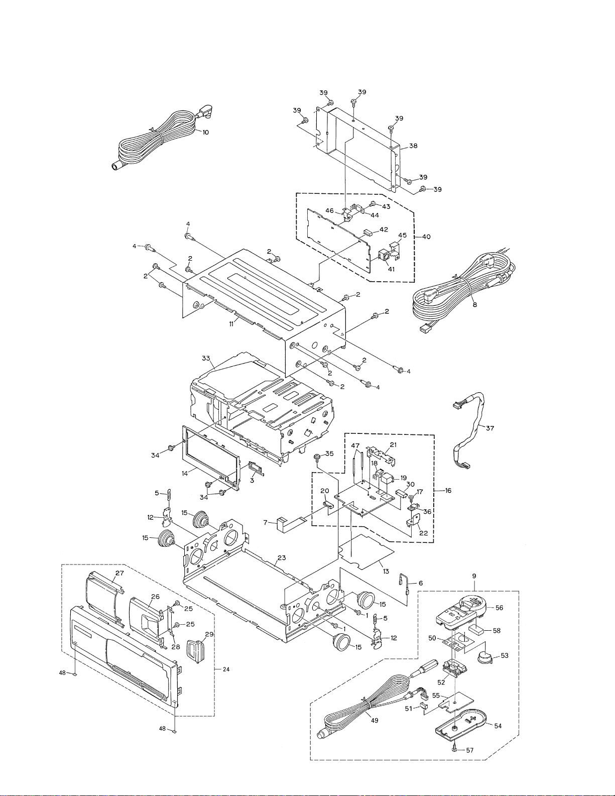
2.3 CD MECHANISM MODULE
Page 9

9
CDX-P2050VC,P2050VN,P2050VS
1 Connector CDE6069
2 CD Core Unit(C8) CWX2277
3 Connector(CN701) CKS1953
4 Connector(CN101) CKS2272
5 Screw BMZ20P025FMC
6 Screw CBA1037
7 Screw CBA1041
8 Screw CBA1176
9 Screw CBA1362
10 Screw CBA1387
11 Screw CBA1493
12 Screw CBA1476
13 Screw CBA1486
14 Washer CBF1038
15 Spring CBH1867
16 Spring CBH2172
17 Spring CBH2173
18 Spring CBH2174
19 Spring CBH2175
20 Spring CBH2177
21 Spring CBH2178
22 Spring CBH2179
23 Spring CBL1390
24 Spring CBL1392
25 Spring CBL1404
26 Short Pin CBL1239
27 Volume(VR801) CCW1024
28 Screw CBA1491
29 Shaft CLA3304
30 Arm CNC7901
31 Lever CNC7905
32 Lever CNC7906
33 Arm CNC7908
34 Arm CNC7909
35 Holder CNC7911
36 Holder CNC7912
37 Lever CNC7919
38 Stopper CNC7920
39 Frame CNC7921
40 Lever CNC7922
41 Bracket CNC7923
42 Lever CNC7924
43 Frame CNC7927
44 Frame CNC7928
45 Bracket CNC8355
46 Plate CNC8375
47 Cover CNC8434
48 Sheet CNM6009
49 Spacer CNM6146
50 Sheet CNM6296
51 PCB CNP5227
52 PCB CNP5228
53 Ball CNR1189
54 Gear CNR1531
55 Belt CNT1086
56 Gear CNV5472
57 Gear CNV5473
58 Rail CNV5920
59 Lever CNV5475
60 Gear CNV5477
61 Arm CNV5478
62 Holder CNV5480
63 Guide CNV5921
64 Guide CNV5922
65 Holder CNV5483
66 Holder CNV5484
67 Clamper CNV5485
68 Gear CNV5486
69 Gear CNV5562
70 Holder CNV5563
71 Stopper CNV5564
72 Lighting Conductor CNV5785
73 Mechanism PCB CWX2303
74 Connector(CN801) CKS1965
75 Connector(CN802) CKS3486
76 Damper Unit CXA7159
77 Chassis Unit CXB2850
78 •••••
79 Chassis Unit CXB2851
80 Arm Unit CXB2855
81 Screw Unit CXB2857
82 •••••
83 Frame Unit CXB4427
84 Magazine Holder Unit CXB4460
85
Motor Unit(M851)(SPINDLE) CXB3003
86
Motor Unit(M854)(CARRIAGE) CXB3004
87 Screw JFZ20P025FMC
88 Motor Unit(M853)(TRAY) CXB4421
89 Screw JFZ20P025FMC
90 Motor Unit(M852)(ELV) CXB3006
Mark No. Description Part No. Mark No. Description Part No.
- CD MECHANISM MODULE SECTION PARTS LIST
Page 10

10
CDX-P2050VC,P2050VN,P2050VS
91 Screw JFZ20P025FMC
92 Lever Unit CXB3938
93 •••••
94 Gear Unit CXB4338
95 Screw JGZ17P025FZK
96 Pickup Unit(Service) CXX1285
97 •••••
98 •••••
99 Screw IMS26P040FMC
100 Screw JFZ20P025FNI
101 Photo-transistor(Q851) PT4800
102
Spring Switch(S851,S853) CSN1051
103 LED(D851) CN504-2
104 Spring Switch(S852) CSN1052
Mark No. Description Part No.
Page 11
11
CDX-P2050VC,P2050VN,P2050VS
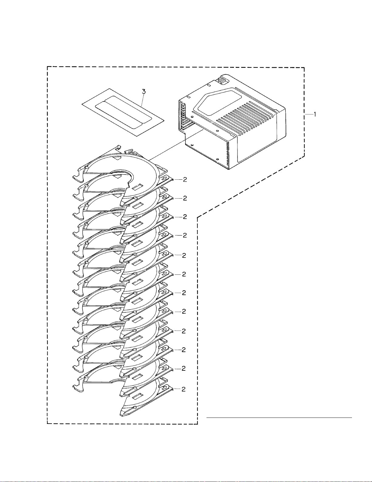
2.4 MAGAZINE ASSY
1 Magazine Assy CXB4028
2 Tray CNV5341
3 Label CRW1396
- MAGAZINE ASSY SECTION PARTS LIST
Mark No. Description Part No.
Page 12
12
CDX-P2050VC,P2050VN,P2050VS
1
23
4
1234
D
C
B
A
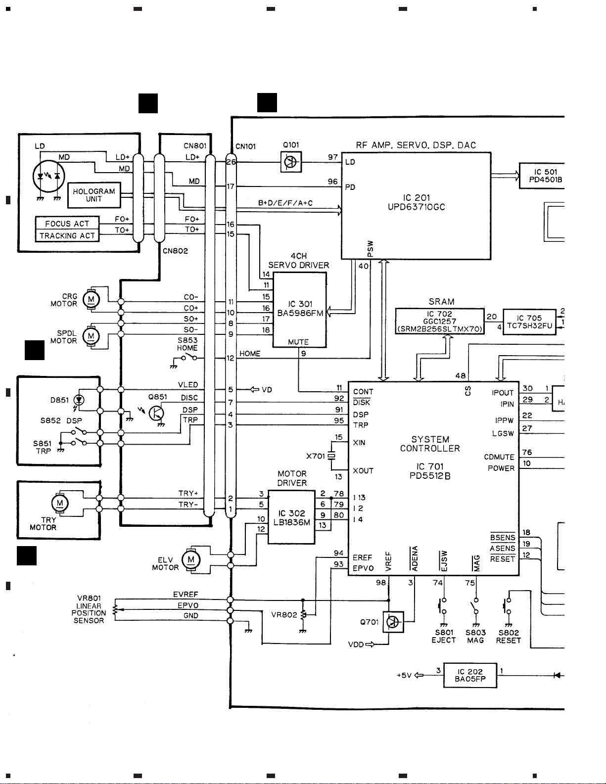
3. BLOCK DIAGRAM AND SCHEMATIC DIAGRAM
3.1 BLOCK DIAGRAM
A
CD CORE UNIT
C
MECHANISM
PCB
PICKUP UNIT (SERVICE)
D
SWITCH PCB
E
MOTOR PCB
Page 13
13
CDX-P2050VC,P2050VN,P2050VS
5
6
78
5
6
78
D
C
B
A
B
POWER UNIT
F
CN303
Page 14

14
CDX-P2050VC,P2050VN,P2050VS
1
23
4
1234
D
C
B
A
F
VOICE UNIT
G
PCB ASSY
Page 15
15
CDX-P2050VC,P2050VN,P2050VS
5
6
78
5
6
78
D
C
B
A
B
CN922
Page 16
16
CDX-P2050VC,P2050VN,P2050VS
1
23
4
1234
D
C
B
A
3.2 OVERALL CONNECTION DIAGRAM
Note: When ordering service parts, be sure to refer to “EXPLODED VIEWS AND PARTS LIST” or “ELECTRICAL
PARTS LIST”.
M854
CXB3004
M851
CXB3003
M852
CXB3006
M853
CXB4421
1
12
6
8
13
21
9
11
10
4
CN801
CN802
C
MECHANISM
PCB
D
SWITCH PCB
E
MOTOR PCB
PICKUP UNIT(SERVICE) CXX1285
MOTOR DRIVER
4CH SERVO DRIVER
RF-AMP,SERVO,DSP
CN101
10K
C
D
E
A
1/2
Page 17
17
CDX-P2050VC,P2050VN,P2050VS
5
6
78
5
6
78
D
C
B
A
18
7
2
5
19
20
15
17
16
3
9
11
A
CD CORE UNIT
RIVER
A
2/2
A
1/2
Page 18
18
CDX-P2050VC,P2050VN,P2050VS
1
23
4
1234
D
C
B
A
A
2/2
A
1/2
SYSTEM CONTROLLER
PD5512B
Page 19
19
CDX-P2050VC,P2050VN,P2050VS
5
6
78
5
6
78
D
C
B
A
A
2/2
R769(1/8W)
R768(1/8W)
B
POWER UNIT
IP-BUS DRIVER
SRAM
CN701
CN911
Page 20
20
CDX-P2050VC,P2050VN,P2050VS
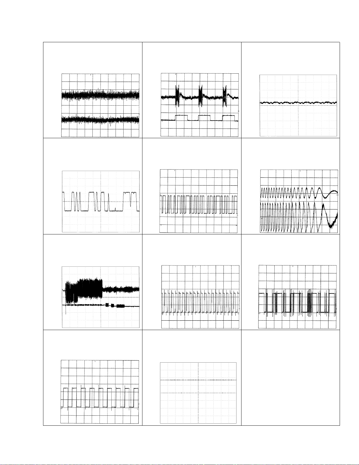
1 RFI 0.5V/div. 0.5µs/div.
Normal mode: play
1 CH1: RFI 1V/div.
2 CH2: MIRR 5V/div.
Test mode: Tracking open
0.5ms/div.
1 CH1: RFI 1V/div.
2 CH2: MIRR 5V/div.
Normal mode: The defect part
passes 800µm
0.5ms/div.
3 CH1: FD 0.5V/div.
4 CH2: FOR 2V/div.
Test mode: No disc, Focus close
0.2s/div.
3 CH1: FD 0.5V/div.
5 CH2: FOK 2V/div.
Normal mode: Focus close
0.2s/div.
6 CH1: FE 0.5V/div.
7 CH2: XSI 2V/div.
Normal mode: Focus close
1ms/div.
REFO
→
8 CH1: TE 0.5V/div.
9 CH2: TD 0.5V/div.
Test mode: 32 tracks jump (REV)
0.5ms/div.
8 CH1: TE 0.5V/div.
9 CH2: TD 0.5V/div.
Test mode: Single jump (REV)
0.5ms/div.
8 CH1: TE 0.5V/div.
9 CH2: TD 0.5V/div.
Test mode: 100 tracks jump (REV)
5ms/div.
6 CH1: FE 0.1V/div.
3 CH2: FD 0.2V/div.
Normal mode: Play
20ms/div.
3 CH1: FD 0.5V/div.
0 CH2: MD 1V/div.
Normal mode: Focus close (12cm)
0.5s/div.
3 CH1: FD 0.5V/div.
0 CH2: MD 1V/div.
Normal mode: Focus close (8cm)
0.5s/div.
REFO
→
REFO
→
REFO
→
REFO
→
REFO
→
REFO
→
GND
→
REFO
→
REFO
→
REFO
→
REFO
→
REFO
→
REFO
→
REFO
→
REFO
→
REFO
→
REFO
→
REFO
→
REFO
→
- Waveforms
Note:1. The encircled numbers denote measuring pointes in the circuit diagram.
2. Reference voltage
REFO:2.5V
REFO
→
REFO
→
REFO
→
REFO
→
Page 21
21
CDX-P2050VC,P2050VN,P2050VS
8 CH1: TE 0.2V/div.
9 CH2: TD 0.2V/div.
Normal mode: play
8 CH1: TE 0.5V/div.
! CH2: SD 0.5V/div.
TEST mode:100Tracks jump(FWD)
5ms/div.
0 MD 0.5V/div. 0.1s/div.
Normal mode: Play (12cm)
0 MD 1V/div. 10ms/div.
Long Search (12cm)
@ EFM 1V/div. 5µs/div.
Normal mode: Play
8 CH1: TE 1V/div.
# CH2: TEC 1V/div.
Test mode: Focus close
Tracking open
2ms/div.
8 CH1: TE 0.5V/div.
6 CH2: FE 0.5V/div.
Normal mode:
AGC after focus close
0.2s/div.
20ms/div.
% SCKO 2V/div. 1µs/div.
Normal mode: Play
^ DOUT 2V/div. 10µs/div.
Normal mode: Play
& LRCK 2V/div. 20µs/div.
Normal mode: Play
* VD 5V/div. 50ms/div.
Normal mode: No disc
GND
→
REFO
→
REFO
→
GND
→
REFO
→
REFO
→
REFO
→
REFO
→
REFO
→
REFO
→
REFO
→
REFO
→
REFO
→
GND
→
REFO
→
GND
→
REFO
→
GND
→
REFO
→
Page 22

22
CDX-P2050VC,P2050VN,P2050VS
( CH1: R OUT 2V/div.
) CH2: L OUT 2V/div.
Normal mode: Play (1kHz 0dB)
6 CH1: FE 0.2V/div.
3 CH2: FD 0.5V/div.
Normal mode: During AGC
1ms/div.
8 CH1: TE 0.2V/div.
9 CH2: TD 0.5V/div.
Normal mode: During AGC
1 CH1: RFI 1V/div.
⁄ CH2: HOLD 5V/div.
Normal mode: The defect part passes
800µm(B.D)
500µs/div.
1ms/div.
0.5ms/div.
3 CH1: FD 1V/div.
⁄ CH2: HOLD 5V/div.
Normal mode: The defect part passes
800µm(B.D)
0.5ms/div.
9 CH1: TD 0.1V/div.
⁄ CH2: HOLD 5V/div.
Normal mode: The defect part passes
800µm(B.D)
0.5ms/div.
REFO
→
REFO
→
REFO
→
REFO
→
REFO
→
REFO
→
REFO
→
REFO
→
REFO
→
REFO
→
REFO
→
REFO
→
Page 23

23
CDX-P2050VC,P2050VN,P2050VS
1
2
34
1
2
34
D
C
B
A
B
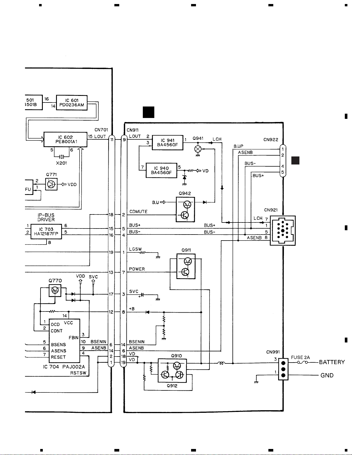
3.3 POWER UNIT
220000/5R5
470/16
470/16
1.4mH
IC940
BA4560F
IC941
BA4560F
HZS4LL(C)
HZS6L(B1)
ERA15-02VH
ERA15-02VH
A
CN701
CN303
F
B
B
POWER UNIT
B
CEK1018
CN911
Page 24

DSP BLOCK
SYSTEM BLOCK
15P
15P
UDZ3R3(B)
UDZ4R7(B)
F
VOICE UNIT
PD6304B(VC,VN)
PD6305B(VS)
24
CDX-P2050VC,P2050VN,P2050VS
1
23
4
1234
D
C
B
A
F
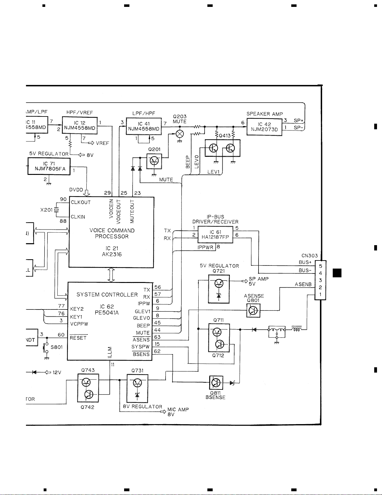
3.4 VOICE UNIT, PCB ASSY
Page 25

AUDIO BLOCK
POWER SUPPLY
BLOCK
SP AMP
100000/5R5
470/16
470/16
and
T
ERA15-02VH
G
PCB ASSY
CN922
B
SW1
SW2
SW3
SW4
SW5
SW6
CN901
CN1
UDZ5R6(B)
CN303
25
CDX-P2050VC,P2050VN,P2050VS
5
6
78
5
6
78
D
C
B
A
F
G
Page 26

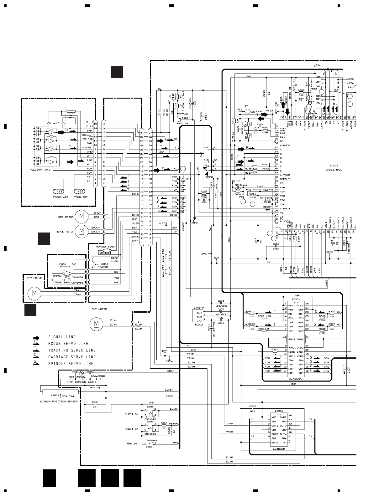
4. PCB CONNECTION DIAGRAM
4.1 CD CORE UNIT
M
M852
ELV
E
F
RERO
EPVO
EREF
IC,Q
ADJ
26
CDX-P2050VC,P2050VN,P2050VS
1
23
4
1234
D
C
B
A
A
SIDE A
CD CORE UNIT
A
NOTE FOR PCB DIAGRAMS
1. The parts mounted on this PCB
include all necessary parts for
several destination.
For further information for
respective destinations, be sure
to check with the schematic diagram.
Capacitor
Connector
P.C.Board
Chip Part
SIDE A
SIDE B
2. Viewpoint of PCB diagrams
CN911
B
C
CN801
Page 27

EJECT
RESET
MAG
IC, Q
27
CDX-P2050VC,P2050VN,P2050VS
D
C
B
A
1
2
34
1
2
34
A
SIDE B
CD CORE UNIT
A
Page 28

1
2
5
6
10
913
14
18
19
28
CDX-P2050VC,P2050VN,P2050VS
1
23
4
1234
D
C
B
A
SIDE A
POWER UNIT
B
CN701
A
CN303
4.2 POWER UNIT
IP-BUS
F
CORD
B
Page 29

29
CDX-P2050VC,P2050VN,P2050VS
D
C
B
A
1
2
34
1
2
34
B
POWER UNIT
B
SIDE B
Page 30

30
CDX-P2050VC,P2050VN,P2050VS
1
23
4
1234
D
C
B
A
D
4.4 SWITCH PCB
SWITCH PCB
D
C
C
4.3 MECHANISM PCB
A
CN101
E
D
MECHANISM PCB
C
M
M854
CRG
M
M851
SPDL
HOME
TRP
DSP
D851
PICKUP UNIT
(SERVICE)
Page 31

31
CDX-P2050VC,P2050VN,P2050VS
D
C
B
A
1
2
34
1
2
34
E
4.5 MOTOR PCB
MOTOR PCB
E
4.6 PCB ASSY
CN1
R6
R4R5
R7
R2
R1
R3
D3
D2
D1
1
5
6
234
CALL
+
VOL
SOURCE
AUDIO
SW1
SW2
SW3
SW4
SW6
SW5
SP
PCB ASSY
G
F
CN901
G
C
Page 32

3
1
2
5
6
4
7
8
8
9
10
11
5
6
7
1
2
3
4
89
10
11
5
67
1
234
CN302
CN301
CN901
1
5
1015
20
22
23
25
30 35
40
44
IC23
1
5
10
15
20
24
25
30
35
40
45
48
IC22
RESET
32
CDX-P2050VC,P2050VN,P2050VS
1
23
4
1234
D
C
B
A
4.7 VOICE UNIT
F
VOICE UNIT
F
CN922
B
SIDE A
CN1
G
Page 33

33
CDX-P2050VC,P2050VN,P2050VS
D
C
B
A
1
2
34
1
2
34
F
VOICE UNIT
F
SIDE B
Page 34

34
CDX-P2050VC,P2050VN,P2050VS
Unit Number : CWX2277
Unit Name : CD Core Unit
MISCELLANEOUS
IC 201 IC UPD63710GC
IC 202 IC BA05FP
IC 301 IC BA5986FM
IC 302 IC LB1836M
IC 501 IC PD4501B
IC 601 IC PD0236AM
IC 602 IC PE8001A1
IC 701 IC PD5512B
IC 702 IC (SRM2B256SLTMX70) GGC1257
IC 703 IC HA12187FP
IC 704 IC PAJ002A
IC 705 IC TC7SH32FU
Q 101 Transistor 2SB1132
Q 701 Transistor DTA144EK
Q 770 Transistor 2SB1184F5
Q 771 Transistor 2SC2412K
D 201 Diode 1SR154-400
D 730 Diode 1SS356
D 770 Diode 1SS355
D 780 Diode 1SS356
L 601 Inductor LCTBR39K2125
X 201 Radiator 16.9344MHz CSS1463
X 701 Ceramic Resonator 10.00MHz CSS1476
S 801 Push Switch(EJECT) CSG1076
S 802 Push Switch(RESET) CSG1076
S 803 Spring Switch(MAG) CSN1044
VR 802 Semi-fixed 680Ω(B) CCP1337
RESISTORS
R 101 RS1/8S120J
R 102 RS1/8S100J
R 103 RS1/16S222J
R 201 RS1/16S104J
R 202 RS1/16S0R0J
R 203 RS1/16S0R0J
R 204 RS1/16S0R0J
R 205 RS1/16S103J
R 206 RS1/16S393J
R 207 RS1/16S182J
R 208 RS1/16S304J
R 212 RS1/16S0R0J
R 213 RS1/16S103J
R 214 RS1/16S103J
R 215 RS1/16S123J
R 216 RS1/16S273J
R 217 RS1/16S273J
R 252 RS1/16S0R0J
R 253 RS1/16S681J
R 254 RS1/16S681J
R 256 RS1/16S681J
R 257 RS1/16S681J
R 258 RS1/16S681J
R 259 RS1/16S102J
R 260 RS1/16S681J
R 298 RS1/16S681J
R 301 RS1/16S103J
R 302 RS1/16S153J
R 303 RS1/16S103J
R 304 RS1/16S153J
R 305 RS1/16S103J
R 306 RS1/16S752J
R 307 RS1/16S103J
R 308 RS1/16S752J
R 309 RA4C332J
R 311 RS1/16S102J
R 501 RS1/16S102J
R 601 RS1/16S102J
R 602 RS1/16S102J
R 603 RS1/16S0R0J
R 604 RA3C681J
R 605 RS1/16S681J
R 606 RS1/16S104J
R 701 RS1/16S681J
R 702 RS1/16S102J
R 703 RS1/16S222J
R 704 RS1/16S104J
R 705 RS1/16S104J
R 706 RS1/16S681J
R 708 RS1/16S0R0J
R 710 RS1/16S473J
R 716 RS1/16S103J
R 717 RS1/16S473J
R 718 RS1/16S681J
R 720 RS1/16S104J
R 721 RS1/16S222J
R 722 RS1/16S222J
R 724 RS1/16S222J
R 725 RS1/16S222J
R 726 RS1/16S104J
R 727 RS1/16S513J
R 729 RS1/16S104J
R 730 RS1/16S473J
R 731 RS1/16S222J
R 732 RS1/16S683J
R 733 RS1/16S222J
R 734 RS1/16S473J
R 735 RS1/16S222J
R 736 RS1/16S103J
R 737 RS1/16S433J
R 738 RS1/16S104J
R 739 RS1/8S1R0J
R 740 RS1/8S2R0J
R 741 RS1/16S102J
R 742 RS1/16S104J
5. ELECTRICAL PARTS LIST
NOTE:
- Parts whose parts numbers are omitted are subject to being not supplied.
- The part numbers shown below indicate chip components.
Chip Resistor
RS1/_S___J,RS1/__S___J
Chip Capacitor (except for CQS.....)
CKS....., CCS....., CSZS.....
=====Circuit Symbol and No.===Part Name Part No.
--- ------ ------------------------------------------ -------------------------
A
=====Circuit Symbol and No.===Part Name Part No.
--- ------ ------------------------------------------ -------------------------
Page 35

R 743 RS1/16S104J
R 744 RS1/16S223J
R 745 RS1/16S104J
R 747 RS1/16S472J
R 748 RS1/16S104J
R 750 RA4C473J
R 751 RA4C473J
R 752 RN1/16SE3602D
R 753 RN1/16SE6801D
R 754 RS1/16S221J
R 755 RS1/16S104J
R 756 RS1/16S221J
R 758 RS1/16S473J
R 759 RS1/16S472J
R 760 RS1/16S104J
R 761 RS1/16S104J
R 768 RS1/8S100J
R 769 RS1/8S100J
R 801 RS1/10S221J
R 802 RS1/10S271J
R 804 RS1/16S512J
R 805 RS1/16S432J
R 806 RS1/16S102J
CAPACITORS
C 101 CKSRYB102K50
C 102 CKSQYB104K25
C 103 CEV101M6R3
C 104 CEV470M6R3
C 105 CKSQYB334K16
C 106 CKSQYB334K16
C 107 CKSQYB334K16
C 201 CKSQYB104K25
C 202 CEV101M6R3
C 203 CKSQYB104K25
C 204 CKSRYB332K50
C 205 CKSQYB104K25
C 206 CKSRYB392K50
C 207 CKSQYB224K16
C 208 CCSRCH270J50
C 209 CCSRCJ3R0C50
C 210 CCSRCH221J50
C 211 CCSRCH101J50
C 212 CKSRYB682K50
C 213 CKSQYB104K25
C 214 CKSQYB104K25
C 215 CKSQYB104K25
C 216 CKSQYB104K25
C 217 CKSQYB104K25
C 218 CKSQYB104K25
C 219 CKSQYB104K25
C 220 CKSQYB104K25
C 253 CKSRYB471K50
C 271 CEV101M6R3
C 272 22µF/6.3V CCH1300
C 273 CKSQYB334K16
C 301 CEV101M10
C 302 CKSQYB224K16
C 501 CKSRYB104K16
C 502 CKSRYB471K50
C 601 CKSRYB104K16
C 602 CKSRYB104K16
C 603 CKSRYB104K16
C 604 CSZSR100M16
C 605 CKSRYB104K16
C 606 CKSRYB104K16
C 607 CEV101M6R3
C 608 CSZSR100M16
C 609 CCSRCH180J50
C 610 CCSRCH180J50
C 611 CKSRYB104K16
C 612 CCSRCH102J50
C 613 CCSRCH102J50
C 701 CKSRYB103K25
C 702 CKSQYB473K16
C 703 CKSQYB473K16
C 707 CKSRYB103K25
C 708 CKSQYB104K25
C 710 CKSRYB103K25
C 711 CKSRYB102K50
C 712 CKSRYB102K50
C 714 CKSQYB104K25
C 715 CSZST220M16
C 717 CKSRYB103K25
C 718 CKSRYB103K25
C 719 CKSRYB102K50
C 720 CKSRYB102K50
C 721 CKSRYB103K25
C 722 CKSRYB103K25
C 723 CKSRYB471K50
C 801 CKSRYB103K25
C 802 CKSQYB104K25
C 803 CKSRYB103K25
Unit Number : CWM6365
Unit Name : Power Unit
MISCELLANEOUS
IC 940 IC BA4560F
IC 941 IC BA4560F
Q 910 Transistor 2SD2396
Q 911 Transistor IMD2A
Q 912 Transistor IMX1
Q 941 Transistor FMG12
Q 942 Transistor IMD2A
D 901 Diode ERA15-02VH
D 902 Diode ERA15-02VH
D 910 Diode HZS6L(B1)
D 941 Diode MA152WA
D 942 Diode HZS4LL(C)
L 901 Choke Coil 1.4mH CTH1129
RESISTORS
R 901 RS1/10S204J
R 902 RS1/10S104J
R 910 RS1/8S431J
R 911 RS1/10S681J
R 912 RS1/8S101J
R 913 RS1/10S512J
R 914 RS1/10S132J
R 915 RD1/4PU151J
R 921 RS1/10S101J
R 922 RS1/10S101J
R 923 RS1/10S102J
R 924 RS1/10S473J
R 941 RS1/10S102J
R 942 RS1/10S102J
R 943 RS1/10S183J
R 944 RS1/10S183J
R 945 RS1/10S222J
R 946 RS1/10S562J
R 947 RS1/10S472J
R 948 RS1/10S472J
R 949 RS1/10S562J
R 950 RS1/10S562J
R 951 RS1/10S0R0J
R 952 RS1/10S562J
R 953 RS1/10S562J
35
CDX-P2050VC,P2050VN,P2050VS
=====Circuit Symbol and No.===Part Name Part No.
--- ------ ------------------------------------------ -------------------------
=====Circuit Symbol and No.===Part Name Part No.
--- ------ ------------------------------------------ -------------------------
B
Page 36

36
CDX-P2050VC,P2050VN,P2050VS
R 954 RS1/10S101J
CAPACITORS
C 901 CKSQYB104K50
C 902 470µF/16V CCH1183
C 903 CKSQYB223K25
C 904 470µF/16V CCH1183
C 906 0.22F/5.5V CCL1037
C 907 CCSQCH101J50
C 910 CKSQYB103K50
C 911 CKSQYB103K50
C 912 CEJA220M10
C 913 CKSQYB103K50
C 941 CEJA100M16
C 942 CEJA100M16
C 943 CEAL100M16
C 944 CEAL100M16
C 945 CEAL100M16
C 947 CEAL101M10
C 948 CKSQYB103K50
C 949 CKLSQB152K50
C 950 CKLSQB152K50
C 951 CCSQCH331J50
C 952 CCSQCH331J50
C 953 CEAL100M16
Unit Number : CWM6367(VC,VN)
: CWM6366(VS)
Unit Name : Voice Unit
MISCELLANEOUS
IC 11 IC NJM4558MD
IC 12 IC NJM4558MD
IC 21 IC AK2316
IC 22 IC (VC,VN model) PD6304B
IC 22 IC (VS model) PD6305B
IC 23 IC
M5M51016BTP-70LL
IC 41 IC NJM4558MD
IC 42 IC NJM2073D
IC 61 IC HA12187FP
IC 62 IC PE5041A
IC 71 IC NJM7805FA
IC 82 IC S-80730ANDT
Q 201 Transistor DTA114EK
Q 203 Transistor DTC114TK
Q 413 Transistor IMH11A
Q 711 Transistor 2SB1238
Q 712 Transistor DTC143EK
Q 721 Transistor 2SD1859
Q 731 Transistor 2SD1859
Q 742 Transistor DTC143EK
Q 743 Transistor 2SB1238
Q 751 Transistor 2SB1238
Q 752 Transistor DTC143EK
Q 801 Transistor DTC114TK
Q 811 Transistor 2SC2412K
Q 821 Transistor 2SD1760F5
D 101 Diode UDZ3R3(B)
D 141 Diode UDZ4R7(B)
D 201 Chip Diode MA151WK
D 702 Diode ERA15-02VH
D 711 Diode UDZ5R6(B)
D 731 Diode HZS9L(C1)
D 761 Diode HZ30P
D 811 Diode HZS7L(C2)
D 821 Diode ERA15-02VH
D 822 Diode HZS6L(C2)
D 823 Diode 1SS356
D 824 Diode 1SS356
D 831 Diode 1SS356
L 101 Ferri-Inductor LAU101K
L 102 Inductor LCTBR47K2125
L 241 Inductor LCTBR47K2125
L 251 Inductor LCTBR47K2125
L 261 Inductor LCTBR47K2125
L 631 Inductor LCTBR47K2125
L 651 Inductor LCTBR47K2125
L 671 Inductor CTF1295
L 672 Inductor LCTBR47K2125
L 673 Inductor LCTBR47K2125
L 701 Choke Coil 1.4mH CTH1129
X 201 Crystal Resonator 12.288MHz CSS1378
X 631 Radiator 6.290MHz CSS1451
S 801 Switch(RESET) CSG1059
EF 701 EMI Filter CCG1003
RESISTORS
R 101 RS1/10S681J
R 102 RS1/10S821J
R 103 RS1/10S102J
R 111 RS1/10S153J
R 112 RS1/10S102J
R 113 RS1/10S103J
R 121 RS1/10S682J
R 122 RS1/10S124J
R 123 RS1/10S152J
R 131 RS1/10S272J
R 132 RS1/10S333J
R 141 RS1/10S472J
R 201 RA4C220J
R 202 RA4C220J
R 203 RA4C220J
R 204 RA4C220J
R 205 RA4C220J
R 206 RA4C220J
R 207 RA4C220J
R 208 RA4C220J
R 209 RA4C220J
R 210 RS1/16S220J
R 211 RS1/16S0R0J
R 212 RS1/16S105J
R 213 RS1/16S0R0J
R 217 RS1/16S220J
R 220 RS1/16S472J
R 221 RS1/16S472J
R 222 RS1/16S472J
R 223 RS1/16S472J
R 231 RA4C220J
R 232 RA4C220J
R 233 RA4C220J
R 234 RA4C220J
R 241 RS1/16S472J
R 242 RS1/16S472J
R 243 RS1/16S472J
R 251 RS1/16S0R0J
R 271 RS1/10S472J
R 272 RS1/10S472J
R 401 RS1/10S103J
R 402 RS1/10S103J
R 403 RS1/10S103J
R 411 RS1/10S473J
R 412 RS1/10S473J
=====Circuit Symbol and No.===Part Name Part No.
--- ------ ------------------------------------------ -------------------------
=====Circuit Symbol and No.===Part Name Part No.
--- ------ ------------------------------------------ -------------------------
F
Page 37

R 413 RS1/10S681J
R 417 RS1/10S0R0J
R 421 RS1/10S102J
R 422 RS1/10S302J
R 423 RS1/10S102J
R 424 RS1/10S682J
R 425 RS1/10S392J
R 431 RS1/10S104J
R 433 RS1/10S103J
R 451 RS1/10S271J
R 452 RS1/10S332J
R 453 RS1/10S332J
R 454 RS1/10S100J
R 603 RS1/16S104J
R 632 RS1/16S104J
R 634 RS1/16S104J
R 635 RS1/16S104J
R 636 RS1/16S103J
R 637 RS1/16S101J
R 638 RS1/16S103J
R 639 RS1/16S101J
R 640 RS1/16S104J
R 650 RS1/16S122J
R 651 RS1/16S101J
R 652 RS1/16S101J
R 653 RS1/16S473J
R 654 RS1/16S473J
R 711 RS1/10S103J
R 712 RS1/10S122J
R 721 RD1/4PU471J
R 731 RS1/10S331J
R 741 RS1/10S222J
R 743 RS1/10S103J
R 751 RS1/10S103J
R 752 RS1/10S222J
R 761 RS2PMF180J
R 801 RS1/10S822J
R 802 RS1/10S104J
R 811 RS1/10S473J
R 812 RS1/10S223J
R 821 RS1/10S101J
R 822 RS1/10S472J
R 831 RS1/10S101J
R 832 RS1/10S104J
R 834 RS1/10S102J
R 835 RD1/4PU102J
CAPACITORS
C 101 CEAL101M10
C 102 CCSQCH101J50
C 103 CCSQCH101J50
C 111 CEJAR22M50
C 113 CKSQYB152K50
C 121 CKSQYB154K16
C 122 CKSQYB154K16
C 123 CKSQYB154K16
C 124 CEAL470M16
C 131 CKSQYB474K16
C 132 CCSQCH560J50
C 133 CEJAR68M50
C 141 CKSQYB103K50
C 142 CEAL470M16
C 201 CKSQYB105K16
C 202 CEJA100M16
C 203 CKSQYB105K16
C 204 CEJA100M16
C 205 CKSRYB103K50
C 206 CKSYB684K16
C 208 CCSRCH150J50
C 209 CCSRCH150J50
C 210 CKSRYB103K50
C 211 CKSQYB105K16
C 220 CEJA220M16
C 241 CEJA220M16
C 242 CKSQYB105K16
C 244 CKSQYB105K16
C 245 CCSRCH101J50
C 251 CKSQYB105K16
C 261 CKSQYB105K16
C 263 CKSQYB102K50
C 304 CKSRYB102K50
C 402 CKSQYB332K50
C 403 CKSQYB682K50
C 411 CKSQYB223K50
C 412 CKSQYB123K50
C 413 CKSQYB103K50
C 414 CKSQYB105K16
C 421 CKSQYB105K16
C 431 CKSQYB103K50
C 432 CKSQYB103K50
C 451 CKSQYB223K50
C 452 CKSQYB223K50
C 453 CEJA1R0M50
C 454 CEJA1R0M50
C 455 CEAL101M10
C 456 CKSQYB104K50
C 457 CKSQYB473K50
C 631 CKSRYB104K16
C 651 CKSRYB471K50
C 652 CKSRYB471K50
C 653 CKSRYB102K50
C 654 CKSRYB102K50
C 655 CKSQYB104K50
C 671 CCSRCH101J50
C 672 CKSRYB102K50
C 673 CKSRYB102K50
C 702 470µF/16V CCH1183
C 703 CKSQYB102K50
C 704 470µF/16V CCH1183
C 706 CKSQYB102K50
C 711 CEAS331M16
C 721 CEAL470M16
C 722 CEAL101M10
C 731 CEAL470M16
C 732 CEAL101M10
C 743 CEAL101M10
C 761 CKSQYB104K50
C 763 CKSQYB224K16
C 801 CKSQYB223K50
C 821 CEAL470M16
C 822 CKSQYB103K50
C 831 CEJA221M6R3
C 832 CEJA1R0M50
C 833 CKSQYB104K50
C 842 0.1F/5.5V CCL1023
C 851 CSZA220M16
37
CDX-P2050VC,P2050VN,P2050VS
=====Circuit Symbol and No.===Part Name Part No.
--- ------ ------------------------------------------ -------------------------
=====Circuit Symbol and No.===Part Name Part No.
--- ------ ------------------------------------------ -------------------------
Page 38

Unit Number :
Unit Name : Mechanism PCB
Q 851 Photo-transistor PT4800
S 853 Spring Switch(HOME) CSN1051
Unit Number :
Unit Name : Switch PCB
D 851 LED CN504-2
S 851 Spring Switch(DSP) CSN1051
S 852 Spring Switch(TAP) CSN1052
Unit Number :
Unit Name : Motor PCB
M 853 Motor(TRAY) CXB4421
Unit Number : MWM1073
Unit Name : PCB Assy
MISCELLANEOUS
D 1 LED SLR-332MC(MN)
D 2 LED SLR-332MC(MN)
D 3 LED SLR-332MC(MN)
SW 1 Switch(CALL) CSG1044
SW 2 Switch(+) CSG1044
SW 3 Switch(-) CSG1044
SW 4 Switch(VOL) CSG1044
SW 5 Switch(AUDIO) CSG1044
SW 6 Switch(SOURCE) CSG1044
RESISTORS
R 1 RD1/4PU100J
R 2 RD1/4PU472J
R 3 RD1/4PU153J
R 4 RD1/4PU100J
R 5 RD1/4PU472J
R 6 RD1/4PU153J
R 7 RD1/4PU151J
Miscellaneous Parts List
Pickup Unit(P8)(Service) CXX1285
M 851 Motor(SPINDLE) CXB3003
M 852 Motor(ELV) CXB3006
M 854 Motor(CARRIAGE) CXB3004
VR 801 Volume 10K CCW1024
38
CDX-P2050VC,P2050VN,P2050VS
=====Circuit Symbol and No.===Part Name Part No.
--- ------ ------------------------------------------ -------------------------
C
D
E
G
Page 39

39
CDX-P2050VC,P2050VN,P2050VS
• Note :
CD mechanism modules the grating angle of the pickup unit cannot be adjusted after the pickup unit is changed.
The pickup unit in the CD mechanism module is adjusted on the production line to match the CD mechanism
module and is thus the best adjusted pickup unit for the CD mechanism module. Changing the pickup unit is thus
best considered as a last resort. However, if the pickup unit must be changed, the grating should be checked
using the procedure below.
• Purpose :
To check that the grating is within an acceptable range.
• Symptoms of Mal-adjustment :
If the grating is off by a large amount symptoms such as being unable to close tracking, being unable to perform
track search operations, or track searching taking a long time, may appear.
• Method :
• Measuring Equipment • Oscilloscope, Two L.P.F.
• Measuring Points • E, F, REFO
• Disc • ABEX TCD-784
• Mode • TEST MODE
• Checking Procedure
1. Enter Test mode, then select Multi-CD player and switch the 5V regulator on.
2. Using the TRK+ and TRK- buttons, move the pickup unit to the innermost track.
3. Press key 9 to close focus, the display should read "91". Press key 9 2 times. Enter Rough Servo mode. Press key
8 to implement the tracking balance adjustment the display should now read "81".
4. As shown in the diagram above, monitor the LPF outputs using the oscilloscope and check that the phase difference is within 75° . Refer to the photographs supplied to determine the phase angle.
5. If the phase difference is determined to be greater than 75° try changing the pickup unit to see if there is any
improvement. If, after trying this a number of times, the grating angle does not become less than 75° then the
mechanism should be judged to be at fault.
• Note
Because of eccentricity in the disc and a slight misalignment of the clamping center the grating waveform may be
seen to "wobble" ( the phase difference changes as the disc rotates). The angle specified above indicates the average angle.
• Hint
Change the disc changes the clamp position and may decrease the "wobble".
REFO
E
F
E
F
L.P.F.
L.P.F.
CD CORE UNIT
Xch
Ych
Oscilloscope
100kΩ
100kΩ
390pF
390pF
6.1 CHECKING THE GRATING
- Checking the Grating After Changing the Pickup Unit
6. ADJUSTMENT
Page 40

40
CDX-P2050VC,P2050VN,P2050VS
Grating waveform
45˚
0˚
75˚
60˚
30˚
90˚
Echt Xch 20mV/div, AC
Fcht Ych 20mV/div, AC
Page 41

41
CDX-P2050VC,P2050VN,P2050VS
• Note :
This mechanisms is detects the height of the stage using slide-variable resistance.
To absorb dislocation of the stage height caused by differences in the mechanism and the CD core unit, adjustment
must be made for each CD-mechanism module using a variable resistor.
Normally, readjustment is not needed, as this has been adjusted at the factory. However, adjustment of elevation is
required according to the procedure explained below if an elevation error has occurred or if the CD core unit has
been removed.
• Purpose :
To adjust and confirm whether or not elevation operates correctly.
• Adjustment Method :
• Measuring Equlpment: Oscilloscope, One L.P.F.
• Measuring Points : EREF, EPVO
• Setting : Without a magazine in Test mode
With the mechanism placed upside-down (Place the CD mechanism module so that the CD
core unit is above.)
• Confirmation Procedure
1. Enter Test mode, then select Multi-CD player.
2. Press key 7 to enter Mechanism Test mode.
3. Press key 12 twice to specify the amount of movement.
6.2 ADJUSTMENT OF ELEVATION WHEN THE CD CORE UNIT HAS BEEN REMOVED
FOR MAINTENANCE
- Adjustment When Error Code 60 is Displayed Because of Malfunctioning Elevation
TRACK FUNCTION
'"
TRACK FUNCTION
72 00' 00"
EREF
EPVO
Oscilloscope
CD CORE UNIT
L.P.F.
47kΩ
1µF
Examples of display
TRACK FUNCTION
72 00' 02"
TRACK FUNCTION
72 00' 01"
The amount of movement
changes each time key 12 is
pressed.
maximum movement
i
Key 12
i
during movement
i
Key 12
i
minimum movement
TRACK FUNCTION
72 00' 00"
i
i
Key 12
Page 42

42
CDX-P2050VC,P2050VN,P2050VS
4. Press key 9 to set ELV/TRAY mode to TRAY.
5. Press key FF to release the clamp and return the tray to the magazine.
6. Press key 9 to enter Elevation Move mode.
7. Use key FF/REV to operate elevation and set if to the graduation of the sixth step
(Fig. 1).
8. Make the adjustment.
Use VR802 to adjust the difference in potential between EREF and EPVO to 0 ±10
mV.
9. When adjustment is completed, press key BAND to exit Mechanism Test mode.
10. Confirm operation of the mechanism.
Place the mechanism horizontally (CD core unit below). Take care not to short-circuit the PCB.
11. Confirm the height of the stage. Use the DISC± key to select Disc No.6.
Check if the stopper bend of the clamp lever is engaged in the groove of the frame
stopper (Fig. 2-4).
• Note :
The stopper bend will be pressed downward into the groove for final clamping. Confirm the engagement position
of the stopper bend.
• If the stopper bend is engaged in the center and pressed downward, adjustment is completed. Go to step 15.
• If the stopper bend is dislocated, check the amount of dislocation by following steps 12 to 14.
TRACK FUNCTION
72 00' 02"
TRACK FUNCTION
72 00' 02"
TRACK FUNCTION
'"
TRACK FUNCTION
04 00' 00"
Examples of display
TRACK FUNCTION
72 01' 02"
Release the clamp
Page 43

43
CDX-P2050VC,P2050VN,P2050VS
12. To see the amount of dislocation, place the mechanism upside-down.
If the stopper bend has been dislocated in the direction of the first
CD, turn VR802 to the left(Fig. 2).
To lower the stage toward the twelfth step by 0.1 mm, reduce the
voltage of EREF (adjusted in step 8) by 10 mV.
If the stopper bend has been dislocated in the direction of the twelfth
CD, turn VR802 to the right(Fig. 4).
To raise the stage toward the first step by 0.1 mm, increase the voltage of EREF (adjusted in step 8) by 10 mV.
13. Place the mechanism horizontal. Go back to step 11 to reconfirm the
stage height.
14. When adjustment of the stage height is completed, proceed as follows:
15. Press the EJECT switch.
16. Once operation of the mechanism has stopped, turn the power OFF.
17. Wait more than one minute after the power is turned off, then turn the power ON and insert a magazine.
18. Check if the mechanism operates correctly with the first, sixth, seventh and twelfth CDs.
19. If the mechanism operates properly, adjustment is completed. If the mechanism operates improperly, make the
adjustment again.
GND
EREF
VR802
1µF
47kΩ
Oscilloscope
L.P.F.
Page 44

44
CDX-P2050VC,P2050VN,P2050VS
NG
Stopper bend of the
clamp lever
Frame stopper
OK
Engaged in the center and pressed downward.
NG
Fig. 1
Dislocated toward the first CD.
Adjust the insertion gate of magazine to
the sixth scale.
Dislocated toward the twelfth CD.
Fig. 2
Fig. 3
Fig. 4
E
12346 5789BC
Page 45

1) Precautions
• This unit uses a single power supply (+5V) for the regulator. The signal reference potential, therefore, is
connected to REFO(approx. 2.5V) instead of GND.
If REFO and GND are connected to each other by mistake during adjustments, not only will it be impossible to measure the potential correctly, but the servo
will malfunction and a severe shock will be applied to
the pick-up. To avoid this, take special note of the following.
Do not connect the negative probe of the measuring
equipment to REFO and GND together. It is especially
important not to connect the channel 1 negative
probe of the oscilloscope to REFO with the channel 2
negative probe connected to GND.
Since the frame of the measuring instrument is usually at the same potential as the negative probe, change
the frame of the measuring instrument to floating status.
If by accident REFO comes in contact with GND,
immediately switch the regulator or power OFF.
• Always make sure the regulator is OFF when connecting and disconnecting the various filters and wiring
required for measurements.
• Before proceeding to further adjustments and measurements after switching regulator ON, let the player
run for about one minute to allow the circuits to stabilize.
• Since the protective systems in the unit's software are
rendered inoperative in test mode, be very careful to
avoid mechanical and /or electrical shocks to the system when making adjustment.
• Disc detection during tray extraction and return operations is performed by means of the photo transistor
in this unit. Consequently, if the inside of the unit is
exposed to a strong light source with the outer casing
removed for repairs or adjustment, the following malfunctions may occur:
*Even with a disc loaded, the unit detects "no disc"
and cannot start play.
*Although a 12-cm disc is loaded, the unit detects
"8cm disc" mistakenly.
When the unit malfunctions this way, either re-position the light source, move the unit or cover the photo
transistor.
• During exchanging discs, do not press the keys for
the discs to be exchanged.
2) Test Mode
This mode is used for adjusting the CD mechanism
module of the device.
• Test mode starting procedure
Reset while pressing the 4 and 6 keys together.
• Test mode cancellation
Switch ACC, back-up OFF.
• If the 8 or 9 key is pressed while focus search is in
progress, immediately turn the power off (otherwise
the actuator may be damaged due to the lens stuck).
• Jump operation of TRs other than 100TR continues
after releasing the key. CRG move and 100TR jump
operations are brought into the “Tracking close” status when the key is released.
• Powering Off/On resets the jump mode to “Single TR
(91)”, the RF AMP gain setting to 0 dB, and the automatic adjustment value to the initial value.
• During exchanging discs, do not press the keys for
the discs to be exchanged.
Key to adjustment text HEAD UNIT (6 keys type)
inside (12 keys type)
BAND BAND
TRK+/FF TRK+/FF
TRK-/REV TRK-/REV
71
82
93
10 4
11 5
12 6
DISC- DISCSOURCE ON/OFF SOURCE ON/OFF
45
CDX-P2050VC,P2050VN,P2050VS
7. GENERAL INFORMATION
7.1 DIAGNOSIS
7.1.1 TEST MODE
- CD Test Mode
Page 46

Focus Close*2S Curve Check
01 01 0100 00 00
(99 99 99)
Display
TYP
4
9
Reset
SOURCE
New test mode
6
TRK-
BAND
9
*2
*1
+6dB +12dB
*4
*5
12
12
12
12
7
8
7
8TRK+
TRK+ TRK-
06 06 06 12 12 12
Sourse CD
Single TR
9x(8x):91(81)
32TRK
92(82)
CRG Move
94(84)
100TRK
93(83)
Focus Mode
Select
Focus Close/
S Curve Check
CRG−
Auto Adjustment
Display Select
<Tracking Servo Close> CRG+
RF AGC Coefficient Display/
Rough Servo and RF AGC
Tracking
Open
Display
Tracking
Open
T. Close and
Fit Servo
*3 F.Offset Display RF.Offset Display F.Cansel Display
*7
Single TR/32TR/100TR
Voltage of CRG Motor = 2 [V]
(F,T.AGC Gain = (Present Value/Initial Value) × 20)
*6
TRK+ TRK-
7
9
Display
8
9
Display
or
8x 8x 8x
TRK SECMIN
9x 9x 9x
TRK SECMIN
or
CRG−CRG+
T.Balance
Adjustment
*7
F, T, RF AGC/
F.Bias Display Select
F, T AGC and
RF AGC
CRG Move, 100TR Jump Only
TRK, MIN, SEC F.AGC Gain
RF AGC Gain
T.AGC Gain
*8
Power ON
(Adjustment for T.Offset)
*5
*4 *4
*6
CRG/TR Jump NO.
Select
CRG+/TR Jump+
CRG−/TR Jump−
Power OFF
Display
Display
Display
T.Close and
F,T AGC and
RF AGC and
Fit Servo
Display
Power ON
(Not adjustment for T.Offset)
Display
Display
8
RF AMP Gain Select
8
Power OFF
Power OFF
Power OFF
8x 8x 8x
TRK SECMIN
9x 9x 9x
TRK SECMIN
8x 8x 8x
TRK SECMIN
9x 9x 9x
TRK SECMIN
or
8x 8x 8x
TRK SECMIN
9x 9x 9x
TRK SECMIN
or
00 00 00
TRK SECMIN
99 99 99
TRK SECMIN
or
00 00 00
TRK SECMIN
99 99 99
TRK SECMIN
or
00 00 00
TRK SECMIN
99 99 99
TRK SECMIN
or
91 91 91
TRK SECMIN
0x 0x 0x
TRK SECMIN
00 00 00
TRK SECMIN
99 99 99
TRK SECMIN
GG GG GG
TRK SECMIN
Test Mode In
*1
*8 *3*8
F.Cancel Value = {Top Rank 8bit of Set Value (7F [H] to 80 [H] ) + 128} / 4
= 63 [D] to (32 [D] ) to 00 [D]
BAND
BAND
BAND
BAND
912FF7REV BAND
Display
< Mechanism test mode in >
Display
<ELV,TRAY select>
<Operation mode
select >
<Shift > <Shift >
*9 *12*11*10
<Mechanism test
mode out >
72 00 00
TRK SECMIN
TRK SECMIN
0X0072
*9 ELV motor select
*10
Display
TRAY motor select
0X1072
000072 010072 020072
8ms pulse drive
Display
24ms pulse drive DC drive
*11
001072
011072 021072
48ms pulse drive
Display
100ms pulse drive DC drive
ELV select : ELV dowm (Disc 12
→ 1)
TRAY select : TRAY out
*12 ELV select : ELV up (Disc 1
→ 12)
TRAY select : TRAY in
46
CDX-P2050VC,P2050VN,P2050VS
- Flow Chart
Page 47

47
CDX-P2050VC,P2050VN,P2050VS
- Error Messages
If a CD is not operative or stopped during operation due to an error, the error mode is turned on and cause(s) of the
error is indicated with a corresponding number. This arrangement is intended at reducing nonsense calls from the
users and also for facilitating trouble analysis and repair work in servicing.
(1) Basic Indication Method
1) When SERRORM is selected for the CSMOD (CD mode area for the system), error codes are written to DMIN (minutes display area) and DSEC (seconds display area). The same data is written to DMIN and DSEC. DTNO remains
in blank as before.
2) Head unit display examples
Depending on display capability of LCD used, display will vary as shown below. xx contains the error number.
8-digit display 6-digit display 4-digit display
ERROR–xx ERR–xx E–xx
OR
Err–xx
* When the system is manufactured for an OEM basis, the error display will be configured according to the customer
specification.
(2) Error Code List
Code Class Displayed error code Description of the code and potential cause(s)
10 Electricity Carriage Home NG CRG can't be moved to inner diameter.
CRG can't be moved from inner diameter.
→ Failure on home switch or CRG move mechanism.
11 Electricity Focus Servo NG Focusing not available.
→ Stains on rear side of disc or excessive vibrations on REWRITABLE.
12 Electricity Spindle Lock NG Spindle not locked. Sub-code is strange (not readable).
→ Failure on spindle, stains or damages on disc, or excessive vibrations.
Subcode NG A disc not containing CD-R data is found. Turned over disc are found,
though rarely.
→ Failure on home switch or CRG move mechanism.
RF AMP NG An appropriate RF AMP gain can't be determined.
→ CD signal error.
17 Electricity Setup NG APC protection doesn't work. Focus can be easily lost.
→ Damages or stains on disc, or excessive vibrations.
30 Electricity Search Time Out Failed to reach target address.
→ CRG tracking error or damages on disc.
A0 System Power Supply NG Power (VD) is ground faulted.
→ Failure on SW transistor or power supply (failure on connector).
A1 System Mechanism power Mechanism elevation reference voltage is out of
failure prescription.
→EREF adjustment VR and/or power abnormal.
50 Mecha- An error upon MAG switch release time has time out.
nism ejection Elevation time out when eject.
60 Mecha- An error while putti- Tray in / out time has time out.
nism ng in and out the tray Tray is caught when put in.
Page 48

48
CDX-P2050VC,P2050VN,P2050VS
Code Class Displayed error code Description of the code and potential cause(s)
70 Mecha- An error upon Elevation time has time out.
nism elevation
80 Mecha- An error with an em- No disc is available.
nism pty magazine inserted
Remarks: Unreadable TOC does not constitute an error. An intended operation continues in this case.
A newly designed head unit must conform to the example given above.
Upper digits of an error code are subdivided as shown below:
1x: Setup relevant errors, 3x: Search relevant errors, 3x: Search relevant errors, Ax: Other errors.
- New Test Mode
M-CD plays the same way as before.
If an error such as off focus, spindle unlocking, unreadable sub-code, or sound skipping occurs after setup, its
cause and time occurred (in absolute time) are displayed.
During setup, operational status of the control software (internal RAM: CPOINT) is displayed.
These displays and functions are prepared for enhancing aging in the servicing and efficiency of trouble analysis.
(1) Shifting to the New Test Mode
1 Turn on the current test mode by starting the reset from the 4 and 6 keys together.
2 Select M-CD for the source through the specified procedure including use of the [SOURCE] key. Then, press the
12 key while maintaining the regulator turned off.
3 After the above operations, the new test mode remains on irrespective of whether the M-CD is turned on or off.
You can reset the new test mode by turning on the reset start.
* With some products, the new test mode can be reset through the same operations as that employed for shifting to
the STBY mode (while maintaining the Acc turned off).
(2) Key Correspondence
Key Test mode New test mode
(Example) Power Off Power On In-play Error Production
BAND To power on To power off – Time/Err.No. switching
(offset adjustment performed)
UP – FWD-Kick FF/TR+ –
DOWN – REV-Kick REV/TR- –
7 – T.Close (AGC performed) Scan –
/parameter display switching
8 RF AMP gain switching Parameter display switching Mode –
/T.BAL adjustment/T.Open
9 To power on F.Close/RF AGC/F.T.AGC – –
(offset adjustment not performed)
10 – F.Open – –
11 – Jump Off – –
12 – F.Mode switching Auto/Manu T.No./Time switching
/T.Close (no AGC)/Jump switching
Page 49

49
CDX-P2050VC,P2050VN,P2050VS
Key Mechanism Test Mode
(Example)
BAND Back to the test mode
UP Playing the mechanism
DOWN Playing the mechanism
7 Mechanism test mode in
8–
9 TRAY/ELV select
10 –
11 –
12 Operation step select
Note: Eject and CD on/off is performed in the same procedure as that for the normal mode.
(3) Cause of Error and Error Code
Code Class Contents Description and cause
40 Electricity Off focus detected. FOK goes low.
→ Damages/stains on disc, vibrations or failure on servo.
41 Electricity Spindle unlocked. FOK = Low continued for 50 msec.
→ Damages/stains on disc, vibrations or failure on servo.
42 Electricity Sub-code unreadable. Sub-code was unreadable for 50 msec.
→ Damages/stains on disc, vibrations or failure on servo.
43 Electricity Sound skipping detected. Last address memory function was activated.
→ Damages/stains on disc, vibrations or failure on servo.
Note: Mechanical errors during aging are not displayed.
The error codes should be indicated in the same way as in the normal mode.
(4) Display of Operational Status (CPOINT) during Setup
Status No. Contents Protective action
00 CD+5V ON process in progress. None
01 Servo LSI initialization (1/3) in progress. None
02 Servo LSI CRAM initialization in progress. None
03 Servo LSI initialization (2/3) in progress. None
04 Offset adjustment (1/3) in progress. None
05 Offset adjustment (2/3) in progress. None
06 Offset adjustment (3/3) in progress. None
07 FZD adjustment in progress. None
08 Servo LSI initialization (3/3) in progress. None
10 Carriage move to home position started. None
11 Carriage move to home position started. None
12 Carriage is moving toward inner diameter. Specified 10 seconds has been passed or failure
on home switch.
13 Carriage is moving toward outer diameter. Specified 10 seconds has been passed or failure
on home switch.
14 Carriage outer kick in progress. None
15 Carriage outer diameter feed (1 second) in progress. None
20 Servo close started. None
21 Pre-processing for focus search started. None
22 Spindle rotation and focus search started. None
23 Waiting for focus close (XSI=Low). Specified focus search time has been passed.
24 Standing by after focus close is over. Specified focus search time has been passed.
25 Focus search preprocessing is in None
progress while setup protection is turned on.
Page 50

50
CDX-P2050VC,P2050VN,P2050VS
Status No. Contents Protective action
26 Focus search preprocessing is in None
progress while focus recovery is turned on.
27 Wait time after focus close is set up. Off focus.
28 Standing by after focus close is over. Off focus.
29 Setup (1/2) before T balance adjustment is started. Off focus.
30 Setup (2/2) before T balance adjustment is started. Off focus.
31 T balance adjustment started. Off focus.
32 T balance adjustment (1/2). Off focus.
33 T balance adjustment (2/2). Off focus.
34 Waiting for spindle rotation to end. Off focus.
Spindle rough servo.
35 Standing by after spindle rough servo is over. Off focus.
36 RF AGC started. Off focus.
37 RF AGC started. Off focus.
38 RF AGC ending process in progress. Off focus.
39 Tracking close in progress. Off focus.
40 Standing by after tracking is closed. Off focus.
Carriage closing in progress.
41 Focus/tracking AGC started. Off focus.
42 Focus AGC started. Off focus.
43 Focus AGC in progress. Off focus.
44 Tracking AGC in progress. Off focus.
45 Standing by after focus/tracking AGC are over. Off focus.
46 Spindle processes applicable servo. Off focus.
47 Check for servo close is started. Off focus.
48 Check of LOCK pin started. Off focus or spindle not locked.
49 RF AGC started. Off focus.
50 RF AGC in progress. Off focus.
51 Standing by after RF AGC is over. Off focus.
(5) Display Examples
1) During Setup (When status no. = 11)
TRK No. MIN. SEC.
11 11' 11"
2) During Operation (TOC read, TRK search, Play, FF and REV)
The same as in the normal mode.
3) When a Protection Error Occurred
Switch to the following displays (A) and (B) using the [BAND] switch:
(A) Error occurrence timing display in absolute time.
An example: Error occurred in 12th tune at 34'56" in absolute time.
TRK No. MIN. SEC.
12 34' 56"
(B) Error No. display
An example: Error #40 (Off focus is detected)
ERROR-40
Page 51

51
CDX-P2050VC,P2050VN,P2050VS
- VOICE UNIT Test Mode
Step 1: Turning on the test mode
1 Connect Pin 1 on the microcomputer to the ground, supply power, then press the reset switch.
2 At this time, the automatic self-check is implemented by the voice recognition LSI (AK2316).
When normal: The “Test mode” guidance will be output.
If any trouble is present: The following frequency of “pee” sounds will be repeated depending on type of the
given error. When this sound is ended, you can repeat the “pee” sounds all over again by pressing any key.
If the self-check detected any error, you can’t proceed to further steps in the test mode. Return to the selfcheck 1 above.
<Frequency of “pee” sounds and the corresponding error content>
3 times: Error A is detected.
4 times: Error B is detected.
5 times: Errors A and B are detected.
6 times: Error D is detected.
7 times: Errors A and D are detected.
8 times: Errors B and D are detected.
9 times: Errors A, B and D are detected.
Where,
A: Flash memory (static data area) check-sum error.
B: Communication error between DSP and RISC.
D: External SRAM write/read error.
* For details of the voice recognition specification, refer to the specification for the voice recognition LSI
(AK2316).
Step 2: Generating output of the built-in guidance word by word using the “+ key” or “- key”.
1 Press the “+ key” or “- key”.
2 This will output one word of the guidance. For the guidance list, refer to the “List of Guidance by
Destination” (see page 52).
* Repeating the above 1 operation allows you to sequentially output the total guidance sentence.
Step 3: Check the IP-BUS for normal connection.
(The guidance is available only when M/U is connected. If not connected, the guidance is not output. Even if
M/U is not connected, however, you can proceed to Step 4 of the test.)
1 Depress the CALL key for less than 2 seconds.
2 The following guidance will be output notifying you whether or not the IP-BUS connection is appropriate:
When appropriate: “IP BUS is OK”.
When inappropriate: “IP BUS is No Good”.
Step 4: Check whether registration with your voice is available.
1 Press the CALL key for 2 seconds minimum.
2 The guidance “Say name to be registered ....Pii” will be output.
3 Speak! (Speak any words to the microphone for 2.5 seconds maximum.)
4 When your voice is registered: What you spoke will be played back.
When failed to register: The guidance “Buu” will be output. (Repeat the above step 1 through 4 until 4
words are registered.)
5 As your 4 words are registered, the guidance “Name is complete” will be output indicating the registration
operation is finished.
Page 52

52
CDX-P2050VC,P2050VN,P2050VS
Step 5: Check whether the registered words are recognizable.
(Make sure that 4 words are already registered in step 4 above.)
1 Press the CALL key for 2 seconds maximum.
2 The guidance “Make a request ...Puu” will be output.
3 Speak! (Speak one of 4 words registered.)
4 When successfully recognized: The guidance “Thank you” will be output.
When failed to recognize: The guidance “Buu” will be output.
* You can repeat above steps any number of times starting with 1.
Step 6: Repeating the test mode from the first.
(When the step 4 is complete, it is available to repeat the test mode again from Step 2.)
1 Press the CALL key for 2 seconds minimum.
2 The guidance “Test is finished” will be output.
3 Press the CALL key for less than 2 seconds.
4 The guidance “Test mode” will be output.
Now, you can proceed to step 2.
List of Guidance by Destination
Guidance contents
Order No. CDX-P2050VS/X1N/EW CDX-P2050VC/X1N/UC,P2050VN/X1N/EW
1 Make a request Make a request
2 Say name to be registered Say name to be registered
3 Naming is complete Naming is complete
4 That name is too long That name is too long
5 Thank you Thank you
6 Please say name again Please say name again
7 Please make your request again Please make your request again
8 Say source name to be registered Say source name to be registered
9 Say equalizer mode name to be registered Say equalizer mode name to be registered
10 Say listening position name to be registered Say listening position name to be registered
11 No name registered No name registered
12 English English
13 Solicite, por favor Faites votre demande
14 Entre el nombre a grabar Enregistrez le nom
15 Grabado Le nom est enregistre
16 El nombre es demasiado large Le nom est trop long
17 Gracias Merci
18 Repita, por favor Enregistrez le nom a nouveau
19 Repita, por favor Re´pe´tez s´il vous plail
20 Diga el nombre de la fuente a registrar Enregistrez le type de source
21 Diga el nombre del mode de ecualizacion Enregistrez le mode audio
a registrar
22 Diga el nombre de la posicion de escucha Enregistrez la position d´ecoute
a registrar
23 No hey nombre registrado Aucun nom enregistre
24 Espanol Francais
25 Fare la richiesta Bitte aufrufen
26 Registrare il nome Bitte Namen eingeben
27 Registrazione eseguita Name ist gespeichert
28 ll nome e´ troppo lungo Name zu lang
Page 53

53
CDX-P2050VC,P2050VN,P2050VS
Guidance contents
Order No. CDX-2050VS/X1N/EW CDX-P2050VC/X1N/UC,P2050VN/X1N/EW
29 Ricevuto Vielen Dank
30 Ripetere il nome, prego Bitte erneut eingeben
31 Ripetere la richiesta, prego Bitte erneut aufrufen
32 Registrare il nome della sorgente Bitte Namen der Tonquelle eingeben
33 Registrare il nome del mode dell´ equalizzatore Bitte Namen der Equalizereinstellung eingeben
34 Registrare il nome della posizione di ascolto Bitte Namen der Horposition eingeben
35 Nessun nome e´ registrato´´ KEIN NAME Gespeichert
36 Italiano Deutsch
37 Face o seu pedido Kies een naam
38 Diga o nome a registar Naam inspreken
39 O nome esta registado Naam is geregistreerd
40 O nome e demasiado comprido Deze naam is te lang
41 Obrigada Dank u wel
42 Repita o nome por favor Herhaal naam
43 Repita por favor Herhaal de naam
44 Diga o nome da fonte a registar Benoem de bron
45 Diga o nome do modo do equalizador a registar Benoem het geluidseffect
46 Diga o nome da posicao de audicao a registar Benoem de luisterpositie
47 SEM NOME Geen Naam geregistreerd
48 Portugues Nederlands
49 Pii (Register) Pii (Register)
50 Puu (Start recognizable) Puu (Start recognizable)
51 Buu Buu
52 BuuBuu BuuBuu
53 PiiPii (Finish of register to guidance OFF mode) PiiPii (Finish of register to guidance OFF mode)
54 PuuPuu (Finish of recognizable to guidance PuuPuu (Finish of recognizable to guidance
OFF mode) OFF mode)
55 Buuuuu Buuuuu
Page 54

54
CDX-P2050VC,P2050VN,P2050VS
- Removing the Power Unit (Fig.8)
Remove the two screws.
Remove the screw.
Remove the claw
and remove the Power Unit.
-
Removing the Upper Case (not shown)
1. Remove the night screws.
2. Remove the upper case.
- Removing the CD Mechanism Module
Remove the four dampers (Fig.6).
Disconnect the connector (Fig.6).
Remove the two springs (Fig.6).
Disconnect the connector and then removing the
CD Mechanism Module (Fig.7).
- Removing the Grille Unit (not shown)
1.Press the two tabs indicated by arrows and then pull
out the Grille Unit.
Fig.8
CD Mechanism Module
Fig.6
Fig.7
7.1.2 DISASSEMBLY
- Removing the Voice Unit (Fig.5)
1. Remove the six screws. (not shown)
2. Remove the the case. (not shown)
Disconnect the connector.
Remove the four claws
and remove the Voice Unit.
Voice Unit
Fig.5
Power Unit
Page 55

55
CDX-P2050VC,P2050VN,P2050VS
- Removing the Pickup Unit
1. Insert a short pin into the pickup flexible PCB.
2. Remove the pickup flexible PCB from the connector.
3. Remove the flexible card from the connector.
4. Remove the lead wires of the spindle motor assy and carriage motor assy by removing solder.
5. Loosen the two screws. Lift up the relay PCB as shown in Fig. 9.
Be careful not to excessively pull the tray motor flexible PCB and the relay flexible PCB.
6. Remove screws A and then remove the carriage motor assy, lighting conductor, feed screw holder, feed screw and
belt (see Fig. 10).
7. Remove screw B on the main side and the pickup unit together with the guide shaft (see Fig. 10).
Fig.9
Flexible card
Erect
Flexible PCB (handle
with care)
Tray motor flexible
PCB (handle with
care)
Short Pin
Relay PCB
Screw A
Motor bracket
CRG motor
Screw A
Feed screw holder
Feed screw
Guide shaft (main)
Guide shaft (sub)
Belt
Screw B
Pickup unit
Fig.10
Lighting conductor
Page 56

56
CDX-P2050VC,P2050VN,P2050VS
7.2 IC
AK2316
26
27
28
29 30
31
32 33 34
35
36
37
39
40
41 42 43 44 45 46 47
48 49
38
50
MD7
MD8
MD9
MD10 MD11 MD12 MD13
MD14
MD15
DVDD DVSS
MA0
MA1 MA2
MA3 MA4 MA5
MA6
MA7
MA8 MA9
MA10
MA11
MA12
DVDD
100
99
98
97 96
95
94 93 92
91
90
89
87
86
85 84 83 82 81 80 79
78 77
88
76
VOICE
OUT
VREF
MUTE
OUT
AVSS2 AVDD2
RAM
8BSEL
HS
MODE
TMODE
cpu
trst
CPU
TMS
DVSS
DVDD
CPU
TCK
CPU
TDI
CPU
TDO
HA1 HA0
HD7
HD6
HD5 HD4
HD3
HD2
HD1
HD0
51
52
53
54
55
56
57
58
59
60
61
62
63
64
65
66
67
68
69
70
71
72
73
74
75
MA13
MA14
MA15
MA16
MA17
MA18
MA19
MA20
MA21
MA22
DVDD
DVSS
CLKIN
CLKSEL
CLKOUT
DVDD
DVSS
AT0
AT1
PD
reset
STATREQ
hrd
hwr
hcs
25
24
23
22
21
20
19
18
17
16
15
14
13
12
11
10
9
8
7
6
5
4
3
2
1
VCOM
AVDD1
AVSS1
VOICEIN
VOOUT
AINL
AINR
MIXOUT
AUDINR
AUDINL
ROM8BSEL
DVDD
DVSS
mcsraml
mcsramh
mcsrom
mwr
mrd
MD0
MD1
MD2
MD3
MD4
MD5
MD6
Memory Manager Unit
Host I/F
VR AAF
Voltage
Reference
ADC
14bit
12kHz
AAF
ADC
14bit
12kHz
Mixer
ADC
14bit
8kHz
I/O
Control
JTAG
Power Down and PLL
DSP
(PLATINA)
Program ROM
(16kwX32bit)
DATA ROM
(6kwX16bit)
X-RAM
(2kwX16bit)
Y-RAM
(2kwX16bit)
Accelerator
CPU
(ARM7TDMI)
Thumb RAM
(32kbit)
DMA
DSP-BUS
CPU-BUS
DSP
CPU
I/F
BUF
SCF
Page 57

57
CDX-P2050VC,P2050VN,P2050VS
PD6304B,PD6305B
A15
1
A14
2
A13
3
A12
4
A11
5
A10
6
A9
7
A8
8
N.C.
9
N.C.
10
WE
11
RESET
12
N.C.
13
N.C.
14
RY/BY
15
N.C.
16
A17
17
A7
18
A6
19
A5
20
A4
21
A3
22
A2
23
A1
24
48
A16
47
BYTE
46
V
SS
45
DQ15/A-1
44
DQ7
43
DQ14
42
DQ6
41
DQ13
40
DQ5
39
DQ12
38
DQ4
37
V
CC
36
DQ11
35
DQ3
34
DQ10
33
DQ2
32
DQ9
31
DQ1
30
DQ8
29
DQ0
28
OE
27
V
SS
26
CE
25
A0
CIRCUIT
WRITE
WRITE/ERASE
PULSE TIMER
RY/BY
BUFFER
CONTROL
(COMMAND
LOW VCC
LATCH
DECODER
Y
YGATE
4,194,304
CELL
MATRIX
DATA
INPUT/OUTPUT BUFFER
CHIP INABLE
CIRCUIT
OUTPUT INABLE
STB
STB
ADDRESS
X
DECODER
LATCH
DETECT
CIRCUIT
CIRCUIT
REGISTER)
CIRCUIT
ERASE
A-1
M5M51016BTP-70LL
BLOCK
INPUT BUFFER
COLUMN
INPUT BUFFER
ROW
INPUT BUFFER
CLOCK
GENERATOR
ROW ADDRESS
DECODER
COLUMN
ADDRESS
DECODER
BLOCK
ADDRESS
DECODER
SENSE
OUTPUT
BUFFER
OUTPUT
BUFFER
INPUT DATA
CONTROL
CIRCUIT
INPUT DATA
CONTROL
CIRCUIT
12345678
9101112
13 14 15 16
17 18 19 20 21 22
44 43 42 41 40 39 38 37 36 35 34 33 32 31 30 29 28 27 26 25 24 23
NC
A12
A7
A6
A5
A4
A3
A2
A1
A0
CS
GND
OE
NC
DQ1
DQ2
DQ3
DQ4
DQ5
DQ6
DQ7
DQ8
V
CC
DQ9
DQ10
DQ11
DQ12
DQ13
DQ14
DQ15
DQ16
NC
GND
A10
A11
A9
A8
W
A13
A15
A14
BC2
BC1
NC
65536X16bit
RAM
(512X256X8
BLOCK)
AMP
SENSE
AMP
Page 58

58
CDX-P2050VC,P2050VN,P2050VS
- Pin Functions (PE5041A)
Pin No. Pin Name I/O Format Function and Operation
1 svtest I Service testmode input
2 NC Not used
3 VCPPW O C Power supply for AK2316,ROM
4 AVSS A/D converter ground potential
5 NC Not used
6 IPPW O C Power supply control output for IP BUS interface IC
7 AVREF1 (Connect to VDD)
8 GLEV0 O C Guidance level output 0
9 GLEV1 O C Guidance level output 1
10 NC Not used
11 ILLM O C Illumination output
12–14 NC Not used
15 SYSPW O C System power supply control output
16 TSI I Chip test data input
17 TSO O C Chip test data output
18 TSCK I Chip test clock input
19–26 NC Not used
27–32 HD0–5 I/O Data line 0–5
33 VSS Grand potential
34,35 HD6,7 I/O Data line 6,7
36 RAMPF O CS2 control output for SRAM
37 hwr O Data writing request output
38 hrd O Data reading request output
39 PD O Power down control output
40,41 HA0,1 O C Registor select address output 0,1
42,43 NC Not used
44 MUTE O C Mute control output for AK2316,ROM
45 BEEP O C BEEP
46,47 NC Not used
48 VCPRST O C AK2316,ROM reset output
49–55 NC Not used
56 TX O C IP BUS data output
57 RX I IP BUS data input
58,59 NC Not used
60 reset I Reset input
61 VSS GND
62 bsens I Back up power sense input
63 asens I ACC power sense input
64–67 NC Not used
68 VDD Power supply
69 X2 System clock input (x1)
70 X1 System clock input
71 IC Connect to GND
72 XT2 Sub Clock terminal
73 TEST/TESTEN I Test mode/Test enable
74 AVDD A/D converter analog power supply (VDD)
75 NC Not used
76 KEY1 VOL key/AUDIO key/SOURCE key input
77 KEY2 CALL key/+ key/- key input
78 GSENS I Debug input
79,80 NC Not used
Page 59

59
CDX-P2050VC,P2050VN,P2050VS
80
61
21
1
20
60
41
40
*PE5041A
Format Meaning
C C MOS
IC's marked by* are MOS type.
Be careful in handling them because they are very
liable to be damaged by electrostatic induction.
- Pin Functions (UPD63710GC)
Pin No. Pin Name I/O Function and Operation
1 GND Logic circuit GND
2 HOLD I/O Defect detection output
3 MIRR I/O MIRR output
4 FOK O RFOK signal output
5 rst I Reset signal input
6 A0 I Command/parameter identification signal input
7 stb I Data strobe signal input
8 sck I Clock signal input for serial data input/output
9 SO O Serial data and status signal output
10 SI I Serial data input
11 VDD Positive power supply terminal to logic circuit
12 DA.VDD Positive power supply terminal to D/A converter
13 NC Not used
14, 15 DA.GND D/A converter GND
16 NC Not used
17 DA.VDD Positive power supply terminal to D/A converter
18 R+ O Right channel audio data output
19 R- O Right channel audio data output
20 L- O Left channel audio data output
21 L+ O Left channel audio data output
22 X.VDD Positive power supply terminal to crystal oscillation circuit
23 xtal O Crystal oscillator connect pin
24 XTAL I Crystal oscillator connect pin
25 X.GND Crystal oscillation circuit GND
26 VDD Positive power supply terminal to logic circuit
27 EMPH O Output pin for the pre-emphasis data in the sub-Q code
28 FLAG O Flag output pin to indicate that audio data currently being output consists
of noncorrectable data
29 DIN I Serial data input to internal DAC
30 DOUT O Serial audio data output
31 SCKIN I Serial clock input to internal DAC
32 SCKO O Audio data that is output from DOUT changes at rising edge of this clock
33 LRCKIN I LRCK signal input to internal DAC
34 LRCK O Signals to distinguish the right and left channels of the audio data output
from DOUT
35 WDCK O Output double the frequency of LRCK
36 TX O Digital audio interface data output
37 GND Logic circuit GND
38 C16M O Oscillator clock buffering output
39 LIMIT I Status of the pin is output at Bit 5 of the status output
21
20
1
80
40
41
61
60
Page 60

60
CDX-P2050VC,P2050VN,P2050VS
Pin No. Pin Name I/O Function and Operation
40 VDD Positive power supply terminal to logic circuit
41 LOCK O EFM synchronous detection signal
42 RFCK O Frame synchronous signal of XTAL-system
43 WFCK O Frame synchronous signal of PLL-system
44 PLCK O Monitor pin of bit clock
45 GND Logic circuit GND
46 C1D1 O Output pin for indicating the C1 error correction results
47 C1D2 O Output pin for indicating the C1 error correction results
48 C2D1 O Output pin for indicating the C2 error correction results
49 C2D2 O Output pin for indicating the C2 error correction results
50 C2D3 O Output pin for indicating the C2 error correction results
51 VDD Positive power supply terminal to logic circuit
52 PACK O CD-TEXT PACK synchronous signal
53 TSO O CD-TEXT data serial output
54 TSI I CD-TEXT control parameter serial input
55 tsck I CD-TEXT serial clock input
56 TSTB I CD-TEXT parameter strobe signal input
57 GND Logic circuit GND
58 TEST I Test pin
59 ATEST I/O Test pin
60 RFMODE I Use/not use select for internal RF amplifier
61 A.GND Analog circuit GND
62 FD O Focus drive output
63 TD O Tracking drive output
64 SD O Sled drive output
65 MD O Spindle drive output
66 DACO O DAC output for adjustment
67 FBAL O DAC output for adjustment
68 TBAL O DAC output for adjustment
69 TEVCA O DAC output for adjustment
70 A.VDD Power supply terminal to analog circuit
71 EFM O EFM signal output
72 ASY I EFM comparator reference voltage input
73 C3T 3T detection capacitor additional pin
74 RFI I RF signal input for EFM data regulation
75 AGCO O RF signal output of after gain adjustment
76 AGCI I RF-AGC amplifier input
77 RFO O RF summing amplifier output
78 EQ2 RF amplifier equalizer parts additional pin
79 EQ1 RF amplifier equalizer parts additional pin
80 RF- I RF summing amplifier inverted input
81 A.GND Analog circuit GND
82 A I Photo detector A input
83 C I Photo detector C input
84 B I Photo detector B input
85 D I Photo detector D input
86 F I Photo detector F input
87 E I Photo detector E input
88 A.VDD Positive power supply terminal to analog circuit
89 REFOUT O Reference electric potential output
90 FE- I Focus error amplifier inverted input
91 FEO I/O Focus error amplifier output
92 TE- I Tracking error amplifier inverted input
93 TEO I/O Tracking error amplifier output
94 TE2 I/O Tracking error output of after amplification
95 TEC I Tracking comparator input
96 A.GND Analog circuit GND
97 PD I PD detection signal input for LD output monitor
98 LD O LD control current output
99 PN I APC circuit control polarity set pin
100 A.VDD Positive power supply terminal to analog circuit
Page 61

61
CDX-P2050VC,P2050VN,P2050VS
100
76
26
1
25
75
51
50
*UPD63710GC
BA05FP
Reference
voltage
+
Vcc
GND OUT
123
VCC
28
27
26
25
PreVcc
OPIN4(+)
OPIN4(-)
OPOUT4
24
23
22
OPIN3(+)
OPIN3(-)
OPOUT3
21
20
19
18
GND
STBY
PowVcc
VO3(-)
17
16
15
VO3(+)
VO4(-)
VO4(+)
1
2
3
4
BIAS IN
OPIN1(+)
OPIN1(-)
OPOUT1
5
6
7
OPIN2(+)
OPIN2(-)
OPOUT2
8
9
10
11
GND
MUTE
PowVcc
VO2(-)
12
13
14
VO2(+)
VO1(-)
VO1(+)
Stand-by
Mute
Level shift
Level shift
Level shift
Level shift
BA5986FM
20
21
40
41
1
80
61
60
Page 62

62
CDX-P2050VC,P2050VN,P2050VS
1234
5
6789
BCSEL DASEL NC LRSEL LRCKO
NC
BCKO
DATAO GND
18 17 16 15
14
13 12 11 10
XRST SEL NC BCKI DATAI
NC
NC
LRCKI VDD
Data Input
Timing Generator
Data Output
Data Delay
Cofficient Storage ROM
Data Distinction Block
Operation Block
Distinction Data Delay Block
PD0236AM
PE8001A1
123
456
789
10 11
12
13
14
LRCK
DATA
BCK CLKO
XTI
XTO DGND
VDD
VCC2R
AGND2R
EXTR NC
VOUTR
AGND1
Serial Input I/F
Crystal OSC
28 27 26
25 24 23
22 21 20
19 18
17
16
15
ML/IIS
MC/DM1
MD/DM0
mute
MODE
cs/WO rst
zero
VCC2L
AGND2L
EXTL NC
VOUTL
VCC1
Low-pass
Filter
Low-pass
Filter
DAC
DAC
Mode Control I/F
8X Oversampling Digital Filter
with
Function Controller
Multi-level Delta-Sigma
Modulator
Power Supply
BPZ-Cont
Open drain
SCK
Page 63

63
CDX-P2050VC,P2050VN,P2050VS
- Pin Functions (PD5512B)
Pin No. Pin Name I/O Format Function and Operation
1 DACRST O C DAC reset output
2 NC Not used
3 adena O C A/D reference voltage output
4 TXTSTE O C TEXT parameter output
5 TXTSO O C TEXT control parameter serial output
6 TXTSI I TEXT data serial input
7 TXTSCK O C TEXT clock output
8 BYTE I VCC joint
9 CNVSS I VSS joint
10 POWER O C CD +5V control
11 CONT O C Servo driver output control
12 reset I Reset input
13 XOUT O Crystal oscillating element connection pin
14 VSS GND
15 XIN I Crystal oscillating element connection pin
16 VCC VDD
17 nmi I Pull up
18 bsens I Back Up sense input
19 asens I ACC power sense input
20 TXTPACK I TEXT PACK interrupt input
21 IPTA4IN I IPIN joint
22 IPPW O C Power supply control output for IP BUS interface IC
23 daccs O C PE8001A1 chip select
24 csel I Compression select
25 optsw I Optical connector detector input
26 ccs O C Compression IC chip enable output
27 LGSW I LEGATO LINK ON/OFF input
28 NC Not used
29 IPIN I Data input from IP BUS interface IC
30 IPOUT O NM Data output for IP BUS interface IC
31 DACMD O C PE8001A1 mode control data output
32 dacml O C PE8001A1 mode control latch output
33 DACMC I PE8001A1 mode control bck input
34 testin I Test program mode input
35 XSO O C LSI data output
36 XSI I LSI data input
37 XSCK O C LSI clock output
38 M6M12 I 6/12 disc select input
39–43 NC Not used
44 rd O C SRAM enable output
45 NC Not used
46 wr O C SRAM write enable output
47 NC Not used
48 cs O C SRAM chip select
49 XA0 O C CD LSI data detect control signal output
50 xstb O C CD LSI strobe output
51 xrst O C CD LSI reset output
52 MIRR I Mirror detector input
53 LOCK I Spindle lock detector input
54 FOK I FOK signal input
55 NC Not used
56 A11 I Address BUS input
57 A9 O C SRAM address bus output
58 A8 O C SRAM address bus output
59 A13 O C SRAM address bus output
60 A14 O C SRAM address bus output
61 A12 O C SRAM address bus output
Page 64

64
CDX-P2050VC,P2050VN,P2050VS
Pin No. Pin Name I/O Format Function and Operation
62 VCC VDD
63 A7 O C SRAM address bus output
64 VSS GND
65–68 A6-A3 O C SRAM address bus output
69 A10 O C SRAM address bus output
70 A2 and (EPSK) O C SRAM address bus output and (E2PROM clock output)
71 A1 and (EPDI) O/I C SRAM address bus output and (E2PROM data input)
72 A0 and (EPDO) O C SRAM address bus output and (E2PROM data output)
73 NC Not used
74 ejsw I Eject key switch interrupt input
75 mag I Magazine lock switch interrupt input
77 NC Not used
78 I13 O C Motor driver control output
79 I2 O C Motor driver control output
80 I4 O C Motor driver control output
81–88 D0-D7 I/O C SRAM data bus
89,90 NC Not used
91 DSP I DISC detect timing input
92 disk I Disc detector input
93 ELVPVO I Voltage input from ELV position sense
94 ELVREF I ELV reference voltage input
95 TRP I Tray position input
96 AVSS I A/D GND
97 VDIN Power supply short sensor input
98 VREF I A/D converter reference voltage input
99 AVCC A/D VCC
100 EPCS I/O C E2PROM detect input , Chip select output
*PD5512B
Format Meaning
C C MOS
NM Middle resistivity
N channel open drain
TC7SH32FU
1 IN B
2 IN A
3 GND
4 OUT Y
5 VCC
1
30
51
80
100
81
50
31
20
21
1
80
40
41
61
60
Page 65

65
CDX-P2050VC,P2050VN,P2050VS
8. OPERATIONS AND SPECIFICATIONS
8.1 OPERATION
Resetting the Microprocessor
The microprocessor must be reset under the following conditions:
When using this product for the first time after installation.
When the machine fails to operate properly.
• To reset the microprocessor, press the Reset button on this product with a
pen tip or other pointed instrument.
Note:
• When changing batteries or unplugging the power cord, even if there is no power for an extended
period, voice recordings remain in memory for up to about 24 hours at normal temperatures.
However, if the inside of the car becomes hot, recordings may not remain in memory that long.
• When the unit is switched on again, if you want to use the voice recordings as they are, do not press
the Reset button. (If you press it, recordings are erased.)
If the power does not switch on or if the compact disc player does not operate when the
button on the multi-CD controller is pressed, or if the multi-CD controller display is incorrect, press this button on the player with the tip of a pencil to restore normal operation.
(This button is located inside the door.) Always press the Reset button on the multi-CD
controller, too, after pressing this button.
Note:
• If the Reset button is pressed when the player contains a magazine or the ignition switch is set to
the ON or ACC position, the CD title display and ITS memory are cleared.
Reset button for CD player
Reset button for Voice unit
Page 66

Yellow
To the terminal always supplied with power regard-
less of ignition switch position.
Black (ground)
To the vehicle (metal) body.
Fuse holder
CD Player unit
Controller
Microphone
To Multi-CD controller
IP-BUS cable
To prevent incorrect connection, the input side of the IP-BUS
connector is colored in blue, and the output side in black.
Connect the connectors of the same colors correctly.
IP-BUS (black)
IP-BUS output (black)
Connect the black connector of the cable to
this connector.
Clamper (large)
Extension Cable
66
CDX-P2050VC,P2050VN,P2050VS
Connecting the Units
Page 67

67
CDX-P2050VC,P2050VN,P2050VS
General
System .................................... Compact disc audio system
Usable discs ................................................ Compact Disc
Signal format .................... Sampling frequency: 44.1 kHz
Number of quantization bits: 16; linear
Power Source .......................................................... 14.4 V
(10.8 – 15.1 V allowable)
Grounding System ...................................... Negative Type
Max. Current Consumption ...................................... 2.0 A
CD Player Unit
Dimensions ............ 257 (W) × 94 (H) × 195 (D) mm
{10-1/8 (W) × 3-3/4 (H) × 7-5/8 (D) in.}
Weight .............................................................. 2.4 Kg
(5.3 lbs)
Controller
Dimensions ................ 41 (W) ×84 (H) × 19 (D) mm
{1-5/8 (W) × 3-3/8 (H) × 3/4 (D) in.}
Weight .............................................................. 0.1 Kg
(0.2 lbs)
Audio
Frequency characteristics ............ 5 — 20,000 Hz (±1 dB)
Signal-to-noise ratio .... 100 dB (1 kHz) (IEC-A Network)
Distortion .............................................................. 0.004 %
Dynamic range ............................................ 95 dB (1 kHz)
Output level ................................ 1,000 mV (1 kHz, 0 dB)
Number of channels ............................................ 2 (stereo)
Others
Voice Recognition System
...................................... Specified Voice Recognition
Maximum Registration Time .................. 2.5 sec. per item
Maximum Registration Number ........................ 100 items
Note:
• Specifications and the design are subject to possi-
ble modification without notice due to improvements.
8.2 SPECIFICATIONS
 Loading...