

Page 1
PIONEER ELECTRONIC CORPORATION 4-1, Meguro 1-Chome, Meguro-ku, Tokyo 153-8654, Japan
PIONEER ELECTRONICS SERVICE INC. P.O.Box 1760, Long Beach, CA 90801-1760 U.S.A.
PIONEER ELECTRONIC [EUROPE] N.V. Haven 1087 Keetberglaan 1, 9120 Melsele, Belgium
PIONEER ELECTRONICS ASIACENTRE PTE.LTD. 253 Alexandra Road, #04-01, Singapore 159936
C PIONEER ELECTRONIC CORPORATION 1999
K-ZZB. JUNE 1999 Printed in Japan
ORDER NO.
CRT2274
MULTI-COMPACT DISC PLAYER
CDX-M2086ZBM2 X1HW
BMW
VEHICLE DESTINATION PRODUCED AFTER PART No. ID No. PIONEER MODEL No.
BMW 7 series WORLD September 1999 82 11 1 470 459 CDX-M2086ZBM2/X1HW
BMW 7 series WORLD September 1999 82 11 1 470 460 CDX-M2086ZBM3/X1HW
- This service manual should be used together with the following manual(s):
Model Order No. Mech. Module Remarks
CX-652 CRT1857 C5 CD Mech. Module:Circuit Description, Mech.Description, Disassembly
CDX-M2086ZBM/X1HWL CRT2223
CDX-M2086ZBM3 X1HW
Page 2
CDX-M2086ZBM2,M2086ZBM3
EXPLODED VIEWS AND PARTS LIST
PACKING (Page 4)
- PACKING SECTION PARTS LIST
Part No.
Mark No. Description CDX-M2086ZBM/X1HWL CDX-M2086ZBM2/X1HW CDX-M2086ZBM3/X1HW
3 Carton HHG3431 HHG0189 HHG0189
4 Contain Box HHL3431 HHL0189 HHL0189
9 Magazine assy CXB2843 CXB2843 Not used
Installation Manual Not used HRB0038 HRB0038
Screw(x4) Not used HBA0002 HBA0002
MAGAZINE ASSY (Page 10)
- MAGAZINE ASSY SECTION PARTS LIST
Part No.
Mark No. Description CDX-M2086ZBM/X1HWL CDX-M2086ZBM2/X1HW CDX-M2086ZBM3/X1HW
1 Magazine assy CXB2843 CXB2843 Not used
2 Tray(x6) CNV5341 CNV5341 Not used
Page 3
PIONEER ELECTRONIC CORPORATION 4-1, Meguro 1-Chome, Meguro-ku, Tokyo 153-8654, Japan
PIONEER ELECTRONICS SERVICE INC. P.O.Box 1760, Long Beach, CA 90801-1760 U.S.A.
PIONEER ELECTRONIC [EUROPE] N.V. Haven 1087 Keetberglaan 1, 9120 Melsele, Belgium
PIONEER ELECTRONICS ASIACENTRE PTE.LTD. 501 Orchard Road, #10-00, Wheelock Place, Singapore 238880
C PIONEER ELECTRONIC CORPORATION 1998
K-ZZU. JULY 1998 Printed in Japan
ORDER NO.
CRT2223
MULTI-COMPACT DISC PLAYER
CDX-M2086ZBM X1HWL
Se
r
vic
e
M
a
nu
a
l
BMW
CONTENTS
1. SAFETY INFORMATION ............................................3
2. EXPLODED VIEWS AND PARTS LIST.......................4
3. SCHEMATIC DIAGRAM ...........................................12
4. PCB CONNECTION DIAGRAM ................................24
5. ELECTRICAL PARTS LIST ........................................30
6. ADJUSTMENT..........................................................33
7. GENERAL INFORMATION .......................................40
7.1 IC .........................................................................40
7.2 DIAGNOSIS ........................................................43
7.2.1 DISASSEMBLY .........................................43
7.2.2 TEST MODE..............................................44
7.2.3 CONNETOR FUNCTION DESCRIPTION..48
7.3 BLOCK DIAGRAM ..............................................49
8. OPERATIONS AND SPECIFICATIONS.....................50
- See the separate manual CX-652(CRT1857) for the CD mechanism description, disassembly and circuit
description.
- The CD mechanism employed in this model is one of C5 series.
VEHICLE DESTINATION PRODUCED AFTER ID No. BMW PART No. PIONEER MODEL No.
BMW 7 series WORLD 1998 65.12-8 375 537.0CDX-M2086ZBM/X1HWL
Page 4
2
CDX-M2086ZBM
- CD Player Service Precautions
1. For pickup unit(Service)(CXX1235) handling, please
refer to"Disassembly"(CX-652 Service Manual
CRT1857).
During replacement, handling precautions shall be
taken to prevent an electrostatic discharge(protection
by a short pin).
2. During disassembly, be sure to turn the power off
since an internal IC might be destroyed when a connector is plugged or unplugged.
3. Please checking the grating after changing the pickup
unit.
4. Since these screws protects the mechanism during
transport, be sure to affix it when it is transported for
repair, etc.
- Transportation of multi-CD Player
Seal
After removing the transport screw,
cover the hole with the supplied seal.
Transport screw
Attach to original position before transporting the set.
A transport screw has been attached to the set in order to protect it
during transportation. After removing the transport screw, cover the
hole with the supplied seal. Be sure to remove the transport screw
Before mounting the set. The removed transport screw should be
retained in the accessory bag for use the next time the set is transported.
Page 5
3
CDX-M2086ZBM
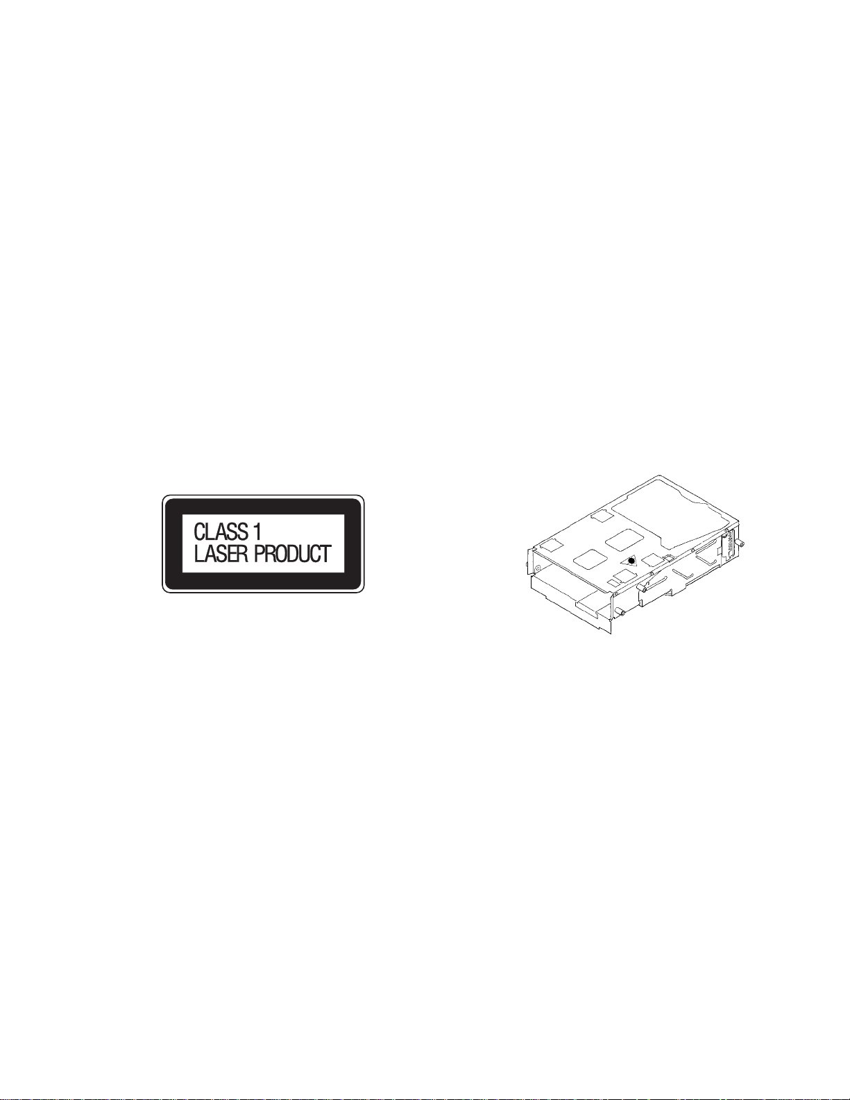
2. A “CLASS 1 LASER PRODUCT” label is affixed to the
rear of the player.
3. The triangular label is attached to the mechanism
unit frame.
1. SAFETY INFORMATION
This service manual is intended for qualified service technicians; it is not meant for the casual do-it-yourselfer.
Qualified technicians have the necessary test equipment and tools, and have been trained to properly and safely repair
complex products such as those covered by this manual.
Improperly performed repairs can adversely affect the safety and reliability of the product and may void the warranty.
If you are not qualified to perform the repair of this product properly and safely; you should not risk trying to do so
and refer the repair to a qualified service technician.
1. Safety Precautions for those who Service this Unit.
• Follow the adjustment steps (see pages 31 through 37)in the service manual when servicing this unit. When checking or adjusting the emitting power of the laser diode exercise caution in order to get safe, reliable results.
Caution:
1. During repair or tests, minimum distance of 13cm from the focus lens must be kept.
2. During repair or tests, do not view laser beam for 10 seconds or longer.
4. Specifications of Laser Diode
Specifications of laser radiation fields to which human access is possible during service.
Wavelength = 785 nanometers
Radiant power = 69.7 microwatts(Through a circular aperture stop having a diameter of 80 millimeters)
0.55 microwatts(Through a circular aperture stop having a diameter of 7 millimeters)
Page 6
4
CDX-M2086ZBM
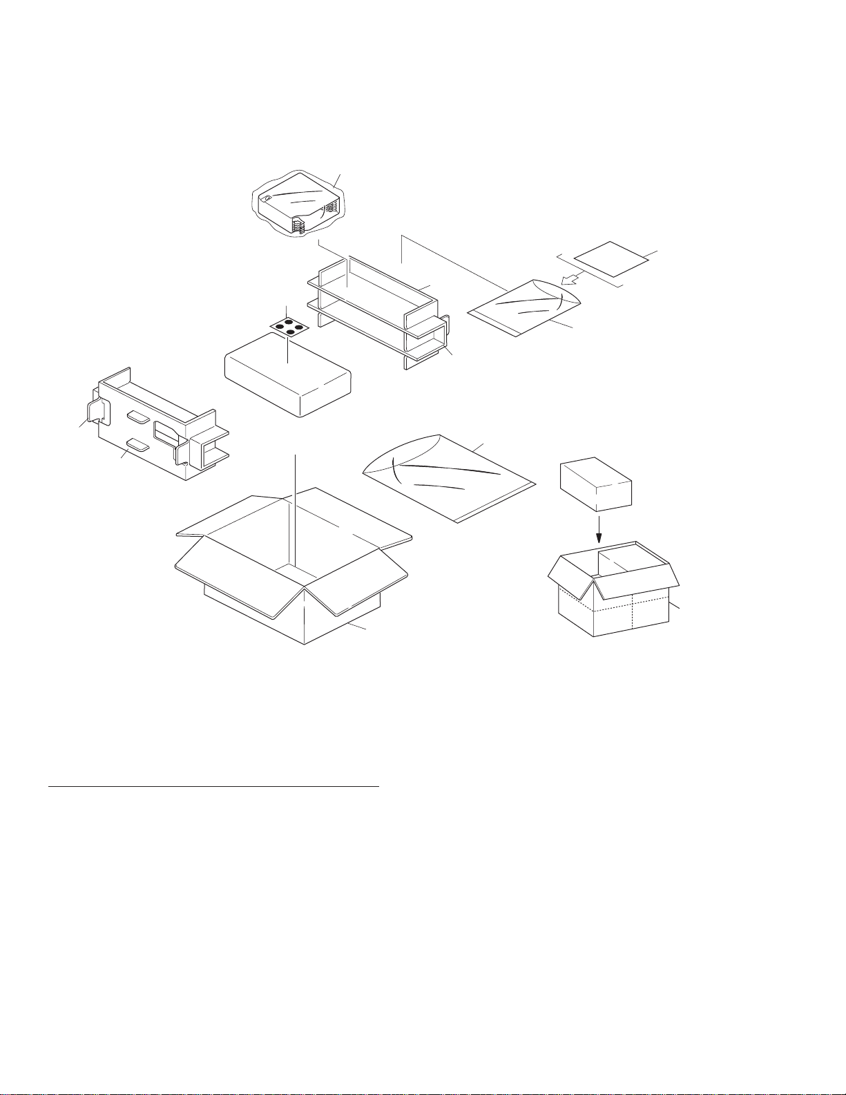
2. EXPLODED VIEWS AND PARTS LIST
2.1 PACKING
7
6
6
7
8
5
3
9
4
1
2
NOTE:
- Parts marked by “*”are generally unavailable because they are not in our Master Spare Parts List.
- Screws adjacent to
∇ mark on the product are used for disassembly.
* 1 Pass Card CRY1122
* 2 Polyethylene Bag E36-615
3 Carton HHG3431
4 Contain Box HHL3431
5 Polyethylene Bag HEG0009
6 Protector HHP1668
7 Protector HHP1669
8 Seal CNM4918
9 Magazine Assy CXB2843
- PACKING SECTION PARTS LIST
Mark No. Description Part No.
Page 7
5
CDX-M2086ZBM
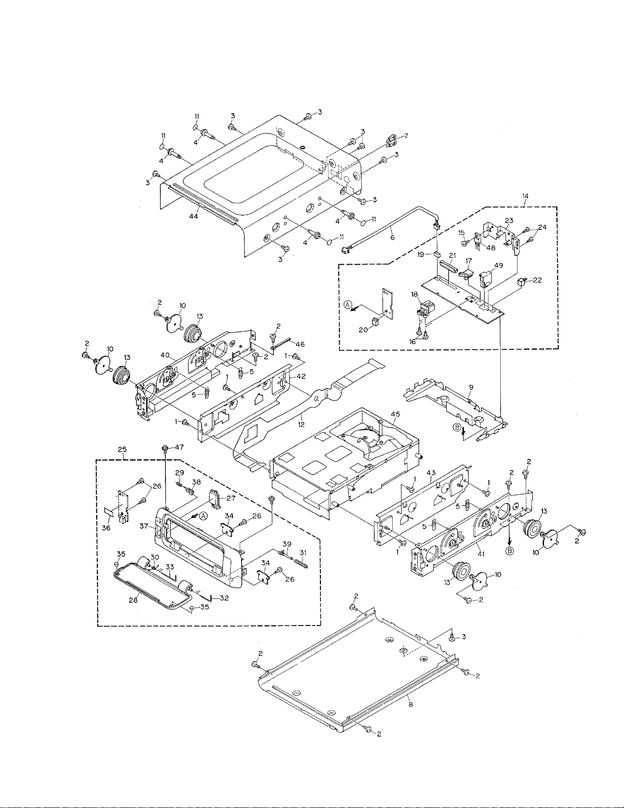
2.2 EXTERIOR
Page 8

6
CDX-M2086ZBM
1 Screw BMZ26P040FMC
2 Screw BMZ30P040FMC
3 Screw BMZ30P040FZK
4 Screw CBA1353
5 Spring CBH2209
6 Cord Assy CDE5367
7 Fuse(5A) CEK1005
8 Lower Case CNB2364
9 Sub Chassis CNC7110
10 Holder CNC7111
11 Seal CNM4918
12 PCB CNP4760
13 Damper CNV5465
14 Extension Unit HWX2132
15 Screw BMZ26P060FMC
16 Screw CBA1407
17 Connector(CN901) CKM1253
18 Connector(CN101) CKM1254
19 Plug(CN702) CKS1036
20 Plug(CN703) CKS1633
21 Connector(CN701) CKS2779
22 Connector(CN201) CKX1012
23 Holder CNC7112
24 Screw PPZ20P060FMC
25 Grille Assy HXB1316
26 Screw BPZ26P080FMC
27 Button CAC5546
28 Door CAT1949
29 Spring CBH1426
30 Spring CBH1983
31 Spring CBH2133
32 Shaft CLA1949
33 Shaft CLA2038
34 Spring Holder CNC3972
35 Cushion CNM5862
36 Sheet CNM6020
37 Grille CNS4895
38 Lever CNV5309
39 Stopper CNV5413
40 Chassis L Assy CXB1618
41 Chassis R Assy CXB1619
42 Frame L Assy CXB1621
43 Frame R Assy CXB1622
44 Upper Case CXB3153
45
CD Mechanism Module(C5) CXK4480
46 Clamper HEF-102
47 Screw IMS30P040FMC
48 Transistor(Q903) 2SB1185
49 Fuse Holder CKR1011
- EXTERIOR SECTION PARTS LIST
Mark No. Description Part No.
Mark No. Description Part No.
Page 9
7
CDX-M2086ZBM
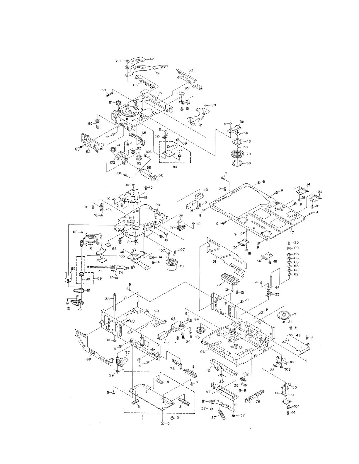
2.3 CD MECHANISM MODULE
Page 10

8
CDX-M2086ZBM
1 CD Core Unit CWX2118
2 Connector(CN701) CKS1968
3 Connector(CN801) CKS3484
4 Connector(CN101) CKS3486
5 Screw IMS26P040FMC
6 Pickup Unit(Service) CXX1235
7 Screw JFZ17P020FNI
8 Volume(VR801) CCW1021
9 Screw(M2x2.5) CBA1037
10 Screw(M2x2.5) CBA1041
11 Screw(M2x2.5) CBA1077
12 Screw(M2x2.5) CBA1085
13 Screw CBA1114
14 Screw CBA1166
15 Screw(M2x2) CBA1176
16 Screw CBA1250
17 Screw(M2x2) CBA1362
18 Screw CBA1387
19 Screw CBA1419
20 Washer CBF1002
21 Washer CBF1038
22 Spring CBH1822
23 Spring CBH1827
24 Spring CBH1830
25 Spring CBH1930
26 Spring CBH1948
27 Spring CBH1972
28 Spring CBH1974
29 Spring CBH2024
30 Spring CBH2091
31 Spring CBL1241
32 Spring CBL1242
33 Spring CBL1295
34 Spring CBL1314
35 Spring CBL1362
36 Spring CBL1388
37 Washer YE20FUC
38 Shaft CLA3087
39 Arm CNC6181
40 Lever CNC6194
41 Lever CNC6534
42 Arm CNC6799
* 43 Holder CNC6819
* 44 Holder CNC6827
45 Plate CNC6847
46 Holder CNC7065
47 Frame CNC7070
48 Cover CNC7074
49 Plate CNC7076
* 50 Bracket CNC7115
51 Lever CNC7715
52 Lever CNC7975
53 Lever CNC8097
54 Spacer CNM4879
* 55 Sheet CNM5020
56 Sheet CNM5118
57 PCB CNP4205
58 PCB CNP4382
59 Ball CNR1189
60 Bearing CNR1423
61 Belt CNT1053
62 Gear CNV4403
63 Gear CNV4404
64 Gear CNV4406
65 Rail(White) CNV4419
66 Rail(Black) CNV4420
67 Lever CNV4422
68 Guide CNV4597
69 Guide CNV4722
70 Holder CNV4761
71 Gear CNV4827
72 Rack CNV4828
73 Cover CNV4924
74 Holder CNV4950
75 Gear CNV4954
76 Guide CNV4982
77 Arm CNV5072
78 Arm CNV5073
79 Clamper CNV5226
80 Gear CNV5305
81 Gear CNV5306
82 Guide CNV5517
83 Speing Switch CSN1033
84 PCB Unit CWX2032
85
Motor Unit(M854)(Carriage) CXB1394
86 Motor Unit(M853)(Tray) CXB1142
87 Motor Unit
(M851)(Spindle) CXB1395
88 Lever Unit CXB1256
89 Screw Unit CXB1270
90 Bearing CNR1423
Mark No. Description Part No. Mark No. Description Part No.
- CD MECHANISM MODULE SECTION PARTS LIST
Page 11

9
CDX-M2086ZBM
91 Arm Unit CXB1476
92 Motor Unit CXB1847
93 Bracket CNC7067
94 Screw JFZ20P025FNI
95 Plate Unit CXB2262
96 Magazine Holder Unit CXB2287
97 Lever Unit CXB2289
98 Frame Unit CXB2290
* 99 Chassis Unit CXB2692
100 Arm Unit CXB2815
101 Damper Unit CXB2816
102 Bracket Unit CXB2962
103 Photo Transistor(Q851) PT4800
104 Switch(S853,S855) CSN1012
105 Chassis Unit CXB3313
106 Screw JFZ20P025FNI
107 Screw JGZ17P022FZK
108 Washer YE15FUC
109 LED(D851) CN504-2
Note: As for brown and orange lead wires, be sure to use the cord kit (CDK1033).
(Shorter or longer wires may lead to malfunctions.)
Mark No. Description Part No.
Page 12
10
CDX-M2086ZBM
2.4 MAGAZINE ASSY
1 Magazine Assy CXB2843
2 Tray CNV5341
- MAGAZINE ASSY SECTION PARTS LIST
Mark No. Description Part No.
Page 13

11
CDX-M2086ZBM
Page 14
12
CDX-M2086ZBM
1
23
4
1234
D
C
B
A
A
B
CD MECHANISM MODULE
3. SCHEMATIC DIAGRAM
3.1 EXTENSION UNIT
Note: When ordering service parts, be sure to refer to “EXPLODED VIEWS AND PARTS LIST” or “ELECTRICAL
PARTS LIST”.
G
Page 15
13
CDX-M2086ZBM
5
6
78
5
6
78
D
C
B
A
A
CTH1129
Page 16
14
CDX-M2086ZBM
1
23
4
1234
D
C
B
A
CCP1338
CCW1021
S851,S852:CSN1033
B
C
B-a
D
E
3.2 CD MECHANISM MODULE(GUIDE PAGE)
B-a B-b
B-a
B-b
B-b
B-a
Large size
SCH diagram
Guide page
Detailed page
F
Page 17

15
CDX-M2086ZBM
5
6
78
5
6
78
D
C
B
A
B-b
B
Page 18

16
CDX-M2086ZBM
1
23
4
1234
D
C
B
A
CCP1338
CCW1021
B-a
B-a
B-b
Page 19

17
CDX-M2086ZBM
5
6
78
5
6
7
8
D
C
B
A
CCP1338
CCW1021
S851,S852:CSN1033
B-a
B-a
B-b
C
D
E
F
Page 20

18
CDX-M2086ZBM
1
23
4
1234
D
C
B
A
B-a
B-a
B-b
Page 21

19
CDX-M2086ZBM
5
6
78
5
6
7
D
C
B
A
B-b
B-a
B-b
8
Page 22

20
CDX-M2086ZBM
- Waveforms
1 RFO 0.5V/div. 0.5µs/div.
Normal mode: play
1 CH1: RFO 1V/div.
2 CH2: MIRR 5V/div.
Test mode: Tracking open
0.5ms/div.
1 CH1: RFO 1V/div.
2 CH2: MIRR 5V/div.
Normal mode: The defect part
passes 800µm
0.5ms/div
3 CH1: FD 0.5V/div.
4 CH2: FOP 2V/div.
Test mode: No disc, Focus close
0.2s/div.
3 CH1: FD 0.5V/div.
5 CH2: FOK 2V/div.
Normal mode: Focus close
0.2s/div.
6 CH1: FEY 0.5V/div.
7 CH2: XSI 2V/div.
Normal mode: Focus close
1ms/div.
REFO
→
8 CH1: TEY 0.5V/div.
9 CH2: TD 0.5V/div.
Test mode: 32 tracks jump (FWD)
0.5ms/div.
8 CH1: TEY 0.5V/div.
9 CH2: TD 0.5V/div.
Test mode: Single jump (FWD)
0.5ms/div.
8 CH1: TEY 0.5V/div.
9 CH2: TD 0.5V/div.
Test mode: 100 tracks jump (FWD)
5ms/div.
6 CH1: FEY 0.1V/div.
3 CH2: FD 0.2V/div.
Normal mode: Play
20ms/div.
3 CH1: FD 0.5V/div.
10 CH2: MDYA 1V/div.
Normal mode: Focus close (12cm)
0.5s/div.
3 CH1: FD 0.5V/div.
10 CH2: MDYA 1V/div.
Normal mode: Focus close (8cm)
0.5s/div.
GND
→
GND
→
REFO
→
REFO
→
REFO
→
REFO
→
GND
→
REFO
→
REFO
→
GND
→
REFO
→
REFO
→
REFO
→
REFO
→
REFO
→
REFO
→
REFO
→
REFO
→
REFO
→
REFO
→
REFO
→
REFO
→
Note:1. The encircled numbers denote measuring pointes in the circuit diagram.
2. Reference voltage
REFO:2.5V
Page 23

21
CDX-M2086ZBM
8 CH1: TEY 0.2V/div.
9 CH2: TD 0.2V/div.
Normal mode: play
8 CH1: TEY 0.5V/div.
11 CH2: SD 0.5V/div.
5ms/div.
10 MDYA 0.5V/div. 0.1s/div.
Normal mode: Play (12cm)
10 MDYA 0.5V/div. 10ms/div.
Long Search (12cm)
12 EFM 1V/div. 5µs/div.
Play
8 CH1: TEY 1V/div.
13 CH2: TEC 1V/div.
Test mode: Focus close
Tracking open
2ms/div.
8 CH1: TEY 0.5V/div.
6 CH2: FEY 0.5V/div.
Normal mode: AGC after focus
0.2s/div.
20ms/div.
14 SCKO 2V/div. 1µs/div.
Play
15 Dout 2V/div. 10µs/div.
Play
16 LRCK 2V/div. 20µs/div.
18 CH1: R OUT 1V/div.
17 CH2: L OUT 1V/div.
Normal mode: Play (1kHz 0dB)
6 CH1: FEY 0.2V/div.
3 CH2: FD 0.5V/div.
Normal mode: During AGC
1ms/div.
0.2ms/div.
REFO
→
REFO
→
REFO
→
REFO
→
REFO
→
REFO
→
GND
→
REFO
→
REFO
→
REFO
→
REFO
→
REFO
→
REFO
→
REFO
→
REFO
→
REFO
→
GND
→
REFO
→
GND
→
REFO
→
GND
→
REFO
→
Page 24

22
CDX-M2086ZBM
8 CH1: TEY 0.2V/div.
9 CH2: TD 0.5V/div.
Normal mode: During AGC
1 CH1: RFO 1V/div.
19 CH2: HOLD 5V/div.
Normal mode: The defect part passes
800µm
1ms/div.
0.5ms/div.
3 CH1: FD 1V/div.
19 CH2: HOLD 5V/div.
Normal mode: The defect part passes
800µm
0.5ms/div.
GND
→
GND
→
REFO
→
REFO
→
REFO
→
Page 25

23
CDX-M2086ZBM
Page 26

24
CDX-M2086ZBM
1
23
4
1234
D
C
B
A
SIDE A
4. PCB CONNECTION DIAGRAM
4.1 EXTENSION PCB
NOTE FOR PCB DIAGRAMS
1. The parts mounted on this PCB
include all necessary parts for
several destination.
For further information for
respective destinations, be sure
to check with the schematic diagram.
Capacitor
Connector
P.C.Board
Chip Part
SIDE A
SIDE B
EXTENSION PCB
A
CN701
B
2. Viewpoint of PCB diagrams
CN703
G
A
Page 27

25
CDX-M2086ZBM
D
C
B
A
1
2
34
1
2
34
A
EXTENSION PCB
A
SIDE B
Page 28

26
CDX-M2086ZBM
1
23
4
1234
D
C
B
A
4.2 CD CORE UNIT
B
SIDE A
CD CORE UNIT
B
PICKUP UNIT
(SERVICE)
CN701
A
C
Page 29

27
CDX-M2086ZBM
D
C
B
A
1
2
34
1
2
34
B
SIDE B
CD CORE UNIT
B
Page 30

28
CDX-M2086ZBM
1
23
4
1234
D
C
B
A
D
PCB UNIT
D
C
C
4.3 PHOTO PCB
4.4 PCB UNIT
PHOTO PCB
C
1
5
10
13
1
2
3
M
SPINDLE
M851
2
1
M
CARRIAGE
M854
GY
YL
BL
BL
Q851
HOME
S853
B
CN801
D
F
E
Page 31

29
CDX-M2086ZBM
D
C
B
A
1
2
34
1
2
34
E
C
F
G
C
A
CN702
MOTOR PCB
E
4.5 MOTOR PCB
SWITCH PCB
F
4.6 SWITCH PCB
BUTTON PCB
G
4.7 BUTTON PCB
Page 32

30
CDX-M2086ZBM
EXTENSION UNIT
Consists of
EXTENSION PCB
BUTTON PCB
Unit Number : HWX2132
Unit Name : Extension Unit
MISCELLANEOUS
IC 101 IC BA3121F
IC 201 IC TC7W04F
IC 401 IC 100.20B
IC 701 IC PD5426A
IC 901 IC PAJ002A
Q 101 Transistor DTC323TK
Q 102 Transistor DTC323TK
Q 103 Transistor IMD2A
Q 105 Transistor DTC323TK
Q 106 Transistor DTC323TK
Q 401 Transistor 2SD1664
Q 701 Transistor DTA124EK
Q 901 Transistor 2SB1260
Q 902 Transistor DTA124EK
Q 903 Transistor 2SB1185
Q 904 Transistor IMX1
D 101 Chip Diode MA151WK
D 102 Diode MA151WA
D 103 Diode MA110
D 104 Diode MA151WA
D 105 Diode MA110
D 401 Diode MA3360(LMH)
D 901 Diode ERA15-02VH
D 902 Diode ERA15-02VH
D 903 Diode ERA15-02VH
D 904 Diode ERA15-02VH
L 401 Inductor LCTB330K2125
L 901 Choke Coil 1.4mH CTH1129
T 201 Transformer CTC1075
TH 701 Thermistor CCX1015
X 701 6.14MHz CSS1336
SW 701 Switch(EJECT) CSG1004
SW 702 Switch(RESET) CSG1035
FU 901 Fuse 5A CEK1005
EF 101 CCG1067
EF 102 CCG1067
RESISTORS
R 101 RS1/10S560J
R 102 RS1/10S560J
R 103 RS1/10S472J
R 104 RS1/10S472J
R 105 RS1/10S362J
R 106 RS1/10S362J
R 107 RS1/16S222J
R 108 RS1/16S222J
R 109 RS1/16S122J
R 110 RS1/16S122J
R 201 RS1/10S101J
R 202 RS1/8S750J
R 401 RS1/10S332J
R 402 RS1/10S102J
R 403 RS1/10S102J
R 404 RS1/10S102J
R 701 RS1/16S433J
R 702 RS1/16S103J
R 704 RS1/10S102J
R 705 RA4C222J
R 706 RA4C104J
R 707 RS1/10S222J
R 708 RS1/10S222J
R 709 RS1/10S102J
R 710 RS1/10S103J
R 711 RS1/10S823J
R 712 RS1/10S222J
R 713 RS1/16S223J
R 714 RS1/10S473J
R 720 RS1/10S562J
R 721 RS1/10S562J
R 777 RS1/10S104J
R 901 RN1/10SE1503D
R 902 RN1/10SE5602D
R 903 RS1/10S103J
R 904 RS1/8S3R9J
R 905 RS1/10S102J
R 906 RS1/10S104J
R 907 RS1/10S104J
R 908 RS1/10S104J
R 909 RS1/10S101J
R 910 RS1/10S223J
R 911 RS1/8S121J
R 912 RS1/8S101J
R 913 RS1/10S122J
R 914 RS1/10S182J
CAPACITORS
C 101 CEJA100M16
C 102 CEJA100M16
C 103 CEJA220M10
C 104 CEJA220M10
C 105 CEJA220M16
C 106 CEJA220M16
C 107 CEJA101M10
C 108 CEAL4R7M16
C 111 CEJA220M10
C 112 CEJA220M10
C 120 CKSQYB104K50
C 201 CKSQYB473K50
C 202 CEJA2R2M50
C 203 CCSQCH680J50
C 204 CKSQYB103K50
5. ELECTRICAL PARTS LIST
NOTE:
- Parts whose parts numbers are omitted are subject to being not supplied.
- The part numbers shown below indicate chip components.
Chip Resistor
RS1/_S___J,RS1/__S___J
Chip Capacitor (except for CQS.....)
CKS....., CCS....., CSZS.....
=====Circuit Symbol and No.===Part Name Part No.
--- ------ ------------------------------------------ -------------------------
A
=====Circuit Symbol and No.===Part Name Part No.
--- ------ ------------------------------------------ -------------------------
G
Page 33

C 205 CEJA470M6R3
C 206 CCSQCH470J50
C 222 CCSQCH102J50
C 402 CKSQYB104K50
C 403 CCSQCH820J50
C 701 CKSRYB103K50
C 702 CKSRYB102K50
C 703 CKSQYB104K50
C 704 CKSQYB104K50
C 705 CKSRYB102K50
C 706 CKSQYB473K50
C 707 CKSQYB473K50
C 708 CCSQCH102J50
C 709 CKSRYB102K50
C 777 CKSQYB104K50
C 901 470µF/16V CCH1183
C 902 470µF/16V CCH1183
C 904 CKSQYB103K50
C 905 CKSQYB104K50
C 906 CSZST330M10
C 907 CKSQYB473K50
C 908 CEJA220M16
C 910 CCSQCH560J50
C 911 CCSQCH560J50
C 913 CCSQCH560J50
C 915 1000µF/16V CCH1149
Unit Number : CWX2118
Unit Name : CD Core Unit
MISCELLANEOUS
IC 101 IC UPC2572GS
IC 201 IC UPD63702AGF
IC 301 IC BA6997FM
IC 302 IC LB1836M
IC 601 IC BA4560F
IC 602 IC BA4560F
IC 604 IC TA78L05F
IC 701 IC PQ05TZ51
Q 101 Transistor 2SD1664
Q 102 Transistor UMD2N
D 701 Diode 1SR154-400
D 702 Diode 1SR154-400
X 201 Crystal Resonator 16.9344MHz CSS1067
VR 802 Semi-fixed 1kΩ(B) CCP1338
RESISTORS
R 101 RS1/8S100J
R 102 RS1/8S120J
R 103 RS1/16S102J
R 104 RS1/16S822J
R 105 RS1/16S682J
R 106 RS1/16S183J
R 107 RS1/16S822J
R 108 RS1/16S333J
R 109 RS1/16S683J
R 110 RS1/16S134J
R 111 RS1/16S273J
R 113 RS1/16S222J
R 114 RS1/16S103J
R 115 RS1/16S103J
R 116 RS1/16S102J
R 117 RS1/16S163J
R 118 RS1/16S163J
R 201 RS1/16S104J
R 202 RS1/16S104J
R 205 RS1/16S102J
R 301 RA4C332J
R 504 RS1/16S102J
R 505 RS1/16S221J
R 506 RA3C221J
R 511 RS1/16S102J
R 601 RS1/16S103J
R 602 RS1/16S103J
R 603 RS1/16S103J
R 604 RS1/16S103J
R 605 RS1/16S912J
R 606 RS1/16S912J
R 607 RS1/16S912J
R 608 RS1/16S912J
R 609 RS1/16S153J
R 610 RS1/16S153J
R 611 RN1/16SE1502D
R 612 RN1/16SE1502D
R 613 RN1/16SK5601D
R 614 RN1/16SK5601D
R 615 RN1/16SK5601D
R 616 RN1/16SK5601D
R 617 RS1/16S562J
R 618 RS1/16S562J
R 619 RS1/16S101J
R 620 RS1/16S101J
R 801 RS1/10S681J
R 804 RS1/16S622J
R 805 RS1/16S562J
CAPACITORS
C 101 CEV101M6R3
C 102 CKSQYB104K16
C 103 CEV470M6R3
C 104 CKSQYB334K16
C 105 CCSRCH330J50
C 106 CKSRYB103K25
C 107 CEV4R7M35
C 108 CKSQYB273K25
C 109 CCSRCH101J50
C 110 CKSQYB104K16
C 111 CKSRYB332K50
C 112 CKSQYB473K25
C 113 CKSRYB103K25
C 114 CKSRYB391K50
C 115 CCSRCH121J50
C 116 CKSRYB682K25
C 117 CKSQYB333K25
C 118 CKSQYB334K16
C 119 CKSQYB334K16
C 120 CKSQYB224K16
C 121 CKSQYB224K16
C 122 CKSQYB104K16
C 123 CKSRYB472K50
C 124 CKSQYB104K16
C 125 CCSRCH6R0D50
C 126 CKSRYB153K25
C 201 CKSQYB334K16
C 202 CKSQYB104K16
C 205 CEV101M6R3
C 206 CKSQYB224K16
C 207 CKSRYB102K50
C 208 CKSQYB224K16
C 209 CCSRCH100D50
C 210 CCSRCH100D50
C 301 CEV101M10
31
CDX-M2086ZBM
=====Circuit Symbol and No.===Part Name Part No.
--- ------ ------------------------------------------ -------------------------
=====Circuit Symbol and No.===Part Name Part No.
--- ------ ------------------------------------------ -------------------------
B
Page 34

32
CDX-M2086ZBM
C 302 CKSQYB224K16
C 601 CCSRCH181J50
C 602 CCSRCH181J50
C 603 CCSRCH820J50
C 604 CCSRCH820J50
C 605 CCSRCH820J50
C 606 CCSRCH820J50
C 607 CKSRYB222K50
C 608 CKSRYB222K50
C 609 CCSRCH331J50
C 610 CCSRCH331J50
C 611 CKSQYB104K16
C 612 CKSQYB104K16
C 613 CKSQYB104K16
C 614 CKSQYB104K16
C 615 CEV101M10
C 701 22µF/6.3V CCH1233
C 702 CKSQYB334K16
C 703 CEV101M6R3
C 801 CKSRYB103K25
C 802 CKSQYB104K16
Unit Number :
Unit Name : Photo PCB
Q 851 Photo-transistor PT4800
S 853 Switch CSN1012
Unit Number : CWX2032
Unit Name : PCB Unit
S 851 Switch(TRP) CSN1033
S 852 Switch(DSP) CSN1033
R 851 RS1/8S473J
R 852 RS1/8S753J
Unit Number :
Unit Name : Motor PCB
M 853 Motor Unit(TRAY) CXB1142
Unit Number :
Unit Name : Switch PCB
S 855 Switch()MAG) CSN1012
Miscellaneous Parts List
D 851 LED CN504-2
M 851 Motor Unit(SPINDLE) CXB1395
M 852 Motor Unit(ELV) CXB1847
M 854 Motor Unit(CARRIAGE) CXB1394
VR 801 10kΩ CCW1021
PU Unit(Service) CXX1235
C
D
E
=====Circuit Symbol and No.===Part Name Part No.
--- ------ ------------------------------------------ -------------------------
F
Page 35

33
CDX-M2086ZBM
6. ADJUSTMENT
6.1 CD ADJUSTMENT
1)Precautions
• This unit uses a single power supply (+5V) for the
regulator. The signal reference potential, therefore, is
connected to REFO(approx. 2.5V) instead of GND.
If REFO and GND are connected to each other by mistake during adjustments,not only will it be impossible
to measure the potential correctly,but the servo will
malfunction and a severe shock will be applied to the
pick-up. To avoid this,take special note of the following.
Do not connect the negative probe of the measuring
equipment to REFO and GND together. It is especially
important not to connect the channel 1 negative
probe of the oscilloscope to REFO with the channel 2
negative probe connected to GND.
Since the frame of the measuring instrument is usually at the same potential as the negative probe,change
the frame of the measuring instrument to floating status.
If by accident REFO comes in contact with
GND,immediately switch the regulator or power OFF.
• Always make sure the regulator is OFF when connect-
ing and disconnecting the various filters and wiring
required for measurements.
• Before proceeding to further adjustments and mea-
surements after switching regulator ON,let the player
run for about one minute to allow the circuits to stabilize.
• Since the protective systems in the unit’s software are
rendered inoperative in test mode,be very careful to
avoid mechanical and /or electrical shocks to the system when making adjustment.
• This unit is adjusted in a combination with the CD
control unit (KEH-P7000, etc.). Each regulator key
should be operated at the unit.
With the KEH-P7000 taken up for reference, a description will be given below concerning how to enter into
the test mode, including key operations. The key in
the adjustment text is also one of the KEH-P7000
keys.
• How to enter into the test mode
Switch ACC,back-up ON while pressing the 4 and 6
keys together.
• Resetting the test mode
Switch ACC,back-up Off.
• Disc detection during loading and eject operations is
performed by means of a photo transistor in this
unit.Consequently,if the inside of the unit is exposed
to a strong light source when the outer casing is
removed for repairs or adjustment,the following malfunctions may occur.
*During PLAY, even if the eject button is pressed,the
disc will not be ejected and the unit will remain in
the PLAY mode.
*The unit will not load a disc.
When the unit malfunctions this way,either re-position the light source,move the unit or cover the
photo transistor.
• When loading and unloading discs during adjustment
procedures,always wait for the disc to be properly
clamped or ejected before pressing another key.
Otherwise, there is a risk of the actuator being
destroyed.
• Turn power off when pressing the button FF or the
button REV key for focus search in the test mode. (Or
else lens may stick and the actuator may be damaged.)
• SINGLE/4TRK/10TRK/32TRK will continue to operate
even after the key is released.Tracking is closed the
moment C-MOVE is released.
• JUMP MODE resets to SINGLE as soon as power is
switched off.
Page 36

34
CDX-M2086ZBM
•Note :
Unlike previous CD mechanism modules the grating angle of the pickup unit cannot be adjusted after the pickup
unit is changed. The pickup unit in the CD mechanism module is adjusted on the production line to match the CD
mechanism module and is thus the best adjusted pickup unit for the CD mechanism module. Changing the pickup
unit is thus best considered as a last resort. However, if the pickup unit must be changed, the grating should be
checked using the procedure below.
•Purpose :
To check that the grating is within an acceptable range.
•Symptoms of Mal-adjustment :
If the grating is off by a large amount symptoms such as being unable to close tracking, being unable to perform
track search operations, or track searching taking a long time, may appear.
•Method :
•Measuring Equipment •Oscilloscope, Two L.P.F.
•Measuring Points •E, F, REFOUT
•Disc •ABEX TCD-784
•Mode •TEST MODE
•Checking Procedure
1. In test mode, load the disc and switch the 5V regulator on.
2. Using the FF and REV buttons, move the pickup unit to the innermost track.
3. Press key 9 to close focus, the display should read "91". Press key 8 to implement the tracking balance adjustment the display should now read "81". Press key 9 4 times. The display will change, returning to "81" on the
fourth press.
4. As shown in the diagram above, monitor the LPF outputs using the oscilloscope and check that the phase difference is within 75° . Refer to the photographs supplied to determine the phase angle.
5. If the phase difference is determined to be greater than 75° try changing the pickup unit to see if there is any
improvement. If, after trying this a number of times, the grating angle does not become less than 75° then the
mechanism should be judged to be at fault.
•Note
Because of eccentricity in the disc and a slight misalignment of the clamping center the grating waveform may be
seen to "wobble" ( the phase difference changes as the disc rotates). The angle specified above indicates the average angle.
•Hint
Reloading the disc changes the clamp position and may decrease the "wobble".
6.2 CHECKING THE GRATING
- Checking the Grating After Changing the Pickup Unit
REFO
E
F
REFO
REFO
E
F
L.P.F.
L.P.F.
CD CORE UNIT
Xch
Ych
Oscilloscope
100kW
100kW
390pF
390pF
Page 37

35
CDX-M2086ZBM
Grating waveform
45
0
75
60
30
90
Ech → Xch 20mV/div, AC
Fch → Ych 20mV/div, AC
Page 38

36
CDX-M2086ZBM
•Note :
Unlike the conventional mechanisms, the new mechanism detects the height of the stage using slide-variable
resistance.
To absorb dislocation of the stage height caused by differences in the mechanism and the CD core unit, adjustment must be made for each CD-mechanism module using a variable resistor.
Normally, readjustment is not needed, as this has been adjusted at the factory. However, adjustment of elevation
is required according to the procedure explained below if an elevation error has occurred or if the CD core unit
has been removed.
•Purpose :
To adjust and confirm whether or not elevation operates correctly.
•Adjustment Method :
•Measuring Equlpment: Millivoltmeter
•Measuring Points : EREF, EPVO
•Setting : Without a magazine in Test mode
With the mechanism placed upside-down (Place the CD mechanism module so that the
CD core unit is above.)
•Confirmation Procedure
1. Enter Test mode, then select Multi-CD player.
2. Press key 7 to enter Mechanism Test mode.
3. Press key 12 twice to specify the amount of movement.
6.3 ADJUSTMENT OF ELEVATION WHEN THE CD CORE UNIT HAS BEEN REMOVED
FOR MAINTENANCE
- Adjustment When Error Code 60 is Displayed Because of Malfunctioning Elevation
TRACK FUNCTION
'"
TRACK FUNCTION
72 00' 00"
EREF
EPVO
mV meter
CD CORE@UNIT
Examples of display
TRACK FUNCTION
72 00' 02"
TRACK FUNCTION
72 00' 01"
The amount of movement
changes each time key 12 is
pressed.
maximum movement
Key 12
during movement
Key 12
minimum movement
TRACK FUNCTION
72 00' 00"
Key 12
Page 39

37
CDX-M2086ZBM
4. Press key 9 to set ELV/TRAY mode to TRAY.
5. Press key FF to release the clamp and return the tray to the magazine.
6. Press key 9 to enter Elevation Move mode.
7. Use key FF/REV to operate elevation and set if to the graduation of the fourth step
(Fig. 1).
8. Make the adjustment.
Use VR802 to adjust the difference in potential between EREF and EPVO to 0 ±20
mV.
9. When adjustment is completed, press key BAND to exit Mechanism Test mode.
10. Confirm operation of the mechanism.
Place the mechanism horizontally (CD core unit below). Take care not to short-circuit the PCB.
11. Confirm the height of the stage. Use the 4 key to select Disc No.4.
Check if the stopper bend of the clamp lever is engaged in the groove of the frame
stopper (Fig. 2-4).
•Note :
The stopper bend will be pressed downward into the groove for final clamping. Confirm the engagement position
of the stopper bend.
•If the stopper bend is engaged in the center and pressed downward, adjustment is completed. Go to step 15.
•If the stopper bend is dislocated, check the amount of dislocation by following steps 12 to 14.
TRACK FUNCTION
72 00' 02"
TRACK FUNCTION
72 00' 02"
TRACK FUNCTION
'"
TRACK FUNCTION
04 00' 00"
Examples of display
TRACK FUNCTION
72 01' 02"
Release the clamp
Page 40

38
CDX-M2086ZBM
12. To see the amount of dislocation, place the mechanism upside-down.
If the stopper bend has been dislocated in the direction of the first
CD, turn VR802 to the left(Fig. 2).
To lower the stage toward the sixth step by 0.1 mm, reduce the voltage of EREF (adjusted in step 8) by 20 mV.
If the stopper bend has been dislocated in the direction of the sixth
CD, turn VR802 to the right(Fig. 4).
To raise the stage toward the first step by 0.1 mm, increase the voltage of EREF (adjusted in step 8) by 20 mV.
13. Place the mechanism horizontal. Go back to step 11 to reconfirm the
stage height.
14. When adjustment of the stage height is completed, proceed as follows:
15. Press the EJECT switch.
16. Once operation of the mechanism has stopped, turn the power OFF.
17. Wait more than one minute after the power is turned off, then turn the power ON and insert a magazine.
18. Check if the mechanism operates correctly with the first and fourth CDs.
19. If the mechanism operates properly, adjustment is completed. If the mechanism operates improperly, make the
adjustment again.
GND
EREF
VR802
mV meter
Page 41

39
CDX-M2086ZBM
E
6
5
4
Adjust to the graduation of the fourth CD.
NG
Fig. 9
Stopper bend of the
clamp lever
Frame stopper
OK
Fig. 10
Engaged in the center and pressed downward.
NG
Fig. 11
Dislocated toward the sixth CD.
Fig. 8
Dislocated toward the first CD.
Fig. 1
Fig. 2
Fig. 3
Fig. 4
Page 42

40
CDX-M2086ZBM
OUT1
-IN1
+IN1
VEE
VCC
OUT2
-IN2
+IN2
-
+
+
-
1
2
BA4560F
7. GENERAL INFORMATION
7.1 IC
100.20B
Page 43

41
CDX-M2086ZBM
- Pin Functions (PD5426A)
Pin No. Pin Name I/O Format Function and Operation
1 VDIN Power supply short sensor input
2–5 NC Not used
6 XA0 O Control signal distinguishing data from microcomputer
7 xsck O NM LSI clock output
8 XSO O NM LSI data output
9 XSI I LSI data input
10 xstb O C CD LSI strobe output
11 xrst O C CD LSI reset output
12–14 NC Not used
15 bsens I Back up power sense input
16 KWAKEUP I BUS data input sense
17–19 NC Not used
20 TXD O C K-BUS data output
21 RXD I K-BUS data input
22 ejsw I Eject signal input
23 mag I Magazine lock switch
24 CNVSS GND
25 reset I Reset input
26 power O C CD +5V control
27 CONT O C Servo driver power supply control
28 XIN I Crystal oscillating element connection pin
29 XOUT O C Crystal oscillating element connection pin
30 VSS GND
31–57 NC Not used
58 MIRR I Mirror detector input
59 LOCK I Spindle lock input (CD)
60 FOK I FOK signal input
61–64 NC Not used
BA6997FM
Page 44

42
CDX-M2086ZBM
Pin No. Pin Name I/O Format Function and Operation
65 I1X3 O C Motor driver control output
66 I2 O C Motor driver control output
67 I4 O C Motor driver control output
68 CDMUTE O C CD mute output
69 adena O C AVREF enable output
70 testin I Test program mode input
71 VCC 5V
72 VREF I A/D converter reference voltage input
73 AVSS I A/D GND
74,75 NC Not used
76 disk Disc detector input
77 ELVPVO I Voltage input from ELV position sense
78 ELVREF I Voltage input from ELV
79 MSW I Disc sense timing input and tray position input
80 TEMP Temperature detector
*PD5426A
80
1
20
21 40
41
60
61
Format Meaning
C C MOS
NM Middle N channel open drain
IC's marked by* are MOS type.
Be careful in handling them because they are very
liable to be damaged by electrostatic induction.
Page 45

43
CDX-M2086ZBM
7.2 DIAGNOSIS
7.2.1 DISASSEMBLY
- Removing the Upper Case
1.Remove the eight screws and then remove the upper case.
- Removing the Extension PCB
1.Remove the two screws.
2.Stretch the claw indicated by arrow and then remove
the extension PCB.
Note : Before disassembling the CD mech module, turn the spring holder so that the spring is positioned
horizontally. After reassembling, return the spring to the vertical position.
EXTENSION PCB
Page 46

44
CDX-M2086ZBM
7.2.2 TEST MODE
Before entering the test modes, remove the EXTENSION PCB and connect the jig (GGF1342) as shown
below.
GGF1342
Page 47

45
CDX-M2086ZBM
- Flow Chart
<Power OFF>
46
ACC, Back-up ON
<CD multi player selected>
BAND
<Power OFF>
TRACK FUNCTION
<Focus closed>
00"00'
Display
BAND
SOURCE
<Power ON>
<Tracking
closed >
AGC YES
TRACK FUNCTION
00"00'
Display
BAND
TRACK
Display Display
FUNCTION
00"00'00
912
<Focus mode
select>
Display
TRACK
FUNCTION
*1
91"91'91
8
7
TRACK
TRACK
Display
<Tracking
closed >
FUNCTION
81"81'81
12
AGC NO
FUNCTION
56"02'1
Display
example
12
<New test mode in>
7
<Tracking closed >
TRACK FUNCTION
FF
<Carriage shifted
outwards while
this key is pressed>
9 FF REV
*2
<Auto adjustment
display>
<Carriage shifted
outwards while
this key is pressed>
During regulator off, press the 12
key and the system will be put into
the new test mode.
00"00'
REV
<Carriage shifted
inwards while
this key is pressed>
<Carriage shifted
inwards while
this key is pressed>
BAND
<Power OFF>
BAND
<Power OFF>
<Carriage MOVE
or T.jump>
FF REV
*3
<Carriage MOVE
or T.jump>
8
<Tracking open >
TRACK
*3 *4
<T.jump mode
change>
FUNCTION
12
00"00'72
< Mechanism test mode in >
912FF7REV BAND
*6 *9*8*7
<ELV,TRAY select>
*1 Normal focus close S curve check Focus EQ check
00"00'00 01"01'01 02"02'02
*2 Normal display Focus cancel Tracking balance
*3 100 TRK jump and carriage MOVE continue only while the keys are released
*4 SINGLE
81 8685848382
4TRK 10TRK 32TRK 100TRK C.MOVE
Display
*5 Normal display Focus gain Tracking gain Focus bias
Display
<Operation mode
select >
Display
<Shift > <Shift >
Tracking offset
(Close spindle-rough)
7
<AGC display
select>
*5
98
<AGC >
TRACK FUNCTION
Display
TRACK FUNCTION
00"00'
Display
<Mechanism test
mode out >
*6 ELV motor select
0X"00'72
8ms pulse drive
*7
00"00'72 01"00'72 02"00'72
48ms pulse drive
00"10'72
ELV select : ELV dowm (Disc 1
*8
TRAY select : TRAY out
*9 ELV select : ELV up (Disc 6
TRAY select : TRAY in
TRAY motor select
Display
24ms pulse drive DC drive
Display
100ms pulse drive DC drive
Display
<Tracking open>
0X"10'72
01"10'72 02"10'72
¤
6)
¤
1)
00"00'
Page 48

46
CDX-M2086ZBM
- New Test Mode(aging operation and setup analysis)
The single CD player plays in normal mode. After being set up, it will display FOK (focus), LOCK (spindle), subcode,
sound skip, protection against a mechanical error or the like, occurrence of an error, cause and time of an expiry, if
any, (and disc number)
During the setup, the CD software operation status (internal RAM and C-point)is displayed.
(1) How to enter NEW TEST Mode
See the test mode flow chart Page 43.
(2) Relations of keys between TEST and NEW TEST Modes
Keys Test Mode New Test Mode
Regulator OFF Regulator ON PLAY in progress Error Occurred,
Protection Activated
BAND Regulator ON Regulator OFF Time of occurrence/
cause of error select
FF FWD-Kick FF/TRACK+
REV REV-Kick REV/TRACK-
7 Tracking close SCAN
8 Tracking open MODE
9 Focus close
12 To New Test Jump Mode AUTO/MANU TRACK No./
Mode Select time of occurrence select
Operations,such as EJECT, CD ON/OFF, etc. are performed normally
(3) Error Cause (Error Number) Code
Error Code Classification Mode Description Cause/Detail
40 ELECTRIC PLAY FOK=L Put out of focus
100ms Scratch,
41 ELECTRIC PLAY LOCK=L Spindle unlock Stain,
100ms Vibration,
42 ELECTRIC PLAY Subcode Failed to read subcode Servo defect,
unacceptable 500ms etc...
43 ELECTRIC PLAY Sound skipped Last address memory
operated
(4) Indicating an Operation Status During Setup
Status No. Description Protection operation
01 Carriage home mode started None
02 Carriage moving inwards 10-second time out, Home switch failed
03 Carriage moving outwards 10-second time out, Home switch failed
05 Carriage moving outwards None
11 Setup started None
12 Spindle turn/Focus search started None
13 Waiting for focus closure (XSI=L) Failure to close focus
10,14 Waiting for focus closure (FOK=H) Failure to close focus
15, 16, 17 Focus closed, Tracking open Focus disrupted
18 During focus AGC Focus disrupted
19 During tracking AGC Disrupted focus
20 Waiting for MIRR, LOCK or subcode read Focus disrupted, MIRR NG, Failure to lock,
Carriage closed, SPINDLE=ADAPTIVE failed to read subcode
Page 49

47
CDX-M2086ZBM
(5) Example of Display.
•SET UP in progress
8 digits display LCD
•Operation (PLAY, SEARCH, etc.) in progress perfectly
identical with that in the normal mode.
•Protection/Error upon occurrence(8 digits display LCD)
(a) Error number indicated
Select the display with the
BAND key.
(b) Track number and
absolute time indicated
ERROR–xx
TNo.10Min40Sec
05
- Error Number Indication
If the CD should fail to operate or if an error has taken place during operation the player will enter into the error
mode, and the cause of the error will be numerically indicated.
This is aimed at assisting in analysis or repair.
(1) Basic Means of Display
•Examples of Display ERROR-xx
(2) Error Codes
Error Classification Description Cause/Detail
Code
10 ELECTRIC Carriage home failure Carriage doesn't move to or from the innermost position
→Home switch failed and/or carriage immobile
11 ELECTRIC Focus failure Focus failed
→Defects, disc upside-down, severe vibration
12 ELECTRIC SETUP failure Spindle failed to lock or subcode unreadable
Subcode failure →Spindle defective, defect, severe vibration
14 ELECTRIC Mirror failure Unrecorded CD-R
The disc is upside-down, defects, vibration
17 ELECTRIC Set up failure AGC protect failed
→Defects, disc upside-down, severe vibration
19 ELECTRIC Set up failure Tracking error waveform is too unbalanced (>50%) or
level is too small
→The pickup unit or tracking error circuitry is N.G.
30 ELECTRIC Search time out Failed to reach target address
→Carriage/tracking defective and/or defects
A0 SYSTEM Power failure Power overvoltage or short circuit detected
→Switching transistor defective and/or power abnormal
A1 SYSTEM Mechanism power Mechanism elevation reference voltage is out of
failure prescription
→EREF adjustment VR and/or power abnormal
50 MECHANISM An error upon ejection MAG switch release time has time out
Elevation time out when eject
60 MECHANISM An error while putting in Tray in / out time has time out
and out the tray Tray is caught when put in
70 MECHANISM An error upon elevation Elevation time has time out
80 MECHANISM An error with an empty No disc is available
magazine inserted
* Setup means a series of operations after focusing up to sound output.
TNo.11Min11Sec
11
Page 50

48
CDX-M2086ZBM
7.2.3 CONNECTOR FUNCTION DESCRIPTION
KBUS
BATT
GND
Audio Right+
Audio Left+
Audio Right-
Audio Left-
Ground
Ground
Page 51

49
CDX-M2086ZBM
7.3 BLOCK DIAGRAM
A
B
C
D
E
F
G
Page 52

CDX-M2086ZBM
8. OPERATIONS AND SPECIFICATIONS
8.1 OPERATION
8.2 SPECIFICATIONS
RESET BUTTON
EJECT
General
System . . . . . . . . . . . . . . . . . . . . . . . . . . . . . . . . . . .Compact disc audio system
Usable discs . . . . . . . . . . . . . . . . . . . . . . . . . . . . . . . . . . . . . . . . . . .Compact Disc
Signal format . . . . . . . . . . . . . . . . . . . . . . . . . . . . .Sampling frequency:44.1 kHz
Number of quantization bits: 16; linear
Power source . . . . . . . . . . . . . . . . . . . . . . . . . . . . . . . . . . . . . . . . . . . . .14.0 V DC
10.8 16.0 V
Max. current consumption . . . . . . . . . . . . . . . . . . . . . . . . . . . . . . . . . . . . . .3.0 A
Weight . . . . . . . . . . . . . . . . . . . . . . . . . . . . . . . . . . . . . . . . . . . . . . . . . . . . . .2.8 kg
Dimensions . . . . . . . . . . . . . . . . . . . . . . . . . . . . . . . . . .200(W)x77.5(H)x299.6(D)
Audio
Frequency characteristics . . . . . . . . . . . . . . . . . . . . . . . . . . . . .20 20.000(±1dB)
Signal-to-noise ratio . . . . . . . . . . . . . . . . . .85dB or more(1kHz)(20kLPF,A-Filter)
Distortion . . . . . . . . . . . . . . . . . . . . . . . . . . . . . . . . .0.08% or less(1kHz)(20kLPF)
Dynamic range . . . . . . . . . . . . . . . . . . . . . . . . . . . . . . . . . . . . . . . . .85dB or more
Output level . . . . . . . . . . . . . . . . . . . . . . . . . . . . . . . . .500mV±100mV(1kHz,0dB)
Number of channels . . . . . . . . . . . . . . . . . . . . . . . . . . . . . . . . . . . . . . . .2(stereo)
Note:
Specifications and design are subject to possible modification without prior
notice due to improvements.
 Loading...