

Page 1
PIONEER ELECTRONIC CORPORATION 4-1, Meguro 1-Chome, Meguro-ku, Tokyo 153-8654, Japan
PIONEER ELECTRONICS SERVICE INC. P.O.Box 1760, Long Beach, CA 90801-1760 U.S.A.
PIONEER ELECTRONIC [EUROPE] N.V. Haven 1087 Keetberglaan 1, 9120 Melsele, Belgium
PIONEER ELECTRONICS ASIACENTRE PTE.LTD. 501 Orchard Road, #10-00, Wheelock Place, Singapore 238880
C PIONEER ELECTRONIC CORPORATION 1998
K-ZED. JAN.1998 Printed in Japan
ORDER NO.
CRT2163
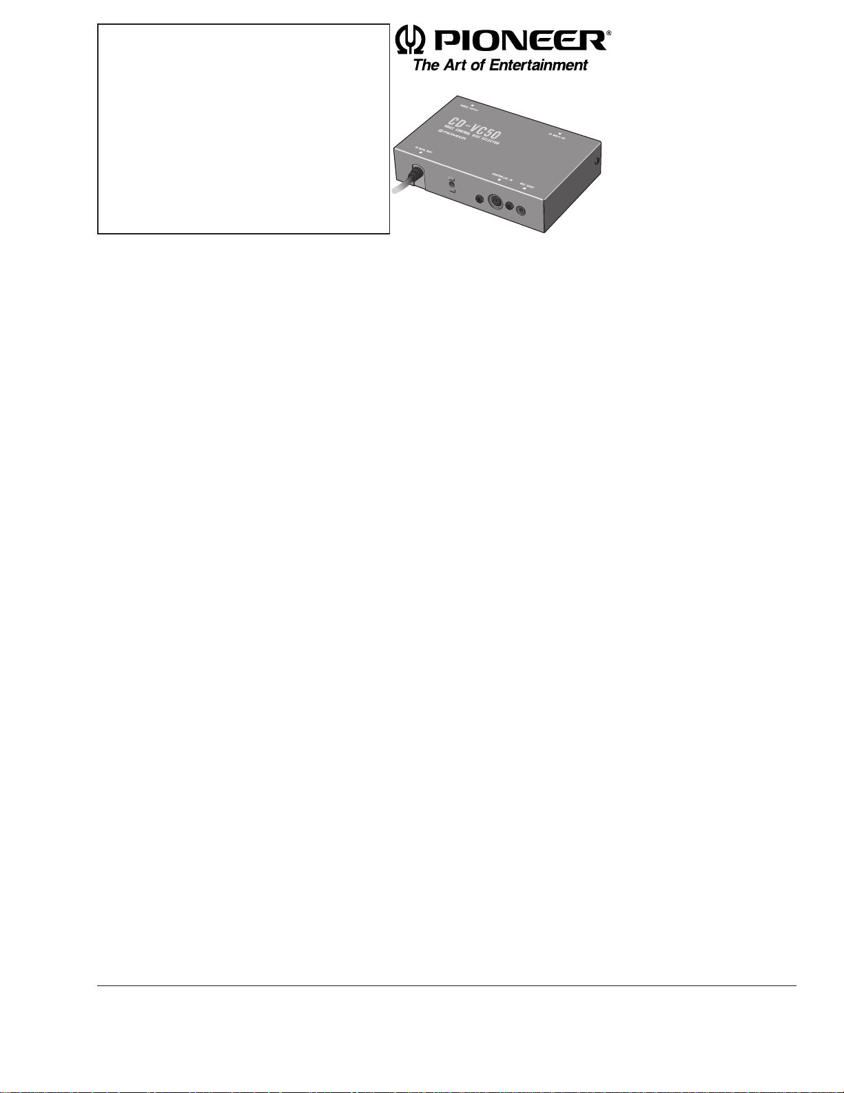
VOICE CONTROL DISC SELECTOR
Se
r
vic
e
M
a
nu
a
l
CD-VC50-02 E
CONTENTS
1. SAFETY INFORMATION ............................................2
2. EXPLODED VIEWS AND PARTS LIST.......................3
3. SCHEMATIC DIAGRAM .............................................6
4. PCB CONNECTION DIAGRAM ..................................8
5. ELECTRICAL PARTS LIST ........................................10
6. ADJUSTMENT..........................................................12
7. GENERAL INFORMATION .......................................12
7.1 IC .........................................................................12
7.2 DIAGNOSIS ........................................................15
7.2.1 TEST MODE..............................................15
7.2.2 DISASSEMBLY .........................................16
7.3 BLOCK DIAGRAM ..............................................17
8. OPERATIONS AND SPECIFICATIONS.....................18
Page 2

2
CD-VC50-02
1. SAFETY INFORMATION
CAUTION
This service manual is intended for qualified service technicians; it is not meant for the casual do-it-yourselfer.
Qualified technicians have the necessary test equipment and tools, and have been trained to properly and safely repair
complex products such as those covered by this manual.
Improperly performed repairs can adversely affect the safety and reliability of the product and may void the warranty.
If you are not qualified to perform the repair of this product properly and safely; you should not risk trying to do so
and refer the repair to a qualified service technician.
W
ARNING
Lead in solder used in this product is listed by the California Health and Welfare agency as a known reproductive
toxicant which may cause birth defects or other reproductive harm (California Health and Safety Code, Section
25249.5). When servicing or handling circuit boards and other components which contain lead in solder, avoid
unprotected skin contact with the solder. Also, when soldering do not inhale any smoke or fumes produced.
Fig. 1
Page 3
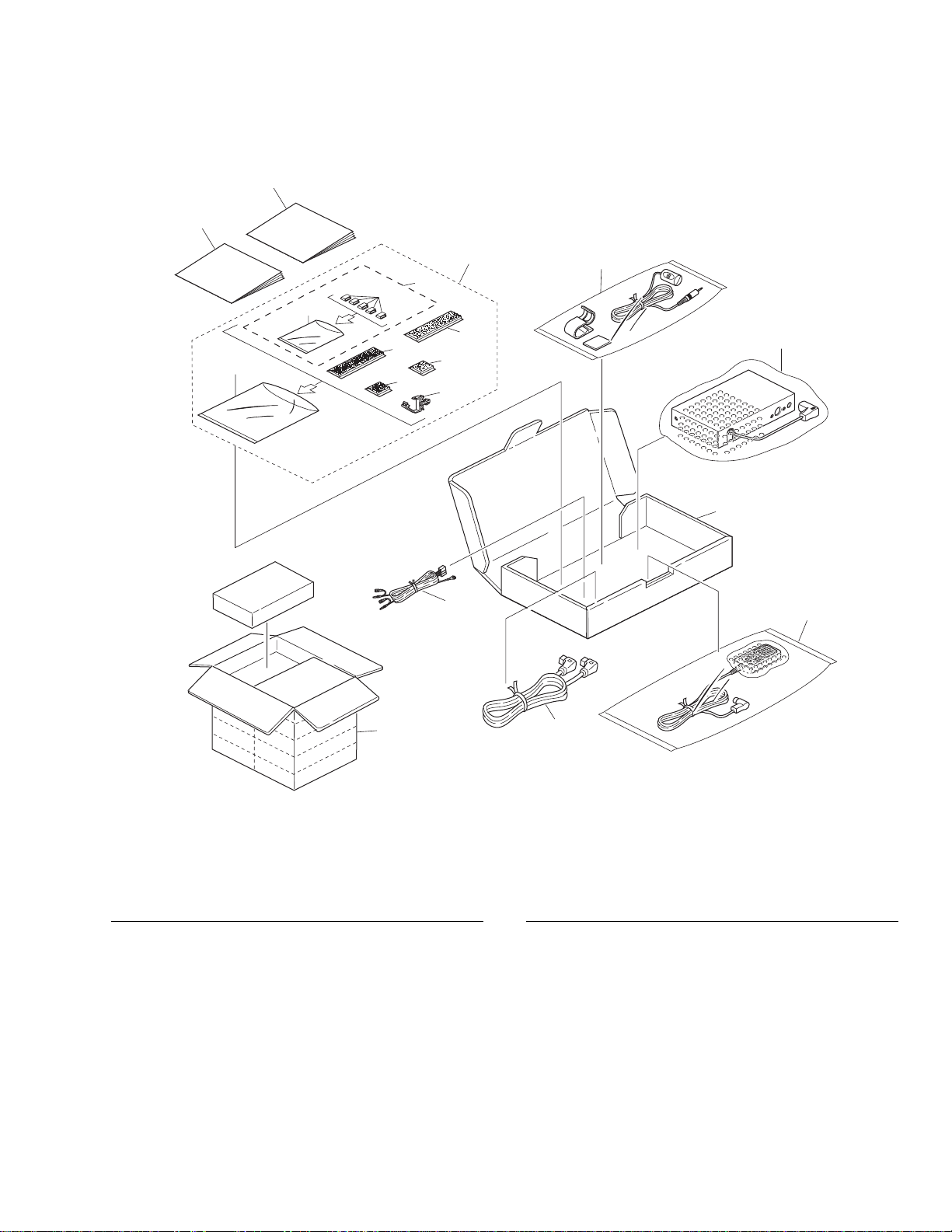
- PACKING SECTION PARTS LIST
Mark No. Description Part No.
Mark No. Description Part No.
3
CD-VC50-02
1 Carton CHG3112
2 Contain Box CHL3112
3 Owner’s Manual CRD2188
(English, French, Spanish,
German, Italian)
* 4 Accessory Assy CEA2315
5 Cord Clamper Assy CEA2072
6 Cord Clamper CNV2581
* 7 Polyethylene Bag E36-615
* 8 Polyethylene Bag CEG-238
9 Fastener(rough)(S) CNM3709
10 Fastener(soft)(S) CNM3710
11 Fastener(rough)(L) CNM3728
12 Fastener(soft)(L) CNM3729
13 Clamper CNV3751
14 Air Cushioned Bag CEG1089
15 Microphone Assy CPM1017
16 Controller Assy CXB2569
17 Cord(Power supply) CDE5122
18 Cord Assy(IP-BUS) CDE5056
19 Owner’s Manual CRB1401
(Dutch)
2. EXPLODED VIEWS AND PARTS LIST
2.1 PACKING
NOTE:
- Parts marked by “*”are generally unavailable because they are not in our Master Spare Parts List.
- Screws adjacent to ∇ mark on the product are used for disassembly.
14
16
17
18
6
4
8
7
13
10
11
12
9
5
2
1
15
3
19
Page 4
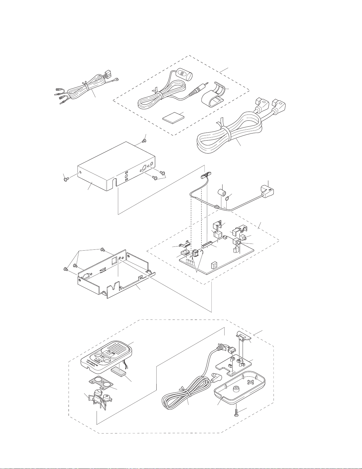
4
CD-VC50-02
2.2 EXTERIOR
Fig. 2
1
17
19
21
20
1
18
1
16
14
13
11
15
3
2
9
8
1
12
7
10
6
5
4
31
22
25
26
30
24
23
27
28
29
Page 5

5
CD-VC50-02
1 Screw BSZ30P060FZK
2 Case CNB2122
3 Processor Unit CWX2242
4 Chassis CNA1839
5 Clamper CEF1005
6 Plug(CN701) CKM1131
7 Plug(CN302) CKS1044
8 Jack(CN101) CKS2310
9 Connector(CN301) CKS2486
10 Connector(CN901) CKS3195
11 Holder CNC6686
12 Bracket CZN6159
13 Bracket CZN6234
14 Cord Assy CDE5358
* 15 Lock Tie CNV-754
* 16 Filter CTX1060
17 Cord CDE5122
18 Cord Assy CDE5056
19 Microphone Assy CPM1017
20 Cushion MEH1007
21 Clip Stand MNK1221
22 Grille Assy TXK1475
23 Cover TED1364
24 Button TMA1030
25 Spacer TMA1028
26 PCB Unit TWX1021
27 Cord Assy TDC2159
28 Case TMB1044
29 Screw PPZ26P080FZK
30 Cushion TED1366
31 Controller Assy CXB2569
- EXTERIOR SECTION PARTS LIST
Mark No. Description Part No.
Mark No. Description Part No.
Page 6
6
CD-VC50-02
A
1
234
B
C
D
12
34
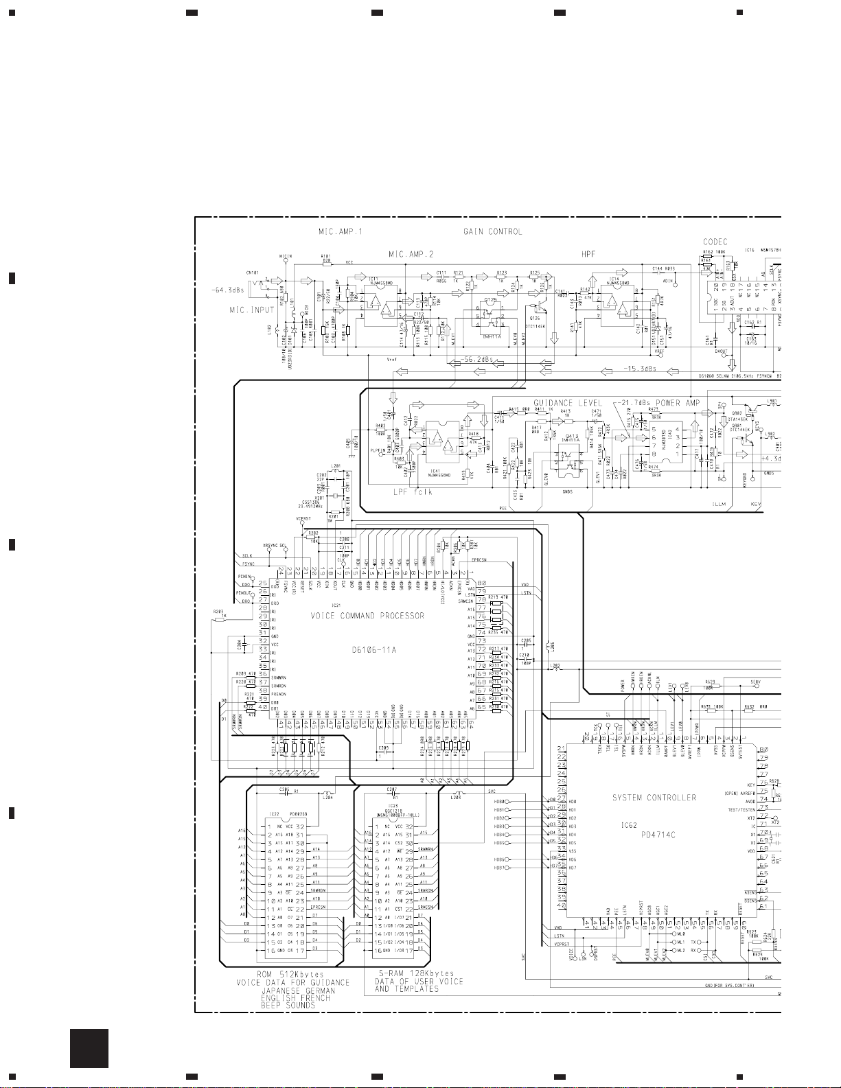
3. SCHEMATIC DIAGRAM
3.1 OVERALL CONNECTION DIAGRAM
Note: When ordering service parts, be sure to refer to “EXPLODED VIEWS AND PARTS LIST” or “ELECTRICAL PARTS
LIST”.
A
HPF
REF.VOLT
Page 7

7
CD-VC50-02
5
6
7
8
A
B
C
D
5
6
7
8
Fig. 3
A
Page 8

8
CD-VC50-02
A
1
234
B
C
D
12
34
4. PCB CONNECTION DIAGRAM
4.1 MAIN UNIT
A
Capacitor
Connector
P.C.Board
Chip Part
SIDE A
SIDE B
NOTE FOR PCB DIAGRAMS
1. The parts mounted on this PCB
include all necessary parts for
several destination.
For further information for
respective destinations, be sure
to check with the schematic
diagram.
2. Viewpoint of PCB diagrams
RESET
SERVICE
A
PROCESSOR UNIT
SIDE A
Fig. 4
CONTROLLER ASSY
CORD ASSY(POWER SUPPLY)
CORD ASSY(IP BUS)
Page 9

9
CD-VC50-02
5
6
7
8
A
B
C
D
5
6
7
8
A
SIDE B
Fig. 5
A
PROCESSOR UNIT
Page 10

10
CD-VC50-02
Unit Number : CWX2242
Unit Name : Processor Unit
MISCELLANEOUS
IC 11 IC NJM4558MD
IC 14 IC NJM4558MD
IC 16 IC MSM7578HMS
IC 21 IC D6106-11A
IC 22 IC PD8026B
IC 23 IC (M5M51008BFP-10LL) GGC1218
IC 41 IC NJM4558MD
IC 42 IC NJM2073D
IC 61 IC HA12187FP
IC 62 IC PD4714C
IC 71 IC NJM7805FA
IC 73 IC NJM78L05A
IC 81 IC NJM78M06FA
IC 82 IC S-80730ANDT
Q 125 Transistor IMH11A
Q 126 Transistor DTC114EK
Q 413 Transistor IMH11A
Q 711 Transistor 2SB1243
Q 712 Transistor 2SD1859
Q 713 Transistor DTC143EK
Q 731 Transistor 2SB1243
Q 732 Transistor DTC143EK
Q 831 Transistor 2SC2412K
Q 832 Transistor 2SC2412K
Q 901 Transistor DTC144EK
Q 902 Transistor DTA143EK
D 101 Diode UDZ3R3(B)
D 151 Diode UDZ4R7(B)
D 701 Diode ERA15-02VH
D 702 Diode ERA15-02VH
D 711 Diode UDZ9R1(B)
D 811 Diode 1SS356
D 812 Diode 1SS356
D 821 Diode 1SS356
D 831 Diode HZS7L(C2)
D 832 Diode RD2R2ES(B1)
L 101 Inductor LCTBR47K2125
L 102 Ferri-Inductor LAU101K
L 201 Inductor LCTB1R8K2125
L 202 Inductor LAU3R3K
L 203 Inductor LCTBR47K2125
L 204 Inductor LCTBR47K2125
L 205 Ferri-Inductor LAU101K
L 601 Inductor LCTBR47K2125
L 602 Inductor LCTBR47K2125
L 701 Choke Coil 1.4mH CTH1129
L 901 Inductor LCTBR47K2125
L 902 Inductor LCTBR47K2125
X 201 Resonator 29.4912MHz CSS1386
X 621 Resonator 6.29MHz CSS1307
S 801 Switch CSG1059
RESISTORS
R 101 RS1/10S821J
R 102 RS1/10S681J
R 103 RS1/10S153J
R 104 RS1/10S103J
R 105 RS1/10S102J
R 112 RS1/10S103J
R 113 RS1/10S104J
R 114 RS1/10S103J
R 115 RS1/10S101J
R 121 RS1/10S102J
R 122 RS1/10S102J
R 123 RS1/10S102J
R 124 RS1/10S102J
R 125 RS1/10S102J
R 126 RS1/10S102J
R 141 RS1/10S473J
R 142 RS1/10S473J
R 151 RS1/10S472J
R 161 RS1/10S473J
R 162 RS1/10S104J
R 163 RS1/10S103J
R 201 RS1/10S105J
R 202 RS1/10S103J
R 203 RS1/10S102J
R 204 RS1/10S103J
R 206 RS1/10S103J
R 207 RS1/10S103J
R 208 RS1/10S681J
R 209 RS1/10S471J
R 211 RA4C471J
R 212 RS1/10S471J
R 215 RS1/10S471J
R 216 RS1/10S471J
R 217 RS1/16S471J
R 219 RA3C471J
R 220 RS1/10S471J
R 221 RS1/10S471J
R 222 RS1/10S471J
R 223 RS1/10S471J
R 224 RS1/16S0R0J
R 225 RS1/16S0R0J
R 226 RS1/10S471J
R 227 RS1/10S471J
R 228 RS1/10S471J
R 229 RS1/10S471J
R 230 RS1/10S471J
R 231 RS1/10S471J
R 232 RS1/10S471J
R 233 RS1/16S471J
R 234 RS1/10S471J
=====Circuit Symbol and No.===Part Name Part No.
--- ------ ------------------------------------------ -------------------------
=====Circuit Symbol and No.===Part Name Part No.
--- ------ ------------------------------------------ -------------------------
5. ELECTRICAL PARTS LIST
NOTE:
- Parts whose parts numbers are omitted are subject to being not supplied.
- The part numbers shown below indicate chip components.
Chip Resistor
RS1/_S___J,RS1/__S___J
Chip Capacitor (except for CQS.....)
CKS....., CCS....., CSZS.....
A
Page 11

11
CD-VC50-02
R 235 RS1/10S471J
R 401 RS1/10S103J
R 402 RS1/10S104J
R 403 RS1/10S103J
R 411 RS1/10S102J
R 412 RS1/10S152J
R 413 RS1/10S102J
R 414 RS1/10S152J
R 415 RS1/10S0R0J
R 417 RS1/10S0R0J
R 418 RS1/10S473J
R 419 RS1/10S473J
R 421 RS1/10S104J
R 422 RS1/10S103J
R 423 RS1/10S103J
R 471 RS1/10S562J
R 472 RS1/10S473J
R 473 RS1/10S332J
R 474 RS1/10S332J
R 475 RS1/10S271J
R 476 RS1/10S100J
R 601 RS1/10S101J
R 602 RS1/10S101J
R 603 RS1/10S473J
R 604 RS1/10S473J
R 623 RS1/10S104J
R 624 RS1/10S222J
R 625 RS1/10S104J
R 626 RS1/10S222J
R 627 RS1/10S103J
R 628 RS1/10S101J
R 629 RS1/10S104J
R 630 RS1/10S104J
R 631 RS1/10S104J
R 711 RS1/10S103J
R 712 RS1/10S222J
R 713 RS1/10S472J
R 731 RS1/10S103J
R 732 RS1/10S222J
R 801 RS1/10S104J
R 803 RS1/10S102J
R 806 RS1/10S102J
R 807 RS1/10S101J
R 808 RS1/10S104J
R 811 RS1/10S101J
R 823 RS1/10S223J
R 824 RS1/10S223J
R 825 RS1/10S473J
R 826 RS1/10S473J
CAPACITORS
C 101 CEJAR22M50
C 102 CEAL101M10
C 103 CKSQYB472K50
C 104 CCSQCH151J50
C 105 CKSQYB102K50
C 106 CCSQCH101J50
C 111 CKSQYB563K16
C 112 CEJAR22M50
C 113 CKSQYB471K50
C 114 CEAL470M16
C 141 CKSQYB223K50
C 142 CKSQYB103K50
C 143 CKSQYB123K50
C 144 CKSQYB333K50
C 151 CEAL470M16
C 161 CKSQYB104K50
C 162 CKSQYB104K50
C 163 CEJA100M16
C 201 CCSQCH100J50
C 202 CCSQCH220J50
C 203 CKSQYB102K50
C 204 CKSYB105K16
C 205 CKSYB105K16
C 206 CKSQYB104K50
C 207 CKSQYB104K50
C 208 CKSYB105K16
C 209 CKSYB105K16
C 210 CCSQCH101J50
C 211 CCSQCH101J50
C 301 CKSQYB104K50
C 302 CKSQYB102K50
C 303 CKSQYB102K50
C 401 CEJA1R0M50
C 402 CKSQYB332K50
C 403 CKSQYB682K50
C 404 CKSQYB103K50
C 405 CEAL101M10
C 411 CEJA1R0M50
C 412 CKSQYB223K50
C 413 CKSQYB123K50
C 422 CKSQYB103K50
C 423 CKSQYB103K50
C 471 CEJA1R0M50
C 472 CKSQYB224K16
C 473 CKSQYB223K50
C 474 CKSQYB223K50
C 475 CEJA1R0M50
C 476 CEJA1R0M50
C 477 CEAL101M10
C 478 CKSQYB104K50
C 601 CKSQYB471K50
C 602 CKSQYB471K50
C 603 CKSQYB102K50
C 604 CKSQYB102K50
C 605 CKSQYB104K50
C 621 CKSQYB104K50
C 701 470µF/16V CCH1183
C 702 CKSQYB102K50
C 704 470µF/16V CCH1183
C 705 470µF/16V CCH1183
C 706 EMI Filter CCG1006
C 707 CKSQYB102K50
C 711 CEAS331M16
C 712 CEAL470M16
C 713 CEAL101M10
C 714 CKSQYB104K50
C 715 CEJAR68M50
C 716 CKSQYB104K50
C 731 CKSQYB104K50
C 732 CEJAR68M50
C 733 CKSQYB104K50
C 801 CKSQYB104K50
C 803 CEJA1R0M50
C 811 CEJA221M6R3
C 812 0.1F/5.5V CCL1023
C 821 CSZA220M16
C 831 CKSQYB104K50
C 832 CKSQYB104K50
C 833 CEJA221M6R3
C 834 CEJAR68M50
C 901 CCSQCH101J50
C 903 CKSQYB102K50
=====Circuit Symbol and No.===Part Name Part No.
--- ------ ------------------------------------------ -------------------------
=====Circuit Symbol and No.===Part Name Part No.
--- ------ ------------------------------------------ -------------------------
Page 12

12
CD-VC50-02
7. GENERAL INFORMATION
7.1 IC
6. ADJUSTMENT
There is no information to be shown in this chapter.
- Pin Functions(PD4714C)
Pin No. Pin Name I/O Format Function and Operation
1 SVTEST I Service testmode input
2 GSENS I Select input for the distination
3 VCPPW O C Power supply for D6106,ROM
4 AVSS I GND
5 NC Not used
6 IPPW O C Power supply control output for IP BUS driver
7 AVREF1 VDD
8,9 GLEV0,1 O C Guidance level output 0,1
10 RAMPF O C CS2 control output for SRAM
11 ILLM O C Illumination output
12 ACKN I D6106 data YES or NO detection input
13 HRDN O C Data reading request output
14 HWRN O C Data writing request output
15 SYSPW O C System power supply control output
16 TSI I Chip test data input
17 TSO O C Chip test data output
18 TSCK O C Chip test clock output
19–26 NC Not used
27–32 HD 0-5 I/O Data line 0-5
33 VSS GND
34,35 HD 6,7 I/O Data line 6,7
36–43 NC Not used
44 VAD I Speaking detection input
45 PEE O C PEE output
46 LSTN I Waiting detection input
47 NC Not used
48 VCPRST O C D6106 reset output
49–51 AGC 0-3 O C Gain control output 0-3
52–55 NC Not used
56 TX O C IP BUS data output
57 RX I IP BUS data input
58,59 NC Not used
60 reset Reset
61 NC Not used
62 bsens I Back up power sense input
63 asens I ACC power sense input
64–67 NC Not used
68 VDD Power supply
69 X2 O Oscillator output
70 X1 I Oscillator input
71 IC Connect to GND
72 XT2 O Sub clock output
73 TEST/TESTEN I Test mode/Test enable
74 AVDD VDD
75 AVREF0 Open
76 KEY MODE key/SEARCH+ key/SEACH- key input
77–80 NC Not used
Page 13

13
CD-VC50-02
Format Meaning
C C MOS
IC's marked by* are MOS type.
Be careful in handling them because they are very
liable to be damaged by electrostatic induction.
*PD4714C
- Pin Functions(D6106-11A)
Pin No. Pin Name I/O Function and Operation
1 RESERVED These pins should be left unconnected
2 EPRCSN O Active-low EPROM select output
3 ACKN I/O Active-low host interrupt flag
4 HI/LO I Connect to 10K pull-up
5 HRDN I Active-low host read control line
6 HWRN I Active-low host write control line
7–14 HD7-0 I/O Bidirectional data bus lines for the host interface 7-0
15 GND GND
16 CLK O Clock output
17 XOUT O Crystal oscillator output
18 XIN I Crystal oscillator input
19 VCC I +5V supply voltage line
20 SCLK O 2106kHz clock output to the PCM codec
21 RESET I Active-high reset input with Schmitt trigger interface
22 PDN I Connect to 10K pull-up
23 FSYNC O Active-high, 8228Hz frame synchronization pulse output to the
PCM codec
24 RESERVED These pins should be left unconnected
25 DXO O Output for µ-Law PCM encoded data from the PCM codec
26 RESERVED These pins should be left unconnected
27 DRO I Input for µ-Law PCM encoded data from the PCM codec
28–30 RESERVED These pins should be left unconnected
31 GND GND
32 VCC I +5V supply voltage line
33–35 RESERVED These pins should be left unconnected
36 SRMWRN O Active-low write strobe output to the SRAM
37 SRMRDN O Active-low EPROM/SRAM read control output
38 PREADN O This pin should be left unconnected
39–52 D0-13 I/O Bidirectional data bus lines for the external memory components 0-13
53 VCC I +5V supply voltage line
54 GND GND
55,56 RESERVED GND
57,58 D14,15 I/O Bidirectional data bus lines for the external memory components 14,15
59–72 A0-13 O Address lines for the external memory components 0-13
73 VCC I +5V supply voltage line
74 GND GND
75–77 A14-16 O Address lines for the external memory components 14-16
78 SRMCSN O Active-low SRAM select output
79 LISTN O Active-low listening state indication line
80 VAD O Active-low Voice Activity indication line
21
20
1
80
40
41
61
60
Page 14

14
CD-VC50-02
24
25
40
41
64
65
80
1
D6106-11A
32 31 30 29 28 27 26 25 24 23
12345678910
NC
A16
A15
A12
A7
A6
A5
A4
A3
A2
CCV
A18
A17
A14
A13
A8
A9
A11
OE
A10
A1
A0
D0
D1
D2
11 12 13 14 15 16
22 21 20 19 18 17
CE
D7
D6
D5
D4
D3
Address Buffer
X Decoder Y Decoder
MemoryCell
Matrix
524,288x8
Multiplexer
Output Buffer
Control
CEOE
vss
32 31 30 29 28 27 26 25 24 23
12345678910
NC
A16
A14
A12
A7
A6
A5
A4
A3
A2
CCV
A15
S2
W
A13
A8
A9
A11
OE
A10
A1
A0
DQ1
DQ2
DQ3
GND
11 12 13 14 15 16
22 21 20 19 18 17
S1
DQ8
DQ7
DQ6
DQ5
DQ4
Input
Buffer
Address
Decoder
131072
X8bitRAM
(1024X128
X8Block)
Sense
Amp
Input
Buffer
Address
Decoder
Block
Input
Address
Decoder
Buffer
Block
Clock
Generator
Output
Buffer
Input
Data
Control
Circuit
GGC1218(M5M51008BFP-10LL)
PD8026B
OUTPUT A
GND
+INPUT B
-INPUT B
VCC
+
+
1
2
3
4
8
7
6
5
+INPUT A
-INPUT A
OUTPUT B
INPUT
GND
123
REGULATOR
NJM2073D
NJM78M06FA
Page 15

15
CD-VC50-02
7.2 DIAGNOSIS
7.2.1 TEST MODE
(Outline of Test Mode for Service)
Step 1 Starting operation: Ground test point SERVICE, then press the RESET switch. The system outputs "TEST MODE."
Step 2 Confirmation of guidance: The system plays back in order of the numbers shown above every time the [+] key is pressed. Pressing the [-] key is invalid. Sound volume can
be switched with the LEVEL key as with in normal use.
Step 3 Confirmation of IP-BUS connection: When the MODE key is pressed for less than two seconds, the system informs of the result of communication to confirm whether
connection of IP-BUS is normal or not. The system answers either "IP-BUS is OK" or "IP-BUS is NO GOOD." If the main set is not connected, the system generates a [Peep].
Step 4 Confirmation of registration: Press the MODE key for more than two seconds. The system outputs "Input name." Speak a word. The system outputs the word, then
generates a [Peep peep]. When four words are registered, the system outputs "Naming is complete," and you may proceed to the next step.
Step 5 Confirmation of recognition: Press the MODE key for less than two seconds. The system outputs "Make your request." Speak the words registered in Step 4. The systems
outputs "Thank you" (if recognition is successful), then generates [Peep peep]. You may repeat this as many times as you wish. When registration/recognition is failed:
[Bee-ee peep], changing from low to high pitch, will be generated, instead of the [Peep peep] in Step 4 and "Thank you" and [Peep peep] in Step 5. Repeat Steps 4 and 5.
Step 6 End: When Step 4 is completed, press the MODE key for more than two seconds. The system outputs "Test is finished." If the MODE key is pressed for less than two
seconds, the system outputs "TEST MODE" and returns to Step 2.
To return to normal operation: Open Pin 1, then press the RESET switch.
Numbers in parentheses indicate order of appearance in Test mode for service (as shown below).
29)English (English) 30)French (French) 31)German (German) 32)Nihongo (Japanese)
Starts registration. (Memory mode) 1) Input name. 8) Entrez le nom. 15) Bitte Namen eingeben. 22) Touroku sitekudasai.
Retries registration. 2) Please input name again. 9) Entrez le nom a nouveau. 16) Bitte erneut eingeben. 23) Mouitido.
Registration is completed. 3) Naming is complete. 10) Le nom est enregistre. 17) Name ist gespeichert. 24) Touroku simasita.
Starts recognition. (Call mode) 4) Make your request. 11) Faites votre demande. 18) Bitte aufrufen. 25) Rikuesuto wo douzo.
Retries recognition. 5) Please make your request again. 12) Recommencez s’il vous plait. 19) Bitte erneut aufrufen. 26) Mouitido.
Recognition is completed. 6) Thank you. 13) Merci. 20) Vielen Dank. 27) Wakarimasita.
When a word is too long 7) That name is too long. 14) Le nom est trop long. 21) Name zu lang. 28) Nagasugimasu.
Registers when Guidance is OFF. 37) [Peep] ←←←
Registration is completed when Guidance is OFF. 38) [Peep peep] ←←←
Recognizes when Guidance is OFF. 39) [Beep] ←←←
Recognition is completed when Guidance is OFF. 40) [Beep beep] ←←←
Retries when Guidance is OFF 41) [Bee-eep] ←←←
Fails when Guidance is OFF. 42) [Bee-eep bee-eep] ←←←
Starts Test mode. 33) Test Mode. ←←←
Checks IP-BUS in Test mode. 34) IP-BUS is OK. ←←←
35) IP-BUS is NO GOOD. ←←←
Ends Test mode. 36) Test is finished. ←←←
Page 16

16
CD-VC50-02
Note:
To prevent the PCB unit from working loose, apply glue
between the PCB unit and the grille assy when
installing the PCB unit to the grille assy.
- Removing the Case
1. Removing the screw.
2. Insert and turn a flat screwdriver at location indicated
by arrow to remove the case.
Fig. 7
7.2.2 DISASSEMBLY
Fig. 6
Page 17

17
CD-VC50-02
7.3. BLOCK DIAGRAM
A
62
63
ASENB
REGULATOR
IC81 NJM78M06FA
NJM2073D
Fig. 8
Page 18

18
CD-VC50-02
8. OPERATIONS AND SPECIFICATIONS
SPEAKER,CALL/MEMO BUTTON
+/-
BUTTON
VOL/GUID BUTTON
The illustration shown below is a controller (not a microphone). When speaking, you should face the
microphone.
Specifications
Processor unit
Voice recognition system ......................Voice recognition
of a specified voice
Connection terminals • Power terminal
• IP-BUS input/output jacks
• Controller connection terminals
• Mic input jack (3.5 mm dia.)
(Also supplies power to the mic)
Dimensions .................... 140 (W) × 30 (H) × 90 (D) mm
Weight .................................................................... 0.36 kg
Controller
Speaker ............................................................ 28 mm dia.
Microphone
Type ........ Electrolet condenser mic for voice recognition
Directionality .............................................. Unidirectional
Installation site ........................ Sun visor, steering column
General
Power source .......... 14.4 V DC (10.8 – 15.1 V allowable)
Grounding system ........................................ Negative type
Max. current consumption .................................... 300 mA
Supplied accessories
Installation kit .................................................................. 1
Cord .................................................................................. 1
Owner’s manual .............................................................. 1
20×27mm
Page 19

19
CD-VC50-02
Head Unit
To IP-BUS input
(Blue)
This Product
Multi-CD
player
Black (Ground)
Orange
Orange
Orange
Fuse holder
Connect to Multi-CD
player unswitched power
supply.
To vehicle (metal)
body.
To terminal always supplied
with power regardless of ignition
switch power position.
Voice controller
Microphone
 Loading...