

Page 1
SPECTRUM ANALYZER CD PLAYER
CDS-P5000 UC
PIONEER ELECTRONIC CORPORATION 4-1, Meguro 1-Chome, Meguro-ku, Tokyo 153-8654, Japan
PIONEER ELECTRONICS SERVICE INC. P.O.Box 1760, Long Beach, CA 90801-1760 U.S.A.
PIONEER ELECTRONIC [EUROPE] N.V. Haven 1087 Keetberglaan 1, 9120 Melsele, Belgium
PIONEER ELECTRONICS ASIACENTRE PTE.LTD. 253 Alexandra Road, #04-01, Singapore 159936
C PIONEER ELECTRONIC CORPORATION 1999
ORDER NO.
CRT2277
CONTENTS
1. SAFETY INFORMATION............................................2
2. EXPLODED VIEWS AND PARTS LIST.......................3
3. SCHEMATIC DIAGRAM.............................................8
4. PCB CONNECTION DIAGRAM................................24
5. ELECTRICAL PARTS LIST ........................................32
6. ADJUSTMENT..........................................................36
7. GENERAL INFORMATION .......................................38
7.1 PARTS .................................................................38
7.1.1 IC................................................................38
7.1.2 DISPLAY....................................................40
7.2 DIAGNOSIS ........................................................41
7.2.1 DISASSEMBLY .........................................41
7.2.2 TEST MODE..............................................44
7.3 BLOCK DIAGRAM ..............................................48
8. OPERATIONS AND SPECIFICATIONS.....................49
- See the separate manual CX-597(CRT1829) for the CD mechanism description, disassembly and circuit
description.
- The CD mechanism employed in this model is one of S7 series.
K-ZZU. FEB. 1999 Printed in Japan
Page 2

2
CDS-P5000
- CD Player Service Precautions
1. For pickup unit(CXX1230) handling, please refer
to"Disassembly"page 41.
During replacement, handling precautions shall be
taken to prevent an electrostatic discharge(protection
by a short pin).
2. During disassembly, be sure to turn the power off
since an internal IC might be destroyed when a connector is plugged or unplugged.
3. Please checking the grating after changing the service pickup unit(see page 36).
CAUTION
This service manual is intended for qualified service technicians; it is not meant for the casual do-it-yourselfer.
Qualified technicians have the necessary test equipment and tools, and have been trained to properly and safely repair
complex products such as those covered by this manual.
Improperly performed repairs can adversely affect the safety and reliability of the product and may void the warranty.
If you are not qualified to perform the repair of this product properly and safely; you should not risk trying to do so and
refer the repair to a qualified service technician.
W
ARNING
This product contains lead in solder and certain electrical parts contain chemicals which are known to the state of
California to cause cancer, birth defects or other reproductive harm.
Health & Safety Code Section 25249.6 - Proposition 65
1. SAFETY INFORMATION
Page 3
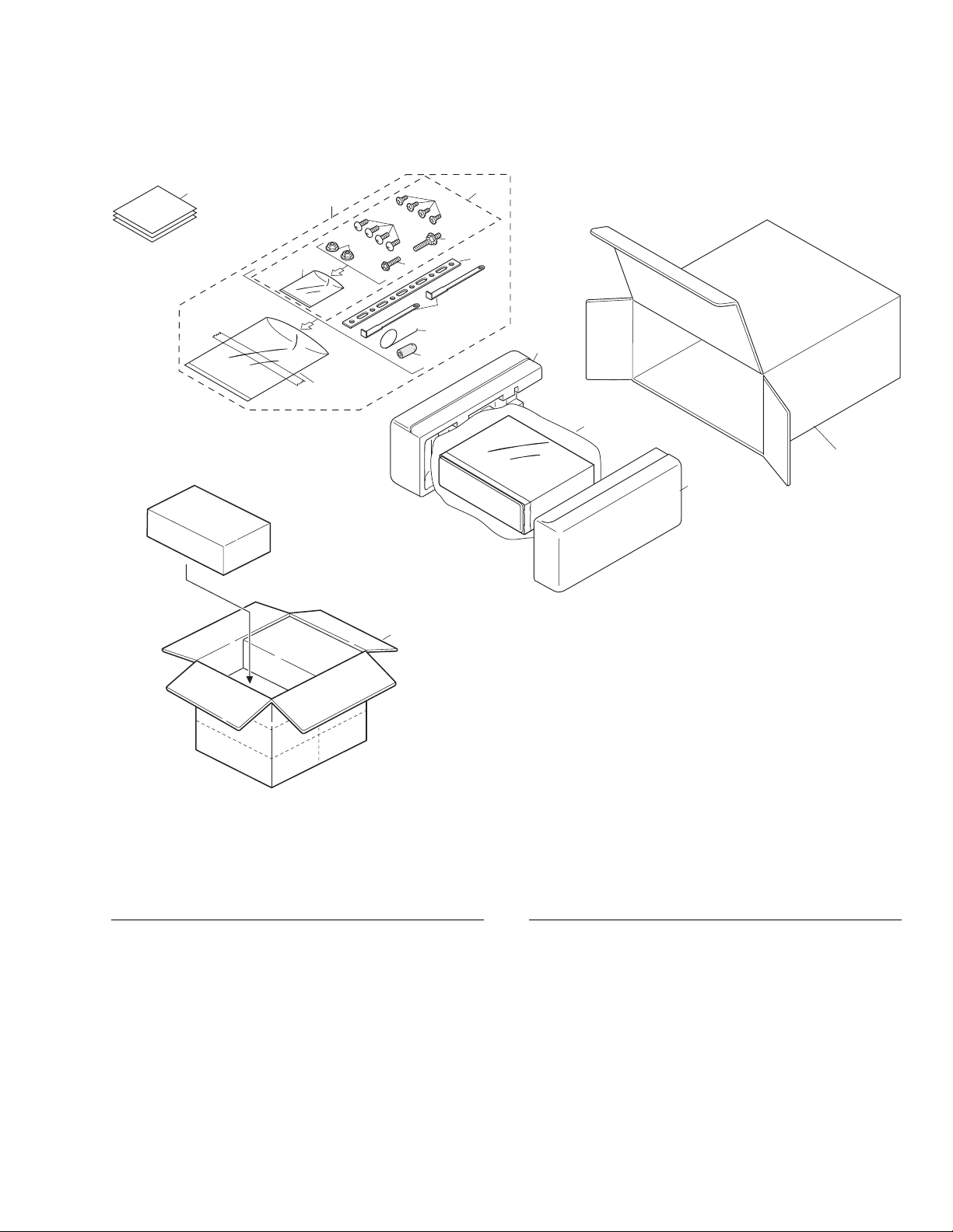
* 1 Card ARY1048
2 Accessory Assy CEA1918
3 Spring CBH-865
4 Screw Assy CEA1924
5 Screw CBA-102
6 Screw CBA1284
* 7 Polyethylene Sheet CNM4338
8 Screw(x4) CRZ50P090FMC
9 Nut(x2) NF50FMC
10 Screw(x4) TRZ50P080FMC
* 11 Polyethylene Bag CEG-158
12 Handle CNC5395
13 Strap CNF-111
14 Bush CNV1009
15 Polyethylene Bag CEG1173
16 Carton CHG3758
17 Contain Box CHL3758
18 Protector CHP1734
19 Protector CHP1735
20 Owner’s Manual(English) CRB1545
21 Installation Manual(English) CRB1546
3
CDS-P5000
16
17
15
19
18
4
8
14
3
13
12
11
10
7
5
6
9
2
1,20,21
2. EXPLODED VIEWS AND PARTS LIST
2.1 PACKING
- PACKING SECTION PARTS LIST
Mark No. Description Part No.
Mark No. Description Part No.
NOTE:
- Parts marked by "*"are generally unavailable because they are not in our Master Spare Parts List.
- Screws adjacent to
∇ mark on the product are used for disassembly.
Page 4
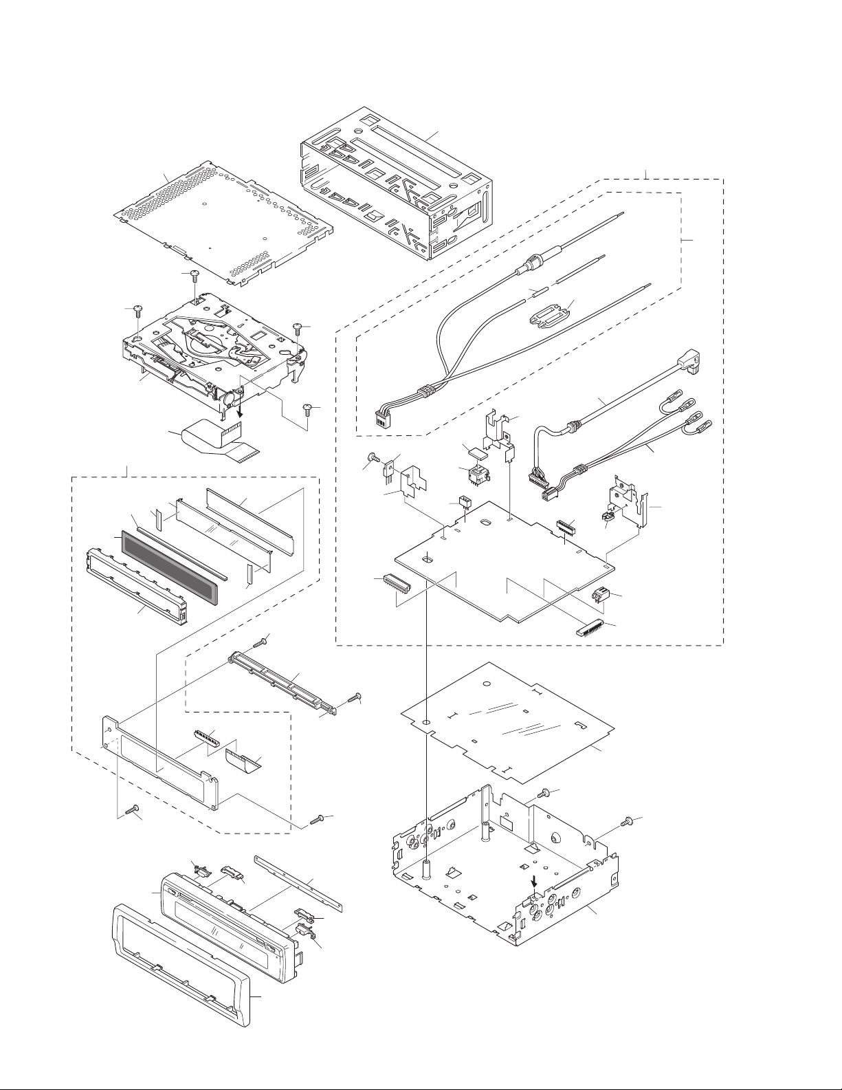
4
CDS-P5000
2.2 EXTERIOR
45
26
1
38
3
1
25
1
6
1
2
43
20
16
42
5
21
36
33
31
27
34
24
23
28
37
19
4
22
35
41
18
10
12
39
42
13
40
10
15
14
17
11
10
29
32
30
10
8
7
7
9
44
Page 5

5
CDS-P5000
1 Screw BSZ26P050FMC
2 Cable Assy CDE4869
3 Case CNB1795
4 Cord Assy CDE6012
5 Connector CNV5732
6
CD Mechanism Module(S7VA2) CXK5004
7 Screw BSZ30P050FMC
8 Insulator CNM6283
9 Chassis Unit CXB3838
10 Screw BPZ20P080FMC
11 Button(Eject) CAC6129
12 Button(D) CAC6130
13 Lighting Conductor CNV5729
14 Cover CNM4369
15 Holder CNV5731
16 Lighting Conductor CNV5728
17 Lighting Conductor CNV5730
18 Grille Unit CXB4057
19 Audio Control Unit CWM6371
20 Screw BSZ30P080FMC
21 Sheet CNM6181
22 Cord Assy CDE6001
23 Cord Assy CDE4862
24 Cap CNS1472
25 Resistor RS1/2PMF102J
26 LCD(LCD901) CAW1533
27 Connector(CN112) CKM1191
28 Plug(CN103) CKS1044
29 Connector(CN107) CKS1541
30 Connector(CN105) CKS2228
31 Connector(CN104) CKS3408
32 Plug(CN701) CKM1129
33 Spacer CNM6341
34 Holder CNC5321
35 Holder CNC5322
36 Holder CNC5323
37 Clamper CNV1335
38 Keyboard Unit CWM6373
39 Connector(CN901) CKS3118
40 Connector CDE4508
41 Holder CNC8452
42 Sheet CNM6189
43 Transistor(Q201) 2SD2396
44 Panel CNS5148
45 Holder CNC6798
- EXTERIOR SECTION PARTS LIST
Mark No. Description Part No.
Page 6
6
CDS-P5000
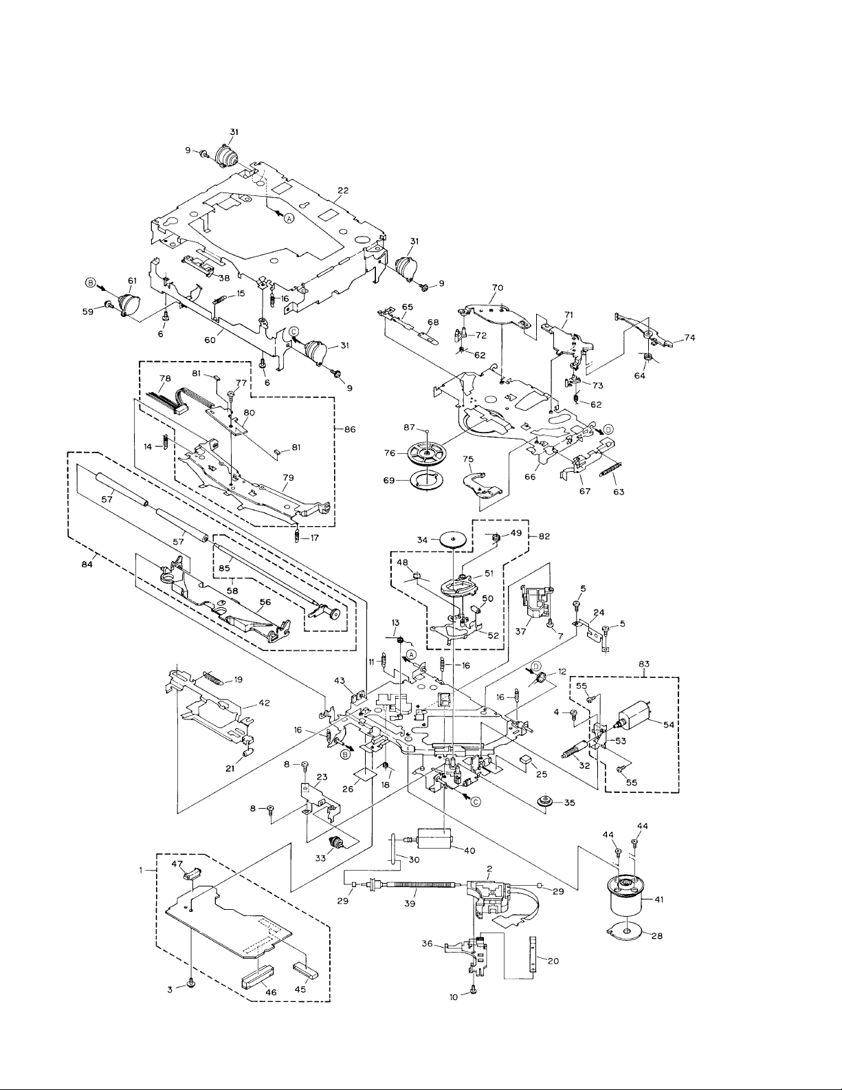
2.3 CD MECHANISM MODULE
Page 7

7
CDS-P5000
- CD MECHANISM MODULE SECTION PARTS LIST
1 Control Unit CWX2285
2 Pickup Unit(Service) CXX1230
3 Screw IMS26P035FMC
4 Screw BMZ20P025FMC
5 Screw BMZ20P040FMC
6 Screw BSZ20P040FMC
7 Screw CBA1077
8 Screw CBA1250
9 Screw CBA1296
10 Screw CBA1362
11 Spring CBH1724
12 Spring CBH1729
13 Spring CBH1730
14 Spring CBH1731
15 Spring CBH1732
16 Spring CBH1745
17 Spring CBH1848
18 Spring CBH1849
19 Spring CBH1939
20 Spring CBL1214
21 Roller CLA2627
22 Frame CNC5796
23 Bracket CNC5871
* 24 Bracket CNC6376
25 Cushion CNM3917
26 Sheet CNM4873
27 •••••
28 Gathering PCB(1/20) CNX3066
29 Bearing CNR1415
30 Belt CNT1071
31 Damper CNV3974
32 Gear CNV5854
33 Gear CNV5820
34 Gear CNV4857
35 Gear CNV5821
36 Holder CNV4663
37 Holder CNV5071
38 Guide CNV5823
39 Screw Unit(S7) CXB4265
40 CRG Motor Unit(S7)(M2) CXB3043
41 Motor Unit(M1) CXA8912
42 Lever Unit CXA9300
43 Chassis Unit CXB2574
44 Screw JFZ20P025FMC
45 Connector(CN101) CKS1953
46 Connector(CN701) CKS2774
47 Connector(CN801) CKS2196
48 Spring CBH1832
49 Spring CBH1833
50 Roller CLA2627
51 Arm CNV4136
52 Arm Unit CXA8565
53 Bracket CNC6056
54 Load Motor Unit(S7)(M3) CXA8702
55 Screw JFZ20P025FMC
56 Arm CNV4120
57 Roller CNV4509
58 Gear Unit(S7) CXA8701
59 Screw CBA1455
60 Frame CNC5797
61 Damper CNV3974
62 Spring CBH1736
63 Spring CBH1863
64 Spring CBH1945
65 Spring CBL1326
66 Arm CNC8364
67 Lever CNC6054
68 Spacer CNM3315
69 Sheet CNM4849
70 Arm CNV5031
71 Arm CNV4123
72 Arm CNV4124
73 Arm CNV4125
74 Arm CNV4138
75 Arm CNV5032
76 Clamper CNV5308
77 Screw CBA1250
78 Connector(CN1) CDE4576
79 Arm CNC7383
* 80 Gathering PCB CNX2445
81 Photo-transistor(Q1, 2) CPT-230S-X
82 ELBO Arm Assy(S7) CXA8889
83 Load Motor Assy(S7) CXA8891
84 LO Arm Assy(S7) CXA8892
85 Shaft CLA3133
86 Guide Arm Assy(S7) CXB1850
87 Ball CNR1189
Mark No. Description Part No. Mark No. Description Part No.
Page 8
8
CDS-P5000
A
1
234
B
C
D
12
34
A
B
C
AUDIO CONTROL UNIT
KEYBOARD UNIT
CD MECHANISM MODULE
A
A-a A-b
A-a
A-b
A-b
A-a
Large size
SCH diagram
Guide page
Detailed page
A-a
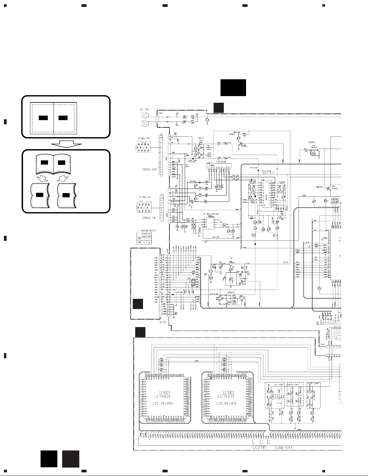
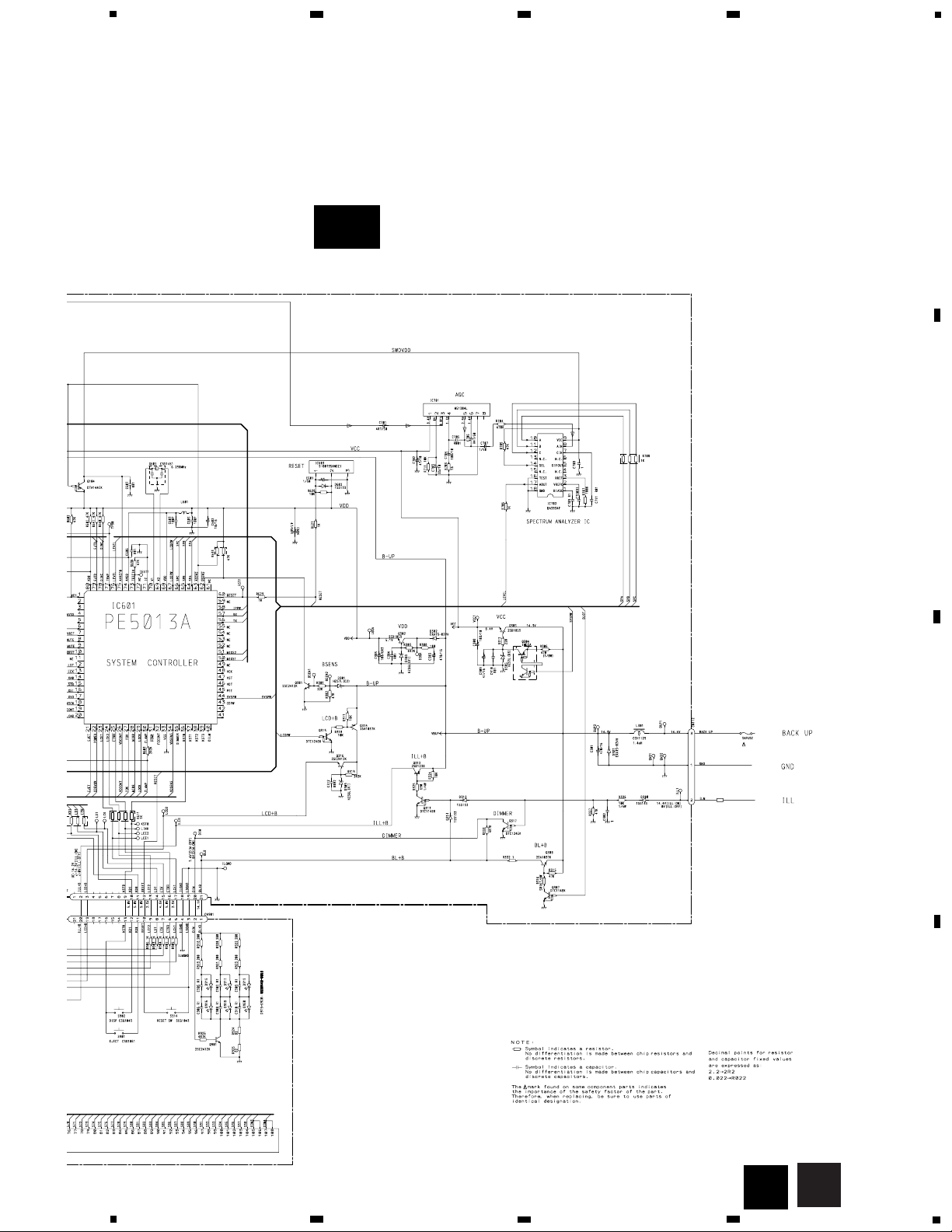
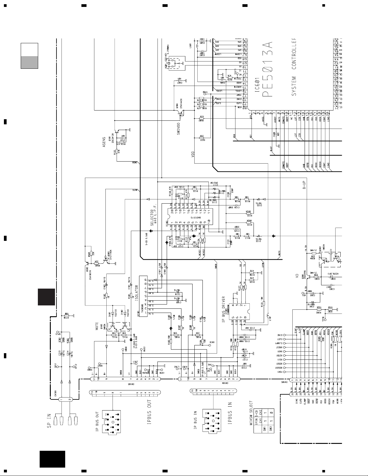
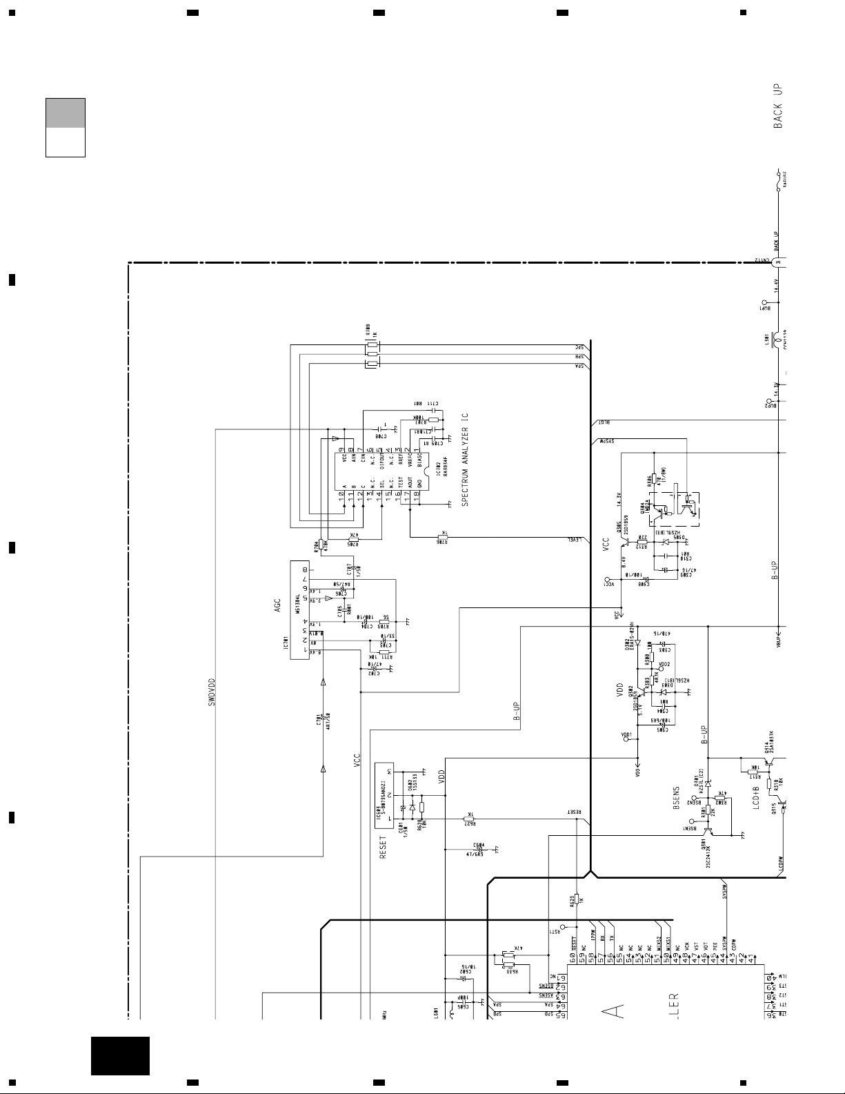
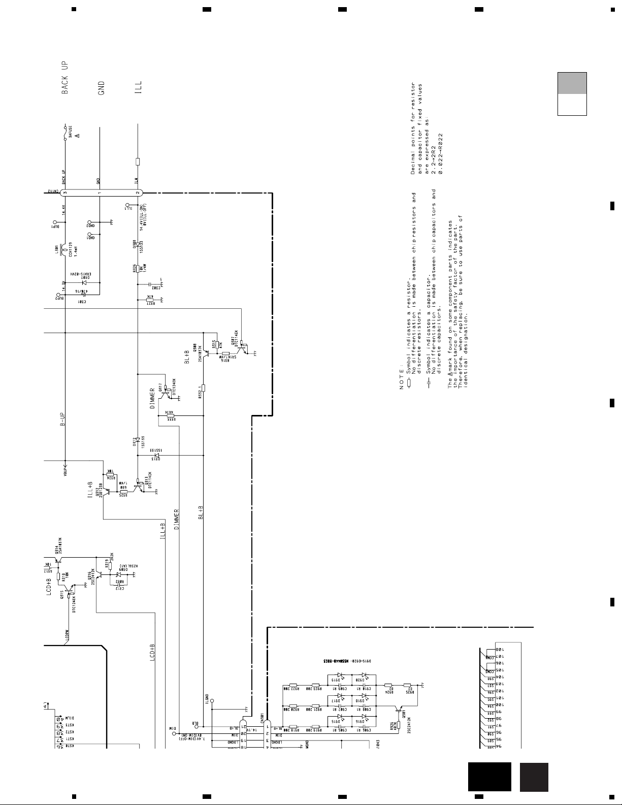
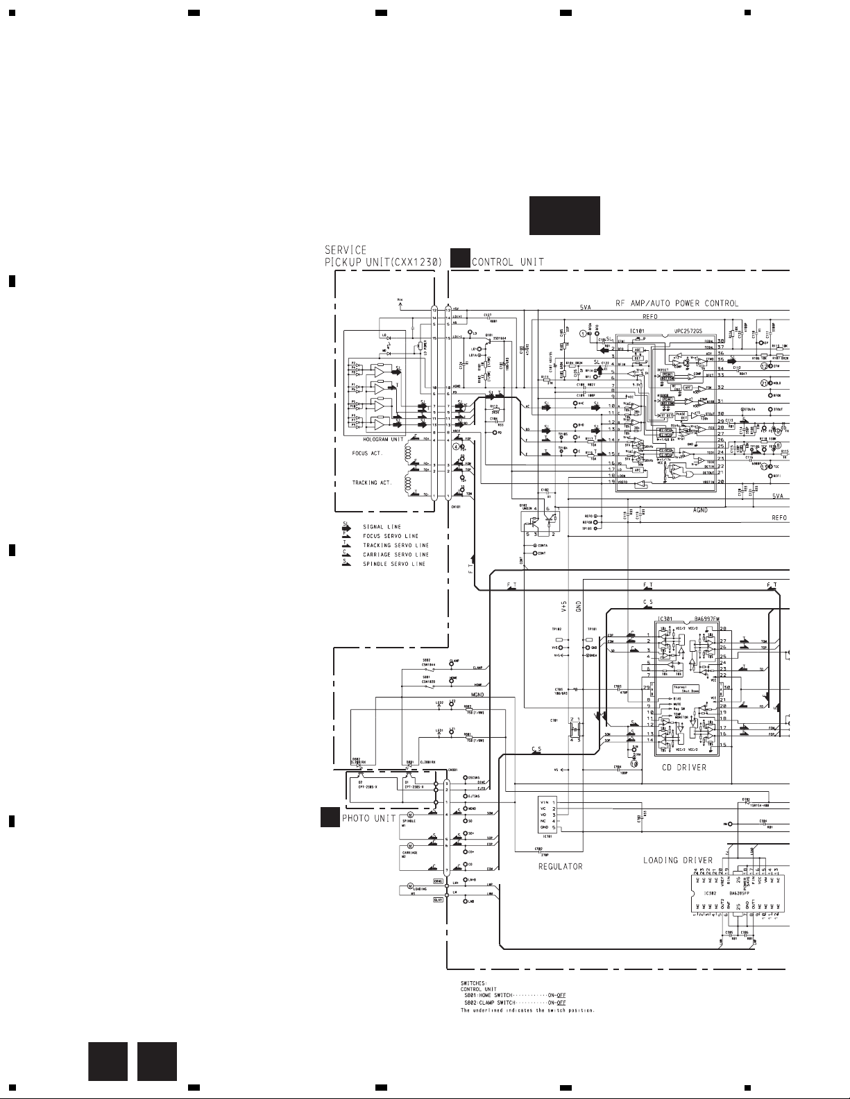
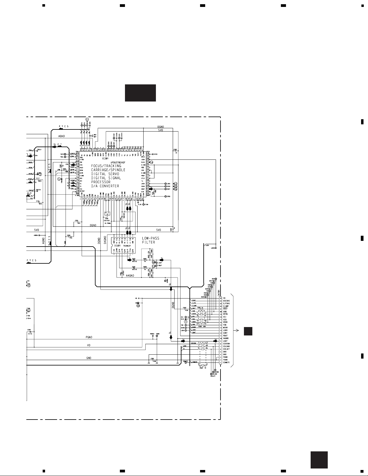
3. SCHEMATIC DIAGRAM
3.1 OVERALL CONNECTION DIAGRAM(GUIDE PAGE)
Note: When ordering service parts, be sure to refer to “EXPLODED VIEWS AND PARTS LIST” or “ELECTRICAL
PARTS LIST”.
B
Page 9
9
CDS-P5000
5
6
7
8
A
B
C
D
5
6
7
8
A
A-b
CEK1016
1K(1/2W)
LCD BACK LIGHT
B
Page 10
10
CDS-P5000
A
1
234
B
C
D
12
34
A
AUDIO CONTROL UNIT
ISM MODULE
A-a
A-b
A-a
Page 11
11
CDS-P5000
5
6
7
8
A
B
C
D
5
6
7
8
B
C
KEYBOARD UNIT
CD MECHANISM M
A-a
A-b
A-a
B
Page 12
12
CDS-P5000
A
1
234
B
C
D
1
2
34
A-a
A-b
A-b
CEK1016
Page 13
13
CDS-P5000
5
6
7
8
A
B
C
D
5
6
7
8
A-a
A-b
A-b
CEK1016
1K(1/2W)
LCD BACK LIGHT
B
Page 14
14
CDS-P5000
A
1
234
B
C
D
12
34
C
D
3.2 CD MECHANISM MODULE(GUIDE PAGE)
C-a
22/6R3
BA05SFP
CXA8912
CXB3043
CXA8702
C
D
Page 15
15
CDS-P5000
5
6
7
8
A
B
C
D
5
6
7
8
C-b
C
A
CN105
Page 16

16
CDS-P5000
A
1
234
B
C
D
12
34
C
C-a
C-a
C-b
Page 17

17
CDS-P5000
5
6
7
8
A
B
C
D
5
6
7
8
22/6R3
BA05SFP
CXA8912
CXB3043
CXA8702
D
C-a
C-a
C-b
D
Page 18

18
CDS-P5000
A
1
234
B
C
D
12
34
C-b
C-a
C-b
Page 19

19
CDS-P5000
5
6
7
8
A
B
C
D
5
6
7
C-b
8
C-a
C-b
A
CN105
Page 20

20
CDS-P5000
- Waveforms
1 RFO 0.5V/div. 0.5µs/div.
Normal mode: play
1 CH1: RFO 1V/div.
2 CH2: MIRR 5V/div.
Test mode: Tracking open
0.5ms/div.
1 CH1: RFO 1V/div.
2 CH2: MIRR 5V/div.
Normal mode: The defect part
passes 800µm
0.5ms/div.
3 CH1: FIN 0.5V/div.
4 CH2: FO+ 2V/div.
Test mode: No disc, Focus close
0.2s/div.
3 CH1: FIN 0.5V/div.
5 CH2: FOK 2V/div.
Normal mode: Focus close
0.2s/div.
6 CH1: FEY 0.5V/div.
7 CH2: XSI 2V/div.
Normal mode: Focus close
1ms/div.
REFO
→
8 CH1: TEY 0.5V/div.
9 CH2: TIN 0.5V/div.
Test mode: 32 tracks jump (FWD)
0.5ms/div.
8 CH1: TEY 0.5V/div.
9 CH2: TIN 0.5V/div.
Test mode: Single jump (FWD)
0.5ms/div.
8 CH1: TEY 0.5V/div.
9 CH2: TIN 0.5V/div.
Test mode: 100 tracks jump (FWD)
5ms/div.
6 CH1: FEY 0.1V/div.
3 CH2: FIN 0.2V/div.
Normal mode: Play
20ms/div.
3 CH1: FIN 0.5V/div.
0 CH2: SIN 1V/div.
Normal mode: Focus close (12cm)
0.5s/div.
3 CH1: FIN 0.5V/div.
0 CH2: SIN 1V/div.
Normal mode: Focus close (8cm)
0.5s/div.
GND
→
GND
→
REFO
→
REFO
→
REFO
→
REFO
→
GND
→
REFO
→
REFO
→
GND
→
REFO
→
REFO
→
REFO
→
REFO
→
REFO
→
REFO
→
REFO
→
REFO
→
REFO
→
REFO
→
REFO
→
REFO
→
Note:1. The encircled numbers denote measuring pointes in the circuit diagram.
2. Reference voltage
REFO:2.5V
Page 21

21
CDS-P5000
8 CH1: TEY 0.2V/div.
9 CH2: TIN 0.2V/div.
Normal mode: play
8 CH1: TEY 0.5V/div.
! CH2: SD 0.5V/div.
5ms/div.
0 SIN 0.5V/div. 0.1s/div.
Normal mode: Play (12cm)
0 SIN 0.5V/div. 10ms/div.
Long Search (12cm)
@ EFM 1V/div. 5µs/div.
Play
8 CH1: TEY 1V/div.
# CH2: TEC 1V/div.
Test mode: Focus close
Tracking open
2ms/div.
8 CH1: TEY 0.5V/div.
6 CH2: FEY 0.5V/div.
Normal mode: AGC after focus
close
0.2s/div.
$ PLCK 2V/div. 0.5µs/div.
Play
20ms/div.
% SCKO 2V/div. 1µs/div.
Play
^ Dout 2V/div. 10µs/div.
Play
& LRCK 2V/div. 20µs/div. * VD 5V/div. 50ms/div.
Normal mode: No disc
GND
→
REFO
→
REFO
→
GND
→
REFO
→
REFO
→
REFO
→
REFO
→
REFO
→
REFO
→
REFO
→
REFO
→
REFO
→
GND
→
REFO
→
GND
→
REFO
→
GND
→
REFO
→
GND
→
REFO
→
Page 22

22
CDS-P5000
( CH1: R OUT 1V/div.
) CH2: L OUT 1V/div.
Normal mode: Play (1kHz 0dB)
6 CH1: FEY 0.2V/div.
3 CH2: FIN 0.5V/div.
Normal mode: During AGC
1ms/div.
8 CH1: TEY 0.2V/div.
9 CH2: TIN 0.5V/div.
Normal mode: During AGC
1 CH1: RFO 1V/div.
⁄ CH2: HOLD 5V/div.
Normal mode: The defect part passes
800µm
0.2ms/div. 1ms/div.
0.5ms/div.
3 CH1: FIN 1V/div.
⁄ CH2: HOLD 5V/div.
Normal mode: The defect part passes
800µm
0.5ms/div.
GND
→
GND
→
REFO
→
REFO
→
REFO
→
REFO
→
REFO
→
REFO
→
Page 23

23
CDS-P5000
Page 24

24
CDS-P5000
A
1
234
B
C
D
12
34
A
4. PCB CONNECTION DIAGRAM
4.1 AUDIO CONTROL UNIT
Capacitor
Connector
P.C.Board
Chip Part
SIDE A
SIDE B
NOTE FOR PCB DIAGRAMS
1. The parts mounted on this PCB
include all necessary parts for
several destination.
For further information for
respective destinations, be sure
to check with the schematic diagram.
2. Viewpoint of PCB diagrams
AUDIO CONTROL UNIT
A
IPBUSIN
Page 25

25
CDS-P5000
5
6
7
8
A
B
C
D
5
6
7
8
A
SIDE A
CN901
CN701
C
IPBUSOUT
SPIN
B
Page 26

26
CDS-P5000
A
1
234
B
C
D
12
34
A
AUDIO CONTROL UNIT
A
Page 27

27
CDS-P5000
5
6
7
8
A
B
C
D
5
6
7
8
A
SIDE B
Page 28

28
CDS-P5000
A
1
234
B
C
D
12
34
4.2 KEYBOARD UNIT
SIDE A
KEYBOARD UNIT
B
B
RESET
EJECT
DISP
Page 29

29
CDS-P5000
1
2
3
4
A
B
C
D
1
2
3
4
SIDE B
CN107
A
KEYBOARD UNIT
B
B
Page 30

30
CDS-P5000
A
1
234
B
C
D
12
34
TEY
4.3 CD MECHANISM MODULE
C
CONTROL UNIT
C
CN105
A
PICKUP UNIT
(SERVICE)
C
PHOTO UNIT
D
D
SIDE A
CN801
Page 31

31
CDS-P5000
A
B
C
D
1
1
2
34
2
34
D
SIDE B
CONTROL UNIT
C
C
CLAMP
HOME
Page 32

32
CDS-P5000
5. ELECTRICAL PARTS LIST
NOTES:
- Parts whose parts numbers are omitted are subject to being not supplied.
- The part numbers shown below indicate chip components.
Chip Resistor
RS1/_S___J,RS1/__S___J
Chip Capacitor (except for CQS.....)
CKS....., CCS....., CSZS.....
=====Circuit Symbol and No.===Part Name Part No.
--- ------ ------------------------------------------ -------------------------
Unit Number: CWM6371
Unit Name : Audio Control Unit
IC 101 IC TA2050S
IC 102 IC BA3131FS
IC 103 IC CA0008AM
IC 601 IC PE5013A
IC 603 IC S-80735ANDZI
IC 701 IC M51304L
IC 702 IC BA3834F
Q 101 Transistor 2SC2412K
Q 103 Transistor IMH3A
Q 104 Transistor DTA144EK
Q 201 Transistor 2SD2396
Q 202 Transistor IMD2A
Q 203 Transistor IMH3A
Q 204 Transistor DTA114TK
Q 301 Transistor 2SC2412K
Q 302 Transistor 2SD1859
Q 304 Transistor IMD2A
Q 305 Transistor 2SD1859
Q 307 Transistor DTC114EK
Q 308 Transistor 2SA1037K
Q 312 Transistor 2SB1238
Q 313 Transistor DTC114EK
Q 314 Transistor 2SA1037K
Q 315 Transistor DTC124EK
Q 316 Transistor 2SC2412K
Q 317 Transistor DTC124EK
Q 502 Transistor 2SA1037K
Q 503 Transistor DTC114EK
D 101 Diode 1SS133
D 102 Diode 1SS133
D 201 Diode HZS9L(B1)
D 202 Diode 1SS133
D 203 Diode 1SS133
D 301 Diode HZS7L(C2)
D 302 Diode ERA15-02VH
D 303 Diode HZS6L(B1)
D 305 Diode HZS9L(B3)
D 307 Diode ERA15-02VH
D 308 Diode 1SS133
D 309 Diode HZS6L(A1)
D 312 Diode 1SS133
D 313 Diode 1SS133
D 602 Diode 1SS133
L 101 Inductor LAU3R3J
L 301 Choke Coil 1.4mH CTH1129
L 601 Inductor LAU100K
X 601 Radiator 6.290MHz CSS1451
RESISTORS
R 101 RS1/10S102J
R 102 RS1/10S102J
R 103 RS1/10S181J
R 104 RS1/10S181J
R 105 RS1/10S223J
R 106 RS1/10S223J
R 107 RS1/10S102J
R 108 RS1/10S102J
R 109 RS1/10S473J
R 110 RS1/10S473J
R 111 RS1/10S562J
R 112 RS1/10S562J
R 113 RS1/10S473J
R 114 RS1/10S473J
R 115 RS1/10S223J
R 116 RS1/10S223J
R 117 RS1/10S103J
R 118 RS1/10S103J
R 119 RS1/10S103J
R 120 RS1/10S103J
R 121 RS1/10S103J
R 122 RS1/10S103J
R 123 RS1/10S101J
R 124 RS1/10S101J
R 125 RS1/10S473J
R 126 RS1/10S473J
R 127 RS1/10S102J
R 128 RS1/10S102J
R 129 RS1/10S473J
R 130 RS1/10S473J
R 131 RS1/10S103J
R 132 RS1/10S822J
R 133 RS1/10S822J
R 134 RS1/10S102J
R 135 RS1/10S102J
R 201 RS1/10S152J
R 202 RS1/10S122J
R 203 RD1/4PU221J
R 204 RD1/4PU221J
R 205 RS1/10S681J
R 206 RA3C102J
R 301 RS1/10S223J
R 302 RS1/10S473J
R 303 RS1/10S472J
R 306 RS1/8S471J
R 308 RS1/10S101J
R 312 RS1/10S221J
R 315 RS1/10S473J
R 316 RD1/4PU512J
R 317 RS1/10S103J
=====Circuit Symbol and No.===Part Name Part No.
--- ------ ------------------------------------------ -------------------------
A
Page 33

33
CDS-P5000
R 318 RS1/10S103J
R 319 RS1/10S222J
R 324 RS1/10S103J
R 325 RD1/4PU681J
R 326 RD1/4PU103J
R 327 RS1/10S473J
R 332 RS1/10S1R0J
R 333 RS1/10S472J
R 502 RS1/10S223J
R 503 RS1/10S223J
R 601 RS1/10S473J
R 602 RS1/10S473J
R 603 RS1/10S222J
R 605 RA4C102J
R 611 RA4C102J
R 627 RS1/10S102J
R 628 RS1/10S103J
R 629 RS1/10S102J
R 633 RA2CQ473J
R 636 RS1/10S473J
R 637 RS1/10S223J
R 638 RS1/10S473J
R 640 RS1/10S473J
R 641 RS1/10S473J
R 701 RS1/10S682J
R 702 RS1/10S682J
R 703 RS1/10S560J
R 704 RS1/10S474J
R 705 RS1/10S473J
R 706 RS1/10S102J
R 707 RS1/10S104J
R 708 RA3C102J
R 710 RS1/10S101J
R 711 RS1/10S103J
CAPACITORS
C 101 CEJA100M16
C 102 CEJA100M16
C 103 CEJA1R0M50
C 104 CEJA1R0M50
C 105 CEJA1R0M50
C 106 CEJA1R0M50
C 107 CEJA1R0M50
C 108 CEJA1R0M50
C 109 CEJA100M16
C 110 CEJA100M16
C 115 CEJA101M10
C 116 CEJA101M10
C 117 CEJA2R2M50
C 118 CKSRYB103K50
C 121 CKSRYB103K50
C 122 CEJA100M16
C 123 CEJA100M16
C 125 CKSRYB103K50
C 126 CCSRCH390J50
C 127 CCSRCH390J50
C 128 CCSRCH391J50
C 129 CCSRCH391J50
C 130 CCSRCH391J50
C 131 CCSRCH391J50
C 134 CKSRYB102K50
C 135 CKSRYB102K50
C 136 CCSRCH471J50
C 137 CCSRCH471J50
C 201 CEJA101M10
C 202 CKSRYB102K50
C 203 CKSRYB473K16
C 301 470µF/16V CCH1183
C 302 CKSYB105K16
C 303 470µF/16V CCH1183
C 304 CKSRYB103K50
C 305 CEJA101M6R3
C 308 CEJA101M10
C 309 CEJA470M16
C 310 CKSRYB103K50
C 312 CKSRYB823K16
C 601 CEJA1R0M50
C 602 CEJA100M16
C 603 CCSRCH101J50
C 604 CEJA470M6R3
C 605 CCSRCH101J50
C 606 CKSRYB103K50
C 607 CKSRYB103K50
C 608 CKSRYB103K50
C 701 CEJA4R7M50
C 702 CEJA470M10
C 703 CEJA330M10
C 704 CEJA101M10
C 705 CKSRYB102K50
C 706 CEJAR47M50
C 707 CEJANP1R0M50
C 708 CKSQYB105K16
C 709 CKSQYB104K25
C 710 CKSQYB104K25
C 711 CKSRYB103K50
C 713 CEJA100M16
C 714 CEJA100M16
Unit Number : CWM6373
Unit Name : Keyboard Unit
MISCELLANEOUS
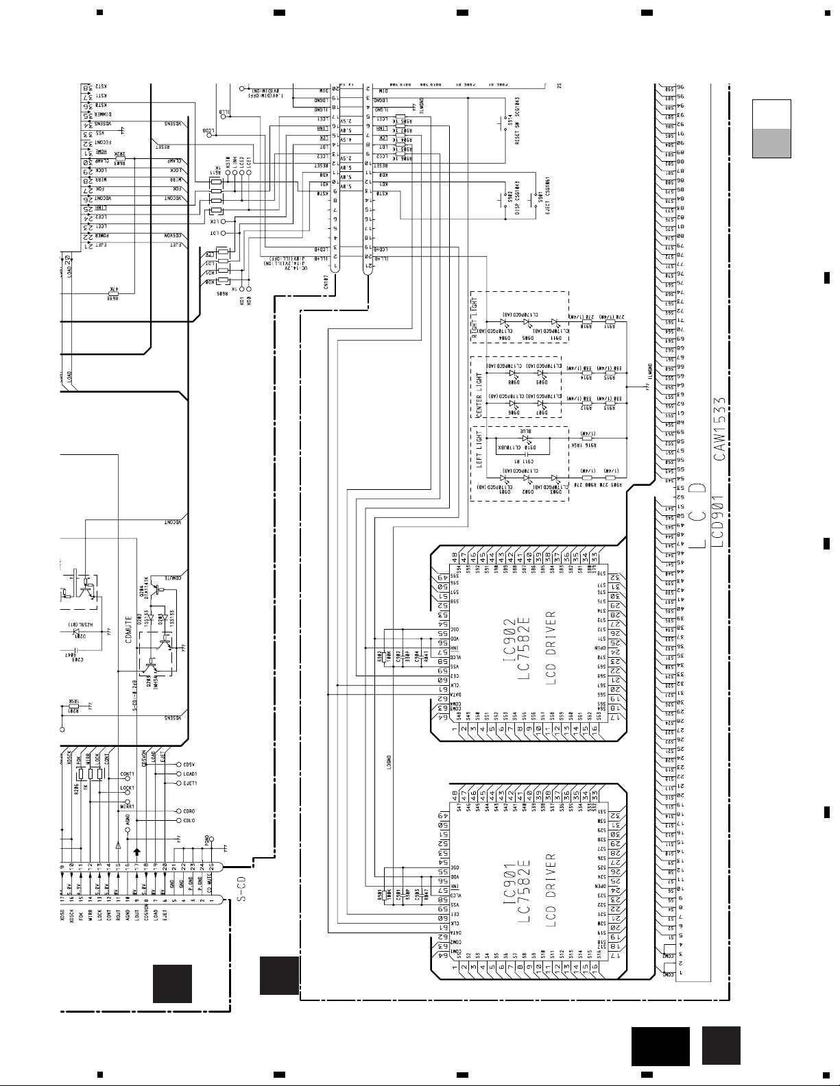
IC 901 IC LC7582E
IC 902 IC LC7582E
Q 901 Transistor 2SC2412K
D 901 LED CL170PGCD(AB)
D 902 LED CL170PGCD(AB)
D 903 LED CL170PGCD(AB)
D 904 LED CL170PGCD(AB)
D 905 LED CL170PGCD(AB)
D 906 LED CL170PGCD(AB)
D 907 LED CL170PGCD(AB)
D 908 LED CL170PGCD(AB)
D 909 LED CL170PGCD(AB)
D 910 LED CL170UBX
D 911 LED CL170PGCD(AB)
D 915 LED NSSW440-8063
D 916 LED NSSW440-8063
D 917 LED NSSW440-8063
D 918 LED NSSW440-8063
D 919 LED NSSW440-8063
D 920 LED NSSW440-8063
S 901 Switch(EJECT) CSG1061
S 902 Switch(DISP) CSG1043
S 914 Switch(HOME) CSG1043
LCD 901 LCD CAW1533
RESISTORS
R 901 RS1/10S104J
R 902 RS1/10S104J
R 903 RS1/10S102J
R 904 RS1/10S102J
R 905 RS1/10S102J
=====Circuit Symbol and No.===Part Name Part No.
--- ------ ------------------------------------------ -------------------------
=====Circuit Symbol and No.===Part Name Part No.
--- ------ ------------------------------------------ -------------------------
B
Page 34

34
CDS-P5000
R 906 RS1/10S102J
R 907 RS1/10S102J
R 908 RS1/4S271J
R 909 RS1/4S271J
R 910 RS1/4S271J
R 911 RS1/4S271J
R 912 RS1/4S331J
R 913 RS1/4S331J
R 914 RS1/4S331J
R 915 RS1/4S331J
R 916 RS1/4S152J
R 918 RS1/10S201J
R 919 RS1/10S201J
R 920 RS1/10S201J
R 921 RS1/10S201J
R 922 RS1/10S201J
R 923 RS1/10S201J
R 924 RS1/10S820J
R 925 RS1/10S820J
R 926 RS1/10S472J
CAPACITORS
C 901 CKSQYB331K50
C 902 CKSQYB331K50
C 903 CKSQYB473K25
C 904 CKSQYB473K25
C 905 CKSQYB104K50
C 906 CKSQYB104K50
C 907 CKSQYB104K50
C 908 CKSQYB104K50
C 909 CKSQYB104K50
C 910 CKSQYB104K50
C 911 CKSQYB104K50
Unit Number :CWX2285
Unit Name :Control Unit
MISCELLANEOUS
IC 101 IC UPC2572GS
IC 201 IC UPD63702AGF
IC 301 IC BA6997FM
IC 302 IC BA6285FP
IC 601 IC TA2063F
IC 701 IC BA05SFP
Q 101 Transistor 2SD1664
Q 102 Transistor UMD2N
D 701 Diode 1SR154-400
D 801 Chip LED CL200IRX
D 802 Chip LED CL200IRX
X 201 Ceramic Resonator 16.93MHz CSS1363
S 801 Switch (Home) CSN1028
S 802 Spring Switch (Clamp) CSN1044
RESISTORS
R 101 RS1/8S100J
R 102 RS1/8S120J
R 103 RS1/16S102J
R 104 RS1/16S822J
R 105 RS1/16S682J
R 106 RS1/16S183J
R 107 RS1/16S822J
R 108 RS1/16S333J
R 109 RS1/16S683J
R 110 RS1/16S134J
R 111 RS1/16S273J
R 112 RS1/16S222J
R 113 RS1/16S103J
R 114 RS1/16S103J
R 115 RS1/16S102J
R 116 RS1/16S163J
R 117 RS1/16S163J
R 201 RS1/16S104J
R 202 RS1/16S473J
R 501 RS1/16S0R0J
R 505 RS1/16S102J
R 507 RA3C102J
R 508 RA4C681J
R 601 RS1/16S102J
R 602 RS1/16S102J
R 603 RS1/16S223J
R 604 RS1/16S223J
R 801 RS1/8S751J
R 802 RS1/8S751J
CAPACITORS
C 101 CEV101M6R3
C 102 CKSQYB104K16
C 103 CEV470M6R3
C 104 CKSYB334K16
C 105 CCSRCH330J50
C 106 CKSRYB103K25
C 107 CEV4R7M35
C 108 CKSQYB273K50
C 109 CCSRCH101J50
C 110 CKSQYB104K16
C 111 CKSRYB332K50
C 112 CKSQYB473K16
C 113 CKSRYB103K25
C 114 CKSRYB391K50
C 115 CCSRCH121J50
C 116 CKSRYB682K50
C 117 CKSRYB333K16
C 118 CKSYB334K16
C 119 CKSYB334K16
C 120 CKSYB334K16
C 121 CKSYB334K16
C 122 CKSQYB104K16
C 123 CKSRYB472K50
C 124 CKSQYB104K16
C 125 CCSRCH6R0D50
C 126 CKSRYB153K25
C 127 CCSRCH102J25
C 201 CKSYB334K16
C 202 CKSQYB104K16
C 203 CKSQYB104K16
C 303 CEV470M16
C 304 CKSRYB103K25
C 305 CKSRYB103K25
C 306 CKSRYB103K25
C 307 CEV100M25
C 502 CKSRYB471K50
C 601 CEV101M6R3
C 602 CKSQYB104K16
C 603 CEV4R7M35
C 604 CEV4R7M35
C 605 CKSRYB152K50
C 606 CKSRYB152K50
C 607 CEV220M6R3
C 701 22µF/6.3V CCH1300
C 702 CKSYB334K16
=====Circuit Symbol and No.===Part Name Part No.
--- ------ ------------------------------------------ -------------------------
=====Circuit Symbol and No.===Part Name Part No.
--- ------ ------------------------------------------ -------------------------
C
Page 35

35
CDS-P5000
C 703 CEV101M6R3
C 901 CCSRCH471J50
C 902 CCSRCH271J50
C 903 CCSRCH471J50
C 904 CCSRCH101J50
Unit Number :
Unit Name :Photo Unit
Q 1 Photo-transistor CPT-230S-X
Q 2 Photo-transistor CPT-230S-X
Miscellaneous Parts List
Pickup Unit (Service) CXX1230
M 1 Motor Unit (Spindle) CXA8912
M 2 CRG Motor Unit CXB3043
M 3 Load Motor Unit CXA8702
=====Circuit Symbol and No.===Part Name Part No.
--- ------ ------------------------------------------ -------------------------
D
Page 36

36
CDS-P5000
• Note :
Unlike previous CD mechanism modules the grating angle of the PU unit cannot be adjusted after the PU unit is
changed. The PU unit in the CD mechanism module is adjusted on the production line to match the CD mechanism module and is thus the best adjusted PU unit for the CD mechanism module. Changing the PU unit is thus
best considered as a last resort. However, if the PU unit must be changed, the grating should be checked using
the procedure below.
• Purpose :
To check that the grating is within an acceptable range.
• Symptoms of Mal-adjustment :
If the grating is off by a large amount symptoms such as being unable to close tracking, being unable to perform
track search operations, or track searching taking a long time, may appear.
• Method :
• Measuring Equipment • Oscilloscope, Two L.P.F.
• Measuring Points • E, F, REFOUT
• Disc • ABEX TCD-784
• Mode • TEST MODE
• Checking Procedure
1. In test mode, load the disc and switch the 5V regulator on.
2. Using the FF and REV buttons, move the PU unit to the innermost track.
3. Press key 9 to close focus, the display should read "91". Press key 8 to implement the tracking balance adjust-
ment the display should now read "81". Press key 9 4 times. The display will change, returning to "81" on the
fourth press.
4. As shown in the diagram above, monitor the LPF outputs using the oscilloscope and check that the phase differ-
ence is within 75° . Refer to the photographs supplied to determine the phase angle.
5. If the phase difference is determined to be greater than 75° try changing the PU unit to see if there is any
improvement. If, after trying this a number of times, the grating angle does not become less than 75° then the
mechanism should be judged to be at fault.
• Note
Because of eccentricity in the disc and a slight misalignment of the clamping center the grating waveform may be
seen to "wobble" ( the phase difference changes as the disc rotates). The angle specified above indicates the average angle.
• Hint
Reloading the disc changes the clamp position and may decrease the "wobble".
100kW
390pF
100kW
390pF
E
REFOUT
F
REFOUT
Xch Ych
L.P.F.
L.P.F.
6. ADJUSTMENT
6.1 CHECKING THE GRATING AFTER CHANGING THE PICKUP UNIT
Oscilloscope
CONTROL UNIT
Page 37

37
CDS-P5000
Grating waveform
Ech → Xch 20mV/div, AC
Fch → Ych 20mV/div, AC
45°
0°
75°
60°
30°
90°
Page 38

38
CDS-P5000
- Pin Functions (PE5013A)
Pin No. Pin Name I/O Function and Operation
1 KD1 I Key return input
2,3 NC Not used
4 AVSS I A/D GND
5 NC Not used
6 BLGT O LCD back light control output
7 AVREF I A/D converter reference voltage
8 MUTE O Mute output
9 CDMUTE O CD mute output
10 xrst O CD LSI reset output
11 NC Not used
12 LDT O Data output for LCD driver
13 lck O Clock output for LCD driver
14 XAO O CD LSI data discernment control signal output
15 stb O LSI Strobe output
16 XSI I Serial input (CD)
17 XSO O Serial output (CD)
18 XSCK O LSI clock output
19 CONT O Server driver power control output (CD)
20 LOAD O Loading motor LOAD control
21 EJECT O CD loading motor LOAD control output
22 POWER O CD +5V control
23 LCE1 O Chip enable output pin for LCD driver
24 LCE2 O Chip enable output pin for LCD driver
25 linh O Inhibit output for LCD driver
26 VDCONT O VD control output
27 FOK I FOK signal input
28 MIRR I Mirror detector input
29 LOCK I Spindle lock detector input
30 CLAMP I Disc clamp sense input
31,32 NC Not used
33 VSS GND
34 VDIN I VD sense input
35 NC Not used
36 KST0 Key strobe output
37–43 NC Not used
44 SYSPW O System power control output
45–49 NC Not used
50,51 MIXS1,2 O Mixing switch select output
52–55 NC Not used
56 TX O IP BUS data output
57 RX I IP BUS data input
58 ippw O Power supply control output for IP BUS interface IC
59 NC Not used
60 reset Reset
61 NC Not used
62 bsens I Back Up sense input
63 asens I ACC power sense input
64 SPA O Clock output for spectrum analyzer
65 SPB O MONO/STEREO select output for spectrum analyzer
66 SPC O Strobe signal output for spectrum analyzer
67 LCDPW O LCD back light power supply control output
68 VDD Power voltage
69 X2 Crystal oscillator connection pin
7. GENERAL INFORMATION
7.1 PARTS
7.1.1 IC
Page 39

Pin No. Pin Name I/O Function and Operation
70 X1 Crystal oscillator connection pin
71 IC Connect to GND
72 NC Not used
73 TESTIN I Test program mode input
74 AVDD A/D converter analog power supply (VDD)
75 AVREF0 GND
76 LEVEL I Level input for spectrum analyzer
77 TEMP Temperature detector
78 DINC I Disc insert sense input
79 EJTD I Disc eject position sense input (CD)
80 KD0 I Key return input
39
CDS-P5000
IC's marked by* are MOS type.
Be careful in handling them because they are very
liable to be damaged by electrostatic induction.
*PE5013A
20
21
40
41
60
61
80
1
BA3834F
BIASC
VREFC
RREF
N.C
DIFOUT
N.C
CIN
AIN
VCC 9
PEAK
HOLD
PEAK
HOLD
PEAK
HOLD
PEAK
HOLD
PEAK
HOLD
PEAK
HOLD
PEAK
HOLD
BIAS
VREF
RES
RES
RES
MPX
RES
RES
RES
RES
DEC
1
2
3
68Hz
BPF
4
170Hz
BPF
A-C
5
6
C
7
8
DIF
A
420Hz
BPF
1kHz
BPF
2.4kHz
BPF
5.9kHz
BPF
14.4kHz
BPF
REFERENCE CURRENT
18
17
16
15
14
13
12
11
10
GND
AOUT
TEST
N.C
SEL
N.C
C
B
A
Page 40

40
CDS-P5000
7.1.2 DISPLAY
- CAW1533
Page 41

41
CDS-P5000
7.2 DIAGNOSIS
7.2.1 DISASSEMBLY
- Removing the Case(Not shown)
1. Open the case by using a screwdriver and remove it.
- Removing the Grille Assy(Not shown)
1. Release the Grille Assy from the hooks and pull it out.
- Removing the CD Mechanism Module(Not shown)
1. Remove the four fixing screws.
2. Disconnect the connector, and then remove the CD Mech
Module.
- Removing the Audio Control Unit(Fig.1)
Remove the two screws.
Straighten the four hooks marked with an arrow.
Lift up the Audio Control Unit to remove it.
Audio Control Unit
Fig.1
Do not
remove
the damper.
Remove frame B
and pull out the
mechanism unit.
All these springs
are the same type.
Be careful
not to catch
on other parts.
- Removing the Damper and the Frame Unit(Fig.2)
Fig.2
Page 42

42
CDS-P5000
Be careful.
This work requires
considerable force
and involves the danger
of injury.
Turn the support wheel
so that the screw head
become visible through
the hole.
Each spring
is different
type.
After raising
the guide arm
90˚, remove it.
Stand the back
side of the arm,
lift up the left
then remove.
The loading motor
is soldered on
the PCB.
- Removing the Spindle Motor(Fig.3)
Fig.2
- Removing the Loading Motor(Fig.4)
Fig.4
Page 43

43
CDS-P5000
Attach the
short pin to
protect the
PU unit.
Be careful
not to drop
the bearing.
Be careful
to handle
the tab.
Remove
the holder
by sliding.
- Removing the PU Unit and the Carriage Motor(Fig.5)
Fig.5
Page 44

44
CDS-P5000
7.2.2 TEST MODE
1)Precautions
• This unit uses a single power supply (+5V) for the
regulator. The signal reference potential, therefore, is
connected to REFO(approx. 2.5V) instead of GND.
If REFO and GND are connected to each other by mistake during adjustments,not only will it be impossible
to measure the potential correctly,but the servo will
malfunction and a severe shock will be applied to the
pick-up. To avoid this,take special note of the following.
Do not connect the negative probe of the measuring
equipment to REFO and GND together. It is especially
important not to connect the channel 1 negative
probe of the oscilloscope to REFO with the channel 2
negative probe connected to GND.
Since the frame of the measuring instrument is usually at the same potential as the negative probe,change
the frame of the measuring instrument to floating status.
If by accident REFO comes in contact with
GND,immediately switch the regulator or power OFF.
• Always make sure the regulator is OFF when connecting and disconnecting the various filters and wiring
required for measurements.
• Before proceeding to further adjustments and measurements after switching regulator ON,let the player
run for about one minute to allow the circuits to stabilize.
• Since the protective systems in the unit’s software are
rendered inoperative in test mode,be very careful to
avoid mechanical and /or electrical shocks to the system when making adjustment.
• This unit is adjusted in a combination with the CD
control unit (KEH-P7000, etc.). Each regulator key
should be operated at the unit.
With the KEH-P7000 taken up for reference, a description will be given below concerning how to enter into
the test mode, including key operations. The key in
the adjustment text is also one of the KEH-P7000
keys.
• How to enter into the test mode
Switch ACC,back-up ON while pressing the 4 and 6
keys together.
• Resetting the test mode
Switch ACC,back-up Off.
• Disc detection during loading and eject operations is
performed by means of a photo transistor in this
unit.Consequently,if the inside of the unit is exposed
to a strong light source when the outer casing is
removed for repairs or adjustment,the following malfunctions may occur.
*During PLAY, even if the eject button is pressed,the
disc will not be ejected and the unit will remain in
the PLAY mode.
*The unit will not load a disc.
When the unit malfunctions this way,either re-position the light source,move the unit or cover the
photo transistor.
• When loading and unloading discs during adjustment
procedures,always wait for the disc to be properly
clamped or ejected before pressing another key.
Otherwise, there is a risk of the actuator being
destroyed.
• Turn power off when pressing the button FF or the
button REV key for focus search in the test mode. (Or
else lens may stick and the actuator may be damaged.)
• SINGLE/4TRK/10TRK/32TRK will continue to operate
even after the key is released.Tracking is closed the
moment C-MOVE is released.
• JUMP MODE resets to SINGLE as soon as power is
switched off.
Page 45

45
CDS-P5000
- Flow Chart
Tracking offset
BAND
46
BAND
912
ACC, Back-up ON
SOURCE
12
7
BAND
12
BAND
BAND
8
7
7
FF REV
REV
12
8
9 FF REV
98
00"00'
TRACK FUNCTION
FF
912FF7REV BAND
TRACK
00"00'00
FUNCTION
00"00'
TRACK FUNCTION
00"00'
TRACK FUNCTION
*1
00"00'
TRACK FUNCTION
Display
*2
*3
<Carriage MOVE
or T.jump>
*3 *4
<AGC display
select>
*5
<AGC >
<Tracking open>
00"00'
TRACK FUNCTION
Display
< Mechanism test mode in >
Display
TRACK
91"91'91
FUNCTION
TRACK
81"81'81
FUNCTION
TRACK
56"02'1
FUNCTION
0X"00'72
<ELV,TRAY select>
<Operation mode
select >
<Shift > <Shift >
*6 *9*8*7
<Mechanism test
mode out >
*1 Normal focus close S curve check Focus EQ check
*3 100 TRK jump and carriage MOVE continue only while the keys are released
*4 SINGLE
*2 Normal display Focus cancel Tracking balance
*5 Normal display Focus gain Tracking gain Focus bias
(Close spindle-rough)
<Carriage MOVE
or T.jump>
4TRK 10TRK 32TRK 100TRK C.MOVE
Display
81 8685848382
*6 ELV motor select
*7
Display
TRAY motor select
0X"10'72
TRACK
00"00'72
FUNCTION
00"00'72 01"00'72 02"00'72
8ms pulse drive
Display
24ms pulse drive DC drive
*8
00"10'72
01"10'72 02"10'72
48ms pulse drive
Display
100ms pulse drive DC drive
ELV select : ELV dowm (Disc 1
→ 6)
TRAY select : TRAY out
*9 ELV select : ELV up (Disc 6
→ 1)
TRAY select : TRAY in
00"00'00 01"01'01 02"02'02
Display
<CD multi player selected>
<Focus mode
select>
<Auto adjustment
display>
AGC YES
<Power OFF>
<T.jump mode
change>
Display
example
<Power OFF>
Display
Display
Display
Display Display
<Tracking closed >
<Tracking
closed >
AGC NO
<Tracking
closed >
<Carriage shifted
outwards while
this key is pressed>
<Carriage shifted
inwards while
this key is pressed>
<Carriage shifted
outwards while
this key is pressed>
<Carriage shifted
inwards while
this key is pressed>
<Focus closed>
<Power OFF>
<Power ON>
Display
During regulator off, press the 12
key and the system will be put into
the new test mode.
<Tracking open >
<New test mode in>
<Power OFF>
Page 46

46
CDS-P5000
- New Test Mode(aging operation and setup analysis)
The single CD player plays in normal mode. After being set up, it will display FOK (focus), LOCK (spindle), subcode,
sound skip, protection against a mechanical error or the like, occurrence of an error, cause and time of an expiry, if
any, (and disc number)
During the setup, the CD software operation status (internal RAM and C-point)is displayed.
(1) How to enter NEW TEST Mode
See the test mode flow chart Page 45.
(2) Relations of keys between TEST and NEW TEST Modes
Keys Test Mode New Test Mode
Regulator OFF Regulator ON PLAY in progress Error Occurred,
Protection Activated
BAND Regulator ON Regulator OFF Time of occurrence/
cause of error select
FF FWD-Kick FF/TRACK+
REV REV-Kick REV/TRACK-
7 Tracking close SCAN
8 Tracking open MODE
9 Focus close
12 To New Test Jump Mode AUTO/MANU TRACK No./
Mode Select time of occurrence select
Operations,such as EJECT, CD ON/OFF, etc. are performed normally
(3) Error Cause (Error Number) Code
Error Code Classification Mode Description Cause/Detail
40 ELECTRIC PLAY FOK=L Put out of focus
100ms Scratch,
41 ELECTRIC PLAY LOCK=L Spindle unlock Stain,
100ms Vibration,
42 ELECTRIC PLAY Subcode Failed to read subcode Servo defect,
unacceptable 500ms etc...
43 ELECTRIC PLAY Sound skipped Last address memory
operated
(4) Indicating an Operation Status During Setup
Status No. Description Protection operation
01 Carriage home mode started None
02 Carriage moving inwards 10-second time out, Home switch failed
03 Carriage moving outwards 10-second time out, Home switch failed
05 Carriage moving outwards None
11 Setup started None
12 Spindle turn/Focus search started None
13 Waiting for focus closure (XSI=L) Failure to close focus
10,14 Waiting for focus closure (FOK=H) Failure to close focus
15, 16, 17 Focus closed, Tracking open Focus disrupted
18 During focus AGC Focus disrupted
19 During tracking AGC Disrupted focus
20 Waiting for MIRR, LOCK or subcode read Focus disrupted, MIRR NG, Failure to lock,
Carriage closed, SPINDLE=ADAPTIVE failed to read subcode
Page 47

47
CDS-P5000
(5) Example of Display.
•SET UP in progress
8 digits display LCD
•Operation (PLAY, SEARCH, etc.) in progress perfectly
identical with that in the normal mode.
•Protection/Error upon occurrence(8 digits display LCD)
(a) Error number indicated
Select the display with the
BAND key.
(b) Track number and
absolute time indicated
ERROR–xx
- Error Number Indication
If the CD should fail to operate or if an error has taken place during operation the player will enter into the error
mode, and the cause of the error will be numerically indicated.
This is aimed at assisting in analysis or repair.
(1) Basic Means of Display
•Examples of Display ERROR-xx
(2) Error Codes
Error Classification Description Cause/Detail
Code
10 ELECTRIC Carriage home failure Carriage doesn't move to or from the innermost position
tHome switch failed and/or carriage immobile
11 ELECTRIC Focus failure Focus failed
tDefects, disc upside-down, severe vibration
12 ELECTRIC SETUP failure Spindle failed to lock or subcode unreadable
Subcode failure tSpindle defective, defect, severe vibration
14 ELECTRIC Mirror failure Unrecorded CD-R
The disc is upside-down, defects, vibration
17 ELECTRIC Set up failure AGC protect failed
tDefects, disc upside-down, severe vibration
19 ELECTRIC Set up failure Tracking error waveform is too unbalanced (>50%) or
level is too small
tThe pickup unit or tracking error circuitry is N.G.
30 ELECTRIC Search time out Failed to reach target address
tCarriage/tracking defective and/or defects
A0 SYSTEM Power failure Power overvoltage or short circuit detected
tSwitching transistor defective and/or power abnormal
A1 SYSTEM Mechanism power Mechanism elevation reference voltage is out of
failure prescription
tEREF adjustment VR and/or power abnormal
50 MECHANISM An error upon ejection MAG switch release time has time out
Elevation time out when eject
60 MECHANISM An error while putting in Tray in / out time has time out
and out the tray Tray is caught when put in
70 MECHANISM An error upon elevation Elevation time has time out
80 MECHANISM An error with an empty No disc is available
magazine inserted
* Setup means a series of operations after focusing up to sound output.
TNo.11Min11Sec
11
TNo.10Min40Sec
05
Page 48

48
CDS-P5000
LCD LCD901
LC7582E
IC901
LC7582E
IC902
S1-S47 S48-S98
1
5656
19
LCD+B
20
ILL+B
D901-911
LIGHT
D915-920
13
12 11
S902
S901
S914
10
3
2
LCD BACK LIGHT
CN701
CN901
CN107
IC701
M51304L
AGC
LCD DRIVER
LCD DRIVER
3
SP IN
IC702
BA3834F
SPECTRUM ANALYZER IC
5
817
IC601
PE5013A
76
LEVEL
SYSTEM
CONTROLLER
SPA,SPB,SPC
IP-BUS IN
CN104
IC101
TA2050S
7
11
1
2
L+
L-
1
5
BUS+
BUS-
ISOLATOR
1
2
IP-BUS OUT
CN103
7
L+
1
5
BUS+
BUS-
IC102
BA3131FS
SELECTOR and
L.P.F.
3
1
17
4
2
3
20
19
18
1
3
LOUT
IC103
CA0008AM
IP-BUS DRIVER
6
5
VDD
7
RX,TX,IPPW
CD5VON
LOAD
EJECT
EJTD
DINC
CD5VON
LOAD
EJECT
EJTD
DINC
CLAMPCLAMP
78
79
21
20
22
CD5VON
LOAD
EJECT
EJTD
CLAMP
DINC
30
2,6,7
IC603
S-80735ANDZI
RESET
1
60
VDD
2
Q103
Q502
8 MUTE
3
CN112
Q302
VDD
Q201
Q202
26
VDCONT
9
10 11
12
KST0
KD1
KD0
RESET
136 80 60
VCC
5
VCC
11
VCC
1
BACK UP
ILL
Q312
Q313
2
2
3
Q316
Q314
Q315
67
LCDPW
Q317
VCC
Q305
Q307
Q308
EJECT
DISP
RESET
MUTE
VD
ILL+B
LCD+B
DIMER
VCC
BL+B
9
22
24
23
6
7
8
25
IC601
TA2063F
IC101
UPC25720GS
IC301
BA6997FM
6
1019
IC201
UPD63702GF
SERVO/DSP
X201
10
11
S802
CLAMP
S801
HOME
74
IC701
BA05SFP
IC302
BA06285FP
VD
2
1
5V REGULATOR
3
V+5
19
17
5
8
RF AMP
4CH
SERVO DRIVER
FDTDMD
SD
17
Q101
16
26
4
2
15
6
4
2
15
6
16
HOLOGRAM
UNIT
+5V
LD
GND
MD
FOCUS ADT
TRACKING ACT
M
M
2
1
14
13
7
6
5
4
3
2
CARRIAGE
MOTOR
SPINDOLE
MOTOR
M
LOADING
MOTOR
A
AUDIO CONTROL UNIT
B
KEYBOARD UNIT
C
CONTROL UNIT
D
PHOTO UNIT
PICKUP UNIT
(SERVICE)
6
BLGT
44
SYSPW
7.3 BLOCK DIAGRAM
Page 49

49
CDS-P5000
8. OPERATIONS AND SPECIFICATIONS
Connection Diagram
+
White
Left
≠
White/black
White/black
Front speaker
Right
+
≠
Gray
Gray/black
Gray/black
+
Green
Left
≠
Green/black
Rear speaker
Right
+
Violet
Violet/black
≠
Head unit
IP-BUS (Blue)
(sold separately)
This unit
IP-BUS input
(Blue)
IP-BUS input
(Blue)
IP-BUS (Blue)
Black (ground)
Fuse resistor
Orange
Fuse holder
Yellow
Multi-CD player
(sold separately)
To vehicle (metal) body.
To lighting switch terminal.
To terminal always supplied
with power regardless of
ignition switch position.
Page 50

8.1 OPERATIONS
CDS-P5000
Key Finder
DISPLAY button Disc loading slot EJECT button
RESET button
General
Power source .......... 14.4 V DC (10.8 – 15.1 V allowable)
Grounding system ........................................ Negative type
Max. current consumption ........................................ 1.1 A
Dimensions
(DIN) (mounting size)
........................ 178 (W) × 50 (H) × 145 (D) mm
[7 (W) × 2 (H) × 5-3/4 (D) in]
(nose) ................ 188 (W) × 58 (H) × 18 (D) mm
[7-3/8 (W) × 2-1/4 (H) × 3/4 (D) in]
(D) (mounting size)
........................ 178 (W) × 50 (H) × 150 (D) mm
[7 (W) × 2 (H) × 5-7/8 (D) in]
(nose) ................ 170 (W) × 46 (H) × 13 (D) mm
[6-3/4 (W) × 1-3/4 (H) × 1/2 (D) in]
Weight ........................................................ 1.2 kg (2.7 lbs)
CD player
System .................................... Compact disc audio system
Usable discs .................................................. Compact disc
Signal format .................... Sampling frequency: 44.1 kHz
Number of quantizatin bits: 16; linear
Frequency characteristics .............. 5 – 20,000 Hz (±1 dB)
Signal-to-noise ratio ...... 92 dB (1 kHz) (IHF-A network)
Dynamic range ............................................ 90 dB (1 kHz)
Number of channels ............................................ 2 (stereo)
8.2 SPECIFICATIONS
 Loading...