

Page 1
PIONEER CORPORATION 4-1, Meguro 1-chome, Meguro-ku, Tokyo 153-8654, Japan
PIONEER ELECTRONICS (USA) INC. P.O. Box 1760, Long Beach, CA 90801-1760, U.S.A.
PIONEER EUROPE NV Haven 1087, Keetberglaan 1, 9120 Melsele, Belgium
PIONEER ELECTRONICS ASIACENTRE PTE. LTD. 253 Alexandra Road, #04-01, Singapore 159936
PIONEER CORPORATION 2003
CDJ-1000MK2
COMPACT DISC PLAYER
CDJ-1000MK2
THIS MANUAL IS APPLICABLE TO THE FOLLOWING MODEL(S) AND TYPE(S).
Model Type Power Requirement Remarks
CDJ-1000MK2 KUCXJ AC120V
CDJ-1000MK2 TLXJ AC110- 240V
CDJ-1000MK2 WYXJ AC220- 240V
ORDER NO.
RRV2802
For details, refer to "Important symbols for good services"
T-ZZY JULY 2003 printed in Japan
Page 2
1234
SAFETY INFORMATION
A
This service manual is intended for qualified service technicians ; it is not meant for the casual do-ityourselfer. Qualified technicians have the necessary test equipment and tools, and have been trained
to properly and safely repair complex products such as those covered by this manual.
Improperly performed repairs can adversely affect the safety and reliability of the product and may
void the warranty. If you are not qualified to perform the repair of this product properly and safely, you
should not risk trying to do so and refer the repair to a qualified service technician.
WARNING
This product contains lead in solder and certain electrical parts contain chemicals which are known to the state of California to cause
cancer, birth defects or other reproductive harm.
B
NOTICE
(FOR CANADIAN MODEL ONLY)
Fuse symbols (fast operating fuse) and/or (slow operating fuse) on PCB indicate that replacement par ts must
be of identical designation.
REMARQUE
(POUR MODÈLE CANADIEN SEULEMENT)
Les symboles de fusible (fusible de type rapide) et/ou (fusible de type lent) sur CCI indiquent que les pièces
de remplacement doivent avoir la même désignation.
C
Health & Safety Code Section 25249.6 – Proposition 65
(FOR USA MODEL ONLY)
1. SAFETY PRECAUTIONS
The following check should be performed for the
continued protection of the customer and service
technician.
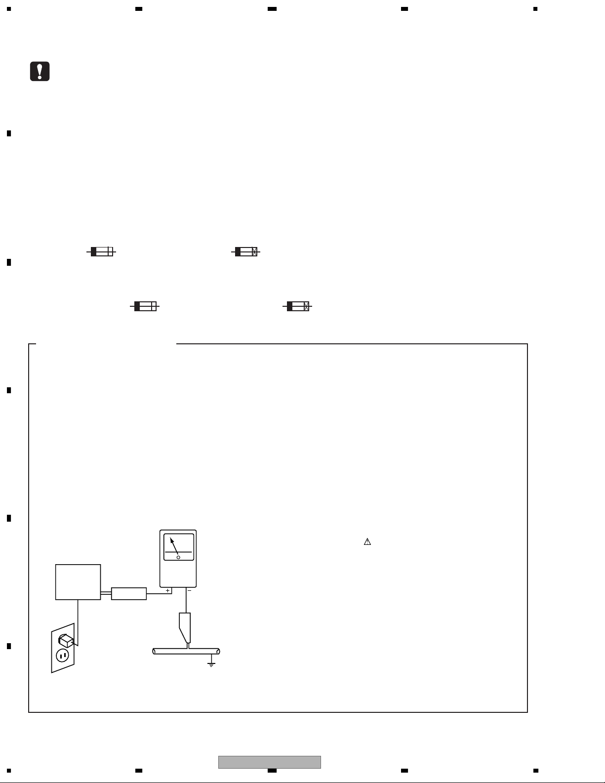
LEAKAGE CURRENT CHECK
Measure leakage current to a known earth ground (water
pipe, conduit, etc.) by connecting a leakage current tester
D
E
such as Simpson Model 229-2 or equivalent between the
earth ground and all exposed metal parts of the appliance
(input/output terminals, screwheads, metal overlays, control
shaft, etc.). Plug the AC line cord of the appliance directly
into a 120V AC 60Hz outlet and turn the AC power switch
on. Any current measured must not exceed 0.5mA.
Reading should
not be above
0.5mA
Earth
ground
Device
under
test
Also test with
plug reversed
(Using AC adapter
plug as required)
Test all
exposed metal
surfaces
Leakage
current
tester
ANY MEASUREMENTS NOT WITHIN THE LIMITS
OUTLINED ABOVE ARE INDICATIVE OF A POTENTIAL
SHOCK HAZARD AND MUST BE CORRECTED BEFORE
RETURNING THE APPLIANCE TO THE CUSTOMER.
2. PRODUCT SAFETY NOTICE
Many electrical and mechanical parts in the appliance
have special safety related characteristics. These are
often not evident from visual inspection nor the protection
afforded by them necessarily can be obtained by using
replacement components rated for voltage, wattage, etc.
Replacement parts which have these special safety
characteristics are identified in this Service Manual.
Electrical components having such features are identified
by marking with a
in this Service Manual.
The use of a substitute replacement component which does
not have the same safety characteristics as the PIONEER
recommended replacement one, shown in the parts list in
this Service Manual, may create shock, fire, or other hazards.
Product Safety is continuously under review and new
instructions are issued from time to time. For the latest
information, always consult the current PIONEER Service
Manual. A subscription to, or additional copies of, PIONEER
Service Manual may be obtained at a nominal charge from
PIONEER.
on the schematics and on the parts list
AC Leakage Test
F
2
1234
CDJ-1000MK2
Page 3
5678
IMPORTANT
THIS PIONEER APPARATUS CONTAINS
LASER OF CLASS 1.
SERVICING OPERATION OF THE APPARATUS
SHOULD BE DONE BY A SPECIALLY
INSTRUCTED PERSON.
LASER DIODE CHARACTERISTICS
MAXIMUM OUTPUT POWER: 5 mW
WAVELENGTH: 780 – 785 nm
WARNING !
The AEL(accessible emission level) of the laser power output is less then CLASS 1
but the laser component is capable of emitting radiation exceeding the limit for
CLASS 1.
A specially instructed person should servicing operation of the apparatus.
LABEL CHECK
CDJ-1000MK2/ WYXJ Type OnlyCDJ-1000MK2/ TLXJ Type Only
Printed on the Bottom Plate 2.
Bottom Plate 2
∗ : Refer to page 68.
1. Laser Interlock Mechanism
The position of the switch (S510) for detecting loading
completion is detected by the system microprocessor,
and the design prevents laser diode oscillation when the
switch is not in LPS1 terminal side (when the mechanism
is not clamped and LPS1 signal is high level.)
Thus, the interlock will no longer function if the switch is
deliberately set to LPS1 terminal side. ( if LPS1 signal is
low level ).
In the test mode* the interlock mechanism will not function.
Laser diode oscillation will continue, if pin 4 of AN8702NFH
(IC800) on the MAIN ASSY is connected to GND, or else
the terminals of Q600 are shorted to each other (fault
condition).
2. When the cover is opened, close viewing of the objective
lens with the naked eye will cause exposure to a Class 1
laser beam.
Additional Laser Caution
A
B
C
D
E
F
56
CDJ-1000MK2
7
8
3
Page 4
1234
[ Important symbols for good services ]
In this manual, the symbols shown-below indicate that adjustments, settings or cleaning should be made securely.
When you find the procedures bearing any of the symbols, be sure to fulfill them:
A
1. Product safety
You should conform to the regulations governing the product (safety, radio and noise, and other regulations), and
should keep the safety during servicing by following the safety instructions described in this manual.
2. Adjustments
To keep the original performances of the product, optimum adjustments or specification confirmation is indispensable.
In accordance with the procedures or instructions described in this manual, adjustments should be performed.
3. Cleaning
B
For optical pickups, tape-deck heads, lenses and mirrors used in projection monitors, and other parts requiring cleaning,
proper cleaning should be performed to restore their performances.
4. Shipping mode and shipping screws
To protect the product from damages or failures that may be caused during transit, the shipping mode should be set or
the shipping screws should be installed before shipping out in accordance with this manual, if necessary.
5. Lubricants, glues, and replacement parts
Appropriately applying grease or glue can maintain the product performances. But improper lubrication or applying
glue may lead to failures or troubles in the product. By following the instructions in this manual, be sure to apply the
prescribed grease or glue to proper portions by the appropriate amount.For replacement parts or tools, the prescribed
ones should be used.
C
D
E
F
4
1234
CDJ-1000MK2
Page 5

5678
CONTENTS
1. SPECIFICATIONS.............................................................................................................................................6
2. EXPLODED VIEWS AND PARTS LIST.............................................................................................................7
2.1 PACKING ....................................................................................................................................................7
2.2 EXTERIOR SECTION (1/2)........................................................................................................................8
2.3 EXTERIOR SECTION (2/2)......................................................................................................................10
2.4 SLOT-IN MECHANISM SECTION ............................................................................................................12
2.5 TRAVERSE MECHANISM ASSY-S ..........................................................................................................13
3. BLOCK DIAGRAM AND SCHEMATIC DIAGRAM ..........................................................................................14
3.1 BLOCK DIAGRAM....................................................................................................................................14
3.2 OVERALL WIRING DIAGRAM .................................................................................................................16
3.3 MAIN (1/4) and SPCN ASSYS .................................................................................................................18
3.4 MAIN (2/4), FLRB and SLMB ASSYS ......................................................................................................20
3.5 MAIN (3/4) and MMCB ASSYS ................................................................................................................22
3.6 MAIN ASSY (4/4)......................................................................................................................................24
3.7 DABB, JACB and DOUT ASSYS..............................................................................................................26
3.8 MFLB (1/2) and RSWB ASSYS................................................................................................................28
3.9 MFLB (2/2) ASSY .....................................................................................................................................30
3.10 KSWB and SLDB ASSYS.......................................................................................................................31
3.11 JFLB and JOGB ASSYS.........................................................................................................................32
3.12 SW POWER SUPPLY and PSWB ASSYS .............................................................................................34
4. PCB CONNECTION DIAGRAM ......................................................................................................................42
4.1 MAIN ASSY ..............................................................................................................................................42
4.2 SPCN, STCN, FLRB, SLMB and MMCB ASSYS.....................................................................................46
4.3 DABB, JACB and DOUT ASSYS..............................................................................................................48
4.4 MFLB and RSWB ASSYS ........................................................................................................................50
4.5 KSWB ASSY.............................................................................................................................................54
4.6 SLDB ASSY..............................................................................................................................................55
4.7 JFLB and JOGB ASSYS...........................................................................................................................56
4.8 SW POWER SUPPLY and PSWB ASSYS ...............................................................................................58
5. PCB PARTS LIST............................................................................................................................................59
6. ADJUSTMENT ................................................................................................................................................64
7. GENERAL INFORMATION .............................................................................................................................65
7.1 DIAGNOSIS..............................................................................................................................................65
7.1.1 SERVICE MODE................................................................................................................................65
7.1.2 DISASSEMBLY ..................................................................................................................................75
7.1.3 On Discharge of the Capacitor...........................................................................................................80
7.1.4 CLEANING.........................................................................................................................................80
7.1.5 POWER ON SEQUENCE ..................................................................................................................81
7.2 PARTS ......................................................................................................................................................84
7.2.1 IC........................................................................................................................................................84
8. PANEL FACILITIES .........................................................................................................................................93
A
B
C
D
56
CDJ-1000MK2
E
F
7
8
5
Page 6
1234
1. SPECIFICATIONS
CDJ-1000MK2/ KUCXJ type
1. General
A
System ................................................................. Compact disc digital audio system
Power requirements ........................................................................... AC 120 V, 60 Hz
Power consumption ............................................................................................ 33 W
Operating temperature ...................................................................... +5 ˚C – +35 ˚C
Operating humidity .....................................................................................5% – 85%
(There should be no condensation of moisture.)
Weight ................................................................................................ 4.2 kg (9.26 lb)
Dimensions ........................................................
12 – 5/8 (W) x 14 – 9/16 (D) x – 1/8 (H) in
2. Audio section
Frequency response .............................................................................. 4 Hz – 20 kHz
B
Signal-to-noise ratio ............................................................ 115 dB or more (JEITA)
Distortion ............................................................................................ 0.006% (JEITA)
CDJ-1000MK2/ TLXJ type
1. General
System ................................................................. Compact disc digital audio system
Power requirements ............................................................ AC 110–240 V, 50/60 Hz
Power consumption ............................................................................................ 31 W
Operating temperature ........................................................................ +5˚C – +35˚C
Operating humidity .....................................................................................5% – 85%
(There should be no condensation of moisture.)
C
Weight ................................................................................................................ 4.2 kg
Dimensions ........................................................ 320 (W) x 370 (D) x 105 (H) mm
2. Audio section
Frequency response .............................................................................. 4 Hz – 20 kHz
Signal-to-noise ratio ............................................................ 115 dB or more (JEITA)
Distortion ............................................................................................0.006% (JEITA)
320 (W) x 370 (D) x 105 (H) mm
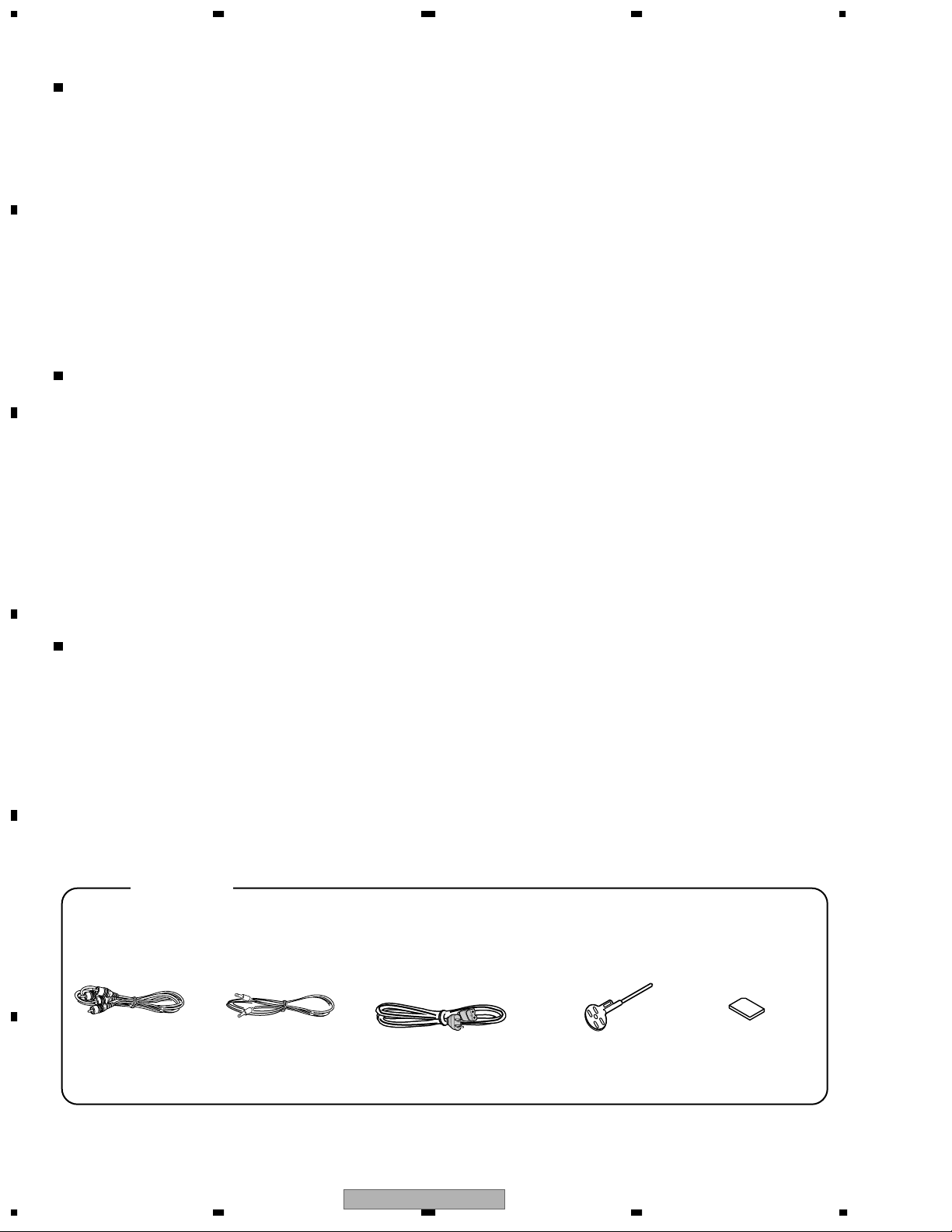
3. Accessories
Operating instructions ........................................................................................ 1
Power cord ........................................................................................................... 1
Audio cable .......................................................................................................... 1
Control cord ........................................................................................................ 1
Forced eject pin (housed in a groove in the bottom panel) ............................ 1
Multimedia Card (MMC) (16 MB) .................................................................... 1
Limited warranty ................................................................................................. 1
NOTE:
Specifications and design are subject to possible modification without notice.
3. Accessories
Operating instructions ........................................................................................ 1
Power cord ........................................................................................................... 1
Audio cable .......................................................................................................... 1
Control cord ........................................................................................................ 1
Forced eject pin (housed in a groove in the bottom panel) ............................ 1
Multimedia Card (MMC) (16 MB) .................................................................... 1
NOTE:
Specifications and design are subject to possible modification without notice.
CDJ-1000MK2/ WYXJ type
1. General
System ................................................................. Compact disc digital audio system
Power requirements ...............................................................AC 220-240V, 50/60 Hz
Power consumption ............................................................................................ 31 W
D
Operating temperature ........................................................................ +5˚C – +35˚C
Operating humidity .....................................................................................5% – 85%
(There should be no condensation of moisture.)
Weight ................................................................................................................ 4.2 kg
Dimensions ........................................................ 320 (W) x 370 (D) x 105 (H) mm
2. Audio section
Frequency response .............................................................................. 4 Hz – 20 kHz
Signal-to-noise ratio ............................................................ 115 dB or more (JEITA)
Distortion ............................................................................................ 0.006% (JEITA)
Accessories
E
Audio Cable
(VDE1064) L=1.5m
Control Cord
(PDE-319) L=1 m
3. Accessories
Operating instructions ........................................................................................ 1
Power cord ........................................................................................................... 1
Audio cable .......................................................................................................... 1
Control cord ........................................................................................................ 1
Forced eject pin (housed in a groove in the bottom panel) ............................ 1
Multimedia Card (MMC) (16 MB) .................................................................... 1
NOTE:
Specifications and design are subject to possible modification without notice.
Power Cord
(KUCXJ type : ADG7021
(TLXJ, WYXJ type: ADG1154)
Forced Eject Pin
(DEX1013)
MMC Memory Card
(DWX2326)
F
6
1234
CDJ-1000MK2
Page 7
2
7
11
10
9
13
8
12
15
14
4
6
5
1
3
5678
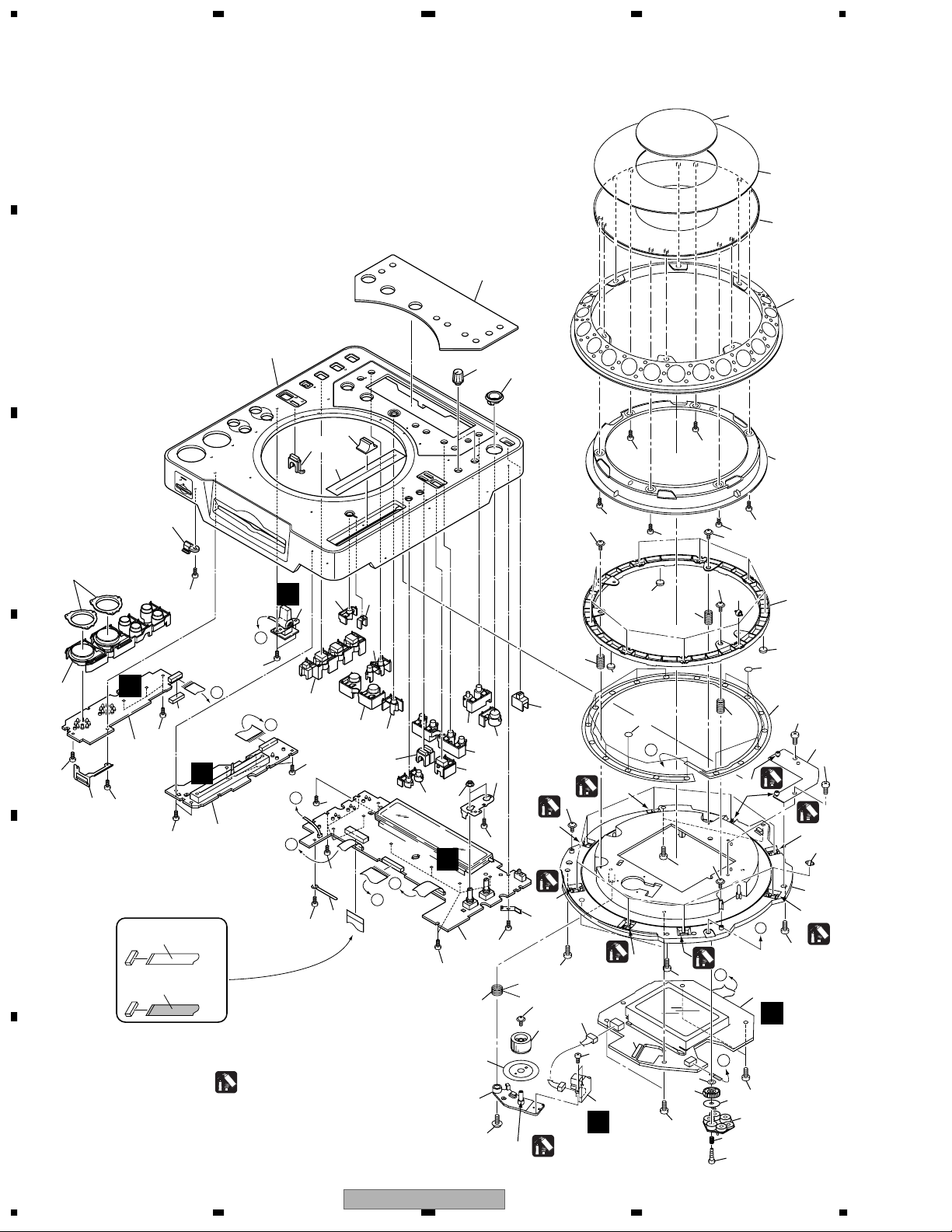
2. EXPLODED VIEWS AND PARTS LIST
NOTES:
Parts marked by "NSP" are generally unavailable because they are not in our Master Spare Parts List.
The mark found on some component parts indicates the importance of the safety factor of the part.
Therefore, when replacing, be sure to use parts of identical designation.
Screws adjacent to mark on product are used for disassembly.
For the applying amount of lubricants or glue, follow the instructions in this manual.
(In the case of no amount instructions, apply as you think it appropriate.)
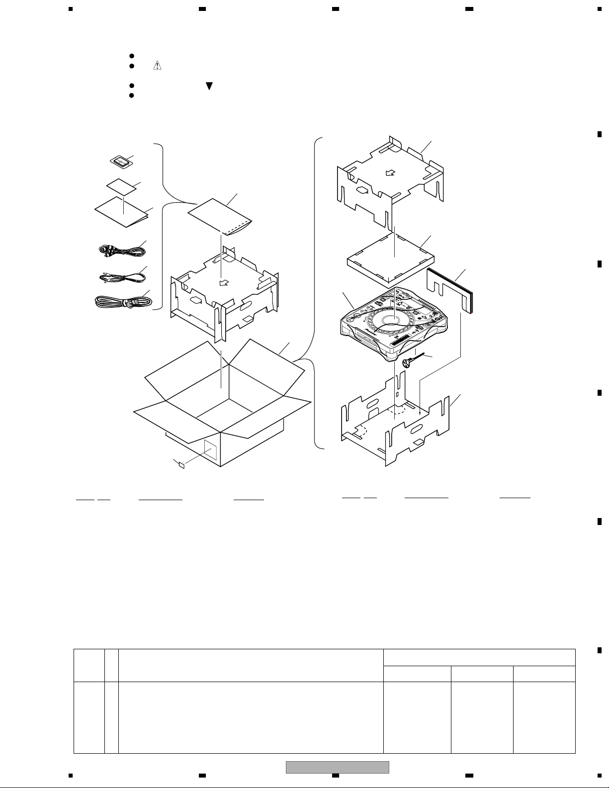
2.1 PACKING
A
B
C
PACKING Parts List
Mark
Mark
No. Description Part No.
1 Power Cord See Contrast Table(2)
>
NSP 2 Warranty Card See Contrast Table(2)
3 Forced Eject Pin DEX1013
4 Operating Instructions See Contrast Table(2)
5 Control Cord (L= 1m) PDE-319
6 Audio Cable (L= 1.5m) VDE1064
NSP 7 Polyethylene Bag Z21-038
(230 x 340 x 0.03)
No. Description Part No.
8 Pad (A) DHA1533
9 Pad (B) DHA1534
10 Pad (C) DHA1535
11 Pad (D) DHA1536
12 Packing Case See Contrast Table(2)
13 Sheet RHX1006
NSP 15 Label VRW1629
14 MMC Memory Card DWX2326
(2) CONTRAST TABLE
CDJ-1000MK2/KUCXJ, TLXJ and WYXJ types are constructed the same except for the following:
Mark No. Symbol and Description
> 1 Power Cord ADG7021 ADG1154 ADG1154
NSP 2 Warranty Card ARY7043 Not used Not used
4 Operating Instructions (English) DRB1339 Not used Not used
4 Operating Instructions (English, Spanish, Chinese) Not used DRB1340 Not used
4 Operating Instructions (English, French, German, Italian, Dutch, Spanish) Not used Not used DRB1338
12 Packing Case DHG2363 DHG2364 DHG2362
KUCXJ type TLXJ type WYXJ type
Part No.
D
E
F
56
CDJ-1000MK2
7
8
7
Page 8
1234
2.2 EXTERIOR SECTION (1/2)
A
TLXJ Type Only
51
B
WYXJ Type Only
46
50
44
C
33
25
33
B
3
D
31
25
K
13
47
L
Refer to
"2.3 Exterior (2/2) section".
40
47
39
47
15
23
26
5
J
E
C
33
14
4
F
18
25
G
30
10
Q
47
55
55
47
47
27
36
I
6
F
A
H
2
38
M
25
33
37
47
47
47
47
47
D
32
55
55
56
56
48
28
C
47
47
29
49
47
P
11
47
M
48
H
47
47
17
E
37
B
D
G
7
8
47
I
9
Refer to
" 2.4 Slot -IN Mechanism section".
34
48
NON-CONTACT
SIDE
E
CONTACT SIDE
F
24
8
1234
47
I
45
12
19
H
47
1
A
F
415352
48
G
53
54
43
41
48
K
J
A
L
41
CDJ-1000MK2
47
16
21
20
35
42
22
C
D
E
B
48
Page 9
5678
EXTERIOR SECTION (1/2) Parts List
Mar
k No. Description Part No.
1 MAIN Assy DWX2303
2 MMCB Assy DWX2304
3 SPCN Assy DWX2170
4 STCN Assy DWX2171
5 SLMB Assy DWX1309
6 PSWB Assy
7 DABB Assy DWX2305
8 JACB Assy DWX2306
9 DOUT Assy DWX2307
10 FLRB Assy DWX2308
11 SW POWER SUPPLY Assy DWR1370
12 25P Flexible Cable/60V DDD1196
13 12P Flexible Cable/60V DDD1197
14 4P Flexible Cable/60V DDD1198
15 Earth Lead Unit/300V DDF1024
16 Connector Assy 3P DKP3562
17 Connector Assy 6P DKP3654
18 FPC D5 Slot DNP1948
19 Jumper Wire 03P D20PYY0310E
20 Jumper Wire 05P D20PYY0510E
21 Jumper Wire 09P D20PYY0910E
22 Jumper Wire 15P D20PYY1510E
23 Connector Assy PF03PP-B30
24 Connector Assy PF09PP-D15
25 Float Spring (G5) DBH1494
26 Earth Spring DBH1398
27 Chassis DNK3869
NSP 28 Rear Panel
29 Heat Sink DNG1082
See Contrast Table(2)
See Contrast Table(2)
Mar
k No. Description Part No.
30 Power Knob DAC1895
31 Front Plate DNH2480
32 Cord Clamper RNH-184
33 Damper CNV6011
34 Earth Plate (CU) VBK1070
35 Shield Case DNH2481
36 Shield Cushion DEC2445
37 Insulator Assy DXA1904
38 Memory Holder DNK3884
39 Flap Spring DBH1487
40 SD Flap DNK3883
NSP 41 Silicone Rubber D5L DEB1456
42 Bottom Plate 2 DNH2558
43 Bottom Cushion DEC2444
44 Mecha Plate DNH2339
45 Bottom Cover DNH2559
46 Caution Label
47 Screw BPZ30P080FZK
48 Screw BBZ30P060FZK
49 Screw BBZ30P120FZK
50 Caution Label HE
51 Caution Label See Contrast Table(2)
52 65 Label See Contrast Table(2)
53 Protect Sheet DEC2559
54 PU Packing DEC2593
55 Screw SBPZ30P140FMC
56 Cord Clamper ZCB-069Z
See Contrast Table(2)
See Contrast Table(2)
A
B
C
(2) CONTRAST TABLE
CDJ-1000MK2/KUCXJ, TLXJ and WYXJ types are constructed the same except for the following:
Mark No. Symbol and Description
KUCXJ type TLXJ type WYXJ type
6 PSWB Assy DWS1312 DWS1311 DWS1311
NSP 28 Rear Panel DNC1647 DNC1648 DNC1646
46 Caution Label Not used Not used VRW1094
50 Caution Label HE Not used Not used PRW1233
51 Caution Label Not used PRW 1018 Not used
52 65 Label ARW7050 Not used Not used
Part No.
D
E
F
56
CDJ-1000MK2
7
8
9
Page 10
1234
2.3 EXTERIOR SECTION (2/2)
A
42
B
20
43
25 (2/2)
41
C
22
44
21
10
10
10
10
10
10
17
10
16
56
57
58
10
23
45
40
45
L
C
66
45
2
M
45
3
24
D
45
K
E
45
D
30
45
31
29
27
28
25 (1/2)
32
19
36
33
34
45
18
35
48
37
64
1
*
4
26
45
E
C
5252
52
50
F
1
*
J
45
E
F
NON-CONTACT
SIDE
CONTACT SIDE
1.
Grease: GYA1001 (ZLB-PN397B)
*
45
39
D
B
1
45
45
47
11
53
64
1
*
38
1
*
51
65
6
10
54
45
7
O
1
*
45
48
45
45
59
67
64
10
63
48
*
1
*
B
55
52
50
14
45
13
45
1
1
*
63
12
1
*
A
45
5
N
F
45
45
60
61
49
62
10
1234
CDJ-1000MK2
Page 11

5678
EXTERIOR SECTION (2/2) Parts List
Mark
No. Description Part No.
1 MFLB Assy DWG1567
2 KSWB Assy DWS1324
3 SLDB Assy DWS1325
4 RSWB Assy DWS1310
5 JFLB Assy DWG1568
Mark
No. Description Part No.
51 Spacer DEC2554
52 Ring Cushion DEC2604
53 Gear Arm DNK4065
54 D Gear DNK4066
55 SW Ring DNK4070
A
6 JOGB Assy DWG1569
7 Connector Assy PF04PP-B07
8• • • • •
9• • • • •
10 Screw PBA1062
11 Encoder Plate DEC2498
12 JOG Holder 2 DNK4175
13 JOG Stay Assy DXB1780
14 Sheet SW DSX1060
15 • • • • •
16 JOG Plate DAH2052
17 JOG Panel DAH2182
18 VR Stay DNF1663
19 Flange Nut (M9) DBN1004
20 Control Panel DNK4180
21 Eject Guard DNK3958
22 Card Lens DNK3885
23 Ring Lens DNK3880
24 Set Knob (PLAY) Assy DXB1762
25 Mode Lens DNK3881
26 Set Knob (HS) DAC1986
27 Set Knob (LOOP) DAC1995
28 Re-loop Knob DAC1992
29 Set Knob (TIME) DAC1991
30 Tempo Reset Knob DAC1993
31 Tempo Lens DNK3882
32 Set Knob (MT) DAC1987
33 Mode Select Knob DAC1989
34 Set Knob (SC) DAC1988
35 Eject Knob DAC1990
56 JOG A DNK4172
57 JOG B DNK4173
58 JOG C DNK4174
59 Gear DNK4176
60 Smoother DNK4177
61 ADJ Plate DNK4178
62 Screw BPZ20P100FMC
63 Roller A Assy DXB1773
64 Screw IPZ30P100FMC
65 Screw BPZ20P060FMC
66 FFC Guard DEC2586
67 Washer WA42D080D050
B
C
D
36 Set Knob (MEMO) DAC1994
37 Slide SW Knob DAC1926
38 Earth Plate (CU) VBK1070
NSP 39 Cord Clamper ZCB-069Z
40 Card Plate DBK1212
41 Slide Sheet 1C DAH1988
42 Display Panel DAH2022
43 Slide Knob DNK2936
44 Rotary Knob C DAA1143
45 Screw BPZ30P080FZK
46 • • • • •
47 Arm Spring DBH1503
48 SW Spring 25 DBH1514
49 Gear Spring 200 DBH1525
50 SW Cushion HH48/2 DEC2538
56
CDJ-1000MK2
E
F
7
8
11
Page 12
1234
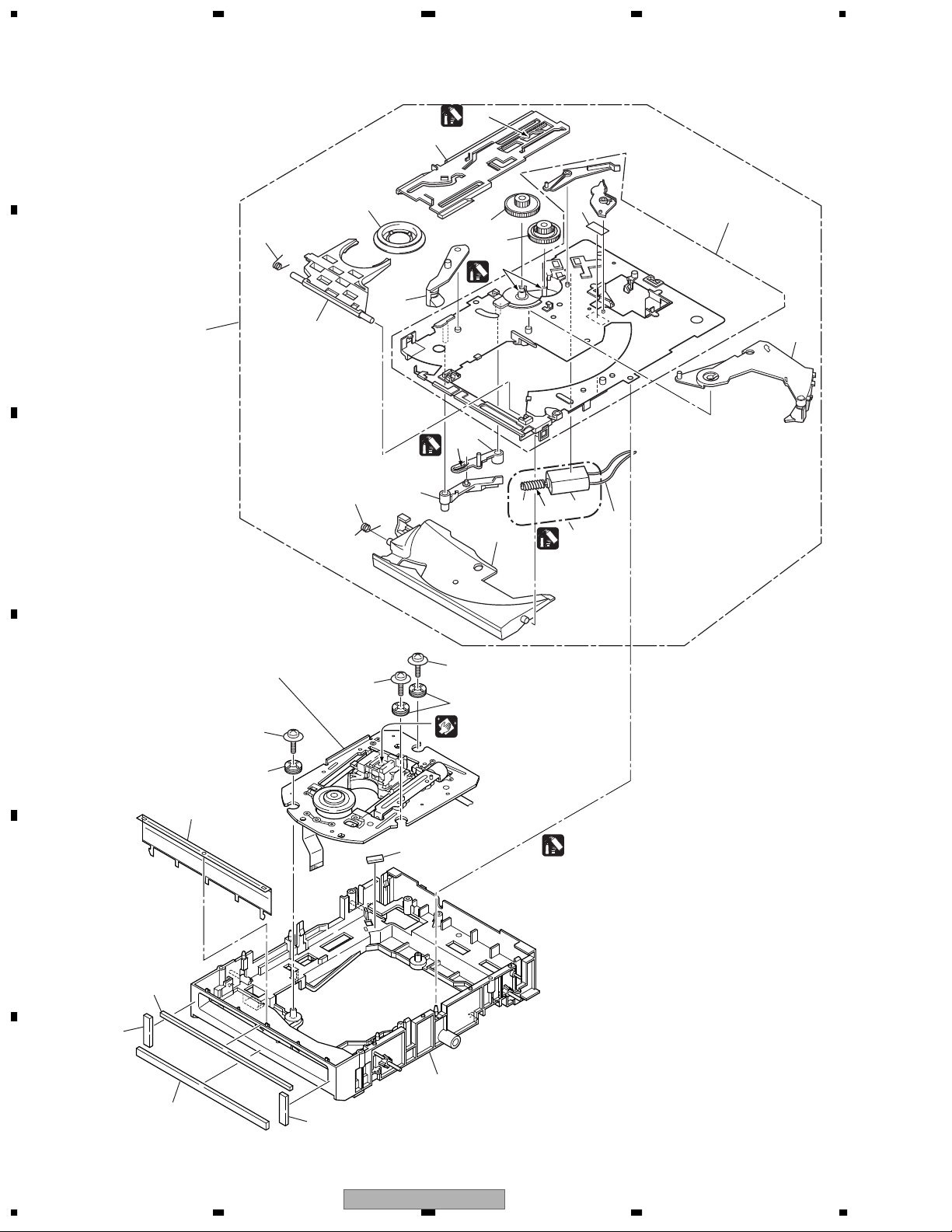
2.4 SLOT-IN MECHANISM SECTION
A
7
17
3
B
18
C
10
6
4
8
3
*
5
15
14
3
*
9
2
*
13
16
1
3
*
2
29
11
12
Refer to " 2.5 TRAVERSE MECHANISM ASSY-S ".
D
27
E
22
21
26
25
19
26
28
26
25
Cleaning liquid (GEM1004)
Cleaning paper (GED-008)
*
*
20
Dyefree : GEM1036 (ZLX-ME413A)
2.
Grease: GYA1001 (ZLB-PN397B)
3.
F
12
1234
23
21
CDJ-1000MK2
Page 13
12
10
2
5
7
3
9
11
5
4
6
8
1
13
8
6
4
*
5
*
4
Grease: GYA1001 (ZLB-PN397B)
*
4.
Grease: GEM1007 (ZLB-PN948P)
*
5.
*
4
Cleaning liquid (GEM1004)
Cleaning paper (GED-008)
5678
SLOT-IN MECHANISM SECTION Parts List
Mark
No. Description Part No.
NSP 1 DC Motor DXM1093
2 Connector Assy PF02PY-B32
3 Clamp Spring DBH1374
4 Guide Spring DBH1375
5 SW Lever Spacer (PET) DEC2420
Mark
No. Description Part No.
16 Disc Guide DNK3914
17 Clamper D4 Assy DXA1881
NSP 18 Slot-in Mechanism G5 Assy DXA1906
19 Traverse Mechanism Assy-S DXX2502
20 Float Base (G5) Assy DXB1748
A
6 Loading Lever DNK3406
7 Main Cam DNK3407
8 Lever B DNK3558
9 Lever A DNK3564
10 Clamp Arm DNK3576
11 Loading Base Assy-S DEA1022
12 Eject Lever DNK3684
NSP 13 Worm Gear DNK3910
14 Loading Gear DNK3911
15 Drive Gear DNK3912
TRAVERSE MECHANISM ASSY-S
21 Vessel Cushion C DEC2457
22 Vessel Cushion A DEC2455
23 Vessel Cushion B DEC2456
24 • • • • •
25 Float Rubber D3 DEB1404
26 Float Fastener DBA1139
27 Front Sheet DED1132
28 Spacer POR (T3) DEB1566
29 Loading Motor Assy-S DEA1008
B
C
TRAVERSE MECHANISM ASSY-S Parts List
No. Description Part No.
Mark
NSP 1 Spindle Motor DXM1138
NSP 2 Stepping Motor DXM1142
NSP 3 Pickup Assy VWY1069
NSP 4 Adjust Screw DBA1119
NSP 5 Precision Screw DBA1124
NSP 6 Skew Spring DBH1437
56
Mark No. Description Part No.
NSP 7 Joint Spring DBK1188
NSP 8 Guide Shaft DLA1840
NSP 9 Slider G4 DNK3733
NSP 10 Mechanism Frame G5 DNK3776
NSP 11 Joint DNK3777
12 Screw BPZ20P080FMC
13 Screw BPZ26P080FMC
CDJ-1000MK2
D
E
F
7
8
13
Page 14
1234
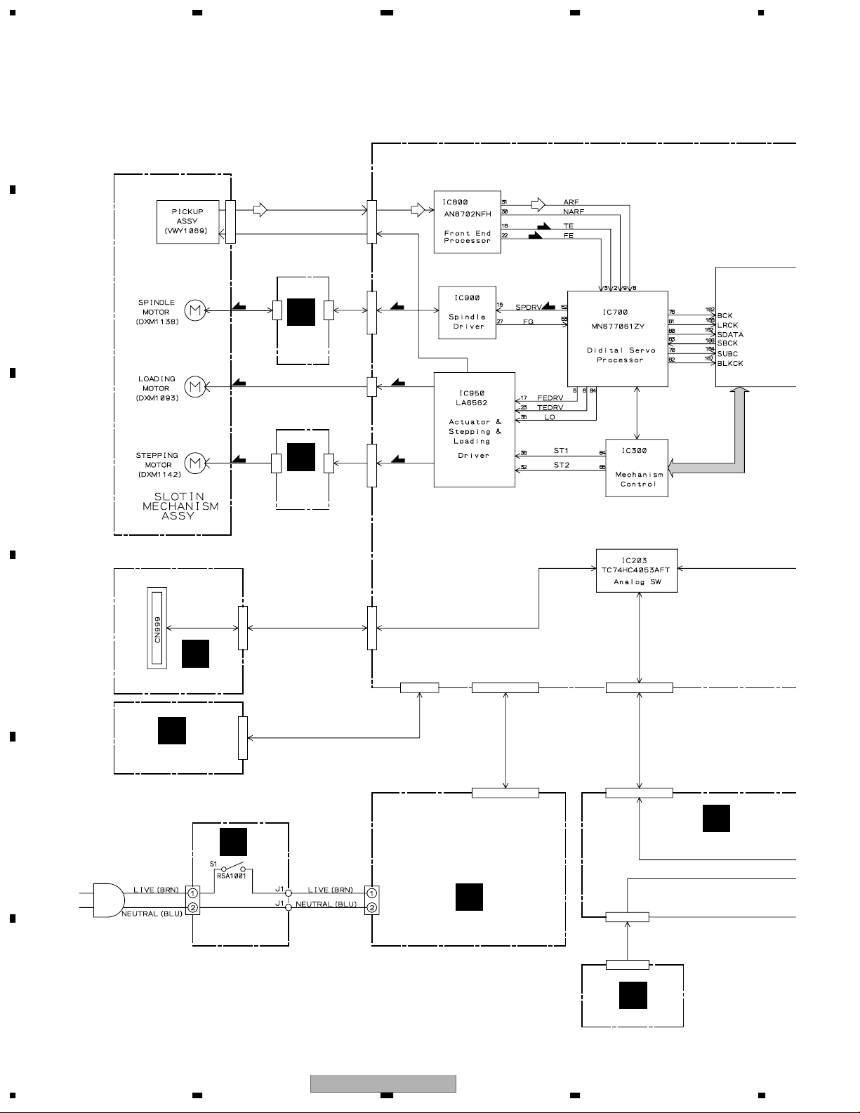
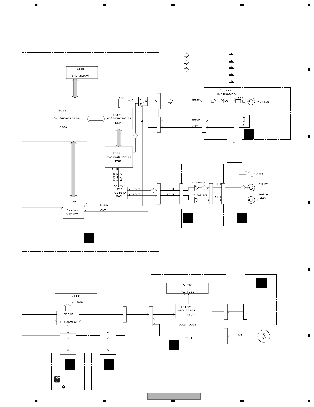
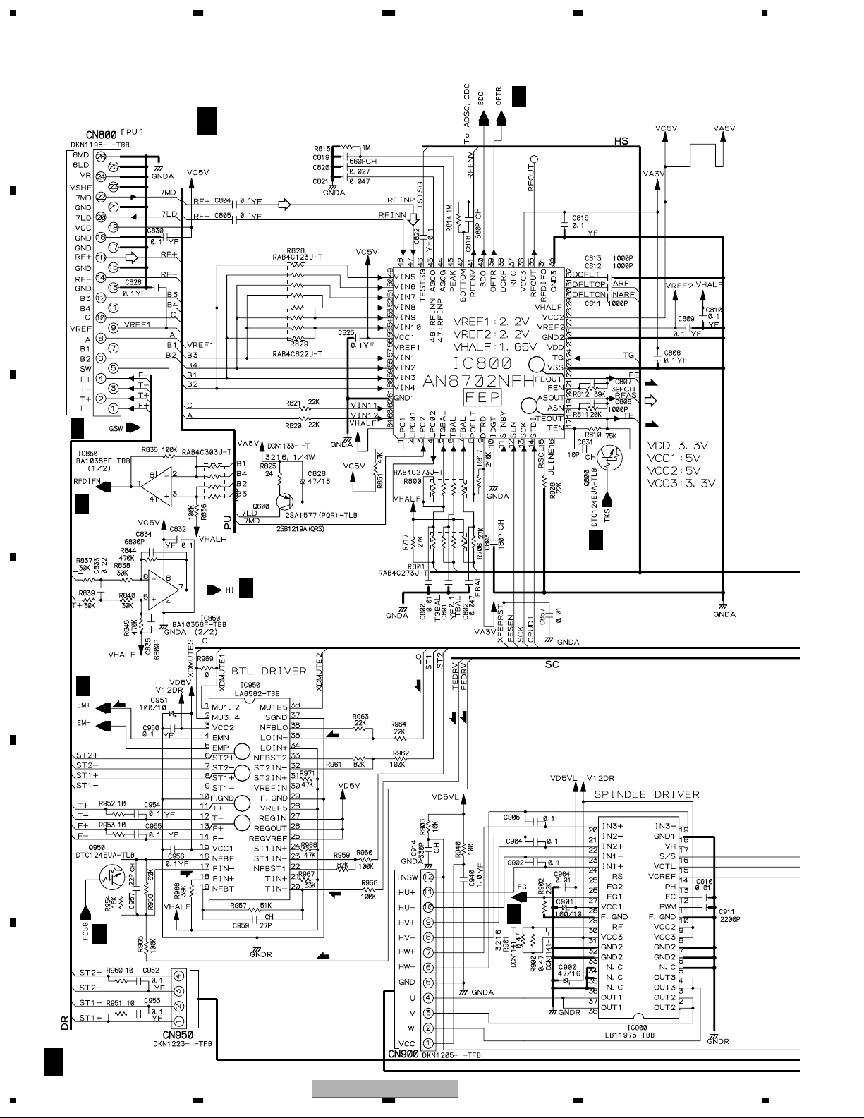
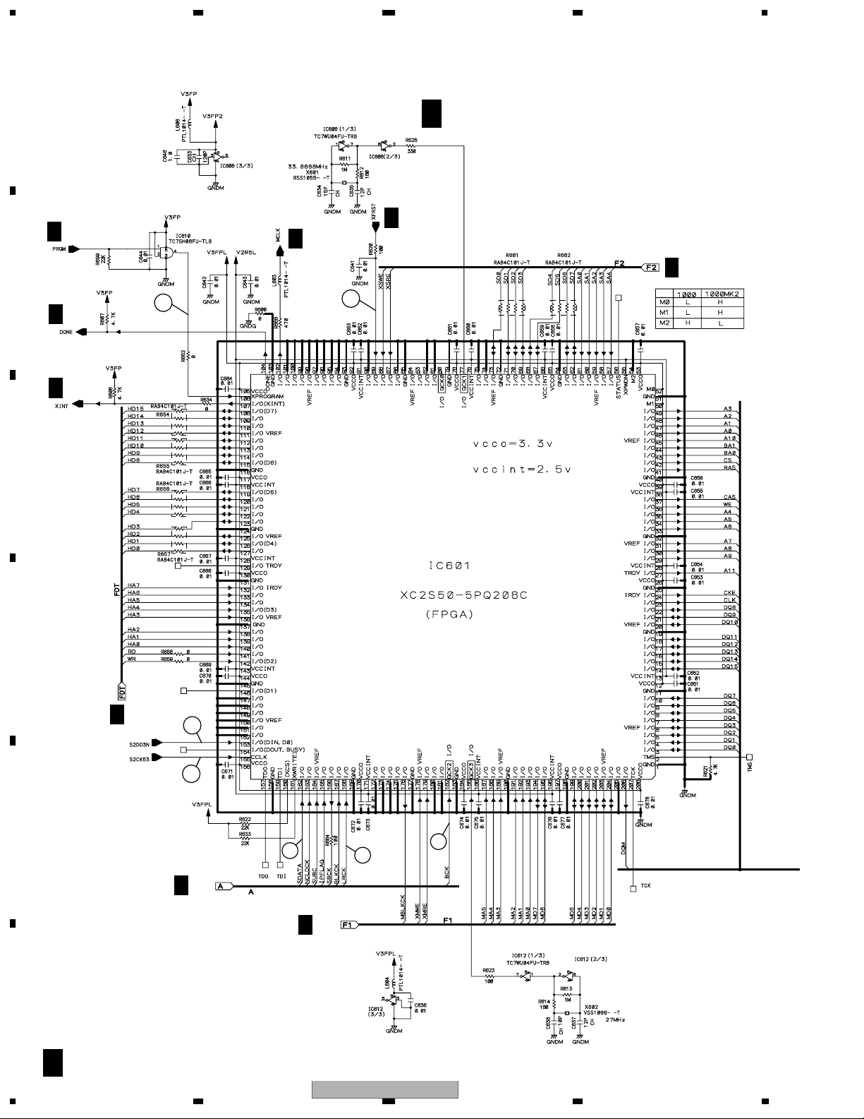
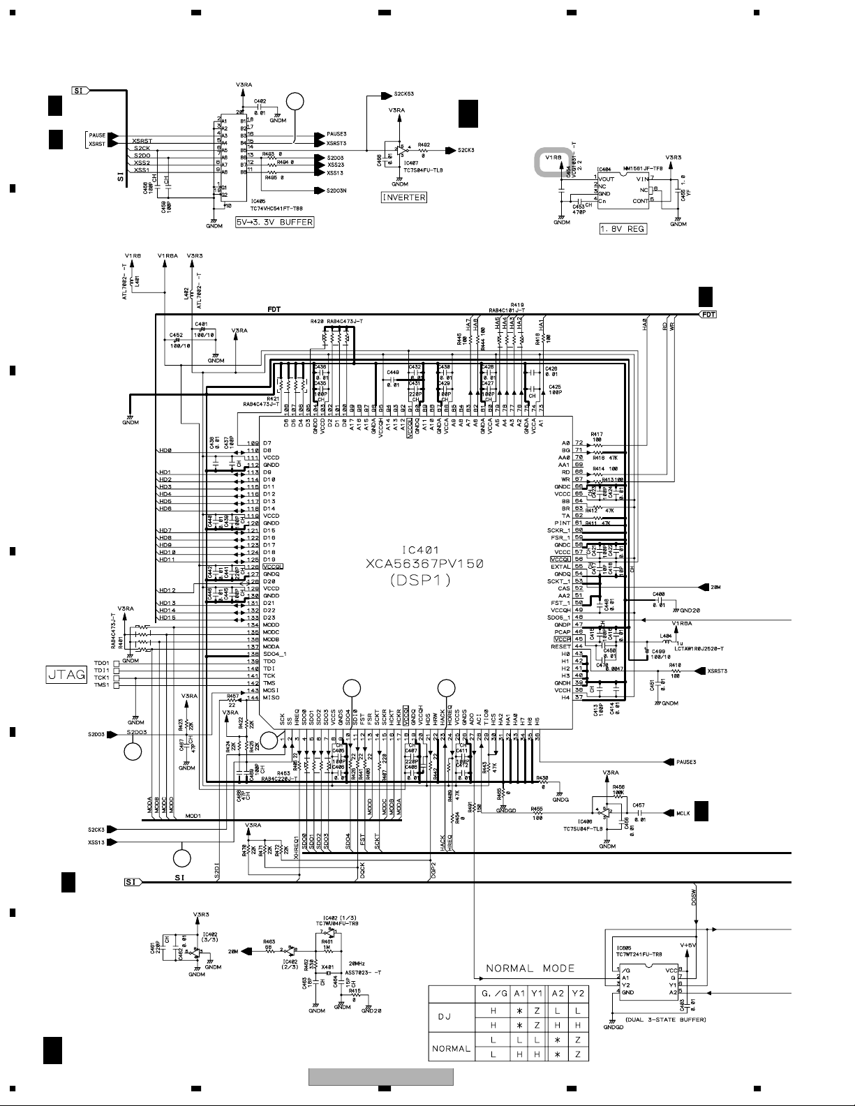
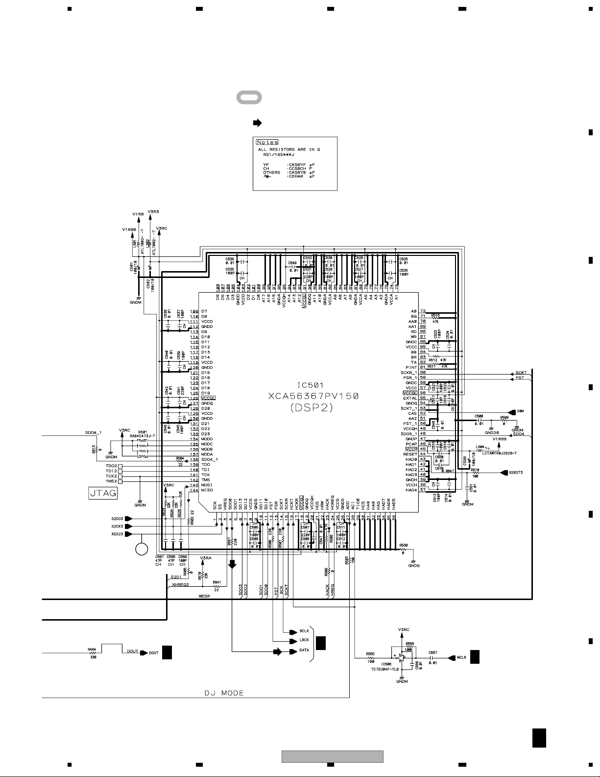
3. BLOCK DIAGRAM AND SCHEMATIC DIAGRAM
3.1 BLOCK DIAGRAM
A
CN801
B
(RF)
CN911
(SM)
CN912
B
CN800
#
CN900
47
(RF)
LB11975
(RF)
(FS)
(TS)
(SM)(SM)
SPCN
ASSY
CN302
C
(LM)
CN914CN913
(CM)
C
CN950
(LM)
(CM)
PD3446AB
STCN
ASSY
CN202CN99
D
MMC CARD
CONNECTOR
F
MMCB ASSY
CN1501
CN102
CN101
CN203
D
FLRB ASSY
CN201 CN1101
E
Q
AN1
PSWB ASSY
F
CN101
P
SW POWER SUPPLY ASSY
J1701
J1701
K
RSWB ASSY
J
MFLB ASSY
14
1234
CDJ-1000MK2
Page 15
5678
A
SIGNAL ROUTE
K4S641632F-TC75
IC605
TC7WT241FU
(D)
(D)
(D)
: DIGITAL SIGNAL
(PB)
: PB SIGNAL
(RF)
: RF SIGNAL
CN12
11
CN13
2
4
CN1801
(D)(D)
CN1802
2
4
(FS)
: FOCUS SERVO LOOP LINE
(TS)
: TRACKING SERVO LOOP LINE
(SM)
: SPINDLE MOTOR ROUTE
(CM)
: CARRIAGE MOTOR ROUTE
(LM)
: LOADING MOTOR ROUTE
JA1801
Digital Out
(D)
S1801
Digital Out Mode SW
DOUT ASSY
J1801
I
2
B
DJ/ NORMAL
PD3445A8
DEL1051
PE5387A
9
MAIN ASSY
A
J1101 J1103
CN1102
(PB)
J1202
5
6
7
CN11
4
1
4
1
(PB)
CN1901 CN1902
DABB
G
ASSY
DEL1050
161
CN1602
CN1201
6
CN1903
1
2
1
2
CN1904
(PB)
H
1
2
JA1901
Control Jack
BKB1017
JACB
ASSY
O
JOGB ASSY
CN1601
C
D
E
CN1401 CN1301
L
SLDB ASSYMKSWB ASSY
TEMPO
ZERO ADJ.
VR1402
56
JFLB ASSY
N
CDJ-1000MK2
SHEET SW
DSX1060
F
7
8
15
Page 16
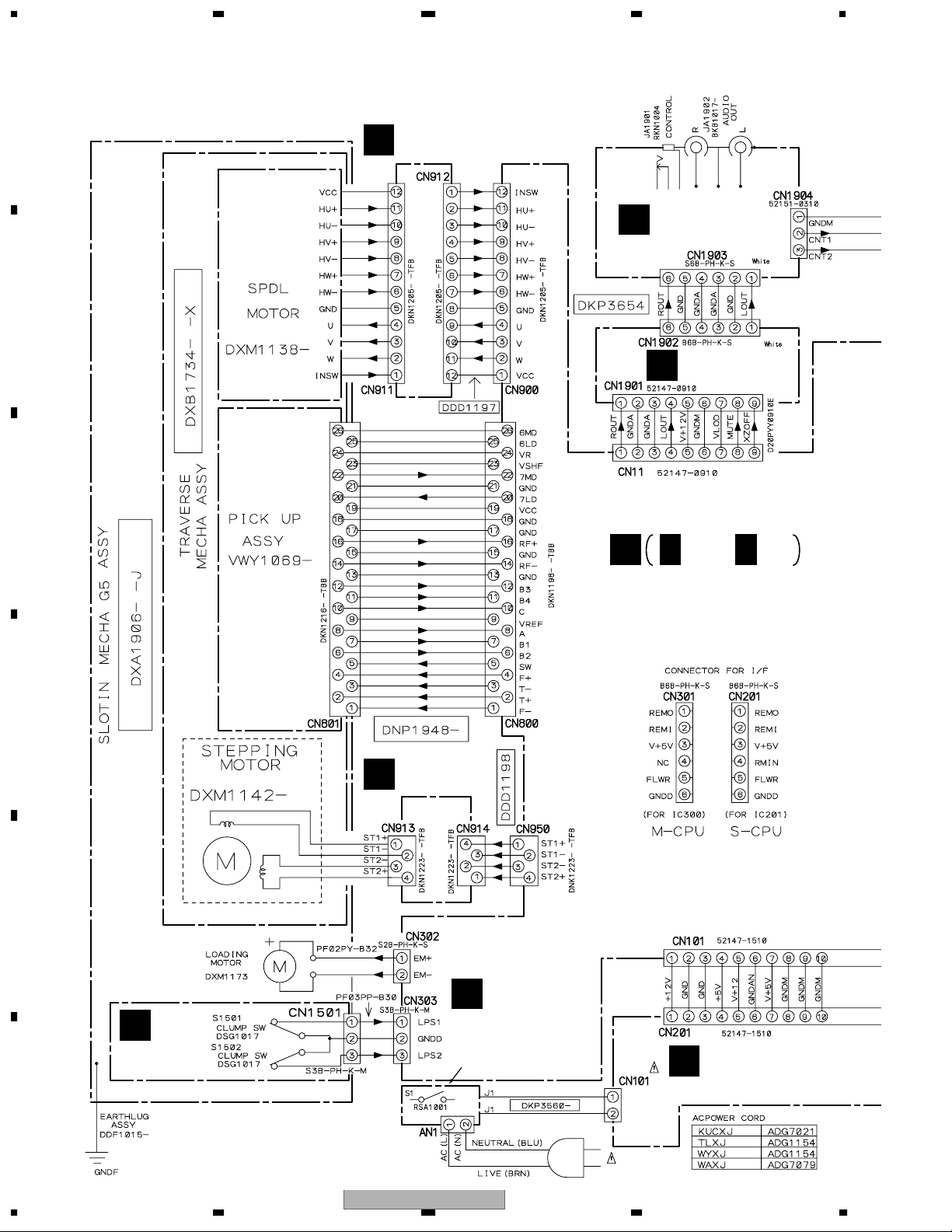
1234
3.2 OVERALL WIRING DIAGRAM
A
B
SPCN ASSY
B
(DWX2170)
JACB ASSY
H
(DWX2306)
G
DABB ASSY
(DWX2305)
C
A
A 1/4 - A 4/4
MAIN ASSY
(DWX2303)
D
STCN ASSY
C
(DWX2171)
E
Q
E
SLMB ASSY
(DWS1309)
F
AN1
KUCXJ: AKP7032
TLXJ, WYXJ: BKP1046
16
1234
CDJ-1000MK2
PSWB ASSY
(KUCXJ : DWS1312)
(TLXJ, WYXJ
: DWS1311)
SW POWER
P
SUPPLY ASSY
(DWR1370)
Page 17
5678
Note : When ordering service parts, be sure to refer to "EXPLODED VIEWS and PARTS LIST" or "PCB PARTS LIST".
DOUT ASSY
I
(DWX2307)
MMCB ASSY
F
(DWX2304)
KSWB ASSY
L
(DWS1324)
M
SLDB ASSY
(DWS1325)
A
B
C
FLRB ASSY
D
(DWX2308)
J
MFLB ASSY
(DWG1567)
J 1/2, J 2/2
JFLB ASSY
N
(DWG1568)
RSWB ASSY
K
(DWS1310)
JOGB ASSY
O
(DWG1569)
D
E
56
CDJ-1000MK2
F
7
8
17
Page 18
1234
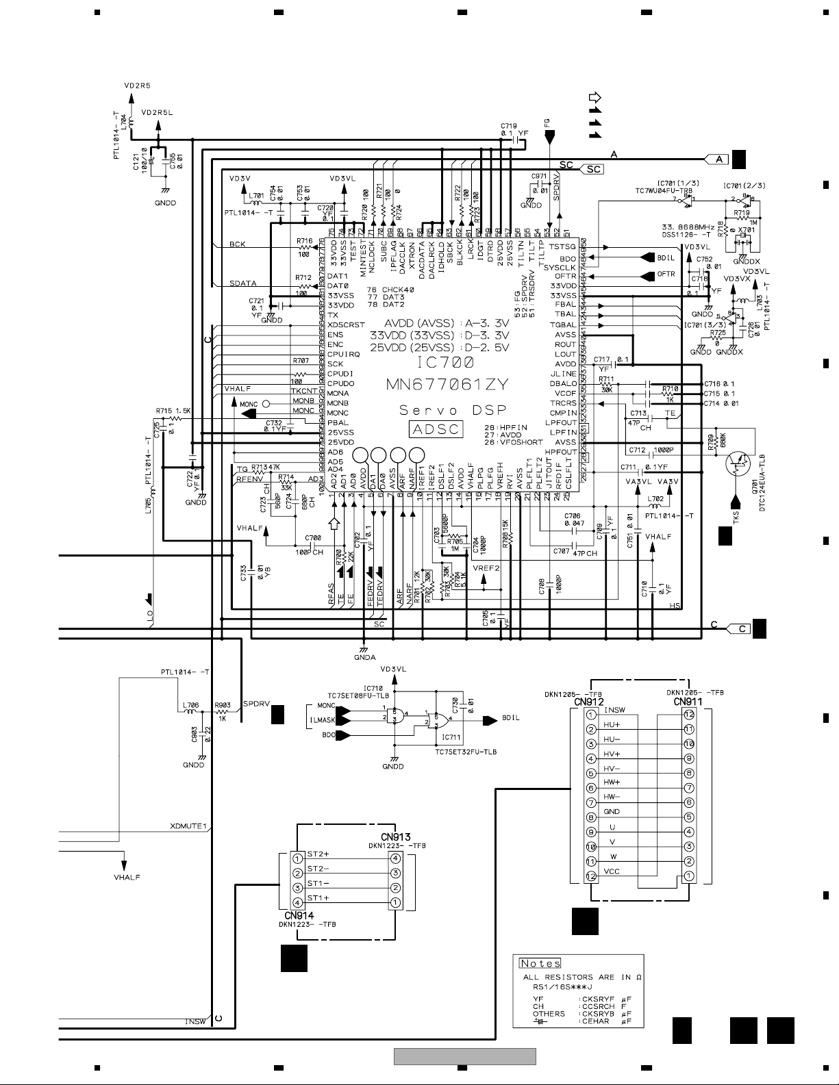
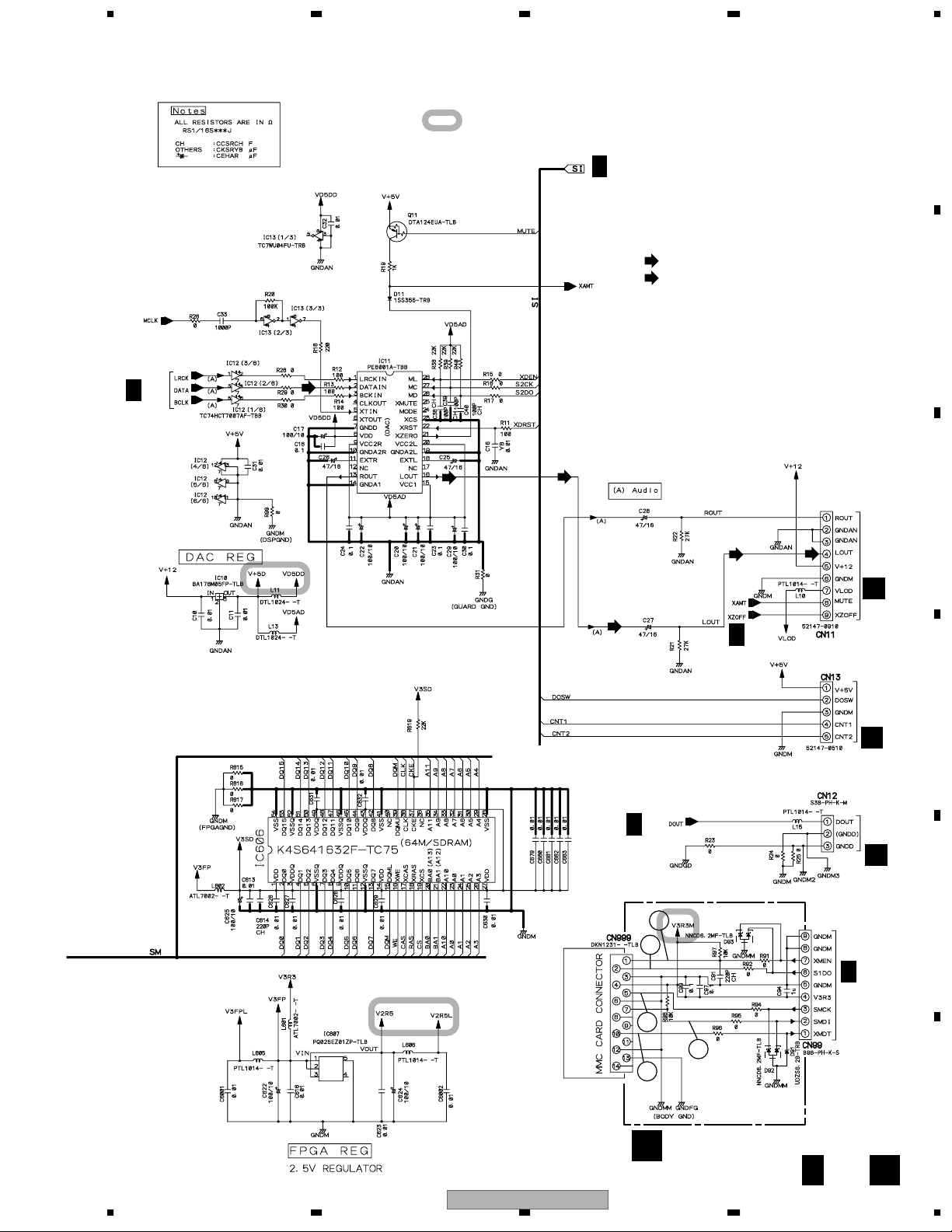
3.3 MAIN (1/4) and SPCN ASSYS
A
A 1/4
B
MAIN ASSY (DWX2303)
To PICKUP ASSY CN801
A 2/4
6
4
(FS)
(TS)
A 2/4
C
A 2/4
A 2/4
A 2/4
D
A 2/4
E
(L)
(L)
13
12
5
7
(FS)
(TS)
(L)
(FS)
(TS)
A 2/4
A 2/4
(FS)
F
A 1/4
18
1234
CDJ-1000MK2
Page 19
5678
: RF SIGNAL ROUTE
(L)
: LOADING MOTOR SIGNAL ROUTE
(FS)
: FOCUS SERVO SIGNAL ROUTE
(TS)
: TRACKING SERVO SIGNAL ROUTE
A
A 2/4, 3/4
B
19181011
C
A 2/4
(TS)
(FS)
(TS)
(L)
(FS)
A 2/4
D
A 2/4
To
SPINDLE
STCN ASSY
C
(DWX2171)
To
STEPPING
MOTOR
SPCN ASSY
B
(DWX2170)
MOTOR
(CN2220)
E
F
56
CDJ-1000MK2
A 1/4
7
B C
19
8
Page 20
1234
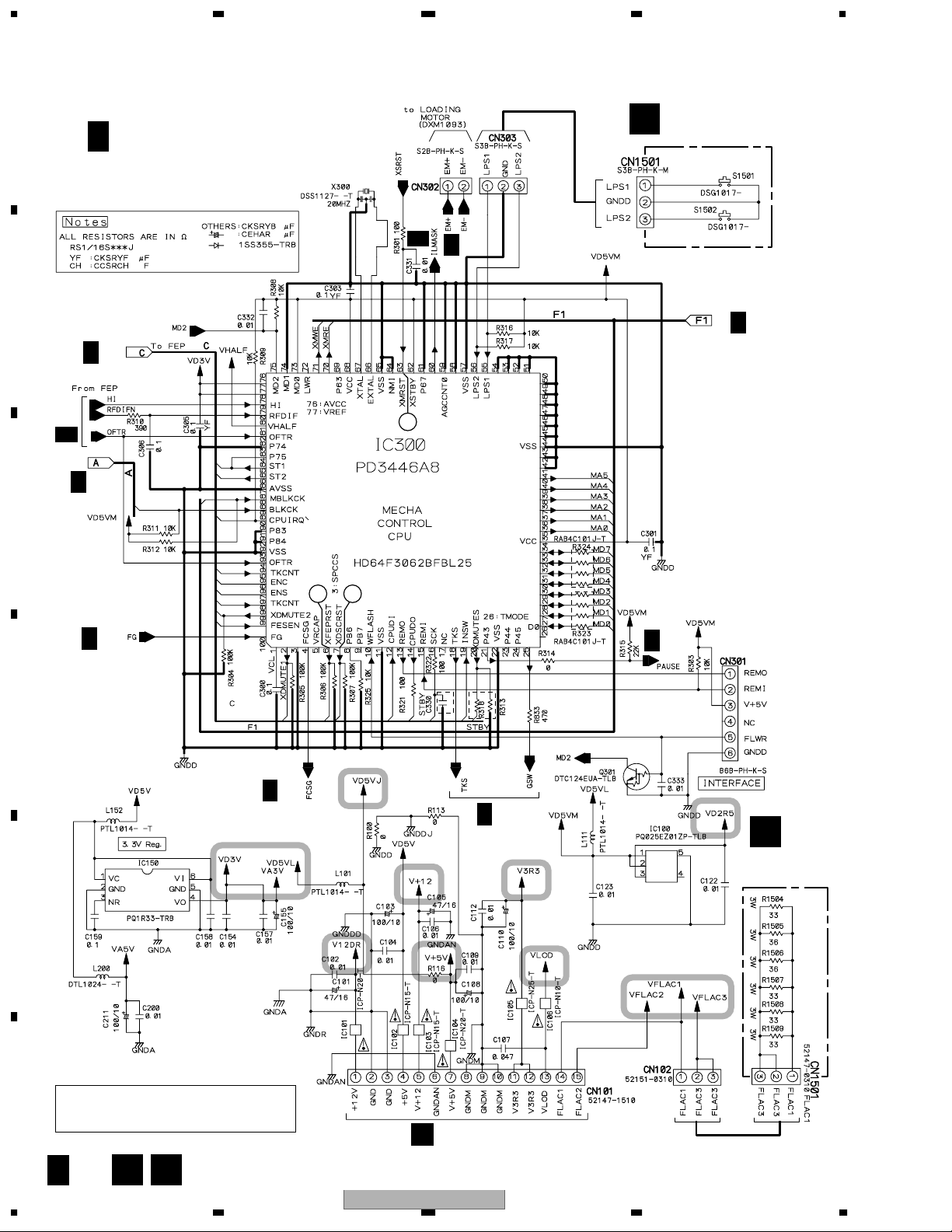
3.4 MAIN (2/4), FLRB and SLMB ASSYS
A
A 2/4
B
MAIN ASSY (DWX2303)
A 1/4
A 1/4
SLMB ASSY
E
(DWS1309)
CLAMP
CLAMP
A 3/4
A 1/4
A 1/4
36
A 1/4
C
4335
A 1/4
D
A 4/4
A 1/4
A 1/4
D
FLRB ASSY
(DWX2308)
E
F
CAUTION : FOR CONTINUED PROTECTION AGAINST
RISK OF FIRE, REPLACE ONLY WITH
SAME TYPE NO. ICP-N20, MFD BY ROHM
CO., LTD. FOR IC101 AND IC104.
A 2/4
20
E D
1234
CN201
P
CDJ-1000MK2
Page 21
5678
A 3/4,4/4
: The power supply is shown with the marked box.
A 3/4
26
A 3/4
1
A
B
C
A 3/4
21
A 4/4
3030
A 3/4
A 3/4
2 34
D
F
CN99
E
CN1101
J 1/2
CAUTION : FOR CONTINUED PROTECTION AGAINST
RISK OF FIRE, REPLACE ONLY WITH
SAME TYPE NO. ICP-N15, MFD BY ROHM
CO., LTD. FOR IC102 AND IC103.
56
CAUTION : FOR CONTINUED PROTECTION AGAINST
RISK OF FIRE, REPLACE ONLY WITH
SAME TYPE NO. ICP-N25, MFD BY ROHM
CO., LTD. FOR IC105.
CDJ-1000MK2
CAUTION : FOR CONTINUED PROTECTION AGAINST
RISK OF FIRE, REPLACE ONLY WITH
SAME TYPE NO. ICP-N10, MFD BY ROHM
CO., LTD. FOR IC106.
7
F
A 2/4
21
8
Page 22
1234
3.5 MAIN (3/4) and MMCB ASSYS
A
A 3/4
MAIN ASSY (DWX2303)
A 2/4
B
20
A 3/4,4/4
A 2/4
3
A 2/4
A 2/4
A 2/4
C
D
A 4/4
E
25
24
14
16
15
A 1/4
A 2/4
F
A 3/4
22
1234
CDJ-1000MK2
Page 23
5678
A 4/4
: The power supply is shown with the marked box.
A
A 2/4,4/4
: PB AUDIO SIGNAL ROUTE
(D)
: DIGITAL DATA SIGNAL ROUTE
B
(D)
C
A 4/4
41
40
A 2/4
A 2/4
CN202
CN1901
G
CN1802
I
CN1801
I
D
E
56
CDJ-1000MK2
39
38
MMCB ASSY
F
(DWX2304)
7
42
A 3/4
8
F
F
23
Page 24
1234
3.6 MAIN ASSY (4/4)
A
B
C
A 2/4,3/4
A 2/4
22
A 4/4
MAIN ASSY (DWX2303)
A 3/4
D
2931
33
E
28
32
A 3/4
A 2/4,3/4
F
A 4/4
24
1234
CDJ-1000MK2
Page 25
5678
A
: The power supply is shown with the marked box.
(D)
: DIGITAL DATA SIGNAL ROUTE
B
27
C
D
(D)
E
(D)
A 3/4
A 3/4
56
CDJ-1000MK2
A 3/4
F
A 4/4
7
8
25
Page 26
1234
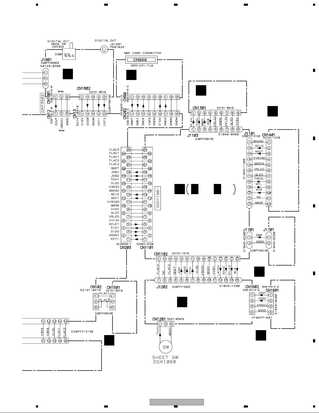
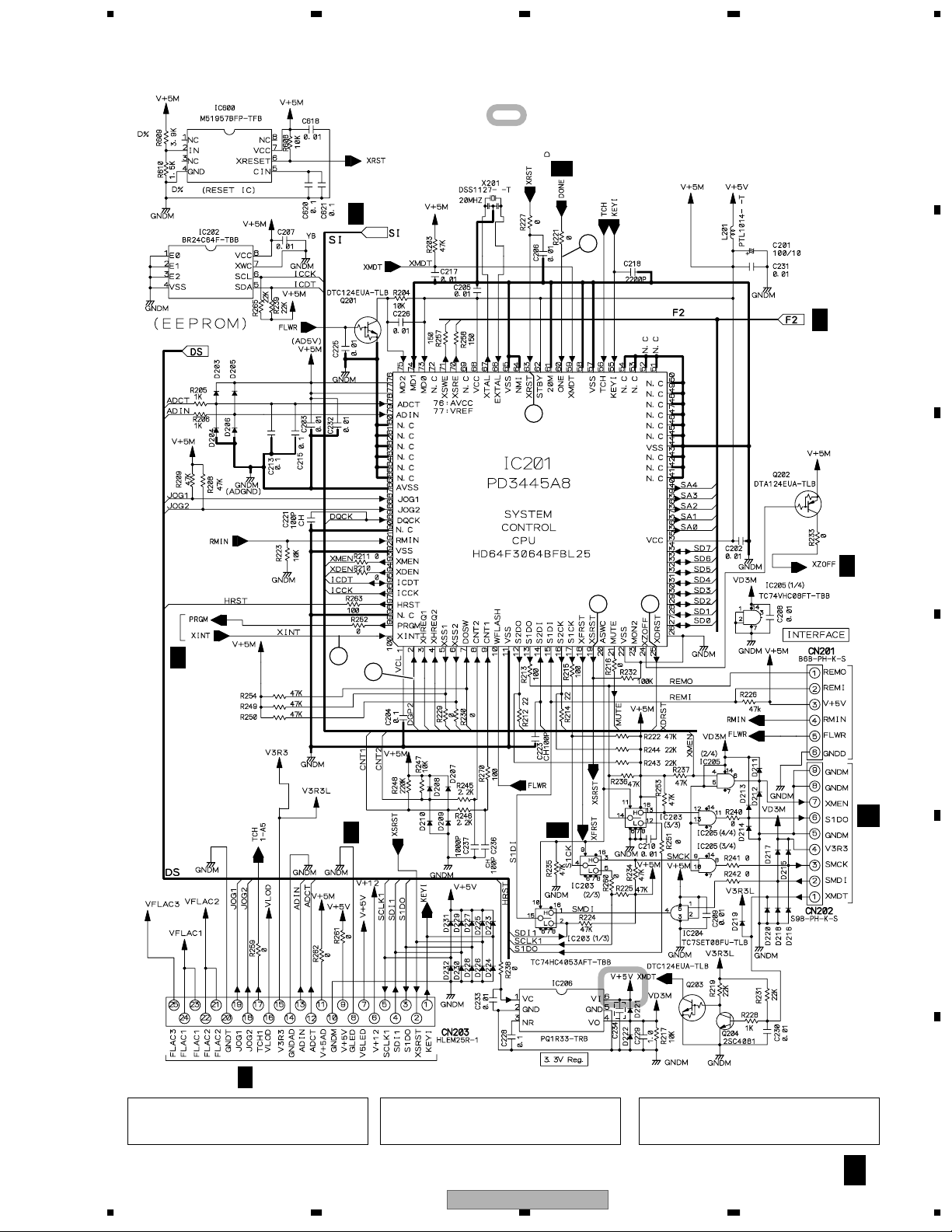
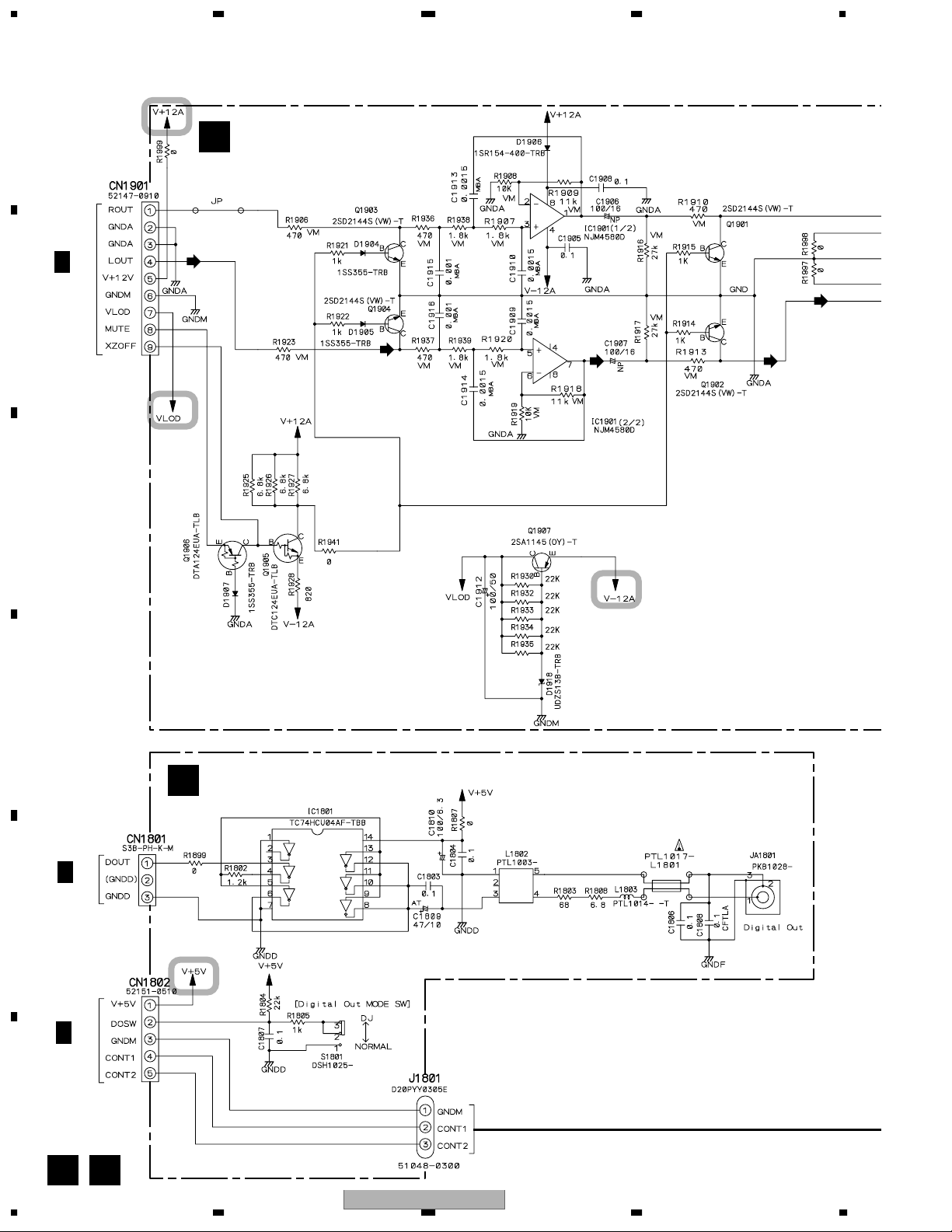
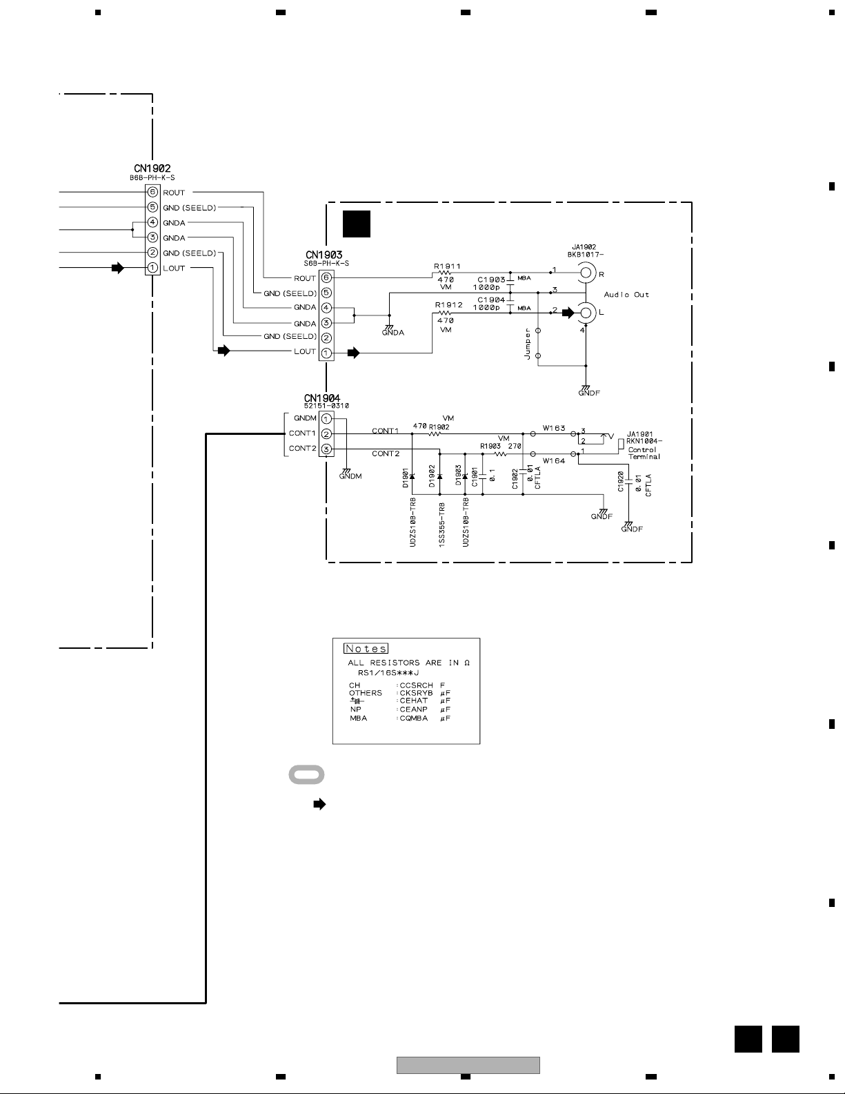
3.7 DABB, JACB and DOUT ASSYS
A
DABB ASSY (DWX2305)
G
A 3/4
CN11
B
C
D
DOUT ASSY (DWX2307)
I
A 3/4
CN12
E
F
A 3/4
CN13
G I
26
1234
CDJ-1000MK2
Page 27
5678
A
JACB ASSY (DWX2306)
H
B
: The power supply is shown with the marked box.
: PB AUDIO SIGNAL ROUTE
C
D
E
56
CDJ-1000MK2
F
G H
7
8
27
Page 28
1234
3.8 MFLB (1/2) and RSWB ASSYS
A
J 1/2
B
MFLB ASSY (DGW1567)
: The power supply is shown with the marked box.
J 2/2
37
C
A 2/4
CN203
D
E
F
J 1/2
28
CN1401
M
CDJ-1000MK2
1234
N
J1202
Page 29
5678
SWITCHES
MFLB ASSY
S1101 : A
S1102 : B
S1103 : C
S1104 : DISPLAY
TEXT/WAVE
S1105 : TIME MODE
S1106 : 0 (EJECT)
S1107 : SELECT
VINYL – CDJ
S1109 : 2 CALL
S1110 : CALL 3
S1111 : MEMORY
S1112 : DELETE
S1113 : IN/REALTIME CUE
S1114 : LOOP OUT
S1115 : RELOOP/EXIT
S1116 : 2 WAVE
S1117 : WAVE 3
S1118 : EJECT LOCK
S1119 : SELECT
RSWB ASSY
S1701 : FWD – REV
A
B
C
10k-B
10k-B
J 2/2
CN1301
L
56
CDJ-1000MK2
D
E
K
RSWB ASSY
(DWS1310)
J 1/2
7
K
8
F
29
Page 30

1234
3.9 MFLB (2/2) ASSY
A
J 2/2
MFLB ASSY (DGW1567)
J 1/2
J 1/2
B
C
D
J 1/2
E
J 1/2
F
J 2/2
30
1234
CDJ-1000MK2
Page 31

5678
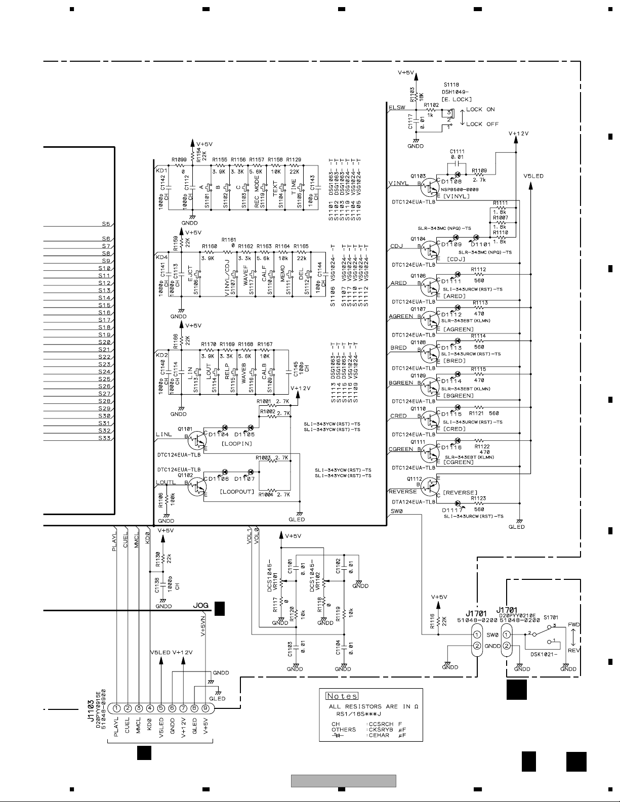
3.10 KSWB and SLDB ASSYS
J 1/2
J1103
KSWB ASSY (DWS1324)
L
A
B
J 1/2
J1101
SWITCHES
KSWB ASSY
S1301 : CUE
S1302 : 6
S1303 : 4
S1304 : ¢
S1305 : 1
S1306 : ¡
SLDB ASSY (DWS1325)
M
SWITCHES
SLDB ASSY
S1401 : TEMPO RESET
S1402 : MASTER TEMPO
S1403 : TEMPO RANGE
TEMPO ZERO
POINT ADJ.
C
D
E
: The power supply is shown with the marked box.
CDJ-1000MK2
56
F
L M
7
8
31
Page 32

1234
3.11 JFLB and JOGB ASSYS
A
JFLB ASSY (DWG1568)
N
B
C
D
E
CN1102
J 1/2
F
N
32
1234
CDJ-1000MK2
Page 33

5678
A
B
IC1201
UPD16306B
DRIVER IC
C
D
To SHEET SW
E
JOGB ASSY (DWG1569)
O
: The power supply is shown with the marked box.
56
CDJ-1000MK2
F
N O
7
8
33
Page 34

1234
3.12 SW POWER SUPPLY and PSWB ASSYS
A
+12V
5
+5V Servo3GND7+5V
GND
6
4
3.3V123.3V
11
+12V Servo
GND
2
A 2/4
CN101
GND9GND
8
GND
10
-38.5V
13
FLAC 115FLAC 2
14
CN201
C212 R219
C209
L206
B
D206
R206
ZD203
L207
R201
C201
C
R224
C217
D201
D202
R212
PC101
R218
C216
D205
R202
R211
IC202
C207
C202
R210
C203
R203
C210
IC201
R205
C214
Q201
R217 R215
R208
VR201
C215
C213
R214
Q202
C204
R209
R222
R306
ZD201
R301
R307
D302
D310
D301
C306
L301
D308
R302
D303
C307 R310
D305
R303
R305
C301
Q301
Q302
VR301
C302
D309
D304
C303
FOR CONTINUED PROTECTION AGAINST RISK OF FIRE.
REPLACE WITH SAME TYPE AND RATINGS ONLY.
S3
T101
P1 S4
D
PC
D101
E
C102
P2
L103 L202
C107
R107
D104
Q101
L105
R117
R104
C105
R118R119
C104
L101 L102
R108
TH101
PC
S2
L104
R115 R220R122
D103 D204
R120
R101R102
C103
B2 S5
C115
R113
3
76
IC101
8
R109
S1
4
Q102
ZD101
C113
152
C112
R112
R114
C109
C108
R121
S8
C111
PC101
S7
B1
CAUTION -
• NOTE FOR FUSE REPLACEMENT
AC IN
C114
LIVE
NEUTRAL
AN1 ;
KUCXJ : AKP7032
TLXJ, WYXJ : BKP1046
(TLXJ, WYXJ : DWS1311)
PSWB ASSY (KUCXJ : DWS1312)
C101
SW POWER SUPPLY ASSY (DWR1370)
F
P
F101
1 1
CN101
2
Q
P Q P Q
34
1234
CDJ-1000MK2
Page 35

1
2
1
2
IC201- 63pin (XRST)
V: 2V/div. H: 20mS/div.
IC201- 19pin (XSRST)
V: 2V/div. H: 20mS/div.
Mode: Power ON
1
3
1
3
IC201- 63pin (XRST)
V: 2V/div. H: 50mS/div.
IC601- 89pin (XFRST)
V: 2V/div. H: 50mS/div.
4
5
4
5
IC800- 18pin (TE)
V: 1V/div. H: 200µS/div.
IC950- 11pin (T+)
V: 500mV/div. H: 200µS/div.
6
7
6
7
IC800- 22pin (FE)
V: 1V/div. H: 50mS/div.
IC950- 13pin (F+)
V: 1V/div. H: 50mS/div.
4
4
IC800- 18pin (TE)
V: 500mV/div. H: 500µS/div.
Mode: 1track Jump
6
6
IC800- 22pin (FE)
V: 200mV/div. H: 500µS/div.
10
10
IC700- 6pin (TEDRV)
V: 200mV/div. H: 5µS/div.
11
11
IC700- 5pin (FEDRV)
V: 100mV/div. H: 20mS/div.
12
13
12
13
IC950- 8pin (ST1+)
V: 5V/div. H: 20mS/div.
IC950- 6pin (ST2+)
V: 5V/div. H: 20mS/div.
Mode: Search
14
14
IC601- 162pin (SDATA)
V: 2V/div. H: 1µS/div.
15
15
IC601- 182pin (BCK)
V: 2V/div. H: 500nS/div.
16
16
IC601- 168pin (LRCK)
V: 2V/div. H: 5µS/div.
17
17
IC604- 3pin (VCOOUT)
V: 2V/div. H: 20nS/div.
Mode: Play
18
19
18
19
IC700- 8pin (ARF)
V: 200mV/div. H: 50nS/div.
IC700- 9pin (NARF)
V: 200mV/div. H: 50nS/div.
Mode: Power ON
Mode: Focus Up/Down
Mode: Search
Mode: Play
Mode: Play
Mode: Play
Mode: Play
Mode: Play
Mode: 3100rpm/ Inside Play
Mode: Focus
A 2/4
MAIN ASSY
A 2/4, 3/4
MAIN ASSY
A 1/4
MAIN ASSY
A 3/4
MAIN ASSY
A 1/4
MAIN ASSY
A 1/4
MAIN ASSY
A 1/4
MAIN ASSY
A 3/4
MAIN ASSY
A 1/4
MAIN ASSY
A 1/4
MAIN ASSY
A 1/4
MAIN ASSY
A 1/4
MAIN ASSY
A 3/4
MAIN ASSY
A 3/4
MAIN ASSY
WAVEFORMS
5678
A
B
C
D
E
56
CDJ-1000MK2
F
7
8
35
Page 36

1234
MAIN ASSY
A
A
IC201 - pin 63 [XRST]
1
A 2/4
A 3/4
A 2/4
1
20
B
21
A 3/4
A 2/4
C
20
V: 5V/div. H: 1msec/div.
IC601 - pin 106 [PRGM]
20
V: 5V/div. H: 1msec/div.
IC201 - pin 100 [XINT]
21
V: 5V/div. H: 1msec/div.
IC601 - pin 106 [PRGM]
20
V: 2V/div. H: 5µsec/div.
IC201 - pin 100 [XINT]
21
V: 2V/div. H: 5µsec/div.
MFLB ASSY
J
IC201 - pin 100 [XINT]
21
A 2/4
A 3/4
A 3/4
A 2/4 A 2/4
21
24
25
26
A 2/4
A 3/4
A 4/4
26
3
V: 5V/div. H: 100msec/div.
IC601 - pin 155 [S2CK53]
24
V: 5V/div. H: 100msec/div.
IC601 - pin 153 [S2D03N]
25
V: 5V/div. H: 100msec/div.
IC201 - pin 60 [D0NE]
26
V: 5V/div. H: 100msec/div.
IC201 - pin 60 [D0NE]
26
V: 5V/div. H: 1msec/div.
IC601 - pin 89 [XFRST]
3
V: 5V/div. H: 1msec/div.
IC405 - pin 15 [XSRST3]
22
V: 5V/div. H: 1msec/div.
A 4/4
A 4/4
A 4/4
27
28
29
30
A 4/4
A 4/4
A 4/4
A 2/4
27
28
IC501 - pin 2 [XSS23]
27
V: 5V/div. H: 500µsec/div.
IC401 - pin 2 [XSS13]
28
V: 5V/div. H: 500µsec/div.
IC401 - pin 23 [HACK]
29
V: 5V/div. H: 500µsec/div.
IC201 - pin 2 [DGP2]
30
V: 5V/div. H: 500µsec/div.
Zoom-up
IC501 - pin 2 [XSS23]
27
V: 5V/div. H: 50msec/div.
IC401 - pin 2 [XSS13]
28
V: 5V/div. H: 50msec/div.
IC401 - pin 10 [SD04_1]
31
V: 5V/div. H: 50msec/div.
IC201 - pin 2 [DGP2]
30
V: 5V/div. H: 50msec/div.
A 2/4
A 3/4
1
3
A 2/4
1
IC201 - pin 63 [XRST]
1
V: 2V/div. H: 200msec/div.
IC601 - pin 89 [XFRST]
3
V: 2V/div. H: 200msec/div.
Reset timing
IC201 - pin 63 [XRST]
1
V: 2V/div. H: 200msec/div.
IC201 - pin 25 [XDRST]
34
V: 2V/div. H: 200msec/div.
Reset timing
21
IC601 - pin 106 [PRGM]
20
A 3/4
A 2/4
A 3/4
D
A 3/4
20
21
24
25
A 3/4
E
A 2/4
A 3/4
A 3/4
20
21
24
25
F
V: 5V/div. H: 100msec/div.
IC201 - pin 100 [XINT]
21
V: 5V/div. H: 100msec/div.
IC601 - pin 155 [S2CK53]
24
V: 5V/div. H: 100msec/div.
IC601 - pin 153 [S2D03N]
25
V: 5V/div. H: 100msec/div.
IC601 - pin 106 [PRGM]
20
V: 5V/div. H: 5µsec/div.
IC201 - pin 100 [XINT]
21
V: 5V/div. H: 5µsec/div.
IC601 - pin 155 [S2CK53]
24
V: 5V/div. H: 5µsec/div.
IC601 - pin 153 [S2D03N]
25
V: 5V/div. H: 5µsec/div.
22
A 2/4
A 3/4
A 4/4
A 4/4
26
3
22
27
IC201 - pin 60 [D0NE]
26
V: 5V/div. H: 100msec/div.
IC601 - pin 89 [XFRST]
3
V: 5V/div. H: 100msec/div.
IC405 - pin 15 [XSRST3]
22
V: 5V/div. H: 100msec/div.
IC501 - pin 2 [XSS23]
27
V: 5V/div. H: 100msec/div.
31
30
A 4/4
27
28
32
33
A 4/4
28
27
32
33
IC501 - pin 2 [XSS23]
27
V: 5V/div. H: 500µsec/div.
IC401 - pin 2 [XSS13]
28
V: 5V/div. H: 500µsec/div.
IC401 - pin 1 [S2CK3]
32
V: 5V/div. H: 500µsec/div.
IC401 - pin 143 [S2D03]
33
V: 5V/div. H: 500µsec/div.
Zoom-up
IC401 - pin 2 [XSS13]
28
V: 5V/div. H: 50msec/div.
IC501 - pin 2 [XSS23]
27
V: 5V/div. H: 50msec/div.
IC401 - pin 1 [S2CK3]
32
V: 5V/div. H: 50msec/div.
IC401 - pin 143 [S2D03]
33
V: 5V/div. H: 50msec/div.
34
A 2/4
1
34
35
A 2/4
A 2/4
J 1/2
A 4/4
1
Mecha. com.
36
FL com.
37
DSP
22
IC201 - pin 63 [XRST]
1
V: 5V/div. H: 500msec/div.
IC300 - pin 7 [XDSCRST]
43
V: 5V/div. H: 500msec/div.
IC300 - pin 6 [XFEPRST]
35
V: 5V/div. H: 500msec/div.
Reset timing
IC201 - pin 63 [XRST]
1
V: 5V/div. H: 200msec/div.
IC300 - pin 63 [XSRST]
36
V: 5V/div. H: 200msec/div.
IC1101 - pin 10 [XSRST]
37
V: 5V/div. H: 200msec/div.
IC405 - pin 15 [XSRST]
22
V: 5V/div. H: 200msec/div.
Reset timing
36
1234
CDJ-1000MK2
Page 37

A 3/4 A 3/4
A 3/4
38
CN999 - pin 10 [XMDT]
V: 5V/div. H: 200msec/div.
39
CN999 - pin 5 [SMCK]
V: 5V/div. H: 200msec/div.
40
CN999 - pin 2 [S1D0]
V: 5V/div. H: 200msec/div.
41
CN999 - pin 1 [XMEN]
V: 5V/div. H: 200msec/div.
A 3/4
38
CN999 - pin 10 [XMDT]
V: 5V/div. H: 200msec/div.
39
CN999 - pin 5 [SMCK]
V: 5V/div. H: 200msec/div.
40
CN999 - pin 2 [S1D0]
V: 5V/div. H: 200msec/div.
42
CN999 - pin 7 [SMDI]
V: 5V/div. H: 200msec/div.
39
CN999 - pin 5 [SMCK]
V: 5V/div. H: 1sec/div.
40
CN999 - pin 2 [S1D0]
V: 5V/div. H: 1sec/div.
42
CN999 - pin 7 [SMDI]
V: 5V/div. H: 1sec/div.
41
CN999 - pin 1 [XMEN]
V: 5V/div. H: 1sec/div.
39
CN999 - pin 5 [SMCK]
V: 5V/div. H: 20msec/div.
40
CN999 - pin 2 [S1D0]
V: 5V/div. H: 20msec/div.
42
CN999 - pin 7 [SMDI]
V: 5V/div. H: 20msec/div.
41
CN999 - pin 1 [XMEN]
V: 5V/div. H: 20msec/div.
A 3/4
39
CN999 - pin 5 [SMCK]
V: 5V/div. H: 20msec/div.
40
CN999 - pin 2 [S1D0]
V: 5V/div. H: 20msec/div.
42
CN999 - pin 7 [SMDI]
V: 5V/div. H: 20msec/div.
41
CN999 - pin 1 [XMEN]
V: 5V/div. H: 20msec/div.
38
39
40
41
39
40
42
41
38
39
40
42
39
40
42
41
39
40
42
41
MAIN ASSY
A
MMC Card IN 1 at LOOP memory and delete
MMC Card IN 2
HOT CUE REC
HOT CUE CALL
5678
A
B
C
D
E
F
56
CDJ-1000MK2
7
8
37
Page 38

1234
VOLTAGES
A
IC700 (MN677061ZY)
Pin No. Voltage (V)
1 2.1
2 1.4
3 1.6
4 3.3
5 1.6
6 1.6
70
8 1.6
9 1.6
10 1.5
11 1.5
12 1.6
13 1.5
B
C
D
E
F
14 3.3
15 1.7
16 2.2
17 0.2
18 2.1
19 1.4
20 0
21 1
22 1
23 2
24 1.6
25 1.1
26 1.1
27 3.3
28 1.1
29 1.1
30 0
31 1
32 1
33 1.6
34 1.6
35 1
36 1.2
37 1.6
38 3.3
39 0
40 1.6
41 0
42 1.6
43 0
44 1.8
45 0
46 3.3
47 0
48 1.6
49 0
50 0
51 1.7
52 1.9
53 1.5
54 1.1
55 1.1
56 1.1
57 0
58 2.4
59 0
60 0
61 1.6
62 0
63 0.3
64 0
65 0
66 0
67 0
68 1.6
69 0.2
70 0.1
71 3.2
72 0
73 0
74 0
75 3.3
76 1.7
77 0
78 0
79 1.7
80 1.6
81 0
82 3.3
83 84 4.9
85 4.8
86 4.9
87 3.2
88 4.9
89 4.8
90 0.7
Voltage measurement mode
DJ MODE: PLAY , VINAL , MMC IN , MASTER TEMPO: OFF , SRIDER: 0%, HOT CUE: OFF
A
1/4
MAIN ASSY
IC700 (MN677061ZY)
Pin No. Voltage (V)
91 0 to 3.2
92 0
93 0
94 1.6
95 0
96 2.4
97 1.7
98 1.7
99 1.6
100 2.3
IC701 (TC7WU04FU)
Pin No. Voltage (V)
1 1.7
2 1.7
3 3.3
4 0
5 0
6 1.7
7 1.6
8 3.3
IC710 (TC7SET08FU)
Pin No. Voltage (V)
1 0
2 0 to 4.9
3 0
4 0
5 3.3
IC711(TC7SET32FU)
Pin No. Voltage (V)
1 0
2 0
3 0
4 0
5 3.3
IC800 (AN8702NFH)
Pin No. Voltage (V)
1 4.9
2 2.2
3 0.2
4 3.2
5 1.7
6 1.7
7 1.7
8 3.9
9 3.3
10 0
11 4.9
12 4.9
13 4.9
14 4.9
15 1.2
16 1.7
17 1.8
18 1.4
19 1.7
20 2.2
21 1.7
22 1.6
23 0
24 1.6
25 3.3
26 0
27 2.1
28 4.9
29 1.7
30 2
31 2
32 2
33 0
34 1.6
35 1.5
36 3.3
37 2
38 1
39 0
40 0
41 2.4
42 1.4
43 1.7
44 2.5
45 2.6
46 2.1
47 2
48 2
49 2.2
50 2.2
51 2.2
52 2.2
53 2.3
54 2.3
55 4.9
56 2.1
57 2.3
58 2.3
59 2.3
60 2.3
61 0
62 2.2
63 2.2
64 1.7
IC850 (BA10358F)
Pin No. Voltage (V)
1 1.6
2 2.2
3 2.2
4 0
5 2.4
6 2.4
7 1.7
8 4.9
IC900 (LB11975)
Pin No. Voltage (V)
1 10
2 10
3 10
4 10
5 0
6 0
7 0
8 11.8
9 11.8
10 0
11 2.4
12 2
13 0.1
14 1.7
15 1.9
16 4.9
17 0.1
18 0
19 1.8
20 1.8
21 1.8
22 1.8
23 1.8
24 1.8
25 5
26 2.8
27 1.5
28 5
29 0
30 11.7
31 11.8
32 0
33 0
34 0
35 0
36 0
37 10
38 10
IC950(LA6562)
Pin No. Voltage (V)
1 4.9
2 4.9
3 11.8
4 0
5 5.5
6 3.7
7 7.6
8 5.4
9 5.7
10 0
11 2.5
12 2.5
13 2.5
14 2.5
15 5
16 1.6
17 1.6
18 1.6
19 1.6
20 1.6
21 1.6
22 1.3
23 1.6
24 1.6
25 5
26 5
27 5
28 1.6
29 0
30 1.6
31 1.6
32 1.6
33 1.3
34 1.6
35 1.6
36 1.6
37 0
38 0
A
2/4
MAIN ASSY
IC100 (PQ025EZ01ZP)
Pin No. Voltage (V)
1 4.9
2 4.9
3 2.4
4 0
5 0
IC150 (PQ1R33)
Pin No. Voltage (V)
1 4.9
2 0
3 1.3
4 3.3
5 0
6 4.9
IC202(BR24C64F)
Pin No. Voltage (V)
1 0
2 0
3 0
4 0
5 5
6 5
7 0
8 5
IC203(TC74HC4053AFT)
Pin No. Voltage (V)
15
2 0.1
3 5
4 4.9
5 4.9
6 0
7 0
8 0
9 0
10 0
11 0
12 4.2
13 5
14 4.2
15 0.2
16 5
IC204 (TC7SET08FU)
Pin No. Voltage (V)
1 3.3
2 5
3 0
4 5
5 5
IC205 (TC74VHC08FT)
Pin No. Voltage (V)
1 0
2 0
3 0
4 5
5 3.3
6 3.3
7 0
8 3.3
9 5
10 3.3
11 3.3
12 5
13 3.3
14 3.3
IC206(PQ1R33)
Pin No. Voltage (V)
1 5
2 0
3 1.3
4 3.3
5 0
6 5
38
1234
CDJ-1000MK2
Page 39

5678
1 0
2 1.4
3 0
4 0
5 1.2
6 5
7 5
8 0
Pin No. Voltage (V)
IC600 (M51957BFP)
1 3.3
2 2.1
3 3.3
4 2.1
5 2.1
60
7 2.1
8 2.1
9 3.3
10 2.1
11 2.1
12 0
13 2.1
14 3.3
15 0
16 3.3
17 2.7
18 2.7
19 0
20 0
21 0
22 0
23 0
24 0
25 0
26 0
27 3.3
28 0
29 0
30 0
31 0
32 0
33 0
34 0
35 0
36 0
37 2.3
38 1.3
39 0
40 0
41 0
42 2.1
43 3.3
44 2.1
45 2.1
46 0
47 2.1
48 2.1
49 3.3
50 2.1
51 2.1
52 0
53 2.1
54 0
Pin No. Voltage (V)
IC606 (K4S641632F)
1 1.6
2 1.6
3 0
4 0
5 3.3
6 1.7
7 1.7
8 3.3
Pin No. Voltage (V)
IC608(TC7WU04FU)
1 11.8
2 0
3 5
Pin No. Voltage (V)
IC10 (BA178M05FP)
1 3.3
2 3.3
3 2.5
4 0
5 0
Pin No. Voltage (V)
IC607 (PQ025EZ01ZP)
1 2 3 4 5 2.4
6 7 0
8 5
9 5
10 0
11 12 13 2.5
14 0
15 5
16 2.5
17 18 19 0
20 5
21 4.4
22 5
23 0
24 25 26 0.1
27 4.9
28 5
Pin No. Voltage (V)
IC11(PE8001A)
1 5
2 3.3
3 0
4 3.3
5 3.3
Pin No. Voltage (V)
IC610 (TC7SH08FU)
1 1.8
2 1.8
3 0
4 0
5 3.3
6 1.7
7 1.7
8 3.3
Pin No. Voltage (V)
IC612 (TC7WU04FU)
1 2.6
2 2.6
3 0
4 0
5 5
6 2.6
7 2.4
8 5
Pin No. Voltage (V)
IC13 (TC7WU04FU)
1 1.6
2 2.5
3 1.6
4 2.5
5 1.6
6 2.5
7 0
8 0
9 0
10 0
11 0
12 0
13 0
14 5
Pin No. Voltage (V)
IC12 (TC74HCT7007AF)
MAIN ASSY
3/4
A
MAIN ASSY
2/4
A
1 3.2
20
30
4 3.3
5 4.8
6 4.7
75
85
9 4.9
10 0
11 0
12 0.1
13 4.3
14 2.9
15 0.1 to 0.2
16 0
17 5
18 5
19 5
20 0
21 0
22 0
23 0
24 5
25 5
26 0
27 1.1
28 2.5
29 1.1
30 2.5
31 1.2
32 1.2
33 1.2
34 1.2
35 5
36 0
37 5
38 5
39 0
40 5
41 0
42 0
43 0
44 0
45 0
46 0
47 0
48 0
49 0
50 0
51 0
52 0
53 0
54 0
55 1
56 5
57 0
58 0
59 0
60 3.3
61 0
62 5
63 5
64 0
65 0
66 2.5
67 2.5
68 5
69 5
70 5
71 5
72 5
73 5
74 0
75 5
1 3.1
2 4.9
30
40
5 2.5
6 4.9
7 4.9
80
90
10 0
11 0
12 4.8
13 4.9
14 0.9
15 4.9
16 4.9
17 0
18 4.9
19 4.9
20 0to4.9
21 0
22 0
23 0
24 0 to 4.9
25 4.9
26 4.9
27 1.7
28 0.3
29 1
30 0.4 to 0.7
31 1
32 1
33 0.5 to 1
34 0.2 to 0.5
35 4.9
36 2.6 to 2.8
37 0.6
38 4.4
39 0.2
40 4.2 to 4.5
41 2
42 0
43 0
44 0
45 0
46 0
47 0
48 0
49 0
50 0
51 0
52 0
53 0
54 0
55 4.9
56 0
57 0
58 0
59 0
60 0 to 4.9
61 0
62 4.9
63 5
64 0
65 0
66 2.5
67 2.4
68 4.9
69 4.9
70 4.9
71 4.9
72 4.9
73 4.9
74 0
75 4.9
76 3.3
77 3.3
78 1.7
79 1.6
80 1.7
81 0
82 0
83 2 to 2.6
84 2 to 2.6
85 1.2 to 2.5
86 0
87 0
88 0.1
89 3.2
90 0
Pin No. Voltage (V)
IC300 (PD3446A8)
76 5
77 5
78 2.4
79 2.4
80 0
81 0
82 0
83 0
84 0
85 0
86 0
87 5
88 0
89 3.3
90 0
91 0
92 0
93 5
94 5
95 5
96 5
97 5
98 0
99 5
100 3.1
Pin No. Voltage (V)
IC300 (PD3446A8)
Pin No. Voltage (V)
IC201 (PD3445A8)
Pin No. Voltage (V)
IC201 (PD3445A8)
91 0
92 0
93 0
94 0 to 2.6
95 4.9
96 4.8
97 0 to 2.3
98 0
99 4.9
100 1.5
A
56
CDJ-1000MK2
7
B
C
D
E
F
39
8
Page 40

1234
A
3/4
A
IC601 (XC2S50-5PQ208C)
Pin No. Voltage (V)
1 0
2 0.2
3 2.1
4 2.1
5 2.1
6 2.1
7 2.1
8 2.1
9 2.1
10 2.1
11 0
12 3.3
13 2.5
14 2.1
B
C
D
E
F
15 2.1
16 2.1
17 2.1
18 2.1
19 0
20 2.1
21 2.1
22 2.1
23 1.3
24 2.3
25 0
26 3.3
27 0
28 2.5
29 0
30 0
31 0
32 0
33 0
34 0
35 0
36 3.3
37 2.7
38 2.5
39 3.3
40 0
41 2.7
42 0
43 0
44 0
45 0
46 0
47 0
48 0
49 0
50 3.3
51 0
52 3.3
53 3.3
54 0
55 2.5
56 0
57 5
58 0
59 5
60 5
61 0
62 1.1
63 1.1
64 0
65 3.3
66 2.5
67 1
68 1.1
69 2.4
70 2.5
71 1.2
72 0
73 2.4
74 0
75 0
76 2.5
77 1.6
78 3.3
79 0
80 0
81 0
82 0
83 0
84 0
85 0
86 0
87 0
88 0
89 5
90 0
MAIN ASSY
IC601 (XC2S50-5PQ208C)
Pin No. Voltage (V)
91 2.5
92 3.3
93 0
94 0
95 0
96 0
97 0
98 0
99 0
100 0
101 0
102 1.6
103 0
104 3.3
105 3.3
106 3.1
107 0
108 0
109 0
110 0
111 0
112 0
113 0
114 0
115 0
116 0
117 3.3
118 2.5
119 0
120 0
121 3.2
122 0
123 0
124 0
125 0
126 0
127 0.1
128 2.5
129 0
130 3.3
131 0
132 0
133 0
134 0
135 0
136 3.2
137 0
138 0
139 0
140 3.2
141 3
142 3.2
143 2.5
144 3.3
145 0
146 0
147 0
148 0
149 0
150 0
151 0
152 0
153 0.1
154 0
155 3.2
156 3.3
157 1.4
158 0
159 2.5
160 2.3
161 2.3
162 1.7
163 3.2
164 0.1
165 0.1
166 0.4
167 0.1
168 1.6
169 0
170 3.3
171 2.5
172 0
173 0
174 0
175 0
176 0
177 0
178 5
179 4.8
180 0
IC601 (XC2S50-5PQ208C)
Pin No. Voltage (V)
181 0
182 1.6
183 0
184 3.3
185 1.6
186 2.5
187 2
188 4.2to4.5
189 0.2
190 0
191 4.4
192 0.6
193 2.6to2.8
194 0.2
195 1.8
196 2.5
197 3.3
198 0
199 1.7
200 1
201 1.1to1.5
202 0.3
203 1
204 1.5
205 0
206 0
207 2.5
208 3.3
IC401(XCA56367PV150)
Pin No. Voltage (V)
1 0.1
2 3.1
3 0.1
4 0.1
5 0.1
6 0.1
7 0.1
8 3.3
9 0
10 0.1
11 3.3
12 1.6
13 3.3
14 1.6
15 3.3
16 3.3
17 3.3
18 1.8
19 0
20 3.3
21 0
22 0
23 0.2
24 3.3
25 3.3
26 0
27 1.2
28 1.7
29 0
30 0
31 0
32 0
33 0
34 0
35 0
36 0
37 0
38 3.3
39 0
40 0
41 0
42 0
43 0
44 3.3
45 1.8
46 0.4
47 0
48 3.3
49 3.3
50 0
51 3.3
52 3.3
53 0
54 0
55 1.6
56 1.8
57 3.3
58 0
59 0
60 0
61 0
62 0
63 64 0
65 3.3
66 0
67 3.2
68 3
69 3.3
70 2.9
71 0
72 3.2
73 0
74 3.3
75 0
76 0
77 3.2
78 0
79 0
80 3.3
81 0
A
4/4
MAIN ASSY
IC401(XCA56367PV15)
Pin No. Voltage (V)
82 0
83 0
84 85 0
86 3.3
87 0
88 89 0
90 0
91 1.8
92 93 94 0
95 3.3
96 0
97 0
98 3.3
99 0
100 0
101 0
102 0
103 3.3
104 0
105 0
106 0
107 0
108 0
109 0
110 0.1
111 3 .3
112 0
113 0
114 0
115 0
116 0
117 3.2
118 0
119 3.3
120 0
121 0
122 0
123 0
124 0
125 0
126 1.8
127 0
128 0
129 3.3
130 0
131 0
132 0
133 0
134 3.3
135 3.3
136 3.3
137 3.3
138 0
139 1.3
140 3.2
141 0
142 3.2
143 0.1
144 2.9
IC402(TC7WU04FU)
Pin No. Voltage (V)
1 1.7
2 1.8
30
40
5 3.3
6 1.8
7 1.8
8 3.3
IC404 (MM1561JF)
Pin No. Voltage (V)
1 1.8
20
30
4 0.6
5 3.3
60
7 3.3
IC405 (TC74VHC541FT)
Pin No. Voltage (V)
1 0
2 0
3 0
4 1.1
5 5
6 4.9
7 0.1
8 4.7
9 4.8
10 0
11 3.1
12 3
13 0.1
14 3.2
15 3.3
16 0
17 0
18 0
19 0
20 3.3
IC407 (TC7S04FU)
Pin No. Voltage (V)
1 0
2 3.2
3 0
4 0.1
5 3.3
IC605 (TC7WT241FU)
Pin No. Voltage (V)
15
2 1.1
3 2.5
40
5 1.6
6 2.5
75
85
40
1234
CDJ-1000MK2
Page 41

1 0.1
2 3
3 3.3
4 1.6
5 0
6 0.1
7 0.1
8 3.3
9 0
10 0.1
11 0.1
12 1.6
13 1.6
14 1.6
15 1.6
16 1.7
17 0
18 1.8
19 0
20 3.3
21 0
22 0
23 0.2
24 3.3
25 3.3
26 0
27 1.6
28 1.7
29 0
30 0
31 0
32 0
33 0
34 0
35 0
36 0
37 0
38 3.3
39 0
40 0
41 0
42 0
43 0
44 3.3
45 1.8
46 0.4
47 0
48 0.1
49 3.3
50 0
51 1
52 1
53 0
54 0
55 1.6
56 1.8
57 3.3
58 0
59 1.6
60 1.6
61 0
62 0
63 3.3
64 3.3
65 3.3
66 0
67 0.9
68 0.9
69 0.9
70 0.9
71 0
72 0
73 0
74 3.3
75 0
76 0
77 0
78 0
79 0
80 3.3
81 0
82 0
83 0
84 0
85 0
86 3.3
87 0
88 0
89 0
90 0
Pin No. Voltage (V)
IC501(XCA56367PV150)
91 1.8
92 0
93 0
94 0
95 3.3
96 0
97 0
98 0
99 0
100 0
101 0
102 0
103 3.3
104 0
105 3.3
106 0
107 0
108 0
109 0
110 3.3
111 3 .3
112 0
113 0
114 3.2
115 3.2
116 0
117 0
118 0
119 3.3
120 0
121 0
122 0
123 0
124 0
125 0
126 1.8
127 0
128 0
129 3.3
130 0
131 0
132 0
133 0
134 0
135 3.2
136 0
137 3.2
138 3.3
139 1
140 3.2
141 0
142 3.2
143 0.1
144 2.9
Pin No. Voltage (V)
IC501(XCA56367PV150)
MAIN ASSY
4/4
A
MFLB ASSY
1/2
J
10
25
3 2.5
4 2.5
5 2.5
6 2.6
70
8 2.6
9 2.5
10 2.6
11 2.5
12 2.6
13 2.5
14 5
Pin No. Voltage (V)
IC1801 (TC74HCU04AF)
DOUT ASSY
I
1 5
2 5
3 5
4 0
5 0
6 0
7 0
8 0
9 0
10 5
11 2.4
12 2.1
13 0
14 5
15 0
16 5
17 4.9
18 0.1
19 4.3
20 1
21 3.8
22 4.7
23 0.2
24 0
25 0
26 0
27 5
28 5
29 5
30 5
31 5
32 2.7
33 2.2
34 5
35 5
36 5
37 0
38 5
39 0.3
40 0
41 5
42 5
43 11.7
44 0
45 5
46 5
47 -28.6 to -30.5
48 -21.7 to -23.7
49 -14.7
50 -16.8
51 -12.9
52 -12.8
53 -12.7
54 -10.8
55 -12.8
56 -12.8
57 -8.9
58 -12.7
59 -16.7
60 -18.7
61 -20.6 to -21.1
62 -16.6
63 -30.3
64 -32.3
65 -34.3
66 -32.4
67 -32.3
68 -32.3
69 -32.3
70 -28.4 to -31.4
71 -28.3 to -29.1
72 -30.4 to -31.2
73 -31.7 to -33.4
74 -34.5 to -36.3
75 -34.8 to -35.3
76 -36.2 to -37.1
77 -30.6 to -31
78 -32.3 to -33.3
79 -38.4
80 -32.2 to -34.6
81 -32.9 to -36.2
82 -33.1 to -35.7
83 -32.4 to -35.9
84 -30.2 to -32.9
85 -36.4
86 -36.3
87 -36.4
88 -36.4
89 -36.4
90 -36.4
Pin No. Voltage (V)
IC1101 (PE5387A)
Pin No. Voltage (V)Pin No. Voltage (V)
IC1201 (UPD16306B) IC1201 (UPD16306B)
91 -36.4
92 -36.4
93 -36.4
94 -36.4
95 -36.4
96 -36.4
97 -36.4
98 -36.4
99 -36.4
100 -36.4
Pin No. Voltage (V)
IC1101 (PE5387A)
JFLB ASSY
N
10
20
30
4 -13.1
50
60
70
8 11.2
Pin No. Voltage (V)
IC1901 (NJM4580D)
DABB ASSY
G
10
2 3.2
30
40
5 -38.3
60
70
8 -26.9 to -27.8
9 -29.7 to -30.8
10 -27 to -27.9
11 -26.8 to -27.8
12 -38.4
13 -32.6
14 -32.6
15 -32.6
16 -32.6
17 -32.6
18 -33.1
19 -32.7
20 -32.8
21 -32.8
22 -32.8
23 -35.5
24 -38.4
25 -38.4
26 -38.4
27 -38.3
28 -38.3
29 -38.3
30 -38.3
31 3.2
32 0
33 0
34 -38.3
35 0
36 -33.6
37 -33.6
38 -37.9
39 -38.3
40 -35.5
41 -33.4
42 -33.4
43 -33.5
44 -38.3
45 -37.2
46 0
47 -38.3
48 0
49 0
50 3.2
51 -29.7 to -30.7
52 -29.7 to -30.7
53 -29.7 to -30.7
54 -29.7 to -30.7
55 -29.7 to -30.7
56 -29.7 to -30.7
57 -29.7 to -30.7
58 -29.7 to -30.7
59 -29.7 to -30.7
60 -29.7 to -30.7
61 -29.7 to -30.7
62 -29.7 to -30.7
63 -29.7 to -30.7
64 -29.7 to -30.7
65 -29.7 to -30.7
66 -29.7 to -30.7
67 -29.7 to -30.7
68 -29.7 to -30.7
69 -29.7 to -30.7
70 -29.7 to -30.7
71 -29.7 to -30.7
72 -29.7 to -30.7
73 -29.7 to -30.7
74 0
75 0
76 -38.3
77 0
78 0
79 3.2
80 0
81 0
82 -29.7 to -30.7
83 -29.7 to -30.7
84 -29.7 to -30.7
85 -29.7 to -30.7
86 -29.7 to -30.7
87 -29.7 to -30.7
88 -29.7 to -30.7
89 -29.7 to -30.7
90 -29.7 to -30.7
91 -29.7 to -30.7
92 -29.7 to -30.7
93 -29.7 to -30.7
94 -29.7 to -30.7
95 -29.7 to -30.7
96 -29.7 to -30.7
97 -29.7 to -30.7
98 -29.7 to -30.7
99 -29.7 to -30.7
100 0
5678
56
CDJ-1000MK2
7
A
B
C
D
E
F
41
8
Page 42

1234
8
8
8
8
8
8
8
R622
E
7
45V
S
PCB CONNECTION DIAGRAM
4.1 MAIN ASSY
A
1
9
1
5
C13
CN13
KN11
OPEN
SIDE
1
1
C36
3
3
ST2+
ST2ST1ST1+
14
R951
R950
C952
C599
C517
C518
C522
C521
Capacitor
Chip Part
CN11
C28
1.V+5V
2.DOSW
3.GNDM
4.CNT1
5.CNT2
CN12
L15
C35
C27
R23
C570
CN12
C403
CN950
C502
R510
C550
C548
R511
R512
C26
C29
8
8
14
14
1.DOUT
2.(GND)
3.GNDM
R27
R25
5
5
8
8
C551
C514
C515
C516
C524
KN500
Q11
R19
D11
R29
R28
C31
R24
1
IC605
X401
C513
C523
C598
SIDE A
SIDE B
4
4
1
C17
R464
R99
L405
R463
E
Lch
C20
Rch
9.XZOFF
8.XAMT
7.VLOD
6.GNDM
5.V+12
4.LOUT
3.GNDAN
CN11
2.GNDAN
1.ROUT
R18
R16
R17
5
C32
8
8
5
R30
IC13
1
14
4
L13
R20
7
R26
C33
1
17
IC12
R441
R406
R407
R442
R454
R462
R461
C464 C463
IC402
C461
R509
C462
8
8
5
X401
1
154
4
R503
C512
C511
36
36
R415
37
37
72
72
73
73
IC501
R516
C529
C527
C525
C530
C528
C526
C951
L11
R31
R409
R465
C452
Q950
C16
C531
C532
R11
C406
R508
C547
C508
C507
R507
C506
R965
E
R966
IC700
IC901
IC800
Q701
Q800
C25
C22
R425
C405
C412
R15
C11
R457
R424
C447
SIDE A
IC101-IC106
Q202
IC202
CN1901
G
9
CN11
1
15
Q201
IC607
B
IC13
IC10
IC201
CN1802
CN13
I
IC608
IC12
IC610
IC404
IC600
IC601
IC606
CN1801
CN12
I
C
D
E
F
IC401
IC605
IC204
IC206
IC402
IC612
IC205
Q203
Q204
IC501
IC150
IC100
IC710
IC405
IC407
Q301
Q950
IC711
IC701
IC950
IC200 IC850
NOTE FOR PCB DIAGRAMS :
1. Part numbers in PCB diagrams match those in the schematic
diagrams.
2. A comparison between the main parts of PCB and schematic
diagrams is shown below.
Symbol In PCB
Diagrams
BCE
BCE
D
Q600
Symbol In Schematic
Diagrams
BCEBCE
BCE
BCE
DGGSS
DGS
Part Name
Transistor
Transistor
with resistor
Field effect
transistor
3-terminal
regulator
CN914
C
UP
C953
CONTACT SIDE
CN950
C501
C500
3. The parts mounted on this PCB include all necessary parts for
several destinations.
For further information for respective destinations, be sure to
check with the schematic diagram.
4. View point of PCB diagrams.
Connector
P.C.Board
CN101
GND
GND
+12
C21
115
+5V
V+12
GNDAN
15
IC103
ICP-N20
IC101
ICP-N15
IC102
ICP-N15
C101
C472
C473
TCK
TMS
36
TMS
R504
C541
109
C537
C103
GNDAN
IC404
14
C453
1
C454
C471
4
TDI
TDO
R423
144
R422
144
1
1
36
37
37
C413
C414
C451
R410
R524
R513
C567
R523
C499
TDI
R502
TDO
C546
C545
C542
C539
C540
C538
DWX2303
C408
C411
C505
C469
R506
IC10
C468
C407
R557
R405
C401
R541
C467
R453
R491
R443
R525
C568
C569
1
1
144
144
109
108
108
MAIN
C535
C549
C956
R954
F-
C959
R957
R958
R956
C536
19
20
C957
19
KN800
R959
C962
R967
R960
L200
F+
C950
1
1
3820
R971
R968
R969
119.5
P
GNDM
GNDM
V+5V
IC104
ICP-N20
C455
7
57
5
R401
IC401
C400
C415
C416
C450
C470
R505
TCK
R501
IC150
6
1
13
3
C158
C159
IC950
38
IC200
R963
R961
R964
C963
R962
C211
CN201
GNDM
V3R3
V3R3
VLOD
C105
R111
C446
C445
C440
C439
C442
C441
C438
C437
72
C417
C418
C448
R492
C466
VD3V
4
46
C154
VA3V
L800
FLAC1
FLAC2
1
CN101
IC105
ICP-N25
R115
R421
109
109
108
108
73
72
73
R417
R414
R413
C421
C422
R494
R493
11
3
4
1
5
20
IC407
T-
L151
R837
R838
R844
C834
C832
VA5V
R835
VHALF
C200
C851
VC5V
C155
FC DC
CAUTION
REPLACE IC LINKS AS MARK
ATTENTION
REMPLACER LE
IC LINKS
COMME INDIQUE
L10
IC106
ICP-N10
R114
C664
R652
C617
R654
R634
R655
R656
C428
R408
CN800
R952
C955
R953
C954
B3
R821
R820
R851
B1
64
116
116
IC800
17 32
17
E
TE
FE
RFAS
C807C806
R812R811
C622
C644
L601
R657
R658
R659
C671
PICKUP A
CN801
CN800
1
1
R829
C826
B4
B2
49
C825
32
C808
NARF
ARF
C809
C814
C810
C812
C855
C811
C423
C424
R412
R411
T+
1
1
C108
11
20
C402
IC850
R817
C803
C857
C831
C157
R495
HI
R445
R444
R419
R800
C425
Q800
R810
C435
R420
R839
C833
R840
R845
C835
R418
C426
IC405
58
58
4
4
R806
C436
C449
10
10
1
1
R836
C404
C458
R850
C431
C429
C427
R834
C110
C432
C430
C460
C459
C645
4
49 64
3
IC610
C665
C666
C667
C668
C669
C670
RF-
33 48
33 48
156
TDO
C817
IC607
C805
R828
R699
L603
1
5
105
RF+
RFOUT
OFTR
CN101
R630
TDI
C804
1.+12
R600
157
R668
2.GND
104
E
R825
3.GND
R631
R633
26
Q600
C
C
C
R
C
C
R
C
C
R632
26
A
42
1234
CDJ-1000MK2
Page 43

5678
6
R953
R821
C955
ON
IC LINKS AS MARKED
TTENTION
MPLACER LE
LINKS
MME INDIQUE
CN101
3.GND
2.GND
1.+12
IC607
R631
C670
156
TDO
33 48
R828
C817
105
RF+
C805
OFTR
R699
L603
R630
1
5
TDI
C804
RFOUT
R600
157
R668
104
R825
E
R633
26
Q600
C822
C821
C820
R815
C819
C818
R814
26
7LD
C815
C813
R632
C622
C645
3
C644
4
IC610
L601
4
R654
C665
C666
R657
C668
R658
C669
R659
C671
PICKUP ASSY
CN801
CN800
CN800
1
1
R829
C826
B3
RF-
B4
B2
49
49
C825
33 48
32
32
C808
NARF
FE
ARF
C809
C814
807
C810
812
C812
C855
C811
IC105 ICP-N25
IC106 ICP-N10
R265
R239
R210
R263
R211
8
C221
58
5
100
100
26 50
26
R235
C202
IC201
C682
C683
CN301
M-CPU
S-CPU
16
CN201
R320
LDON
R305
R306
100
100
R309
R311
R312
76
76
R308
C305
C332
R304
Q301
R330
R331
C303
X300
X701
R719
R717
R706
C802
IC901
C801
R801
C800
C717
R711
C714
C716
R710
C715
C712
C121
C713
R709
R608
6
1
8
1
R208
R207
C203
C215
76
R223
R609
6.GNDM
5.FLWR
4.RMIN
3.V+5V
2.REMI
1.REMO
OPEN
R902
SPDRV
R209
C214
C212
C213
76
7551
51 75
50
C218
8
C618
1
1
IC203
R236
R226
R253
R237
17
17
R255
C255
SIDE
C123
VD2R5
D301
C901
C964
R901
5
4
KN700
C201
C619
D303
6.GNDAN
7.V+5V
4.+5V
5.V+12
L608
C624
R620
C641
C662
C663
R622
C672
R664
C674
C830
BOTTOM
CONTACT SIDE
C828
1
0
0
123
1
0
IC101 ICP-N20
10.GNDM
9.GNDM
8.GNDM
11.V3R3
C633
X601
R625
C660
C661
R681
C673
X602
R623
8
8
C675
C636
1
IC612
R613
IC710
IC711
C732
C720
R712
R716
MONC
C721
R715
C725
MONB
C723
C724
R714
LO
R713
L705
123456789
0
MFD.BY ROHM CO.LTD.
DE CHEZ ROHM CO.LTD.
GNDM
V+5V
12.V3R3
C676
5
5
41
4
C637
C638
R614
BDIL
R720
SDATA
C733
14.FLAC1
13.VLOD
8
8
1
1
IC608
R682
C658
C659
C677
SUBC
ILMASK
3
45
3
45
BDO
R707
FEDRV
15.FLAC2
5
5
4
4
208
BCK
1
C730
1
NCLDCK
C722
C700
R700
TEDRV
GND
C657
53
C678
IPFLAG
R724
75
76 100
76
100
A
B
C
R233
C237
R270
R218
C635
R612
C235
R611
C634
X601
L602
52
C656
C655
C654C667
C653
C652
C651
R621
1
TCK
TMS
IC601
X602
R323
R324
C301
C306
R310
LRCK
BLKCK
R307
SBCK
R722
R721
XTRON
C719
125
1
IC700
R705
C702
R703
R701
C703
R704
R702
PC
IC103 ICP-N15
IC104 ICP-N20IC102 ICP-N15
D208
R254
Q202
R248
D209
R245
R246
D207
C236
R247
D210
R213
C223
R215
R256
C625
28
28
54
54
IC606
OPEN
SIDE
R315
R313
R314
R833
R303
C330
R318
25
26 50
5026
51 75
51
R301
IC300
C331
R723
X300
L703
IC701
8
L706
C903
8
C726
1
14
R903
R725
51
X701
51 75
50
C718
C711
26
26 50
25
Q701
C704
C710
C709
R708
C705
ST1
ST2
126.5
C207
R252
1
C204
14
4
1
R216
R232
27
27
1
1
6.GNDD
5.FLWR
4.NC
3.V+5V
2.REMI
1.REMO
1 6
C320
R322
R321
R325
C300
5
5
4
R718
C708
C706
C707
IC202
125
25
C679
C680
C681
6
1
1
125
75
E
C333
CDJ-1000MK2
56
L201
D204D203
D206D205
C225
E
Q201
C205
X201
R227
C216
C206
C217
R221
D201
R203
C621
C620
58
5
IC600
4
4
R610
C227
R225
R260
R251
16
3820
C209
814
D304
38
C210
20
R222
14
8
R904
18
1
R234
45
1
3
R220
R242
R240
R241
IC100
R117
R118
D302
C900
IC900
R905
D202
8
R224
IC204
VD5V
C122
C208
FG
R900
9
9
16
IC205
C912
(DNP2058-B)
1.FLAC1
2.FLAC3
3.FLAC3
CE3
KN200
C226
R204R201
X201
R202
CONTACT SIDE=UP
R1
25.FLAC3
FLAC1
FLAC1
FLAC2
FLAC2
20.GNDT
JOG1
JOG2
TCH1
VLOD
15.V3R3
GNDAD
ADIN
ADCT
V+5AD
10.GNDM
V+5V
GLED
V5LED
V+12
5.SCLK1
SDI1
S1DO
XSRST
1.KEYI
D221
13
1
IC206
C228
R217
R100
C229
C233
D222
E
Q203
GNDD
V12DR
E
VD5V
R219
L101
GNDR
R228
V12DR
R906
R940
C914
C940
C902
CONTACT SIDE
C904
C905
191
19
C909
C910
1
C911
C907
C906
C908
1
C913
7
13
CN102
OPEN SIDE
25
CN203
C234
CN302
46
2
46
1
3
3
3
1
1.LPS1
CN303
9
Q204
1
KN301
BOTTOM
12
CN900
1
CN202
3
1
25
1
OPEN
SIDE
1
1
9
1
2.EM-
1.EM+
OPEN
SIDE
2.GND
3.LPS2
OPEN
SIDE
9.GNDM
8.GNDM
7.XMEN
6.S1DO
5.GNDM
4.V3R3
3.SMCK
2.SMDI
1.XMDT
MAIN ASSY
A
CN1501
D
CN102
CN1101
J
CN203
LOADING
MOTOR
CN302
CN1501
E
CN303
CN99
F
CN202
CN912
B
CN900
SIDE A
A
8
A
B
C
D
E
F
43
Page 44

A
6
6
B
C
D
1234
SIDE B
MAIN ASSY
A
CN102CN203CN303CN202CN900
CN302
CN303
S1DO
GNDM
V3R3
GNDM
XMEN
SMCK
SMDI
XMDT
CN302
LPS2
GND
LPS1
GNDM
EMEM+
15
5
C224
CN202
13
CN102
CN203
25
1
1
3
1 1
991
11
1
D214
2
3
1
FLAC1
FLAC3
FLAC3
D230
D228
D226
D212
D217
D219
R231
D215
20
25.FLAC3
20.GNDT
15.V3R3
10.GNDM
5.SCLK1
1.KEYI
R259
10
D232
D224
C307
C399
FLAC1
FLAC1
FLAC2
FLAC2
JOG1
JOG2
TCH1
VLOD
GNDAD
ADIN
ADCT
V+5AD
V+5V
GLED
V5LED
V+12
SDI1
S1DO
XSRST
R262
R261
R238
D211
D213
D216
D218
D220
C230
C299
D231
L111
D229
D223
D227
D225
C915
R205
R206
6.GNDM
5.FLWR
4.RMIN
3.V+5V
2.REMI
1.REMO
C220
R258
C232
C219
0
0
0
123
1
1
R257
16
CN201
123456789
0
C231
6.GNDD
5.FLWR
4.NC
3.V+5V
2.REMI
1.REMO
R316
C222
R249
R250
R243
R244
R317
C614
C631
C628
C629
CN301
A
B
C
FLAC2
GNDM
V+5V
V+12
GNDM
V+5V
R229
R230
R212
R214
C613
C626
C627
6
1
R619
R617
C632
C630
C693
R616
R615
C692
C684
C648
C685
C6002
C699
C694
C691
C686
L604
GND
C6001
C690
C623
C695
C687
C698
C689
L606
C643
V2R5L
C688
V3FPL
C642
GNDM
FLAC1
L605
C
R
R
C696
C697
CN800
C971
L701
E
C752
L704
C755
C754
C753
C751
L702
F
A
44
1234
CDJ-1000MK2
Page 45

5678
3
V3FPL
88
C642
GNDM
L605
C696
C697
FLAC2
R607
R606
FLAC1
C616
VLOD
V3R3
R3
R5
R7
10.GNDM
V3R3
GNDM
GNDM
R113
C112
V+5V
5.V+12
GNDAN
R472
R116
SIDE B
CN101
1.+12
15
GND
GND
R2
+5V
IC106
C107
VLOD
V3R3
GND
IC104
IC103
C104
V+5V
GND
V+12
R6
R4
IC105
C106
V3R3
C109
C444
C443
R471
R416
R470
R570
C434
C433
C420
C419
C456
C410
L404
C409
C457
R455
+5V
IC102
IC406
L402
1
V3RA
GND
C102
GNDM
V1R8A
V1R8A
R430
IC101
R112
+12
R426
5
1
CN101
C30
C556
R556
C510
C10
R456
R38
R39
VD5V
V3R3
C23
IC11
15
15 28
28
R40
14
C24
1
114
C18
C38
C39
R14
C40
R13
R12
GNDR
GNDD
GNDA
L401
DOUT
(GND)
GNDM
L502
IC506
C557
5
1
C509
R555
R530
V3RC
GNDM
V1R8B
IC12
R21
V+5V
DOSW
GNDM
CNT1
CNT2
9
XZOFF
XAMT
CN11
VLOD
GNDM
V+12
LOUT
GNDAN
GNDAN
1
R22
1.ROUT
1
CN13
5
CN12
13
CN11
IC11
CN13CN12CN950
IC406
L501
IC506
A
B
C
CN800
L152
C544
C543
C534
C533
C519
C520
R599
L504
D
E
F
LF
(DNP2058-B)
CDJ-1000MK2
56
A
7
8
45
Page 46

1234
4.2 SPCN, STCN, FLRB, SLMB and MMCB ASSYS
SIDE A SIDE A
A
SPCN ASSY
B
STCN ASSY
C
SPCN
B
C
A
CN900
FLRB ASSY
D
CONTACT SIDE
CN912
DWX2170-
CN912
BOTTOM
112
112
CE3
(DNP2058-B)
A
CN102
CN911
SPINDLE
MOTOR
CN911
STEPPING
MOTOR
DWX2171-
CN913
MOTOR SIDE
CN913
CONTACT SIDE
STCN
14
UP
(DNP2058-B)
CE3
14
CN914
A
CN950
CN914
SLMB ASSY
CN1501
1
R1509
R1504
R1505
R1506
D
R1507
1D
E
F
3
3
1.FLAC1
2.FLAC3
3.FLAC3
R1508
A
CN202
1
CN1501
FLRB
DWX2308
(DNP2059-B)
CN99
MMCB ASSY
F
GNDM
GNDM
XMEN
S1DO
GNDM
V3R3
OPEN
SMCK
SMDI
XMDT
9
SIDE
1
14
9
9
1
CN99
2
C99
C97
3
4
5
6
7
1
10
8
12
J99
E
SLOTSW
13
CN999
DWX2304
MMCB
11
CE3
(DNP2058-B)
S1501
SLOTSW
(DNP1987-E)
CN1501
OPEN SIDE
3
S1502
A
12
3
3.LPS2
1
CN1501
CN303
DWS1309-
SLMB
1.LPS1
2.GNDD
B C D E F B C D E F
46
1234
CDJ-1000MK2
Page 47

5678
SIDE B SIDE B
STCN ASSY
C
SPCN ASSY
B
LF
LF
CN913
CN914
SLMB ASSY
E
CN1501
LF
3.LPS2
2.GNDD
1.LPS1
3
1
S1502
(DNP2058-B)
S1501
SLOTSW
40HI
SLOTSW
CN911
(DNP2058-B)
FLRB ASSY
D
CN1501
1.FLAC1
2.FLAC3
LF
1
3.FLAC3
3
CN1501
CN912
A
B
C
CN1501
(DNP1987-E)
MMCB ASSY
F
R89
C96
D98
D99
LF
R90
R88
R94
C91
D93
R91
R92
C94
D92
R98
R97
GNDM
9
GNDM
XMEN
S1DO
GNDM
V3R3
SMCK
SMDI
XMDT
1
R95
R96
D91
(DNP2058-B)
D
(DNP2059-B)
E
CN99
CN99
F
B C D E F B C D E F
56
CDJ-1000MK2
7
8
47
Page 48

1234
4.3 DABB, JACB and DOUT ASSYS
SIDE A SIDE A
A
B
DABB ASSY
G
A
CN11
JACB ASSY
H
W224
R1912
CN1903
6
JA1902
R1911
61
6.ROUT
5.(GNDA)
3.GNDA
2.(GNDA)
1.LOUT
4.GNDA
12
CN1903 CN1904
C1902
C1903 C1904
C1920
R1902
W223
R1903
OPEN SIDE
3
1
CN1904
1
3
JA1901
1E
F1901
W222
DWX2306
JACB
1.GNDM
2.CONT1
3.CONT2
(DNP2059-B)
C
DOUT ASSY
CN1901
I
D
E
F
Q1907
Q1904 Q1903
IC1901
Q1909
Q1901Q1902
CN1901
9.XZOFF
CN1901
Q1907
DWX2305
1C
7.VLOD
8.MUTE
GNDM
VLOD
DABB
Q1909
E
5.V+12V
6.GNDM
E
4.LOUT
3.GNDA
W230
W231
C1911
C1914
2.GNDA
1.ROUT
W226
R1920
NP
C1907
R1913
C1912
R1937
CN1902
9
9
C1918
V-12V
R1939
R1919
R1918
R1917
12
CN1902
Q1904
C1909
5
8
Q1902
L
R1924
R1923
W233
C1916
IC1901
5
8
12
R
W232
Q1903
E
E
C1915
R1938
C1910
4
1
R1916
R1910 C1906
Q1901
EE
61
6
OPEN SIDE
(DNP2059-B)
1
R1908
4
1
R1905
R1906
R1936
R1909
1.LOUT
2.(GNDA)
R1907
3.GNDA
4.GNDA
C1913
NP
5.(GNDA)
6.ROUT
W227
W228
12 3
L1802
1F
DOUT
GNDD
(GNDD)
1
3
12
3
CN1801
JA1801
DOUT DJ NORMAL
C1808
L1801
DWX2307
45
W225
GNDD
1
13
CN1801
1
OPEN SIDE
CN1802
S1801
DOUT
C1809
C1810
3.CONT2
2.CONT1
1.GNDM
J1801
J1801
2.DOSW
3.GNDM
1.V+5V
4.CONT1
CN1802
OPEN SIDE
1 5
1
5.CONT2
5
W229
GNDD
J1801
(DNP2059-B)
G H I
48
A
CN12
A
CN13
G H I
1234
CDJ-1000MK2
Page 49

5678
SIDE B SIDE B
JACB ASSY
H
CN1904
(DNP2059-B)
DOUT ASSY
I
LF
MANUAL SOLDER
C1901
D1903
D1902
1.GNDM
3.CONT2
2.CONT1
D1901
31
R1942
6
CN1903CN1904
R1996
R1995
MANUAL SOLDER
6.ROUT
5.(GNDA)
4.GNDA
3.GNDA
1.LOUT
2.(GNDA)
1
CN1903
DABB ASSY
G
CN1901
CN1901
1.ROUT
2.GNDA
3.GNDA
5.V+12V
4.LOUT
7.VLOD
6.GNDM
9.XZOFF
8.MUTE
A
B
C
DOUT NORMAL DJ
J1801
(DNP2059-B)
GNDD
LF
C1807
R1807
S1801
R1805
5.CONT2
5
5
R1804
R1803
R1808
L1803
C1803
14
C1804
14
17
IC1801
1
GNDD
4.CONT1
3.GNDM
2.DOSW
1.V+5V
R1899
13
CN1802
R1809
3.CONT2
2.CONT1
1.GNDM
R1806
1
C1801
J1801
3
CN1801CN1802
MANUAL
SOLDER
8
8
7
R1802
R1801
CN1801
3.GNDD
C1806
L1802
C1805
2.(GNDD)
1.DOUT
1
IC1801
CN1902
1.LOUT
2.(GNDA)
3.GNDA
4.GNDA
5.(GNDA)
6.ROUT
C1931
C1921
Q1901
R1915
RL
1
E
Q1903
C1905
4
1
6
R1997
CN1902
CN1902
LF
9
D1918
GNDM
VLOD
Q1907
D1904
Q1904
E
D1905
D1907
C1908
EE
V-12V
Q1902
5
8
C1930
R1998
R1922
C1922
1
E
Q1906
E
R1999
R1921
R1940
Q1909
D1906
E
(DNP2059-B)
E
R1928
Q1905
R1925
R1930
R1932
R1933
R1934
R1935
R1941
R1914
R1926
D
Q1906
Q1905
E
R1927
F
G H I
56
CDJ-1000MK2
G H I
7
8
49
Page 50

1234
4.4 MFLB and RSWB ASSYS
SIDE A
A
MFLB ASSY
J
D1111
B
D1113
C
D1115
S1103
S1119
D
D1112
D1112,D1114
D1116
S1101
A
D1114
S1102
B
D1116
C
W116
REC MODE
1.SW0
2.GNDD
W181
V5LED
W126
GNDD
W180
W127
W183
W182
J1701
J2
V5LED
GLED
W184
V+5V
GLED
W128
J1104
1
W185
W150
V5LED
W131
C1109
W227
VLOD
C1116
W209
W228
W210
W132
V+5V
V+5V
C1118
GNDD
W117
23
23
23
W192
VLOD
W154
V5LED
W118
VLOD
V+5V
W133
GNDD
W119
W229
V+12V
W120
W211
GLED
W121
W212
GNDD
W134
W135
1
RELOOP
W136
CN1102
1
GNDD
W230
S1115
CN1102
N
W214
W213
W193
W155
W122
GNDD
J1202
W123
V+5V
W223
W204
S1105
TIME
W187
W186
W188
W205
W206
LOOP
D1105
8.GLED
7.V5LED
W152
IN
10.GNDM
9.V+5V
11.V+5VAD
GNDDA
W153
GNDDA
12.ADCT
14.GNDAD
13.ADIN
W189
VLOD
16.VLOD
17.TCH1
15.V3R3V
W129
W190
20.GNDT
18.JOG2
19.JOG1
3
3
3
W130
22.FLAC2
23.FLAC1
21.FLAC2
D1106
1
CN1101
1
24.FLAC1
25.FLAC3
GLED
W151
D1104
1
GNDDA
S1104
TEXT
25
2.XSRST
3.S1DO
1.KEYI
S1113
4.S1DI
5.SCLK1
6.V+12V
CN1101
1
A
CN203
W225
W226
W224
VLOD
1.PLAYL
2.CUEL
3.MMCL
V1101
LOOP
OUT
D1107
4.KD0
5.V5LED
6.GNDD
W208
7.V+12V
8.GLED
9
9.V+5V
W207
W191
8
8
8
S1114
25
1
J1103
19
J1103
CN1301
L
J1701
E
F
J K
50
DWS1310-
D1117
RSWB
REVERSE
J1701
1.SW0
J1701
2.GNDD
1
S1701
1
REV(OFF) FWD(ON)
RSWB ASSY
K
(DNP1987-E)
CDJ-1000MK2
1234
Page 51

5678
W230
GNDD
ELOOP
S1115
N1102
CN1102
W155
W193
W214
W213
GNDD
W122
W123
V+5V
W137
W156
15
15
15
W231
V+5V
W215
V+5V
W138
W194
S1116
WAVE
BACK
GNDDA
1.FLAC3
OPEN SIDE
W139
PC
2.FLAC1
3.FLAC2
4.GNDT
6.JOG2
5.JOG1
W196
V+5V
7.TCH1
8.VLOD
C1108
9.V3R3V
10.GNDD
11.V+5V
12.LATCH
13.SDO2
W195
61
61
61 7975
W158
W157
S1117
WAVE
FWD
W140
MFLB
14.SCLK2
15.BLK
W310
DWG1548-
W311
DWG1567-
W232
W197
W159
X1101
V+5V
GNDDA
W160
W141
W216
W161
V+5V
W142
W234
W233
V+5V
W217
W198
W199
75 79
75 79
S1109 S1110
W164
W165
W163
W162
CALL
BACK
1.GNDAD
2.ADIN
3.ADCT
4.V+5VAD
5.GNDDA
6.V5LED
W143
W144
1
7.GLED
J1101
11012
W201
W166
8.TRESL
9.MTL
10.KD3
W145
W167
11.NC
12.GNDF
GNDDA
W124
W202
W168
W218
W169
GLED
12
J1101
S1112
W219
S1111
CALL
FWD
MEMORY
DELETE
W170
W171
W125
W172
W220
W175
W173
W148
W147
W146
W174
W221
W176
V+5V
GNDDA
V+12V
FCDC
W177
W149
1
DIRECT LOCK
V+5V
W203
W179
W178
GNDDA
RELEASE
W222
V+5V
S1106
TOUCH
312
VR1102
312
VR1101
EJECT
LOCK
EJECT
SIDE A
S1118
A
B
C
D
N
J1202
CN1401
M
CDJ-1000MK2
56
W115
D1118
D1108
JOG
MODE
S1107
D1109
D1101
E
(DNP1987-E)
F
J
7
8
51
Page 52

A
R
C
C
SIDE B
J
1234
MFLB ASSY
C1105
R1011
R1105
R1134
S1111
S1110
CALL
FWD
R1135
R1165
S1112
C1144
S1118
EJECT
LOCK
LOCK DIRECT
R1103
C1117
R1102
R1119
C1104
C1102
R1118
S1106
R1159
V+5V
R1160
R1131
V+5V
C1113
B
IC1101
EJECT
MEMORY
DELETE
GNDDA
TOUCH
C
R1164
R1163
V+5V
GNDDA
V+12V
C1103
R1120
R1117
RELEASE
0
0
0
123
1
0
1
C1101
123456789
A
B
C
GNDDA
GLED
12
10
R1104
12.GNDF
R1133
R1010
S1109
11.NC
CALL
BACK
10.KD3
9.MTL
R1136
R1012
R1150
R1149
8.TRESL
7.GLED
6.V5LED
C1142
C1138
R1166
R1099
AC1
C1145
5.GNDDA
4.V+5VAD
C1140
FLAC1
3.ADCT
2.ADIN
1.GNDAD
1
C1139
J1101
C1141
V+5V
V+5V
R1116
GNDDA
V+5V
GNDDA
V+5V
C1106
C1107
GNDDA
R1154
V+5V
V+5V
R1101
30
31
31
GNDDA
WAVE
FWD
R1130
V+5V
S1117
C1119
50
50
C1100
15.BLK
14.SCLK2
1
51
R1167
13.SDO2
12.LATCH
11.V+5V
130
100
51
R1132
R1100
10.GNDD
9.V3R3V
8.VLOD
7.TCH1
R1128
R1127
WAVE
BACK
6.JOG2
5.JOG1
100
IC1101
R1126
R1125
S1116
4.GNDT
R1199
R1124
3.FLAC2
2.FLAC1
1.FLAC3
CN1102
80
80
V+5V
R1198
C1114
81
81
R1196
R1197
V+5V
V+5V
R1194
R1195
C1135
C1136
GNDDA
15
15
R1033 R1029
C1133
R1032 R1030
C1132 C1126C1128C1130
C1115
GNDDA
R1189
R1190
R1191
R1192
R1193
L1002
JOG
V+5V
R1031
C1131 C1129
R1188
R1186
R1187
GNDD
R1028
R1185
R1152
C1110
V+5V
VLOD
R1184
RELOO
R1027
C1127
R1026
R1183
S1115
R1182
R1168
R1181
D
D1999
JOG
MODE
R1161
S1107
R1162
R1007
R1110
R1111
R1005
C1111
R1006
R1109
D1101 D1109
D1108
E
Q1103
E
Q1104
CN1102J1101
E
Q1103
Q1104
IC1101
F
52
J
CDJ-1000MK2
1234
Page 53

5678
R1191
R1151R1152
C1110
R1031
1033 R1029
1133
C1131 C1129
1032 R1030
1132 C1126C1128C1130 C1124
R1028
R1027 R1025
C1127 C1125
R1026
R1024
GNDDA
V+5V
VLOD
R1180
R1181
R1182
R1183
R1184
R1185
R1186
R1187
R1188
R1189
R1190
RELOOP
S1115
R1168
OG
V+5V
GNDD
GLED
R1106
V+5V
C1137
R1179
1
1
R1171
R1178
R1169
R1153
R1037
R1176
R1177
R1142
R1175
R1174
GNDD
R1048
R1141
R1036
R1008
R1039
R1038
R1034
R1035
Q1115
R1009
GLED
R1049
R1140
R1173
V+12V
R1050
R1057
Q1114
R1172
R1041
R1040
R1047
R1046
Q1007
VLOD
V+5V
GNDD
R1051
R1056
Q1113
V5LED
R1052
R1042
R1055
R1054R1053
R1045
R1044R1043
VLOD
Q1017
Q1016
G10
C1134
R1139
R1138
R1137
R1004
R1003
R1108
V+5V
GNDD
CONTACT SIDE
Q1013
Q1015
9.V+5V
LOOP
OUT
R1001
R1002
8.GLED
Q1012
Q1014
R1107
7.V+12V
6.GNDD
5.V5LED
G5
Q1009
Q1008
Q1010
Q1011
S1114
D1107 D1106
CN1101
4.KD0
3.MMCL
2.CUEL
1.PLAYL
SIDE B
A
LF
R1022
R1021
R1023
R1143
R1144
R1145
C1120
Q1116
Q1118
Q1117
L1001
R1146
C1121
R1148
C1123
C1122
R1147
AC2
G1
FLAC2
Q1102
E
FLAC2
25
16.VLOD
18.JOG2
20.GNDT
22.FLAC2
24.FLAC1
25.FLAC3
21.FLAC2
23.FLAC1
17.TCH1
19.JOG1
C1143
14.GNDAD
13.ADIN
15.V3R3V
R1158
GNDDA
S1113
LOOP IN
D1105 D1104
10.GNDM
12.ADCT
9.V+5V
11.V+5VAD
TIME
R1129
TEXT
D1123
8.GLED
7.V5LED
S1104
R1091
6.V+12V
5.SCLK1
R1170
D1124
4.S1DI
3.S1DO
S1105
GNDDA
D1125
2.XSRST
1.KEYI
E
1
GLED
Q1101
R1094
D1122
D1121
V5LED
V5LED
GLED
R1093
R1092
GLED
R1113
R1112
R1155
R1122
R1121
GNDD
R1156
Q1107
R1115
V5LED
R1114
Q1106
D1112 D1111
D1114 D1113
B
D1116 D1115
C
S1101
C1112
Q1109
S1102
Q1111
S1103
R1157
A
Q1108
Q1110
B
C
RSWB ASSY
K
Q1113-Q1115
Q1007
MANUAL SOLDER
Q1017
Q1016 Q1010-Q1015
91
J1103
J1103 CN1101CN1102
FWD(ON) REV(OFF)
REVERSE
J1701
1
2
S1701
LF
Q1009 Q1008
1.SW0
2.GNDD
40HI
(DNP1987-E)
Q1116-Q1118
J1701
J1701
D1117
40HI
REC MODE
J1701
1.SW0
2.GNDD
1
2
Q1107
R1123
Q1112
Q1106
S1119
Q1109
Q1111 Q1110Q1101Q1102 Q1112
D
(DNP1987-E)
E
Q1108
F
56
CDJ-1000MK2
J K
7
8
53
Page 54

1234
4.5 KSWB ASSY
SIDE A SIDE B
A
KSWB ASSY
L
W301
DWS1307-
B
BACK
TRK
W302
DWS1324-
W109
C
SCAN
BACK
8.GLED
7.V+12V
6.GNDDA
5.V5LED
4.KD0
3.MMCL
2.CUEL
1.PLAYL
S1303
S1305
OPEN SIDE
W108
W101
CN1301
W107
V5LED
S1304
19
FWD
FWD
9
1
TRK
SCAN
S1306
CN1301
J
J1103
KSWB ASSY
L
9
CN1301
1
V5LED
TRK
9.V+5V
8.GLED
7.V+12V
6.GNDDA
5.V5LED
4.KD0
3.MMCL
2.CUEL
1.PLAYL
S1304
FWD
D1325
S1306
R1308
R1309
C1301
R1307
V+12V
D1326
D1323
D1324
L1304
CN1301
L1305
D1321
D1327
D1328
D1322
FWD
SCAN
C1302
L1308
L1307
L1306
TRK
BACK
SCAN
BACK
S1303
S1305
40HI
LF
R1301
CUE
R1331
D1303
S1301
R1321
R1336
D1314
S1302
R1312
R1310
D1316
R1302
R1335
GLED
D1301
R1311
V+12V
D1310
V+12V
R1313
D1305
PLAY
R1333
R1332
Q1301
GLED
R1337
D1302
Q1302
D1306
R1322
E
E
R1303
D1312
Q1303
Q1301
Q1302
W102
GLED
W103
V+12V
D
E
W105
W106
GLED
D1302
W104
D1312
D1310
D1301
D1306
D1305
PLAY
S1301
S1302
D1316
D1313
D1303
D1314
CUE
GLED
W110
D1317
D1304
D1308
D1307
D1311
D1315
KSWB
D1308
D1307
D1305D1306
D1309
Q1303
R1323
D1309
D1311
R1306
D1315
D1307
D1317
D1304
R1305
D1313
D1308
R1334
F
(DNP1987-E) (DNP1987-E)
L L
54
1234
CDJ-1000MK2
Page 55

5678
4.6 SLDB ASSY
SIDE A SIDE B
SLDB ASSY
M
W305
W308
W309
DWS1318-
DWS1325-
SLDB
D1405
W303
W304
ZERO POINT ADJ
W306
W307
DWS1308-
DWS1317-
VR1402
TEMPO
RESET
TEMPO ZERO
POINT ADJ.
VR1402
SLDB ASSY
M
ZERO POINT ADJ
R1499
C1499
VR1402
R1498
R1405
R1402
D1404
40HI
CONTAINS LEAD
THIS PRODUCT
IN SOLDER AND
WARNING
OF CALIFORNIA TO
CHEMICALS WHICH ARE
KNOWN TO THE STATE
CERTAIN ELECTRICAL
PARTS CONTAIN
GNDAD
C1403
VR1402
CAUSE CANCER, BIRTH
DEFECTS OR OTHER
REPRODUCTIVE HARM.
SECTION 25249.6
PROPOSITION 65
HEALTH & SAFETY CODE
A
B
C
VR1401
MASTER
TEMPO
S1402
GNDAD
W111
S1403
C1406
W112
W113
RANGE
12.GNDF
11.NC
10.KD3
9.MTL
8.TRESL
7.GLED
6.V5LED
5.GNDDA
4.V+5VAD
3.ADCT
2.ADIN
1.GNDAD
GNDAD
TEMPO
D1406
W114
J3
12
OPEN SIDE
1
CN1401
12
1
S1401
CN1401
J
J1101
TEMPO RESET
D1405
C1407
S1401
CN1401
LF
12.GNDF
11.NC
10.KD3
9.MTL
8.TRESL
7.GLED
6.V5LED
5.GNDDA
4.V+5VAD
3.ADCT
2.ADIN
1.GNDAD
Q1401
R1406
12
CN1401
ADCT
1
E
Q1402
E
R1407
GNDAD
V+5VAD
D1402
D1406
S1403
D1401
R1401
S1402
R1404
C1404
C1401
C1402
D1403
C1405
TEMPO
MASTER
GNDAD
Q1401 Q1402
D
E
ADIN
TEMPO
RANGE
(DNP1987-E) (DNP1987-E)
M M
56
CDJ-1000MK2
7
8
F
55
Page 56

1234
4.7 JFLB and JOGB ASSYS
SIDE A SIDE A
A
Q1212 Q1215Q1213
CN1102
J
W263
W264
J1202
W265
W257
V+5V
W267
W258
W259
J1202
15
7.TCH1
8.VLOD
9.V3R3V
10.GNDD
11.V+5V
12.LATCH
13.SDO2
14.SCLK2
J1202
PC
1.FLAC3
2.FLAC1
3.FLAC2
4.GNDT
46
46
46
46
5.JOG1
6.JOG2
W260
44
44
44
44
15.BLK
FLAC2
Q1215
C1224
E
C1225
JFLB ASSY
B
N
C1213
GNDD
W247
W254
V+5V
W255
VLOD
W256
V3R3V
11015
1
C1215
C1211
W261
GNDT
W262
V1201
77 46
77
77
77
77
C
FCDC
E
Q1212
C1214
D1210
D
1A
L1201
C1222
C1201
E
W240
V3R3V
Q1213
W266
E
W241
W248
V3R3V
1
W242
V+5V
W237
V3R3V
W238
12
4
CN1602
CN1602
4
VLOD
V-33R5V
VLOD
4
4
4
W243
W250
W252
W251
VLOD
W249
W245
V3R3V
W244
V-33R5V
V3R3V
W239
W236
W235
VLOD
W234
6 37
CN1602
1.JOG1
2.JOG2
3.V+5VJ
VLOD
4.GNDD
W253
V3R3V
DWG1568
W246
CONTACT SIDE=TOP
3764446
3764
37
376
C1227
R1282
C1216
R1281
CN1201
13
CN1201
JFLB
CN1601
12
4
41
CN1601
D1601
36
1B
F
1
JOGB ASSY
O
(DNP2059-B)
DWG1569
JOGB
(DNP2059-B)
N O N O
56
1234
CDJ-1000MK2
SHEET SW
Page 57

5678
SIDE B SIDE B
GNDT
R1288
Q1206
R1215
R1216
4
R1248
D1208
R1252
R1214
R1224
R1249
R1231
Q1211
R1253
V3R3VV3R3V
CN1602
C1221
R1291
E
Q1210
R1226
R1212
E
4.GNDD
Q1209Q1211Q1208
R1220
3.V+5VJ
2.JOG2
1
L1205
R1222
V+5V
V3R3V
Q1213
1.JOG1
V3R3V
Q1209
E
E
E
Q1207
V3R3V
R1221
R1256
R1258
V+5V
E
VLOD
E
R1299
R1261
Q1214
E
E
Q1214Q1210
C1223
D1219
Q1212
R1259
GNDD
R1262
D1210
R1242
R1243
R1244
R1245
R1246
R1247
R1257
D1209
R1250
R1289
R1229
R1260
R1298
R1251
C1219
C1220
R1225
N
VLOD
CN1201
IC1202
JFLB ASSY
15.BLK
Q1215
FLAC2
CN1201
GND
TCH1
E
IC1202
1
1
D1221
5
1
GNDT
R1283
R1280
L1202
VLOD
C1204
R1201
C1203
13.SDO2
14.SCLK2
12.LATCH
FLAC2
C1226
R1205
11.V+5V
AC2
AC2
J1202
9.V3R3V
8.VLOD
10.GNDD
7.TCH1
V3R3V
6.JOG2
S18
0
0
123
0
S17
5.JOG1
4.GNDT
1
1
15
1.FLAC3
3.FLAC2
2.FLAC1
D1214
S20
123456789
0
V3R3V
C1206
80
81
IC1201
D1213
D1212
S25
S10
D1211
Q1202
Q1203
GNDD
100
Q1204
IC1201
J1202
10
V+5V
S30
A
B
C
51
R1217
R1218
S5
C1212
C1207
1
VLOD
S1
Q1202-Q1204 Q1205 Q1206 Q1207
1
L1204
L1203
R1232
R1284
Q1208
31
30
VLOD
VLOD V3R3V
R1209
E
D1201
D1204
C1209
V-33R5V
R1210
E
S45
R1254
R1255
V-33R5V
D1207
AC3
R1227
VLOD
R1230
R1290
R1211
E
G1
D1206
Q1205
VLOD
AC3
E
D1202
D1203
E
R1213
S35
S40
C1218
D1205
R1228
C1299
50
C1202
R1208
R1207
G11
G10G9G8G7G6G5G4G3G2
A
B
C
D
CN1602
(DNP2059-B)
LF
DWG1568
CN1601
R1602
CN1601
JOGB ASSY
O
C1602
D1601
N O N O
56
CDJ-1000MK2
7
R1603
41
DWG1569
JOGB
R1601
C1601
LF
(DNP2059-B)
8
E
F
57
Page 58

1234
4.8 SW POWER SUPPLY and PSWB ASSYS
SIDE A SIDE A
A
SW POWER SUPPLY ASSY
P
B
C
CN101
D
(White)
(Orange)
CN201
A
CN101
J1J1
HOT
PRIMARY
HOT
COLD
J1
WHITE
W318
W319
POWER ON OFF
AN1
COLD
PSWB
DWS1312DWS1311-
(DNP1987-E)
AN1
S1
PSWB ASSY
Q
40HI
E
J1
ORANGE
C1
1
2
AC IN
F
P Q P Q
58
1234
CDJ-1000MK2
Page 59

5678
Parts marked by "NSP" are generally unavailable because they are not in our Master Spare Parts List.
The mark found on some component parts indicates the importance of the safety factor of the part.
Therefore, when replacing, be sure to use parts of identical designation.
When ordering resistors, first convert resistance values into code form as shown in the following examples.
Ex.1 When there are 2 effective digits (any digit apart from 0), such as 560 ohm and 47k ohm (tolerance is shown by J=5%,
and K=10%).
Ex.2 When there are 3 effective digits (such as in high precision metal film resistors).
561
473
R50
1R0
5621
NOTES:
560 Ω
47k Ω
0.5 Ω
1 Ω
RD1/4PU J
RD1/4PU J
RN2H K
RS1P K
56 x 10
1
47 x 10
3
R50
1R0
561
473
5.62k Ω
RN1/4PC F562 x 10
1
5621
5. PCB PARTS LIST
>
LIST OF PCB ASSEMBLIES
Mark Symbol and Description
NSP 1..MOTHER ASSY DWM2162 DWM2162 DWM2162
2..MAIN ASSY DWX2303 DWX2303 DWX2303
2..SPCN ASSY DWX2170 DWX2170 DWX2170
2..STCN ASSY DWX2171 DWX2171 DWX2171
2..MMCB ASSY DWX2304 DWX2304 DWX2304
NSP 1..DISP ASSY DWM2165 DWM2163 DWM2163
2..SLMB ASSY DWS1309 DWS1309 DWS1309
2..MFLB ASSY DWG1567 DWG1567 DWG1567
2..RSWB ASSY DWS1310 DWS1310 DWS1310
2..KSWB ASSY DWS1324 DWS1324 DWS1324
2..SLDB ASSY DWS1325 DWS1325 DWS1325
2..PSWB ASSY DWS1312 DWS1311 DWS1311
CDJ-1000MK2
KUCXJ
CDJ-1000MK2
TLXJ
CDJ-1000MK2
WYXJ
A
B
C
NSP 1..SUB ASSY DWM2164 DWM2164 DWM2164
2..FLRB ASSY DWX2308 DWX2308 DWX2308
2..DABB ASSY DWX2305 DWX2305 DWX2305
2..JACB ASSY DWX2306 DWX2306 DWX2306
2..DOUT ASSY DWX2307 DWX2307 DWX2307
2..JFLB ASSY DWG1568 DWG1568 DWG1568
2..JOGB ASSY DWG1569 DWG1569 DWG1569
1..SW POWER SUPPLY ASSY DWR1370 DWR1370 DWR1370
CONTRAST OF PCB ASSEMBLIES
PSWB ASSY
Q
DWS1312 and DWS1311 are constructed the same except for the following:
Mark Symbol and Description
AN1 (AC SOCKET) AKP7032 Not used
AN1 (1P AC INLET) Not used BKP1046
ARTS LIST OF CDJ-1000MK2/ KUCXJ
P
Mark No. Description Part No.
MAIN ASSY
A
SEMICONDUCTORS
IC800 AN8702NFH
IC850 BA10358F
IC10 BA178M05FP
IC202 BR24C64F
IC106 (0.4A) ICP-N10
>
IC102,IC103 (0.6A) ICP-N15
>
IC101,IC104 (0.8A) ICP-N20
>
IC105 ICP-N25
>
IC606 K4S641632F-TC75
56
DWS1312 DWS1311
Mark No. Description Part No.
IC950 LA6562
IC900 LB11975
IC600 M51957BFP
IC404 MM1561JF
IC700 MN677061ZY
IC201 PD3445A8
IC300 PD3446A8
IC11 PE8001A
IC100,IC607 PQ025EZ01ZP
IC150,IC206 PQ1R33
IC203 TC74HC4053AFT
CDJ-1000MK2
7
D
E
F
59
8
Page 60

1234
Mark No. Description Part No.
IC12 TC74HCT7007AF
A
B
IC205 TC74VHC08FT
IC405 TC74VHC541FT
IC407 TC7S04FU
IC204,IC710 TC7SET08FU
IC711 TC7SET32FU
IC610 TC7SH08FU
IC406,IC506 TC7SU04F
IC605 TC7WT241FU
IC13,IC402,IC608,IC612,IC701 TC7WU04FU
IC601 XC2S50-5PQ208C
IC401,IC501 XCA56367PV150
Q600 2SA1577
Q204 2SC4081
Q11,Q202 DTA124EUA
Q201,Q203,Q301,Q701,Q800 DTC124EUA
Q950 DTC124EUA
D11,D203-D232 1SS355
COILS AND FILTERS
L401,L402,L501,L502 ATL7002
CHIP FERRITE BEAD
L601,L602 CHIP FERRITE BEAD ATL7002
L11,L13,L200 (CHIP COIL 4R7) DTL1024
C
L404,L504 LCTAW1R0J2520
L10,L101,L111,L15,L152 PTL1014
CHIP BEAD
L201,L603-L606,L608 PTL1014
CHIP BEAD
L701-L706 CHIP BEAD PTL1014
CAPACITORS
C417,C418,C517,C518,C638 CCSRCH100D50
C831 CCSRCH100D50
C221,C223,C236,C38-C40 CCSRCH101J50
D
E
F
C405,C411,C413,C415,C421 CCSRCH101J50
C423,C425,C427,C429,C435 CCSRCH101J50
C437,C439,C445,C458,C459 CCSRCH101J50
C469,C505,C511,C513,C515 CCSRCH101J50
C521,C523,C525,C527,C529 CCSRCH101J50
C535,C537,C539,C545,C569 CCSRCH101J50
C700 CCSRCH101J50
C635,C637 CCSRCH120J50
C633 CCSRCH121J50
C464,C634 CCSRCH150J50
C463 CCSRCH180J50
C803 CCSRCH181J50
C957 CCSRCH220J50
C407,C431,C441,C461,C507 CCSRCH221J50
C531,C541,C614 CCSRCH221J50
C959 CCSRCH270J50
C914 CCSRCH331J50
C807 CCSRCH390J50
C467,C468,C567,C568,C707 CCSRCH470J50
C713 CCSRCH470J50
C453 CCSRCH471J50
C723,C818,C819 CCSRCH561J50
C724 CCSRCH681J50
C103,C108,C110,C121,C155 CEHAR101M10
C17,C20,C201,C21,C211 CEHAR101M10
C22,C29,C401,C452,C499 CEHAR101M10
Mark No. Description Part No.
C501,C502,C599,C622 CEHAR101M10
C624,C625,C901,C951 CEHAR101M10
C101,C105,C25-C28,C828 CEHAR470M16
C900 CEHAR470M16
C237,C33,C704,C708,C712 CKSRYB102K50
C806,C811-C813 CKSRYB102K50
C10,C102,C104,C106,C109 CKSRYB103K50
C11,C112,C122,C123,C154 CKSRYB103K50
C157,C158,C16,C200 CKSRYB103K50
C202,C203,C205-C210,C217 CKSRYB103K50
C225,C226,C230-C233 CKSRYB103K50
C31,C32,C331-C333,C400 CKSRYB103K50
C402,C403,C406,C408,C412 CKSRYB103K50
C414,C416,C422,C424,C426 CKSRYB103K50
C428,C430,C432,C436,C438 CKSRYB103K50
C440,C442,C446-C451 CKSRYB103K50
C456,C457,C462,C466,C500 CKSRYB103K50
C506,C508,C512,C514,C516 CKSRYB103K50
C522,C524,C526,C528,C530 CKSRYB103K50
C532,C536,C538,C540,C542 CKSRYB103K50
C546-C551,C556,C557 CKSRYB103K50
C6001,C6002,C613,C616,C618 CKSRYB103K50
C623,C626-C632,C636 CKSRYB103K50
C641-C644,C651-C683,C714 CKSRYB103K50
C726,C730,C733,C751-C755 CKSRYB103K50
C800,C857,C910,C964,C971 CKSRYB103K50
C159,C18,C204,C213,C215 CKSRYB104K16
C228,C23,C24,C30,C300 CKSRYB104K16
C306,C620,C621,C715,C716 CKSRYB104K16
C725,C902,C904,C905 CKSRYB104K16
C229,C648 CKSRYB105K6R3
C218,C911 CKSRYB222K50
C833,C903 CKSRYB224K10
C820 CKSRYB273K16
C470,C570 CKSRYB472K50
C706,C802,C821 CKSRYB473K25
C107 CKSRYB473K50
C703 CKSRYB562K50
C834,C835 CKSRYB682K50
C301,C303,C305,C702,C705 CKSRYF104Z25
C709-C711,C717-C722,C732 CKSRYF104Z25
C801,C804,C805,C808-C810 CKSRYF104Z25
C815,C822,C825,C826,C830 CKSRYF104Z25
C832,C950,C952-C956 CKSRYF104Z25
C455,C940 CKSRYF105Z10
C454 (2.2 microF/10V) VCG1031
RESISTORS
R825 (47 ohm) DCN1133
R900,R901 (4.7 ohm) DCN1141
R323,R324,R419,R654-R657 RAB4C101J
R681,R682 RAB4C101J
R828 RAB4C123J
R453 RAB4C220J
R800,R801 RAB4C273J
R834 RAB4C303J
R401,R420,R421,R501 RAB4C473J
R829 RAB4C822J
R610 RS1/16S1501D
R806 RS1/16S2202F
60
1234
CDJ-1000MK2
Page 61

5678
Mark No. Description Part No.
R609 RS1/16S3901D
Other Resistors RS1/16S###J
OTHERS
X401 CRYSTAL RESONATOR ASS7023
(20.000MHz)
X701 CHIP CERALOCK DSS1126
(33.86MHz)
X201,X300 CHIP CERALOCK DSS1127
(20MHz)
X601 CRYSTAL RESONATOR RSS1055
(33.8MHz)
X602 CRYSTAL RESONATOR VSS1086
(27MHz)
CN13 5P JUMPER CONNECTOR 52147-0510
CN11 9P JUMPER CONNECTOR 52147-0910
CN101 15P JUMPER CONNECTOR 52147-1510
CN102 3P JUMPER CONNECTOR 52151-0310
CN201,CN301 KR CONNECTOR B6B-PH-K-S
CN900 12P FFC CONNECTOR DKN1205
CN950 4P FFC CONNECTOR DKN1223
CN203 25P FFC CONNECTOR HLEM25R-1
CN302 KR CONNECTOR S2B-PH-K-S
CN12,CN303 KR CONNECTOR S3B-PH-K-S
CN202 KR CONNECTOR S9B-PH-K-S
SPCN ASSY
B
OTHERS
CN911,CN912 DKN1205
12P FFC CONNECTOR
STCN ASSY
C
OTHERS
CN913,CN914 DKN1223
4P FFC CONNECTOR
FLRB ASSY
D
RESISTORS
R1504,R1507-R1509 RS3LMF330J
R1505,R1506 RS3LMF360J
Mark No. Description Part No.
CAPACITORS
C91 CCSRCH221J50
C99 CKSRYB103K50
C97 CKSRYB104K16
C94 CKSRYB105K6R3
RESIST
ORS
All Resistors RS1/16S###J
OTHERS
CN99 KR CONNECTOR B9B-PH-K-S
CN999 SD CONNECTOR DKN1231
DABB ASSY
G
SEMICONDUCTORS
IC1901 NJM4580D
Q1907 2SA1145
Q1901-Q1904 2SD2144S
Q1906 DTA124EUA
Q1905 DTC124EUA
>
D1906 1SR154-400
D1904,D1905,D1907 1SS355
D1918 UDZS13B
CAPACITORS
C1906,C1907 CEANP101M16
C1912 CEAT101M50
C1905,C1908 CKSRYB104K16
C1915,C1916 CQMBA102J50
C1909,C1910,C1913,C1914 CQMBA152J50
RESISTORS
R1908,R1919 RD1/2VM103J
R1909,R1918 RD1/2VM113J
R1907,R1920,R1938,R1939 RD1/2VM182J
R1916,R1917 RD1/2VM273J
R1906,R1910,R1913,R1923 RD1/2VM471J
R1936,R1937 RD1/2VM471J
R1999 RS1/10S0R0J
Other Resistors RS1/16S###J
O
THERS
CN1901 9P JUMPER CONNECTOR 52147-0910
CN1902 KR CONNECTOR B6B-PH-K-S
A
B
C
D
OTHERS
CN1501 3P JUMPER CONNECTOR 52147-0310
SLMB ASSY
E
SWITCHES AND RELAYS
S1501,S1502 DSG1017
O
THERS
CN1501 KR CONNECTOR S3B-PH-K-M
MMCB ASSY
F
SEMICONDUCTORS
D92,D93 NNCD6.2MF
D91 UDZS6.2B
56
H
SEMICONDUCT
D1902 1SS355
D1901,D1903 UDZS10B
CAP
C1902,C1920 CFTLA103J50
C1901 CKSRYB104K16
C1903,C1904 CQMBA102J50
RESISTORS
R1903 RD1/2VM271J
R1902,R1911,R1912 RD1/2VM471J
OTHERS
CN1904 3P JUMPER CONNECTOR 52151-0310
JA1902 2P PIN JACK BKB1017
JA1901 REMOTE CONTROL JACK RKN1004
CN1903 KR CONNECTOR S6B-PH-K-S
CDJ-1000MK2
JACB ASSY
ORS
ACITORS
7
E
F
61
8
Page 62

1234
Mark No. Description Part No.
A
DOUT ASSY
I
SEMICONDUCTORS
IC1801 TC74HCU04AF
COILS AND FILTERS
L1802 PULS TRANS. PTL1003
L1803 CHIP BEAD PTL1014
L1801 COMMON CHOKE COIL PTL1017
>
SWITCHES AND RELAYS
S1801 DSH1025
B
CAPACITORS
C1810 CEAT101M6R3
C1809 CEAT470M10
C1808 CFTLA104J50
C1803,C1804,C1806,C1807 CKSRYB104K16
RESISTORS
All Resistors RS1/16S###J
OTHERS
0 3P CABLE HOLDER 51048-0300
J1801 JUMPER WIRE 3P D20PYY0305E
C
JA1801 1P JACK (ORANGE) PKB1028
CN1801 KR CONNECTOR S3B-PH-K-M
MFLB ASSY
J
SEMICONDUCTORS
IC1101 PE5387A
>
Q1007-Q1017,Q1113-Q1118 2SC4081
Q1112 DTA124EUA
Q1101-Q1104,Q1106-Q1111 DTC124EUA
D1108 NSPB500-0008
Mark No. Description Part No.
OTHERS
X1101 CERAMIC RESONATOR DSS1130
(4.19MHz)
0 2P CABLE HOLDER 51048-0200
0 9P CABLE HOLDER 51048-0900
0 12P CABLE HOLDER 51048-1200
CN1101 25P FFC CONNECTOR 52492-2520
J1103 JUMPER WIRE 9P D20PYY0915E
J1101 JUMPER WIRE 12P D20PYY1215E
V1101 FL TUBE DEL1051
0 FL HOLDER DNF1665
RSWB ASSY
K
SWITCHES AND RELAYS
S1701 DSK1021
OTHERS
0 2P CABLE HOLDER 51048-0200
J1701 JUMPER WIRE 2P D20PYY0210E
KSWB ASSY
L
SEMICONDUCTORS
Q1301-Q1303 DTA124EUA
D1321-D1328 1SS355
D1301,D1304,D1310,D1317 SLI-343YCW
D1305-D1308 SLR-343EBT
D1309 SLR-343VC
COILS AND FILTERS
L1304-L1308 CHIP BEAD PTL1014
SWITCHES AND RELAYS
S1303-S1306 VSG1024
S1301,S1302 DSG1063
D
D1111,D1113,D1115,D1117 SLI-343URCW
D1104-D1107 SLI-343YCW
D1112,D1114,D1116 SLR-343EBT
D1101,D1109 SLR-343MC
D1121-D1125 UDZS6.8B
COILS AND FILTERS
L1001,L1002 CHIP BEAD PTL1014
SWITCHES AND RELAYS
S1104-S1107,S1109-S1112 VSG1024
S1116,S1117,S1119 VSG1024
E
S1101-S1103,S1113-S1115 DSG1063
S1118 DSH1049
CAPACITORS
C1143-C1145 CCSRCH101J50
C1112-C1114,C1138-C1142 CCSRCH102J50
C1121-C1137 CCSRCH471J50
C1108,C1109,C1116,C1118 CEHAR470M16
C1100-C1107,C1110,C1111,C1115 CKSRYB103K50
C1117,C1119,C1120 CKSRYB103K50
RESISTORS
F
VR1101,VR1102 (10kB) DCS1045
Other Resistors RS1/16S###J
CAPACITORS
C1302 CCSRCH101J50
C1301 CCSRCH102J50
RESISTORS
All Resistors RS1/16S###J
OTHERS
CN1301 9P JUMPER CONNECTOR 52151-0910
SLDB ASSY
M
SEMICONDUCTORS
Q1401,Q1402 DTA124EUA
D1401-D1404 1SS355
D1405 SLR-343MC
D1406 SLR-343VC
SWITCHES AND RELAYS
S1401-S1403 VSG1024
CAPACITORS
C1407 CCSRCH101J50
C1404 CCSRCH102J50
C1406 CEHAT100M50
C1401 CKSRYB103K50
C1402,C1403 CKSRYB104K16
62
1234
CDJ-1000MK2
Page 63

5678
Mark No. Description Part No.
RESISTORS
VR1401 DCV1013
VR1402 (1 kohm) RCP1110
Other Resistors RS1/16S###J
JFLB ASSY
N
SEMICONDUCTORS
IC1201 UPD16306B
>
Q1212 2SA933S
>
Q1213,Q1215 2SB1237X
Q1202-Q1207,Q1214 2SC2412K
Q1208-Q1211 2SJ209
D1201-D1208 1SS355
D1210 MTZJ30D
D1219 UDZS4.3B
>
D1211-D1214 UDZS6.8B
D1221 UDZS9.1B
>
COILS AND FILTERS
L1201 LRCA101J
L1203-L1205 CHIP BEAD PTL1014
CAPACITORS
C1211,C1213,C1214,C1216 CEHAT100M50
C1201,C1215 CEHAT101M16
C1203 CKSRYB102K50
C1202,C1206,C1207,C1209,C1212 CKSRYB103K50
C1218-C1221,C1223,C1226 CKSRYB103K50
Mark No. Description Part No.
PSWB ASSY
Q
SWITCHES AND RELAYS
S1 RSA1001
>
OTHERS
AN1 AC SOCKET AKP7032
>
J1 CONNECTOR ASSY DKP3560
>
0 PCB BINDER VEF1040
A
B
C
RESISTORS
R1281,R1282 RD1/2VM101J
Other Resistors RS1/16S###J
OTHERS
CN1201 FLEXIBLE CONNECTOR 5597-03APB
J1202 JUMPER WIRE 15P D20PYY1505E
V1201 FL TUBE DEL1050
0 FL HOLDER DNK3959
CN1602 KR CONNECTOR S4B-PH-K-S
JOGB ASSY
O
SEMICONDUCTORS
D1601 GP1A038RBK
CAPACITORS
C1601,C1602 CKSRYB103K50
RESISTORS
All Resistors RS1/16S###J
OTHERS
CN1601 KR CONNECTOR B4B-PH-K-S
D
E
SW POWER SUPPLY ASSY
P
There is no service parts.
56
CDJ-1000MK2
F
7
8
63
Page 64

1234
6. ADJUSTMENT
6.1 TEMPO ZERO POINT ADJUSTMENT
A
Jig
Necessary Adjustment Points
When Adjustment points
Exchange the SLIDER VR
Precise screwdriver (small)
Adjustment and Check Points
B
C
TEMPO indication (%)
VR1402
(Zero Point ADJ.)
VR1402
(Zero Point ADJ.)
D
Control panel
SLDB ASSY
TEMPO knob "0"
Zero Point ADJ.
OK
No adjustment required
POWER ON
E
F
Set the TEMPO knob to the
mechanical center "0."
Repeat the procedure until the TEMPO indication shows 0.00%.
Note:
Because the value of the adjusted voltage is read only when the unit is turned on, if the TEMPO indication does not
become 0% at the slider center after adjustment, turn off the power, and perform fineadjustment again. (Repeat the
sequence of fineadjustment, power on, check, power off, and fine-adjustment.)
When adjusting the VR1402 (Zero point adj.), adjust it from the hole on the foil side with the SLDB Assy attached to the
control panel.
Check that the TEMPO
indication shows 0.00%.
NG
POWER OFF
Perform fineadjustment with the
VR1402.
64
1234
CDJ-1000MK2
Page 65

5678
Types of Service Modes
The unit is provided with three microcomputers: a microcomputer that controls key input and FL/LED display (display u com.)
a mechanism-control microcomputer that drives the disc loading mechanism and servo mechanism, and a system control
microcomputer that controls the whole system. The following test modes are provided for diagnosis of each microcomputer.
~ Mode for checking key input in the display block and for display functions
In this mode, key input and the display function associated with such input can be checked.
Ÿ Mode for checking operation of the mechanical and servo blocks (using a connected PC)
In this mode, once you have connected a PC via the CN301 connector, which is directly connected to the mechanism-control
microcomputer on the MAIN Assy through a special device, operation of the mechanical and servo blocks can be checked.
! Mode for checking audio output (using a connected PC)
In this mode, once you have connected a PC via the CN201 connector, which is directly connected to the system control
microcomputer on the MAIN Assy through a special device, audio output can be checked.
Before entering this mode, it is necessary to disconnect the CN1101 connector on the MFLB Assy and remove the upper unit
(jog and display block), because the communication line is shared between audio output and display functions.
⁄ Mode for checking the load on the Jog dial
In this mode, the load (light/heavy) on the Jog dial while it is rotated is subjectively measured.
@ Mode for checking the error log
In this mode, the latest 16 errors can be checked.
¤ Mode for checking the version of the software program
In this mode, the version of the software program for each microcomputer can be checked.
7. GENERAL INFORMATION
7.1 DIAGNOSIS
7.1.1 SERVICE MODE
A
B
C
D
E
56
CDJ-1000MK2
F
7
8
65
Page 66

1234
~ Mode for checking key input in the display block and for display functions
A
• In this test mode, individual FL and LED displays can be checked, as shown below.
• The display lights while the key(s) is(are) held pressed.
FL Check Mode : ON
POWER OFF
B
FL Check Mode : CANCEL
POWER OFF
LED Check
C
1 HOT CUE -A
2 HOT CUE -B
3 HOT CUE -C
4 REC MODE
D
5 DIRECTION (SW)
Key Name
SERVICE MODE
orange
lighting
IN ADJUST TEMPO IN ADJUST TEMPO
POWER ON
IN ADJUST
Release
LED lighting
(red)
A
89
(red)
B
(red)
C
A B C
(green) (green)
REV
(red)
(green)
1
2
3
4
5
0
6 CUE
7 PLAY/PAUSE
8 IN ADJUST
9 OUT ADJUST
E
0 JOG MODE
- TEMPO
= MASTER TEMPO
~ TEMPO RESET
F
66
CUE
IN ADJUST
OUT ADJUST
CDJ
VINYL
MASTER TEMPO
TEMPO RESET
1234
(orange)
(green)
(orange)
(orange)
(green)
(red)
(green)
(red)
CARD
(blue)
CDJ-1000MK2
6
7
7
-
=
~
CARD
Page 67

5678
A
B
C
D
E
F
P- 1
P- 2
P- 3
G
H- 1
J
K
L
H- 2
I
H-1
H-2
I
P
All of FL, P: Jog-FL
and LED light up.
FL Check
FL lighting
Position
! 4
@ ¢
# 1
$ ¡
% TIME MODE/AUTO CUE
^ DISPLAY
& RELOOP/ EXIT
* WAVE - FWD
( WAVE - REV
) CALL - FWD
_ CALL - REV
+ DELETE
¡ MEMORY
™ EJECT LOCK (SW)
£ EJECT
¢ MEMORY JOG ADJUST
-TOUCH (VOL)
∞ MEMORY JOG ADJUST
-RELESE (VOL)
Key Name
• Key Position
(FL DISPLAY)
P-1
P-3
P-2
CENTER
CENTER
A
B
DC K
E
D
L
F
G
H,I
J J L
%
^
&*(
)
¡+
™
£
_
¢
∞
!
@
#
$
A
B
C
D
56
CDJ-1000MK2
7
E
F
67
8
Page 68

1234
Ÿ Mode for checking operation of the mechanical and servo blocks
A
(using a connected PC)
In this mode, once you have connected a PC via the CN301 connector, which is directly connected to the mechanism control
microcomputer on the MAIN Assy through a RS-232C Jig, operation of the mechanical and servo blocks can be checked. The
commands in this mode are mainly for testing the mechanical and servo systems, and not for testing the DJ functions (such
as scan and tempo).
You can search your desired piece of music and play it. See " ! Mode for checking audio output (using a connected PC)".
MAIN Assy
RS-232C Jig
CN301
B
RS-232C Jig Schematic Diagram
SW1
1
2
3
CN4
DKN1146
CN3
1
2
3
A
4
5
B
6
B6B-PH
REMO
REMI
V+5V
RMIN
FLWR
GNDD
MAIN ASSY (CN201)
To. MAIN ASSY (CN301)
C
B
A
10k
R1
220
R2
DTA124
Q1
C
+
C4
10/50
C1
+
10/50
1
2
3
4
5
D
CN1
XM2C-0192-111
NC
6
7
10/50
C2
+
8
9
NC
C3
10/50
+
1
2
3
4
5
6
7
8
IC1
MAX1M
MAX232EPE
C5
10/50 0.01
16
15
NC
14
13
NC
12
NC
11
10
9
C6
+
R3
10k
DTC124
Q2
CN2
1
2
B2B-PH
X
Y
X: Short Connector
(CDJ-1000MK2: OPEN)
Y: A side: TEST MODE
B side: UP DATE
To. Personal Computer (RS-232C)
Parts List
SEMICONDUCTORS
IC1 : MAX232EPE
Q1 : DTA124
Q2 : DTC124
CAPACITORS
C1, C2, C3, C4, C5 : CEAT100M50
E
C6 : CKSQYF103Z50
RESISTORS
R1 : RD1/2VM221J
R2, R3 : RD1/2VM103J
OTHERS
CN1 (RS-232C CONNECTOR) : XM2C-0192-111
CN2 (2P CONNECTOR) : B2B-PH
CN3 (6P CONNECTOR) : B6B-PH
CN4 (MIN JACK) : DKN1146
F
68
CDJ-1000MK2
1234
Page 69

5678
Note:
To enter Test mode, execute the TS command before inserting a disc. Otherwise, audio playback of the first piece of music
automatically starts responding to the command from the system-control microcomputer, and any command execution
afterwards will not be accepted. In this case, "OFF" is displayed when a command is execution.
Command Name Description
TS Test Mode Entry To enter Test mode
(It checks coming to a personal computer on the contrary with OFF.
BK Address Block To make the block-address assignment
TR Address Track To make the track-address assignment
IX Address Index To make the index-address assignment
TM Address Time To make the time-address assignment
SA Start Up To turn all servos on, and wait paused at the innermost track
PL Play To trace the signals on the disc (but not audio playback))
PA Pause To pause as soon as the command is received
SE Search To pause after searching for a given location
RJ Reject To turn all servos off and stop rotation of the disc
OP Open To eject the disc inside
EC Error Count To calculate the error rate
? A Address Request To return the address data (TNO:INDEX:AMIN:ASEC:AFRAME)
? B Block Number Request To return the block-number data (AMIN:ASEC:AFRAME)
? I Index Number Request To return the index-number data (TNO:INDEX)
? R Track Number Request To return the track-number data (TNO:INDEX)
? T Time Code Request To return the time-code data (AMIN:ASEC)
? Q TOC Information Request To return the TOC data (FTNO:ETNO:AMIN:ASEC:AFRAME)
? E Error Rate Request To return the error-rate data (effective EC command execution)
0TM All Servo Off To turn all servos off
1TM LD On/Off To turn on/off the laser-diode output (cyclic switching)
2TM Focus Servo On/Off To turn on/off the focus servo (cyclic switching)
3TM Spindle On/Off To turn on/off the spindle servo (cyclic switching)
4TM Tracking Servo On/Off To turn on/off the tracking servo (cyclic switching)
6TM Address Read To start a synchronized operation and start reading out the address data
9TM Disc Search
To collect the disc data necessary for judging if a disc is inserted and for the focus servo
12TM Focus Position Adjust To perform the focus-position adjustment
13TM Tracking Balance Adjust To perform the tracking-balance adjustment
15TM Focus Gain Adjust To perform the focus-gain adjustment
16TM Tracking Gain Adjust To perform the tracking-gain adjustment
SF Single Jump Fwd To jump by one track toward the outermost track
SR Single Jump Rev To jump by one track toward the innermost track
MF Multi Jump Fwd To jump by the assigned number of tracks toward the outermost track
MR Multi Jump Rev To jump by the assigned number of tracks toward the innermost track
NF Slider Move Fwd To move the slider about 1 mm toward the outermost track
NR Slider Move Rev To move the slider about 1 mm toward the innermost track
Communication Command
Communication Soft
• Windows standard Hyper-Terminal
• Tera Term, CCT Win etc.
[Setup ]
• Baud Rate : 4800bps
• Data Bits : 8bit
• Stop Bits : 1bit
• Parity : None
A
B
C
D
E
56
CDJ-1000MK2
7
F
69
8
Page 70

1234
Methods for assigning an address in a search operation
A
There are six methods for assigning an address in a search operation, as follows.
(Address Block) *
With the BK command, the address mode is set to block (absolute time = AMIN:ASEC:AFRAME).
Example: To search for 2 min 3 sec 4 frame: BK20304SE
(Address Track) *
With the TR command, the address mode is set to track.
Example: To search for the fifth piece of music (5th track): TR5SE
(Address Index) *
B
With the IX command, the address mode is set to index (TNO:INDEX).
Example: To search for Index 3 of the second piece of music: IX203SE
(Address Time) *
With the TM command, the address mode is set to time (absolute time = AMIN:ASEC)
Example: To search for 2 min 3 sec: TM203SE
* Once one of these address modes is assigned, it is maintained until another address mode is assigned.
(Error Count)
The error rate from the current location to the assigned address is calculated.
Example: To calculate the error rate from 20 min 0 sec 0 frame to 21 min 0 sec 0 frame and show the result
C
BK200000SE210000EC?E
Note: Figures in parentheses indicate the number of uncorrectable errors.
(TOC Information Request)
The TOC information for the disc is displayed.
Example: If the TOC information is 0116704307:
Number of the starting track = 01, number of the ending track = 16, recorded time = 70:43:07
To manually start a servo
You can control the servo operations manually. Care must be taken during a manual operation in Test mode, because an
inappropriate operation may damage the player.
For manual starting, the commands must be executed in the following order:
D
1TM : For turning on the laser diode
9TM : For judging if a disc is inside
3TM : For turning on the spindle
9TM : For disc search
2TM : For turning on the focus servo
13TM : For the tracking balance adjustment
4TM : For turning on the tracking servo
12TM : For the focus-position adjustment
15TM : For the focus-gain adjustment
16TM : For the tracking-gain adjustment
E
6TM : To start reading the address
(Single Jump Fwd/Rev)
To jump by one track (physical track, not one piece of music) toward the outermost/innermost track of the disc
(Multi Jump Fwd/Rev)
To jump by a given number of tracks (physical track, not pieces of music) toward the outermost/innermost track of the disc
Example: To jump by 100 tracks from the current location toward the outermost track: 100MF
(Slider Move Fwd/Rev)
To move the slider by about 1 mm toward the outermost/innermost track of the disc. You can move the slider to your desired
location by repeatedly executing this command.
F
70
1234
CDJ-1000MK2
Page 71

5678
! Mode for checking audio output (using a connected PC)
In this mode, once you have connected a PC via the CN201 connector, which is directly connected to the system control
microcomputer on the MAIN Assy through a RS-232C Jig, the audio outputs can be checked.
Before entering this mode, it is necessary to disconnect the CN1101 connector on the MFLB Assy and remove the upper unit
(jog and display block), because the communication line is shared between audio output and display functions.
Supplement
(AD: Audio Play)
If the AD command is executed after disc insertion, audio playback of the designated piece of music starts.
Example: For audio playback of the third piece of music: 3AD
Note: Designate the number in the range from 1 to the number of pieces of music recorded.
Command Name Description
AD Audio Play To search for a designated piece of music, and start audio playback
RJ Reject To stop audio playback and disc rotation
OP Open To eject the disc
CN201
1
2
CN1101
MFLB Assy
MAIN Assy
RS-232C Jig
Refer to "RS-232C Jig
Schematic diagram"
Communication Command
Communication Soft
• Windows standard Hyper-Terminal
• Tera Term, CCT Win etc.
[Setup ]
• Baud Rate : 4800bps
• Data Bits : 8bit
• Stop Bits : 1bit
• Parity : None
A
B
C
D
E
56
CDJ-1000MK2
F
7
8
71
Page 72

1234
A
⁄ Mode for checking the load on the Jog dial
In this mode, the load (light/heavy) on the Jog dial while it is rotated is subjectively measured.
JOG Check Mode : ON
CALL
POWER SW
+
FWD+ REV
B
FL display
Measuring method
C
In this state, if you rotate the Jog dial rapidly either clockwise or counterclockwise, figures are displayed.
For example, if "16.14 0135" is displayed, it means as follows:
16.14: Highest speed (given that the normal [1x] speed is when it takes 1.8 sec for the Jog dial to rotate one full turn.)
0135: Time (msec) required for the Jog dial to decrease its speed from 3x speed to 1.5x speed
POWER ON
Rotation speed Time (msec)
As to the time required for the Jog dial to decrease its speed, if the measurement is performed for several times
repeatedly, from the second measurement and afterward, the average of the current required time and the previous
required time is displayed. Thus, after several measurements, the result becomes closer to the mean.
Notes
• Perform the measurement of load on the Jog dial more than three times.
• The measurement result is displayed only when the Jog dial is rotated 7 times normal speed "07.00" or more.
D
Management value
Jog management value: 150 ± 25 (msec)
Load adjustment method
Remove the screw fixing the adjust plate, then screw it into the hole corresponding to the value (-1, -2, -3, +1, or +2) for a
load to be added:
-1, -2, -3 : To decrease the load
+1, +2 : To increase the load
-3
+2
0
Adjust plate
+1
To increase
the load
E
To decrease
the load
-2
-1
JOG Check Mode : CANCEL
F
POWER OFF
72
1234
CDJ-1000MK2
Page 73

5678
Error Check Mode : ON
RELOOP/EXIT
• How to check the error log
POWER SW
POWER ON
FL display
Hold it pressed for 10 seconds.
• By entering this mode, the latest 16 errors can be checked.
In this mode, an error breakdown code is displayed in the minute display block, and the address where that error breakdown
code is stored in the memory of the microcomputer is displayed in the second and frame display block (in hexadecimal
notation).
The error breakdown code of the latest error is stored at address FFDF20, and that of the oldest error is stored at address
FFDF2F. You can change the address by turning the Jog dial from FFDF20 to FFDF2F (initial value: FFDF20).
If any abnormality occurs in normal use, the following error numbers are displayed in the display block.
@ Mode for checking the error log
Error No. Error Name Error Breakdown
E-6001 FPGA PROGRAM 61: The program cannot be written in the FPGA.
DOWNLOAD ERROR
E-6002 DSP PROGRAM 62: The program cannot be written in the DSP.
DOWNLOAD ERROR
E-7201 TOC READ ERROR 26: The TOC data cannot be read.
E-8301 PLAYER ERROR 11: Any error occurring before disc recognition and leading to operation stop
(startup problem) is categorized as this error.*
20: The spindle motor does not rotate.*
21: No disc (focus error level: low)*
24: The address cannot be read.*
E-8302 PLAYER ERROR 12: Your desired address cannot be searched.
(playback problem) 15: The address cannot be read.
22: The focus servo cannot close.
23: The tracking servo cannot close.
E-8303 PLAYER ERROR 99: Problem in writing in the buffer
(problem in writing in the buffer)
E-9101 MECHANICAL TIME OUT 90: Abnormality in the disc-loading mechanism (timeout)
* If this error occurs before the inserted disc is recognized as a CD, the disc is automatically ejected. In this case, the error
code No. is not displayed, but you can see the error breakdown code stored in memory. Only in the case of breakdown
code 20 (the spindle motor does not rotate), the disc will not be ejected, because this is not a problem of the media.
Error Breakdownaddress
• If a JOG dial is rotated on the right, it will become error display mode.
FL display
Error Check Mode : CANCEL
POWER OFF
A
B
C
D
E
56
CDJ-1000MK2
7
F
73
8
Page 74

1234
A
¤ Mode for checking the version of the software program
In this mode, the version of the software program for each microcomputer can be checked.
• How to check the software version for the display microcomputer
Ver. Check Mode : ON
TEMPO HOT CUE
±6/±10/±16/±100
+
B
A
FL display
C
• How to check the software version for the mechanism-control and system-control microcomputers
POWER SW
POWER ON
(10 for the first version)
Microcomputer Version display
Ver. Check Mode : ON
POWER SW
POWER ON
D
E
FL display
RELOOP/EXIT
Hold it pressed for 10 seconds
(13 for the first version)
Mechanism-control microcomputer Version display
System-control microcomputer Version display
Ver. Check Mode : CANCEL
POWER OFF
F
74
1234
CDJ-1000MK2
Page 75

5678
Bottom Plate
MAIN Assy
DABB
Assy
DOUT
Assy
JACB
Assy
MMCB Assy
Cord Clamper
SW POWER
SUPPLY Assy
PSWB Assy
FACB Assy
Slot-in Mechanism G5 Assy
3
4
4
2
1
1
1
× 3
1
× 2
2
× 3
5
6
7
10
8
CN101
2
× 32× 3
CN302
CN202
CN302 (2p)
CN303 (3p)
MAIN Assy
1
SLOT-IN MECHANISM Assy
2
Disconnect two Connectors.
Unhook four springs and Dampers.
• Bottom view
Cord Clamper is started
and a connector is
removed.
Unhook Damper
Unhook Float Spring G5
Unhook Damper
Unhook Float Spring G5
1
9
7.1.2 DISASSEMBLY
A
B
C
D
E
F
56
CDJ-1000MK2
7
8
75
Page 76

1234
3
Traverse Mechanism Assy
A
Remove Slot-in Mechanism
15
G5 Assy.
× 2
1
1
SPCN
Assy
11
B
12
14
STCN
Assy
4
Release
connector
wires
× 2
3
Unhook
2
1
Mechanism
Holder Plate
5
× 2
3
Unhook
Pickup
Flexible
Cable
C
MAIN Assy
CN800
13
• Bottom side
Caution:
Be careful not to lost
Earth Spring.
STCN Assy
6
CN913
Loading Base
SPCN Assy
7
CN912
D
• Bottom view
× 3
8
E
9
Traverse Mechanism Assy
F
76
1234
CDJ-1000MK2
Page 77

1
2
3
4
5
JOG Section
4
3
3
3
5
7
3
4
4
3
CN1102
2
1
1
6
7
6
6
SW Ring
6
JOG Assy
(JOGA, B, C)
(
∗)
(
∗)
(∗)
(
∗)
(
∗)
(∗)
Release a Cord Clamper.
Disconnect a connector assy (CN1102).
Remove five screws.
Remove two screws.
Remove the JOG ASSY (JOG A, B and C)
Remove three screws.
Remove the SW Ring.
Caution (
∗) :
Be careful not to lose
the SW spring.
5678
A
B
C
D
56
CDJ-1000MK2
E
F
7
8
77
Page 78

1234
Caution in Sheet SW Installation
A
B
Be careful not to bend and fold the Sheet SW.
1
Confirm that the dust or trash does not adhere to pasting side
2
(JOG Holder).
In addition, when tearing off the former Sheet SW and putting
a new part, completely wipe the JOG Holder off with alcohol
so that paste does not remain on the pasting side of
JOG Holder.
When putting the Sheet SW, match the position not to run
3
aground on rib of the internal circumference of JOG Holder.
Sheet SW pushes all the sides including the point of contact
4
fully, and put it. (No good air getting into it.)
(When the air got into it, remove it and replace the new one.
Do not recycle it.)
Put the SW Cushion HH48 on direction arrow part (12 places)
5
of the Sheet SW.
When inserting a cable in connector, release a lock by all
6
means, and connector locks after inserting it.
Caution in Roller A Assy Installation
Apply a grease (GYA1001) to the shaft bearing section of
1
JOG Holder side and SW Ring side.
(Apply it to two places for roller one.)
(Be careful so that grease does not adhere to rubber section
of the roller.)
Roller A Assy
Grease: GYA1001 (ZLB-PN397B) Grease: GYA1001 (ZLB-PN397B)
1
Roller A Assy
×9
1
SW Cushion HH48
5
C
×12
Roller A Assy
SW Ring
Grease: GYA1001 (ZLB-PN397B) Grease: GYA1001 (ZLB-PN397B)
1
1
Sheet SW
D
JOG Holder 2
E
Roller A Assy ×9
JOG Holder 2
3
F
78
1234
CDJ-1000MK2
Page 79

5678
1
25P Flexible Cable25P Flexible Cable
Cord Clamper
62
63
CN101CN1101
About 4cm
About 3cm
About 7cm
MFLB Assy
MAIN Assy
Slot -In Mecha
Bottom Plate
Control Panel
25P Flexible Cable
MFLB Assy
MAIN Assy
Slot -In Mecha
Bottom Plate
Control Panel
25P Flexible Cable
[ OK ]
[ NG ]
OK
NG
Cord Clamper
The processing method of each wire rod
Processing of flexible cable
The cautions on an assembly
Processing of each wire rod
A wire rod is slacked.
It processes so that a wire rod may n
ot run aground.
A
B
C
D
56
CDJ-1000MK2
7
E
F
79
8
Page 80

1234
7.1.3 On Discharge of the Capacitor
If the power voltage of the capacitor (C105) in the SW POWER SUPPLY Assy is high (about 11 V) even one minute after the
power is turned off.
A
The voltage will be no danger of electric shock.
SW POWER SUPPLY ASSY
P
B
C
SIDE A
C105C105
D
7.1.4 CLEANING
Before shipping out the product, be sure to clean the following positions by using the prescribed cleaning tools:
Position to be cleaned Cleaning tools
E
F
Pickup leneses Cleaning liquid : GEM1004
Cleaning paper : GED-008
80
1234
CDJ-1000MK2
Page 81

5678
Power ON
IC201 (System CPU) Reset
63 pin (XRST) : H
IC601 (FPGA) Program download start
106 pin (XPROGRAM) : H
IC601 (FPGA) download end
104 pin (DONE) : H
IC401 (DSP1),IC501 (DSP2)
Program download
IC300 (Mecha Control) Pin 63 (XMRST)
IC1101 (Display CPU) Pin 10 (/RST)
Reset release
Focus offset and Traking offset
Adjustment.
Laser Diode ON
Spindol ON
Focus UP/DOWN
Disc existence check by detecting the Focus S curve signal.
Unloading
Spindle 2000rpm
Focus ON
Tracking ON
TOC read
Line speed measurement
8 cm Adapter detection
Search for 00 min 01 sec
00 min 01 sec
Spindle: 3100rpm
Audio Data read start
Focus Gain adjustment
Tracking Gain adjustment
Focus Position adjustment
(RFENV MAX)
Focus Position adjustment (TE MAX)
Traking Balance adjustment
OFTR Slice level adjustment
Disc exist
No disc
Less than 30 minutes
30 minutes or more
7.1.5 POWER ON SEQUENCE
A
B
C
D
56
CDJ-1000MK2
E
F
7
8
81
Page 82

1234
A
3
B
DSP1 main Prog
download
DSP2 main Prog
2
download
C
DSP1 initial
download
t6
t5
DSP2 initial
download
t8 t8
If DGP2 does not become L within 6 ms after XSS1 is set to H, it is judged that the
initial downloading of the DSP failed, and the sequence is restarted from FPGA
downloading. If DSP2 fails, HACK does not become L. Max retries: 2
t7
Reloading of the FPGA Prog
The dotted line shows a case
Measurement 1 µs, spec 300 ns (min)
when downloading fails.
Approx. 600 ms
D
1
A
t3
t4
t2
t1
If /INT becomes L (CRC NG) at A, it is judged that
downloading of the FPGA Prog failed, and the sequence is
restarted from 1 . Max. retries: 5
E
FPGA Prog
download
(CLK2.5MHz)
F
XRST (Hardware reset)
PRGM (/PROGRAM)
XINT (FPGA I/O)
S2CK53 (S2CK)
82
S2DO3N (S2DO)
(FPGA input)
DSP serial common use
DONE
(FPGA input)
DSP serial common use
Flag indicating
completion of downloading
of the FPGA Prog
XFRST
(FPGA register clear)
XSRST
(DSP reset)
S2CK3 (S2CK)
CDJ-1000MK2
(DSP input)
Reversed signal of the
FPGA input
XSS23 (XSS2)
(DSP2 CS)
HACK
DSP2 download
XSS13 (XSS1)
(DSP1 CS)
OK flag
SD04_1
DSP2 download
OK flag
DGP2
DSP download
OK flag
1234
Page 83

5678
• Action of the CPU
t1 Measurement about 2.5 ms
After checking that /INT is L, the CPU sets /PROGRAM to H.
The FPGA checks that /PROGRAM is L, and sets /INIT and DONE
to L.
t2 Measurement approx. 2.5 µs
The CPU waits until /INT becomes H.
The FPGA checks that /PROGRAM is H, and clears the
Configuration memory, changes /INT to open drain output, and
confirms that /INT is H.
t3 Measurement approx. 20 µs
The CPU waits for several dozens of microseconds.
The FPGA confirms that /INT is H, then checks the Mode pins (M0M2).
t4
The CPU waits either until DONE becomes H or /INIT becomes L.
When DONE becomes H, it is judged as completion of downloading.
If /INT becomes L, it is judged that the downloading failed, and the
retrial starts.
If /INT becomes H and DONE becomes L, this status is temporarily
stored in the stack.
→ The program has been changed to execute retries. According to
the specifications, as /INT becomes H while the serial CLK is
input, waiting is not required. (See the waveform examples.)
If DONE does not become H even after approx. 6 ms of waiting, the
sequence is retried from the beginning up to three times.If it fails, a
timeout error is generated, and an error message is displayed.
t5 Measurement approx. 1.3 ms
If DONE becomes H, XFRST is set to H in 1 ms.
Clearance of the FPGA register and initialization.
t6 Measurement approx. 5.7 ms
XSRST is set to H 5 ms after XFRST is set to H.
Resetting the software programs of the mechanism-controller and
display controller to the defaults
t7 Measurement approx. 600 ms
XSS2 is set to L approx. 500 ms after XSRST is set to H.
After the initially downloaded program is sent to DSP2, XSS2
becomes H. Then, XSS1 is set to L to send the initially downloaded
program to DSP1. After completion, XSS1 becomes H.
t8
DGP2 is checked (timeout: 6 ms).
Transmission of the DSP program is performed in two steps. At the
first step, only the program for port initialization is transmitted, and
at the second step, the main program is sent.
First downloading
In a case when the DGP2 pin does not become L within 6 ms after
the first data transmission is completed
It is judged that downloading failed, and retries start.
* If the flag (HACK) indicating that downloading is OK from DSP2
becomes L and if downloading is OK for DSP1 itself, DSP1 sends
L to the CPU as an OK flag (DGP2).
Second downloading
In a case when the DGP2 pin does not become H within 6 ms after
the second data transmission is completed
It is judged that downloading failed, and retries start.
* If the flag (SDO4_1) indicating that downloading is OK from DSP2
becomes H and if downloading is OK for DSP1 itself, DSP1 sends
H to the CPU as an OK flag (DGP2).
DONE
DONE
CLK
CLK
DATA
DATA
A
B
C
D
E
56
CDJ-1000MK2
F
7
8
83
Page 84

1234
7.2 PARTS
7.2.1 IC
A
• The information shown in the list is basic information and may not correspond exactly to that shown in the schematic diagrams.
• Lis of IC
PD3445A8, PD3446A8, PE5387A
PD3445A8 (MAIN ASSY: IC201)
System Control UCOM
• Pin Function (1/3)
.oNemaNniPO/InoitpercseD
1ccV-1.0(roticapacehtyB µ .stcennoc-DNGtI)F
22PGDI
B
C
D
E
F
31QERHXI
42QERHXI ecafretnI)traprettal(PSDalorotoM
51SSXO ecafretnI)hpargarapgnidecerp(PSDalorotoM
62SSXO ecafretnI)traprettal(PSDalorotoM
7WSODI noitcetedWSFFO/NOTUOlatigiD
82TNCIlanimrettupni2lortnoC
91TNCO/Ilanimrettuptuodnatupni1lortnoC
01HSLlFWI langisnoissimrepni-etirwhsalfastcetedhcihwlanimretehT
11ssV-DNGlatigiD
21OD2SO PSDotlanimrettuptuolairesehT
31OD1SO rellortnocasedisebtuptuolairesA
41ID2SIPSDmorftupnilairesehT
51ID1SI rellortnocasedisebtupnilairesA
61KC2SOPSDotkcolclairesehT
71KC1SO rellortnocasedisebkcolclairesA
81TSRFXOAGPFotteseR
91TSRSXOCIecnerefmucricotteseR
02CWSAOelbaneWSegnahclaireS
12ETUMOETUMtuptuoTUOeniL
22ssV-DNGlatigiD
322NOMO2lanimretrotinoM
42FFOZXO noitcetedorezgnilaeperroflanimretehT
52TSRDXOCADroflanimretteserehT
62CN-720D821D922D033D134D235D336D437D53ccV-)V5DV(ylppusrewoP
630A731A832A933A044A-
)subatad(ecafretniAGPF
)subatad(ecafretniAGPF
ecafretnI)hpargarapgnidecerp(PSDalorotoM
84
1234
CDJ-1000MK2
Page 85

5678
.oNemaNniPO/InoitpircseD
14CNO
.DNGhtiwstcennoctI24CNI
34CNI
44ssV-)DNG(latigiD
54CNI
.DNGhtiwstcennoctI
64CNI
74CNI
84CNI
94CNI
05CNI
15CNI
25CNI
35CNI
45CNI
55IYEKI UPCtnorfmorfdnamedgnissecorpyekehT
65HCTI tupnirosneshcuotGIJ
75ssV-DNGlatigiD
85CNI.DNGhtiwstcennoctI
95TDMXIlangisnoitcetedCMM
06ENODO AGPFmorflangisdnenoitazilaitiniehT
16M02I.DNGhtiwstcennoctI
26YBTSI edomnoitpmusnocrewopwoL
36TSRXIteserdraH
46IMNI noitpurretnievislupmoC
56ssV-DNGlatigiD
66LATXEI
noitallicsolatsyrC
76LATXI
86ccV-V5latigiD
96CNO07DRSXOdaeRAGPF
17RWSXOthgirWAGPF
27CNO370DMI
putesedomUPC471DMI
572DMI
67ccvA- enihcamnoisrevnocA/Ddna,enihcamnoisrevnocD/AfolanimretylppusrewopehT
77FERV- enihcamnoisrevnocA/Ddna,enihcamnoisrevnocD/AfolanimrettupniegatlovdradnatsehT
87TCDAIeulavretnecredilS
97NIDAIeulavatadredilS
08CNI.DNGhtiwstcennoctI
• Pin Function (2/3)
A
B
C
D
E
56
CDJ-1000MK2
F
7
8
85
Page 86

• Pin Function (3/3)
A
B
C
18CNI
28CNI
38CNI
48CNO
58CNO
68ssVA- enihcamnoisrevnocA/Ddna,enihcamnoisrevnocD/AfolanimretdnargehT
781GOJI1tupnieslupGOJ
882GOJI2tupnieslupGOJ
98KCQDI ecafretnI)hpargarapgnidecerp(PSDalorotoM
09CNI.DNGhtiwstcennoctI
19NIMRItupniC232SRaroF
29ssV-DNG
39NEMXIelbanepihcCMM
49NEDXI elbanenoitacinummocCAD
59TDCIOtuptuoatadMORPEE
69KCCIOtuptuokcolcMORPEE
79TSRHI tuptuoteserdrahCMM
89CNO.DNGhtiwstcennoctI
99MGRPXO langisnoissimrepmargorpAGPF
001TNIXI-
1234
.oNemaNniPO/InoitpircseD
.DNGhtiwstcennoctI
D
E
F
86
1234
CDJ-1000MK2
Page 87

5678
PD3446A8 (MAIN ASSY: IC300)
Mecha. Control UCOM
• Pin Function (3/3)
.oNkraMemaNniPO/InoitpircseD
1ccV--)V5DV(ylppusrewoP
20BP1ETUMDXO )esaelerETUM:1ETUM:0(lortnocetumCIrevirD
31BP-I.ssVhtiwstcennoctI
42BPGSCFO .degnahcsiniagsucofA
53BPCRCO ).K.O:0:1GN(edocbusafotluserkcehcCRC
64BPTSRPEFXO )esaelerteseR:1teseR:0(eslupteserPEF
75BPTSRCSDXO )esaelerteseR:1teseR:0(eslupteserCSDA
86BPMNODLI )edom-noDL:1yllausu:0(NODL
97BP-OCN
01WEFHSALFWI yromemhsalfafolangiselbaneni-etirwehT
11ssV--DNG
210DxTNITDUPCO CSDA/PEFottuptuolairesehT
311DxTOMERO lortnocetomer/retupmoclanosrepaottuptuolairesehT
410DxRTUOTDUPCI CSDA/PEFmorftupnilairesehT
511DxRIMERI lortnocetomer/retupmoclanosrepaottupnilairesehT
610KCSKCSO CSDA/PEFhtiwkcolcnoitacinummoclairesehT
7159PHSALFWO yromemhsalfafolangislortnocni-etirwehT
8104PSKTO )deepswol:1deeps-hgih:orez(.nesohcsiETfolevelecilsehT
9114PWSNII hctiwsnoitcetededisnIredilS
0224PSETUMDXOlortnocreppetS
1234PPOTSPSDO .neddibrofsiPSDfotuo-daeR
22ssV--DNG
3244P-OCN
4254P-OCN
5264PWSGO )iH:1woL:0(noitcelesniagCIEO
6274PEDOMTI )edomtsetotstfihstI:0(edomtseT
720D0DO/I
subataD
821D1DO/I
922D2DO/I
033D3DO/I
134D4DO/I
235D5DO/I
336D6DO/I
437D7DO/I
53ccV--)V5DV(ylppusrewoP
630A0AO
subsserddA
731A1AO
832A2AO
933A3AO
044A4AO
A
B
C
D
E
56
CDJ-1000MK2
F
7
8
87
Page 88

• Pin Function (2/3)
.oNkraMemaNniPO/InoitpircsiD
A
B
C
D
E
145A5AOsubsserddA
246A-I
347A-I
44ssV--DNG
548A-I
649A-I
7401A-I
8411A-I
9421A-I
0531A-I
1541A-I
2551A-I
3561A-I
4571A-I
5525P1SPLI
6535P2SPLI
75ssV--DNG
85TIAW-I
9516P-I
0626PKSAMLIO .tuodeirracsitiucricnoitpurretnIehtfoksamehT
1676P-I .ssVhtiwstcennoctI
26YBTSYBTSXI .ssVhtiwstcennoctI
36SERTSRMXI )esaelerteser:1teser:0(tupniteseR
46IMNIMNI .ssVhtiwstcennoctI
56ssVssV-DNG
66LATXELATXEI)zHM02(
76LATXLATXI)zHM02(
86ccVccV- )V5DV(ylppusrewoP
96SA-OCN
07DRDRXO langisebortsdaeR
177EP/93SRWXO langisebortsetirW
274DDV-OCN
370FP/04S0DMI
572FP/24S2DMI
673FP/34S-774FP/44S-875FP/54SIHI
976FP/64SFIDFRI
087FP/74SFLAHVInoitcnuF
1234
.ssVhtiwstcennoctI
.ssVhtiwstcennoctI
noitidnocs'msinahcemgnidaolA
.ssVhtiwstcennoctI
putesedomUPC471FP/14S1DMI
)V3DV(ylppusrewoP
)golanA(noitcnuF
F
88
CDJ-1000MK2
1234
Page 89

5678
• Pin Function (3/3)
.oNkraMemaNniPO/InoitpircseD
183NARTFOInoitcnuF
2847P-I .ssVhtiwstcennoctI
385NA57PI 1TSforotinomehT
480AD1TSO
)golana(evirdreppetS
581AD2TSO
68ssVA--DNGgolanA
780QRIKCKLBMI
AGPFmorfdnamednoitpurretniehT881QRIKCKLBI
982QRIQRIUPCI
0938P-I
.ssVhtiwstcennoctI
1948P-I
29ssV--DNG
390APRTFOInoitcnuF
49BKLCTTNCKTI )detcetedsideepsdnaderusaemsihtdiweslup(tupnieslupkcarT
592APCNEO )noitibihorp:1noissimrep:0(trapCRICCSDAfoelbanetupnilaireS
693APSNEO )noitibihorp:1noissimrep:0(trapCSDAfoelbanetupnilaireS
794APTNCKTItupnieslupkcarT
895AP2ETUMDXO )esaelerETUM:1ETUM:0(lortnocetumCIrevirD
996APNESEFO )noitibihorp:1noissimrep:0(elbanetupnilairesPEF
0012BCOITGFItupnieslupGF
A
B
C
D
E
F
56
CDJ-1000MK2
7
8
89
Page 90

PE5387A (MFLB ASSY: IC1101)
Disply Control UCOM
A
• Pin Function (1/3)
1DDV- -)V5DV(ylppusrewoP
273PnoitcnitsidledoM,51DELO noitcnitsidTEN/TXENdna,TUOL
3ZUB/63P41DELINIL
4LCP/53P31DELODERC
52IT/43P21DELONEERGC
61IT/33P11DELODERB
B
C
D
E
72OT/23P01DELONEERGB
81OT/13P9DELODERA
90OT/03P8DELONEERGA
01TESERTESERITESER
112XKCOLC-)zHM5(
211XKCOLC-)zHM5(
31CIDNG-412TXCN-511TX/40P0WSIhctiwSesreveR
61DDV- -710KCS/72P1KLCSI UPCtsohmorftupnikcolcehT
811BS/0OS/62P1ODSO UPCtsohottuptuoatadehT
910BS/0IS/52P1IDSI UPCtsohmorftupniatadehT
02YSUB/42PELBANEO UPCtsohottuptuoelbaneehT
12BTS/32PKLBO evirdLFottuptuoknalbehT
221KCS/22P2KLCSO revirdLFottuptuokcolcehT
321OS/12P2ODSO revirdLFoteborekirtsehT
421IS/02PBTSOCN
52ssvADNG-DNG
627INA/71P5DELI726INA/61P5DAYEKI
825INA/51P4DAYEKI
924INA/41P3DAYEKI
033INA/31P2DAYEKI
132INA/21P1DAYEKI
231INA/11P1LOVI
330INA/01P2LOVI
43DDVADDV53FERVADDV630IC/3TNI/30P61DELOLYNIV
732PTNI/20P7DELOJDC
831PTNI/10P6DELOTM
930IT/PTNI/00PWSLEIhctiwStcejE
04ssV- --
1234
.oNkraMemaNniPO/InoitpircseD
tupniyeK
LOVelbatnruT
)V5+(ylppusrewoP
F
90
1234
CDJ-1000MK2
Page 91

5678
• Pin Function (2/3)
.oNkraMemaNniPO/InoitpircseD
1447P4DELOSERT
2437P3DELOCMM
3427P2DELOEUC
4417P1DELOYALP
5407P0DELOESREVER
64DDV--)V5(ylppusrewoP
7425PIF/721P73SO
yalpsidLF
8415PIF/621P63SO
9405PIF/521P53SO
0594PIF/421P43SO
1584PIF/321P33SO
2574PIF/221P23SO
3564PIF/121P13SO
4554PIF/021P03SO
5544PIF/711P92SO
6534PIF/611P82SO
7524PIF/511P72SO
8514PIF/411P62SO
9504PIF/311P52SO
0693PIF/211P42SO
1683PIF/111P32SO
2673PIF/011P22SO
3663PIF/701P12SO
4653PIF/601P02SO
5643PIF/501P91SO
6633PIF/401P81SO
7623PIF/301P71SO
8613PIF/201P61SO
9603PIF/101P51SO
0792PIF/001P41SO
1782PIF/79P31SO
2772PIF/69P21SO
3762PIF/59P11SO
4752PIF/49P01SO
5742PIF/39P9SO
6732PIF/29P8SO
7722PIF/19P7SO
8712PIF/09P6SO
97DAOLV--0802PIF/78P5SOyalpsidLF
A
B
C
D
E
56
CDJ-1000MK2
F
7
8
91
Page 92

• Pin Function (3/3)
.oNkraMemaNniPO/InoitpircseD
A
B
C
1891PIF/68P4SO
2881PIF/58P3SO
3871PIF/48P2SO
4861PIF/38P1SO
5851PIF/28P61GO
6841PIF/18P51GO
7831PIF/08P41GO
8821PIF31GO
9811PIF21GO
0901PIF11GO
199PIF01GO
298PIF9GO
397PIF8GO
496PIF7GO
595PIF6GO
694PIF5GO
793PIF4GO
892PIF3GO
991PIF2GO
0010PIF1GO
1234
yalpsidLF
D
E
F
92
1234
CDJ-1000MK2
Page 93

5678
1
2
34567
8
90-=~
!
@
#
$
%
^
&
*
(
)
+¡
™
£
§
¶
•
ª
º
–
≠
⁄
¤
_
Ÿ
¢
∞
MMC
Top Panel
Operation buttons marked with the asterisk (*) are disabled
when the DIGITAL OUT mode switch is set to NORMAL.
DISPLAY CD TEXT/WAVE (ZOOM) button (*)
Each press of this button toggles the display between WAVE display and CD-TEXT
disc/track title display. When the button is held down for 1 second or longer, the
WAVE display cycles between the 1 track full-scale and 2x zoom scale.
TIME MODE/AUTO CUE button (*)
TIME MODE:
Each time this button is pressed, the time display changes between elapsed playback time and remaining playback time (REMAIN) of each track.
The TIME MODE is stored in memory and persists even when the power is
turned off.
AUTO CUE:
Hold down this key for 1 second or longer to toggle between AUTO CUE
on
and off.
AUTO CUE on/off status is stored in memory and persists even when the
power is turned off.
POWER switch OFF /ON
This switch is located on the rear panel of the unit.
1
2
3
8. PANEL FACILITIES
A
B
C
56
CDJ-1000MK2
7
D
E
F
93
8
Page 94

1234
4 LOOP IN/REALTIME CUE/IN ADJUST button/indicator (*)
A
Real-time cue
Enter loop in point
Loop in point adjust
5 LOOP OUT/OUT ADJUST button/indicator (*)
Enter loop out point
Loop out point adjust
6 RELOOP/EXIT button (*)
7 Display
WAVE SEARCH (ZOOM)/CD TEXT buttons ( , ) (*)
8
23
This button moves the displayed area when WAVE is in zoom display mode.
B
In the TEXT display mode, pressing the button will display the disc title
and pressing the button will display the track title.
9 CUE/LOOP CALL buttons ( , ) (*)
3
2
23
Calls Cue points and Loop points stored in internal memory or external memory
(when a memory card is inserted). (When a memory card is inserted, the external memory takes precedence.)
0 CUE/LOOP MEMORY button (*)
Stores Cue points and Loop points in internal memory or external memory
(when a memory card is inserted). (When a memory card is inserted, the external memory takes precedence.)
- DIGITAL OUT mode switch (DJ/NORMAL)
C
This switch is located on the unit’s rear panel.
When set to DJ, the DIGITAL OUT connector outputs audio data alone. When
set to NORMAL, digital data (including sub-codes) is output, but the unit’s DJ
functions are not supported (operation buttons marked with the asterisk (*)
are disabled). No sound will be produced in the Pause mode.
= CUE/LOOP DELETE button (*)
Deletes Cue points or Loop points stored in internal memory or external memory
(when memory card is inserted). (When a memory card is inserted, the external memory takes precedence.)
~ EJECT UNLOCK/LOCK switch
UNLOCK: In this mode the disc can be ejected even during playback.
D
LOCK: In this mode, the disc cannot be ejected during playback. The disc can
be ejected when in pause mode.
! EJECT button ( )
0
When this button is pressed the disc is ejected through the disc insertion slot
when it stops rotating. When the EJECT UNLOCK/LOCK switch is set to
[LOCK] position, the disc can only be ejected when in pause mode.
@ VINYL SPEED ADJUST TOUCH/BRAKE dial (*)
When the JOG MODE SELECT button is set to [VINYL] position, you can
use this dial to adjust the speed by which the playback stops when the surface
of the Jog dial is pressed.
Playback stops faster as the dial is turned counterclockwise and stops slower
E
as the dial is turned clockwise.
# VINYL SPEED ADJUST RELEASE/START dial (*)
When the JOG MODE SELECT button is set to [VINYL] position, you can use this
dial to adjust the speed by which playback starts after you take your hand off the
surface of the Jog dial. Playback starts normal speed faster as the dial is turned
counterclockwise and takes longer time to return to normal speed when turned
clockwise.
$ JOG MODE SELECT button (*)
VINYL mode: when the surface of the Jog dial is pressed during playback, playback stops and if the dial is rotated, music is output according to the speed the dial
is turned.
The JOG MODE is stored in memory and remains in memory even if the
power is turned off.
CDJ mode: above operation is not performed even when the Jog dial surface
is pressed.
% VINYL indicator (*)
This indicator lights when the JOG MODE is in VINYL mode.
^ CDJ indicator (*)
This indicator lights when the JOG MODE is in CDJ mode.
& TEMPO Control Range button
±6/±10/±16/±100 WIDE
Each time the button is pressed, the range changes (±6%/±10%/±16%/±100%).
* MASTER TEMPO button/indicator (*)
Each press of the button turns the master tempo function on or off.
( Tempo Control knob (*)
Slide the knob towards you (+) to increase the tempo and slide it away from
you (–) to decrease it.
) Tempo Reset indicator (*)
Shows that the tempo has been reset to [0] (normal tempo) regardless of the
position of the Tempo Control knob.
_ TEMPO RESET button (*)
Resets the tempo to [0] (normal tempo) regardless of the position of the
Tempo Control knob. Press button once more to release it.
+ Jog Dial Display
¡ Jog dial (+FWD/–REV) (*)
™ Disc Loading Slot
£ Force Ejection Hole
¢ Memory Card Loading Slot
∞ Memory Card indicator
Lights when the MMC card is being accessed.
Do not remove the card or turn off the power when this lamp is on.
§ Play/Pause indicator
Lights during play and flashes during pause.
¶ PLAY/PAUSE button ( 6 )
• CUE indicator (*)
Lights when a Cue point is set and a search is not being performed. Flashes in
pause mode.
ª CUE button (*)
Cue point settings
Cue point sampler
Back cue
º SEARCH button ( , )
– TRACK SEARCH button ( , )
≠ Reverse indicator (REV) (*)
1¡
4¢
Lights when the DIRECTION FWD/REV switch is set to reverse.
Ÿ DIRECTION FWD/REV switch (*)
Plays tracks backwards when set to the [REV] position (forward position).
⁄ HOT CUE REC MODE button (*)
Switches HOT CUE button function (REC/CALL).
It is set to call when the power is turned on.
¤ HOT CUE A, B, C button/indicator
It is set to hot cue point recording mode when A, B and C light in red.
It is set to call mode when A, B and C light in green. When the button is
pressed, playback starts from the hot cue point. It is off when no hot cue point
has been recorded.
(*)
F
94
1234
CDJ-1000MK2
Page 95

‹
±[] \{ } | “ ‘«
›fifl‡ ° · ‚ —
DISPLAY
‹ Calendar display ( )
TRACK numbers beyond the current track lights. When the next track is 21 or beyond,
lights. When Cue points or loops are stored, an underscore lights in the correspond-
ing TRACK numbers.
›
TRACK Number indicator
Displays TRACK numbers.
fi Auto Cue indicator (A. CUE)
Lights when auto cue is on.
fl REMAIN indicator
Indicates that track remaining time is being displayed.
‡
Time display (min) (M)
° Time display (sec) (S)
· Frame display (F)
One second is 75 frames.
‚
Playback Tempo display (TEMPO)
Indicates the rate of change in the playback tempo.
—
Tempo Adjustment Range indicator (
±6, ±10, ±16, WIDE
)
Indicates the variable range of the Tempo Control knob selected with the TEMPO
Control Range button. When
±
100% is selected, the WIDE indicator appears in the
display.
±
Reverse indicator (REV)
Indicates that the DIRECTION FWD/REV switch is set to reverse ([REV] position).
[
MEMORY LOOP indicator
Displays the selected track loop memory position above the playback address display (10
points). Even when there may be several memory points in the same block, only one lights.
]
MEMORY CUE indicator
Displays the selected cue memory positions under the playback address display (10
points). Even when there may be several memory points in the same block, only one
lights.
\
ZOOM indicator
Indicates that WAVE is indicated in zoom mode.
{
RELOOP indicator
Lights when the unit is in reloop standby or performing a loop.
}
When WAVE is displayed the music level of the current track.
The level is indicated either in 1-track full scale, or zoom when only part of the track is
shown. In the zoom mode, the display area is moved using the WAVE SEARCH (ZOOM)
buttons ( , ).
CD TEXT will be displayed in the TEXT mode.
The contents of the display is the disc title and track title in English up to a maximum of 48
letters which can be scrolled.
|
Playback Address display
Indicates elapsed playback time and remaining playback time in an easy to grasp 1track full scale or 2x zoom scale bar graph.
The 1-track full scale mode shows elapsed time by lit segments from the left.
The 1-track full scale mode shows remaining time by unlit segments from the left.
When the remaining time is 30 seconds or less, the display flashes gently and the
flashing becomes faster when there is 15 seconds or less left.
In the 2x zoom scale mode, only the playback position is lit for the WAVE display.
“
BPM Counter
Indicates BPM for the current track.
The BPM counter may sometimes not be able to measure the BPM of a track.
‘
EJECT LOCK indicator
Lights when the EJECT UNLOCK/LOCK switch is set to the [LOCK] position.
«
Master Tempo indicator (MT)
Lights when the master tempo function is on.
1 - ; , \
\
23
Wave/Text display
5678
A
B
C
D
E
56
CDJ-1000MK2
F
7
8
95
Page 96

1234
A
JOG DIAL DISPLAY
’»
”
B
;
'
C
” Operation display
Indicates play position in frames 135 frames for one full rotation. Turns dur-
D
ing playback and stops during pause.
’ Cue point position indicator
Indicates the current cue point position.
» Display the condition of the audio memory
When set in the audio memory display mode the light will flash when recording.
; Jog touch detection indicator
In the VINYL mode, this indicator lights when the surface of the Jog dial is
pressed.
' VINYL mode display.
Lights up in the VINYL mode.
E
F
96
1234
CDJ-1000MK2
 Loading...