

Page 1
COMPACT DISC PLAYER
CDJ-100S
THIS MANUAL IS APPLICABLE TO THE FOLLOWING MODEL(S) AND TYPE(S).
ORDER NO.
RRV2027
Type
KUC AC120V ––––––––––
RL AC110–120V/220–240V With the voltage selector
WY AC220–240V ––––––––––
Model
CDJ-100S
Power Requirement
The voltage can be converted by the following method.
CONTENTS
1. SAFETY INFORMATION....................................2
2. EXPLODED VIEWS AND PARTS LIST .............4
3. SCHEMATIC DIAGRAM................................... 10
4. PCB CONNECTION DIAGRAM .......................24
5. PCB PARTS LIST.............................................30
6. ADJUSTMENT.................................................. 33
7. GENERAL INFORMATION .............................. 39
7.1 PARTS .......................................................39
7.1.1 IC .......................................................39
7.1.2 DISPLAY ...........................................41
7.2 DIAGNOSIS................................................42
7.2.1 ERROR DISPLAY ............................. 42
7.2.2 DISASSEMBLY .................................42
7.3 BLOCK DIAGRAM...................................... 46
8. PANEL FACILITIES AND SPECIFICATIONS
.......................................................47
PIONEER ELECTRONIC CORPORATION 4-1, Meguro 1-Chome, Meguro-ku, Tokyo 153-8654, Japan
PIONEER ELECTRONICS SERVICE, INC. P.O. Box 1760, Long Beach, CA 90801-1760, U.S.A.
PIONEER ELECTRONIC (EUROPE) N.V. Haven 1087, Keetberglaan 1, 9120 Melsele, Belgium
PIONEER ELECTRONICS ASIACENTRE PTE. LTD. 501 Orchard Road, #10-00 Wheelock Place, Singapore 238880
PIONEER ELECTRONIC CORPORATION 1998
T–DZY SEPT. 1998 Printed in Japan
Page 2
CDJ-100S
1. SAFETY INFORMATION
This service manual is intended for qualified service technicians; it is not meant for the casual
do-it-yourselfer. Qualified technicians have the necessary test equipment and tools, and have been
trained to properly and safely repair complex products such as those covered by this manual.
Improperly performed repairs can adversely affect the safety and reliability of the product and may
void the warranty. If you are not qualified to perform the repair of this product properly and safely, you
should not risk trying to do so and refer the repair to a qualified service technician.
WARNING
This product contains lead in solder and certain electrical parts contain chemicals which are known to the state of California to
cause cancer, birth defects or other reproductive harm.
Health & Safety Code Section 25249.6 – Proposition 65
NOTICE
(FOR CANADIAN MODEL ONLY)
Fuse symbols (fast operating fuse) and/or (slow operating fuse) on PCB indicate that replacement parts
must be of identical designation.
REMARQUE
(POUR MODÈLE CANADIEN SEULEMENT)
Les symboles de fusible (fusible de type rapide) et/ou (fusible de type lent) sur CCI indiquent que les
pièces de remplacement doivent avoir la même désignation.
(FOR USA MODEL ONLY)
1. SAFETY PRECAUTIONS
The following check should be performed for the
continued protection of the customer and service
technician.
LEAKAGE CURRENT CHECK
Measure leakage current to a known earth ground
(water pipe, conduit, etc.) by connecting a leakage
current tester such as Simpson Model 229-2 or
equivalent between the earth ground and all exposed
metal parts of the appliance (input/output terminals,
screwheads, metal overlays, control shaft, etc.). Plug
the AC line cord of the appliance directly into a 120V
AC 60 Hz outlet and turn the AC power switch on. Any
current measured must not exceed 0.5 mA.
Reading should
not be above
0.5 mA
Earth ground
Device
under
test
Also test with plug
reversed
(Using AC adapter
plug as required)
Leakage
current
tester
Test all exposed
metal surfaces
AC Leakage Test
ANY MEASUREMENTS NOT WITHIN THE LIMITS
OUTLINED ABOVE ARE INDICATIVE OF A POTENTIAL SHOCK HAZARD AND MUST BE CORRECTED BEFORE RETURNING THE APPLIANCE
TO THE CUSTOMER.
2. PRODUCT SAFETY NOTICE
Many electrical and mechanical parts in the appliance have special safety related characteristics. These
are often not evident from visual inspection nor the
protection afforded by them necessarily can be obtained by using replacement components rated for
voltage, wattage , etc. Replacement parts which have
these special safety characteristics are identified in
this Service Manual.
Electrical components having such features are
identified by marking with a
on the parts list in this Service Manual.
The use of a substitute replacement component which
does not have the same safety characteristics as the
PIONEER recommended replacement one, shown in
the parts list in this Service Manual, may create shock,
fire, or other hazards.
Product Safety is continuously under review and
new instructions are issued from time to time. For
the latest information, always consult the current
PIONEER Service Manual. A subscription to, or additional copies of, PIONEER Service Manual may be
obtained at a nominal charge from PIONEER.
on the schematics and
2
Page 3
CDJ-100S
IMPORTANT
THIS PIONEER APPARATUS CONTAINS
LASER OF CLASS 1.
SERVICING OPERATION OF THE APPARATUS
SHOULD BE DONE BY A SPECIALLY
INSTRUCTED PERSON.
LABEL CHECK (for WY type)
LASER DIODE CHARACTERISTICS
MAXIMUM OUTPUT POWER: 5 mw
WAVELENGTH: 780 – 785 nm
Additional Laser Caution
1. Laser Interlock Mechanism
The position of the switch (S1) for detecting loading
completion is detected by the system microprocessor, and
the design prevents laser diode oscillation when the switch
is not in LPS1 terminal side (when the mechanism is not
clamped and LPS1 signal is high level.) Thus, the interlock
will no longer function if the switch is deliberatery set to
LPS1 terminal side. ( if LPS1 signal is low level ).
In the test mode∗ the interlock mechanism will not function.
Laser diode oscillation will continue, if pin 33 of CXA1782CQ
(IC101) on the MOTHER BOARD ASSY is connected to
GND, or pin 43 of IC701 (LDON) is connected to low level
(ON), or else the terminals of Q101 are shorted to each
other (fault condition).
2. When the cover is opened, close viewing of the objective
lens with the naked eye will cause exposure to a Class 1
laser beam.
∗ : Refer to page 34.
3
Page 4
CDJ-100S
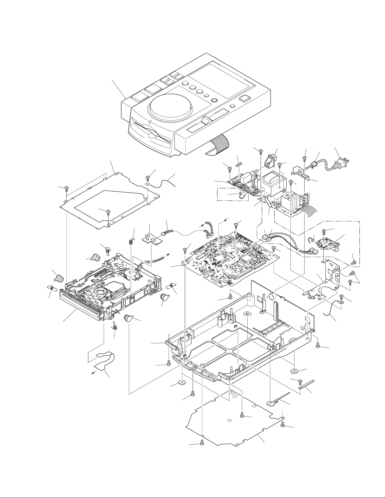
2. EXPLODED VIEWS AND PARTS LIST
NOTES : Parts marked by “ NSP ” are generally unavailable because they are not in our Master Spare Parts List.
The mark found on some component parts indicates the importance of the safety factor of the part.
Therefore, when replacing, be sure to use parts of identical designation.
Screw adjacent to mark on the product are used for disassembly.
2.1 PACKING
6
9
13 (RL type Only)
8 (KUC type Only)
1
7
2
12
11
(1) PACKING PARTS LIST
10
5
3
4
Mark No. Description Part No.
1 Pad (A) DHA1411
2 Pad (B) DHA1412
3 Pad (C) DHA1413
4 Packing Case
5 Packing Sheet Z23–026
(550 × 550 × 0.5)
6 Audio Cable (L= 1.5m) VDE1033
7 Operating Instructions
NSP 8 Limited Warranty
9 Polyethylene Bag Z21–038
(0.03 × 230 × 340)
10 Polyethylene Bag DHL1106
NSP 11 Silica Gel AEN7001
NSP 12 Caution SG DRM1199
NSP 13 Caution Card 220V
(2) CONTRAST TABLE
CDJ-100S/KUC, RL and WY are constructed the same except for the following:
No.
Symbol and Description
KUC type RL type WY type
Part No.
See Contrast table (2)
See Contrast table (2)
See Contrast table (2)
See Contrast table (2)
RemarksMark
4 Packing Case DHG1852 DHG1851 DHG1850
7 Operating Instructions (English) DRB1232 Not used Not used
7 Operating Instructions Not used DRB1229 Not used
(English/Spanish/Chinese)
7 Operating Instructions Not used Not used DRB1227
(English/French/German/Italian/
Dutch/Spanish)
NSP 8 Limited Warranty DRY1177 Not used Not used
NSP 13 Caution Card 220V Not used ARR7003 Not used
4
Page 5
KUC type Only
RL, WY types Only
30
4
31
28
28
Refer to "2.4 SLOT-IN
MECHANISM ASSY".
Refer to "2.3 EXTERIOR (2/2)".
14
28
28
19
15
28
20
9
23
22
23
22
22
22
23
28
6
28
28
24
21
3
12
28
1
27
7
8
17
31
10
32
11
28
28
25
13
28
28
2
27
5
18
28
23
28
28
26
29
16
32
28
28
6
28
A
B
B
C
C
A
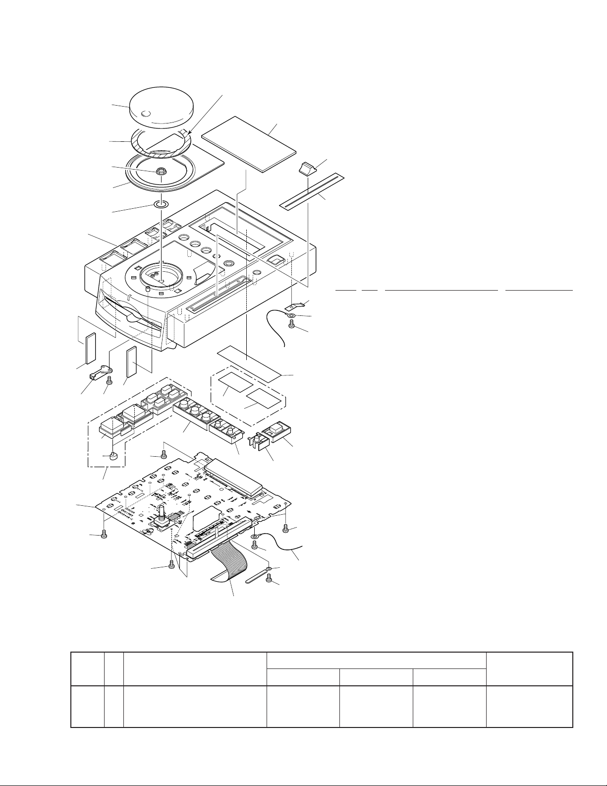
2.2 EXTERIOR (1/2)
CDJ-100S
5
Page 6
CDJ-100S
(1) EXTERIOR (1/2) PARTS LIST
Mark No. Description Part No.
1 MOTHER BOARD ASSY
2 TRANS BOARD ASSY
NSP 3 SL MECHA BOARD ASSY DWS1294
NSP 4 DIGITAL OUT BOARD ASSY
5 Strain Relief
6 Earth Lead Unit/300V DDF1010
7 Connector Assy
8 Connector Assy (2P)
9 S Flex DNP1748
10 Power Transformer
11 AC Power Cord
12 Connector Assy PF03PP–B30
13 Fuse (FU1)
NSP 14 Slot-in Mechanism Assy DXA1845
15 Insulator DEC2235
16 Insulator MO DEC2250
17 Earth Plate DNF1588
18 Cable Stay DNF1589
19 Bottom Plate
NSP 20 Chassis
21 Earth Spring DBH1398
22 Float Spring DBH1428
23 Damper DEC2236
24 Mecha Holder DNH2339
25 Power Knob DAC1895
See Contrast table (2)
See Contrast table (2)
See Contrast table (2)
See Contrast table (2)
See Contrast table (2)
See Contrast table (2)
See Contrast table (2)
See Contrast table (2)
See Contrast table (2)
See Contrast table (2)
See Contrast table (2)
Mark No. Description Part No.
26 Push Rod DEX1008
27 Screw BBZ30P080FMC
28 Screw BPZ30P080FZK
29 Screw BPZ30P140FMC
30 Nylon Rivet (3 × 4.5)
31 Binder ZCA–SKB90BK
NSP 32 Binder Z09–061
See Contrast table (2)
(2) CONTRAST TABLE
CDJ-100S/KUC, RL and WY are constructed the same except for the following:
No.
Symbol and Description
KUC type RL type WY type
1 MOTHER BOARD Assy DWM2078 DWM2079 DWM2079
2 TRANS BOARD Assy DWR1298 DWR1301 DWR1300
NSP 4 DIGITAL OUT BOARD Assy DWZ1082 Not used Not used
5 Strain Relief CM–22C CM–22B CM–22B
7 Connector Assy DKP3408 Not used Not used
8 Connector Assy (2P) DKP3409 Not used Not used
10 Power Transformer (AC120V) DTT1148 Not used Not used
10 Power Transformer Not used DTT1149 Not used
(AC110–120V/220–240V)
10 Power Transformer (AC220–240V) Not used Not used DTT1150
11 AC Power Cord PDG1063 PDG1003 PDG1003
13 Fuse (FU1) VEK1009 AEK1051 AEK1051
19 Bottom Plate DNH2341 DNH2338 DNH2338
NSP 20 Chassis DNK3562 DNK3561 DNK3553
30 Nylon Rivet (3 × 4.5) RBM–003 Not used Not used
Part No.
RemarksMark
6
Page 7
2.3 EXTERIOR (2/2)
CDJ-100S
∗1
17
5
23
12
13
15
Dyefree ME-413A: ZLX-ME413A
∗1
11
14
10
(1) EXTERIOR (2/2) PARTS LIST
Mark No. Description Part No.
25
3
22
A
4
4
22
16
19
20
18
1
22
22
6
26
27
7
21
(KUC type Only)
(WY type Only)
9
8
NSP 19 Knob A DAC1890
22
A
22
3
22
2
24
22
NSP 24 Binder Z09–061
NSP 27 Caution Label HE
1 DISPLAY BOARD ASSY DWG1503
2 36P F·F·C/60V DDD1131
3 Earth Lead Unit/300V PDF1104
4 Cushion C DEC2259
5 POM Ring DNK3556
6 Knob B DAC1891
7 Time Knob DAC1892
8 MT Knob DAC1893
9 Eject Knob DAC1894
10 Slide Sheet DAH1855
11 Display Plate DAH1886
12 Ring Plate DAH1887
13 Jog Washer DBF1001
14 Slide Knob DNK2936
15 Control Panel DNK3552
16 Disc Indicator DNK3555
17 Jog Dial DNK3625
18 Knob A Assy DXA1846
20 LED Lens PNW2019
21 65 Label
22 Screw BPZ30P080FZK
23 Nut (M9) DBN1004
25 Earth Plate VBK1070
26 Caution Label
See Contrast table (2)
See Contrast table (2)
See Contrast table (2)
(2) CONTRAST TABLE
CDJ-100S/KUC, RL and WY are constructed the same except for the following:
No.
Symbol and Description
KUC type RL type WY type
21 65 Label ORW1069 Not used Not used
26 Caution Label Not used Not used VRW1094
NSP 27 Caution Label HE Not used Not used VRW1297
Part No.
RemarksMark
7
Page 8
CDJ-100S
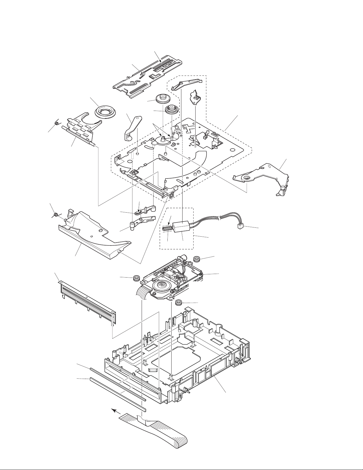
2.4 SLOT-IN MECHANISM ASSY
6
1
17
2
12
∗2
∗2
7
∗1
Dyefree ME-413A: ZLX-ME413A
∗2
Froil PN-397B: ZLB-PN397B
20
11
3
22
4
14
15
9
∗1
∗2
10
5
23
8
9
21
Refer to " 2.5 SERVO
MECHANISM ASSY SECTION".
9
16
19
18
13
To MOTHER BOARD
ASSY CN201
8
Page 9
CDJ-100S
SLOT-IN MECHANISM ASSY PARTS LIST
Mark No. Description Part No. Mark No. Description Part No.
1 Clamper Assy DXA1821
2 Clamp Spring DBH1374
3 Guide Spring DBH1375
4 Lever B DNK3558
5 Loading Motor Assy-S DEA1008
6 Main Cam DNK3407
7 Loading Gear DNK3409
NSP 8 Worm Gear DNK3410
9 Mount Bush DEB1328
10 Connector Assy PF02PY-B27
11 Clamp Arm DNK3404
12 Drive Gear DNK3565
13 Float Base Assy DXB1683
14 Disc Guide DNK3478
15 Front Sheet DED1132
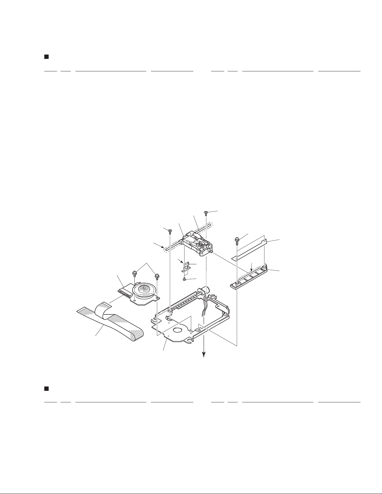
2.5 SERVO MECHANISM ASSY
6
∗2
14
1
∗3
12
16 Eject Lever DNK3548
17 Loading Lever DNK3406
18 Cushion A DEC2257
19 Cushion B DEC2258
20 Loading Base Assy-S DXX2431
21 Servo Mechanism Assy-S DXX2432
22 Lever A DNK3564
NSP 23 Loading Motor DXM1093
7
2
9
6
13
10
∗1
8
11
3
To MOTHER BOARD
SERVO MECHANISM ASSY PARTS LIST
Mark No. Description Parts No.
1 Spindle Motor DXM1084
2 Screw Guide DNK3238
3 Pulse Motor Frame DXM1085
4 …………………………
5 …………………………
6 Screw CMZ20P060FMC
7 Guide Shaft DLA1731
ASSY CN202
Mark No. Description Parts No.
NSP 12 Pickup Assy DWY1069
∗1
Dyefree ME-413A: ZLX-ME413A
∗2
Froil PN-948P: ZLB-PN948P
∗3
Froil C-1Z: ZLB-C1Z
8 Sub Guide Shaft DNK3638
9 Screw ABA7022
10 Stopper DNH2355
11 SPD Card DDX1165
13 Screw PMA20P080FMC
14 Screw PMH20P040FCC
9
Page 10
1
234
CDJ-100S
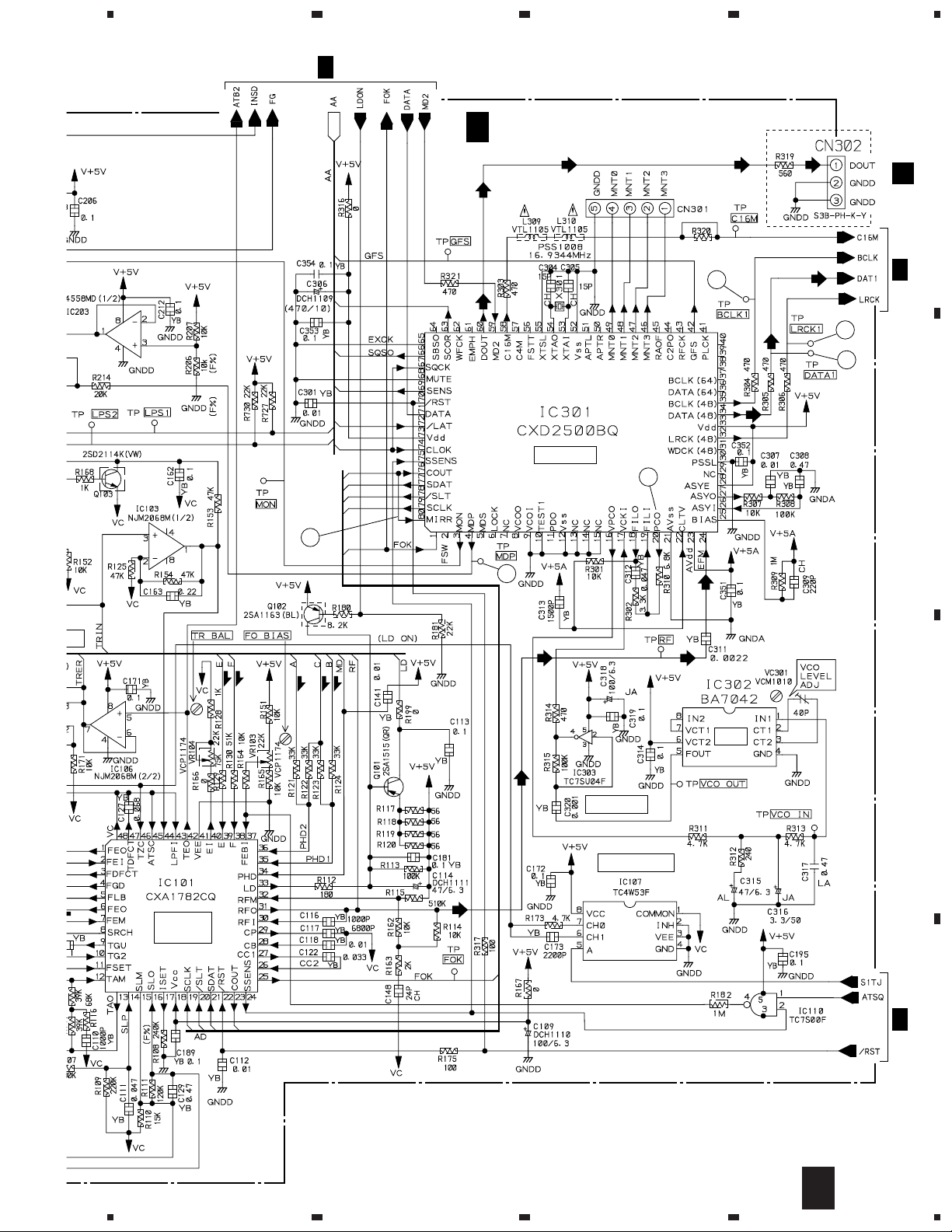
3. SCHEMATIC DIAGRAM
Note: When ordering service parts, be sure to refer to "EXPLODED VIEWS AND PARTS LIST" or "PCB PARTS LIST".
3.1 OVERALL CONNECTION DIAGRAM
A
SLOT-IN MECHANISM ASSY (DXA1845)
SERVO MECHANISM ASSY-S (DXX2432)
SPINDLE MOTOR ASSY (DXM1084)
B
PICKUP ASSY (DWY1069)
B (
MOTHER BOARD ASSY
(DWM2078: KUC type)
(DWM2079: RL and WY types)
B
1/3 to B 3/3
)
C
PULSE MOTOR
FRAME
(DXM1085)
LOADING MOTOR ASSY-S
(DEA1008)
SL MECHA BOARD ASSY
A
D
10
A
(DWS1294)
EARTH LEAD UNIT
PDF1104
1234
Page 11
5
T
B (
MOTHER BOARD ASSY
(DWM2078: KUC type)
(DWM2079: RL and WY types)
B
1/3 to B 3/3
)
67
CDJ-100S
DISPLAY BOARD ASSY
D
(DWG1503)
8
A
B
TRANS BOARD ASSY
(DWR1298: KUC type)
C
(DWR1301: RL type)
(DWR1300: WY type)
E
DIGITAL OUT
BOARD ASSY
(DWZ1082)
AC POWER CORD
PDG1015 (KUC)
PDG1003 (RL, WY)
KUC type Only
AC120V (KUC)
AC110–120V, 220–240V (RL)
AC220–240V (WY)
EARTH LEAD UNI
DDF1010
C
D
11
5
6
7
8
Page 12
1
234
CDJ-100S
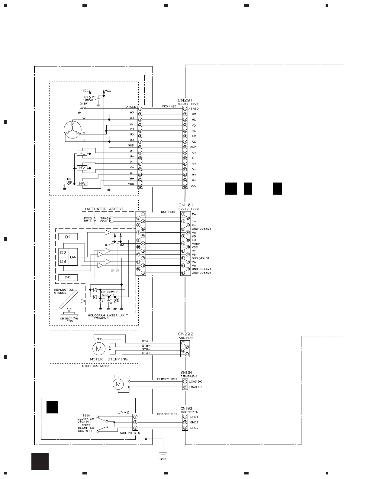
3.2 MOTHER BOARD ASSY (1/3)
A
SIGNAL ROUTE
: RF and Audio Signal Route
(F)
: Focus Servo Loop
(T)
: Tracking Servo Loop
(L)
: LOADING Drive
B
To LOADING MOTOR
ASSY
To SPINDLE MOTOR ASSY
A
CN901
(L)
(L)
7
SPINDLE DRIVE
8
6
FOCUS DC BOOST
TRACKING DC BOOST
(L)
4
(F)
(T)
(F)
C
To PICKUP ASSY
(T)
(F)
(F)
(T)
1 3
2
(L)
D
B
3/3
5
(F)
TRACKING, FOCUS
DRIVE
(T)
(T)
(T) (T)
LOADING DRIVE
(F)
(F)
(F)
(L)
(L)
(F)
(L)
(F) (F)
(L)
(T)
(L)
(T) (T)
TZC AMP
12
B 1/3
ANALOG SW
1234
Page 13
5
67
8
CDJ-100S
B
3/3
17
B
MOTHER BOARD ASSY (1/3)
(DWM2078: KUC type)
1/3
(DWM2079: RL and WY types)
DECODER
20
13
KUC ONLY
12
11
E
CN801
B
2/3
A
B
16
P
(T) (T)
(F)
SERVO
CONTROL
(F)
(F)(F)
VCO
C
INVERTER
ANALOG SW
B
3/3
D
5
6
7
8
B 1/3
13
Page 14
CDJ-100S
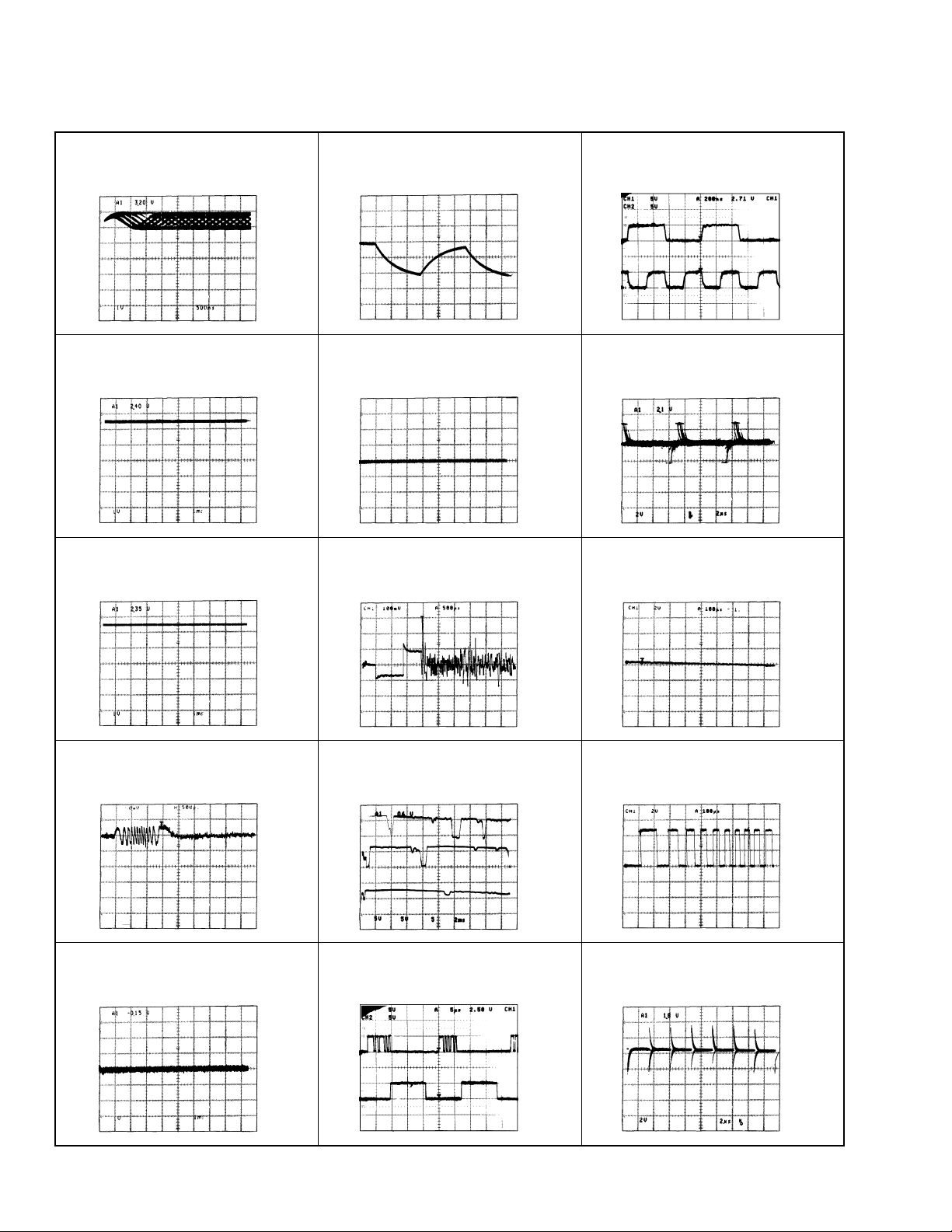
Waveforms of MOTHER BOARD ASSY (1/3)
Note : The encircled numbers denote measuring points in the schematic diagram.
1
TP1 – Pin 1 : PLAY MODE (RF)
1 V/div, 500 ns/div
1
2
TP1 – Pin 6 : PLAY MODE (FOER)
1 V/div, 1 ms/div
2
– GND
– GND
4
TP – FODR : TEST MODE
(FOCUS IN)
5 V/div, 200 ms/div
4
5
TP – TRDR : PLAY MODE
1 V/div, 1 ms/div
5
– +5V
– GND
– –5V
– GND
∗
1 14T-JUMP : After switching to the pause mode,
~
-
~
#
2 V/div, 2 µs/div
Press the manual search key.
TP – DATA1
TP – BCLK1
TP – MDP : PLAY MODE
PLAY MODE
5 V/div, 200 ns/div
– GND
– GND
#
– GND
3
TP1 – Pin 2 : PLAY MODE (TRER)
1 V/div, 1 ms/div
3
3
TP1 – Pin 2 : 14T-JUMP (∗1) MODE
(TRER)
1 V/div, 2 ms/div
3
– GND
4
TP – FODR : PLAY MODE
1 V/div, 1 ms/div
– GND
5
TP – TRDR : 14T-JUMP (∗1) MODE
1 V/div, 200 µs/div
5
6
TP – WOUT
7
TP – UOUT
8
TP – VOUT
6
7
8
-
TP – DATA1
=
TP – LRCK1
PLAY MODE
5 V/div, 2 ms/div
– GND
– GND
– GND
– GND
PLAY MODE
5 V/div, 5 µs/div
$
IC301-Pin80(MIRR) : PLAY MODE
2 V/div, 100 µs/div
$
$
IC301-Pin80(MIRR) : 14T-JUMP (∗1)
MODE
2 V/div, 100 µs/div
$
&
IC301 – Pin20 (PCO) : PLAY MODE
2 V/div, 2 µs/div
– GND
– GND
14
4
– GND
-
=
– GND
– GND
&
– GND
Page 15
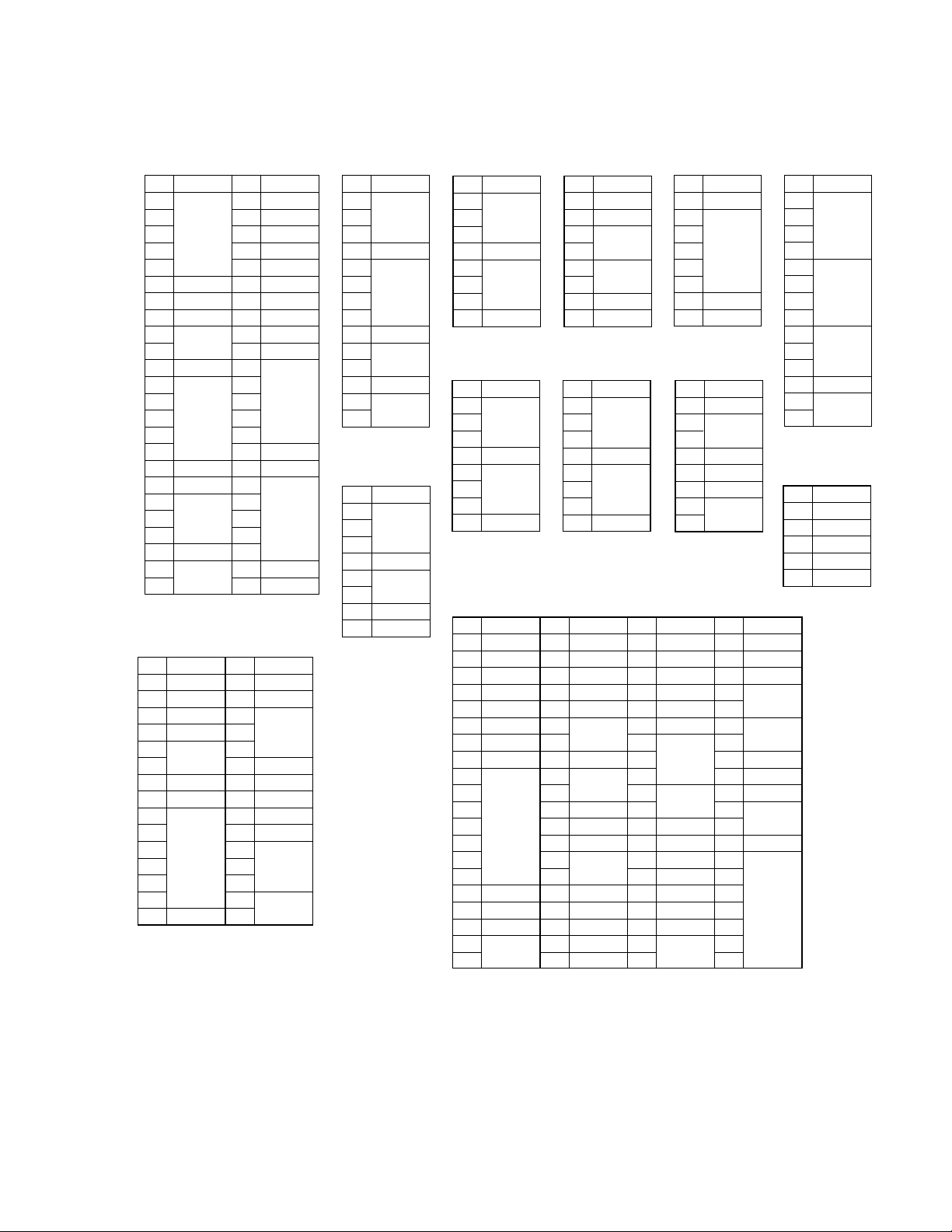
Voltages of MOTHER BOARD ASSY (1/3)
Set: DJ mode PLAY
IC101
(CXA1782CQ)
Voltage [ V ]
No.
1
2
+2.53
4
5
+2.76
+2.57
+2.78
9
+2.5
10
+0.811
12
13
+2.514
15
16
+1.217
+4.918
19
0 to +520
21
+4.922
23
0 to +5
24
IC201
(BA6849FP)
Voltage [ V ]
No.
1
0
2
+6.0
0
3
4
+6.0
5
0
6
+6.07
08
9
10
11
+2.5
12
13
14
15
+0.5
No.
25
26
27
28
29
30
31
32
33
34
35
36
37
38
39
40
41
42
43
44
45
46
47
48
No.
16
17
18
19
20
21
22
23
24
25
26
27
28
29
30
Voltage [ V ]
+4.9
+0.6
+0.7
+1.6
+2.3
+2.5
+3.5
+2.5
+3.4
0
+2.5
+2.2
0
+2.5
+2.4
+2.5
Voltage [ V ]
0
+0.5
0
+2.6
+2.5
+4.9
+2.4
+4.9
+7.5
0
IC102
(LA6520)
Voltage [ V ]
No.
1
2
0
3
–0.3
4
5
6
+1.6
7
8
9
–0.1
10
11
12
13
14
0
+8.0
–8.7
IC203
(NJM4558MD)
Voltage [ V ]
No.
1
2
+2.5
3
0
4
5
+2.6
6
7
+2.7
+4.98
IC103
(NJM2068M)
No.
IC104
(NJM2904M)
No.
IC301
(CXD2500BQ)
No.
10
11
12
13
14
15
16
19
20
Voltage [ V ]
1
2
3
4
5
7
Voltage [ V ]
1
2
3
4
5
7
Voltage [ V ]
1
2
3
4
5
6
9
+2.5
0
+2.56
+4.98
+2.5
0
+2.56
+4.98
+4.9
0
+4.9
+2.7
0
+4.9
07
+4.98
0
+2.6
+2.517
018
+2.6
IC105
(TC4W66F)
No.
1
2
3
4
5
6
7
IC106
(NJM2068M)
No.
1
2
3
4
5
7
Voltage [ V ]
No.
21
0
22
+2.5
+4.9
23
+1 to +4
24
25
+0.9
26
+2.5
27
+4.928
29
0
30
+2.531
32
0 to 5
33
+5
34
0 to 5
35
36
+2.5
+2.437
+2.538
39
0
+4.9
40
Voltage [ V ]
+2.6
+2.5
0
+2.5
0
+4.98
Voltage [ V ]
+2.5
0
+2.56
+4.98
No.
41
42
43
44
45
46
47
49
50
51
52
53
54
55
56
59
60
IC107
(TC4W53F)
Voltage [ V ]
No.
1
2
3
4
5
6
7
IC302
(BA7042)
Voltage [ V ]
No.
1
2
3
4
5
6
7
8
Voltage [ V ]
+2.3
+4.9
+2.5
0
+4.9
+4.4
048
+1.2
0
+2.6
+2.7
0
+2.8
+1.457
+2.158
0
+2.5
0
+2.5
+4.98
+2.4
+2.1
0
+3.5
+4.9
+2.4
No.
61
62
63
64
65
66
67
69
70
71
72
73
74
75
76
77
78
79
80
CDJ-100S
IC108
(LA6520)
No.
1
2
3
4
5
6
7
8
9
10
11
12
13
14
IC303
(TC7SU04F)
No.
1
2
3
4
5
Voltage [ V ]
0
+2.5
0 to +5
0
0 to +5
068
0 to +5
+4.9
0 to +5
+4.9
0 to +5
Voltage [ V ]
0
+2.5
0
+8.0
–8.7
Voltage [ V ]
0
+2.5
0
+2.6
+4.9
15
Page 16

1
234
CDJ-100S
3.3 MOTHER BOARD ASSY (2/3)
MOTHER BOARD ASSY (2/3)
A
B 2/3
B 1/3
B
(DWM2078: KUC type)
(DWM2079: RL and WY types)
IC402 (MB814800–70PJ)
Pin No.
Voltage [ V ]
Pin No.
Voltage [ V ]
DRAM (512k × 8 bit)
SIGNAL ROUTE
: RF and Audio Signal Route
1
2 3 4 5 6 7 8 9 10 11 12 13 14
+4.9 +4.90 to +5
15 16 17 18 19 20 21 22 23 24 25 26 27 28
00 0
0 to +5 0 to +5
Set: DJ MODE PLAY
0 to +50
! IC401 Pin 24 (SDA)
@ IC401 Pin 25 (SCL)
PLAY MODE 5 V/div, 20 µs/div
!
@
– GND
– GND
14 15
DSP
C
D
16
B 2/3
1234
Page 17

5
67
8
CDJ-100S
B 3/3
IC401 (MN19413A–P)
Pin No.
1
2
4
6
7
8
9
10
12
13
14
16
17
18
19
20
21
22
23
24
Voltage [ V ]
+1.5
+4.93
0 to +55
0
+2.4
011
0 to +515
+4.9
0
0 to +5
025
Pin No.
28
29
30
32
33
34
35
36
38
39
41
42
43
44
46
47
48
49
Voltage [ V ]
0 to +537
0 to +545
026
+4.927
031
040
050
MUTE
Pin No.
51
52
53
54
55
56
57
58
59
60
71
72
Voltage [ V ]
0 to +5
Set: DJ MODE PLAY
+4.9
061
+2.562
+2.663
+4.964
+2.465
+2.566
067
+4.968
069
+4.970
0
+1.473
+4.974
075
Pin No.
76
77
78
79
80
81
82
83
84
90
92
93
96
99
100
Voltage [ V ]
+4.9
+4.9
+1.085
+2.486
+1.088
+2.589
+4.991
+2.394
+1.5
+4.998
+1.5
0
0
0
087
0
0
095
097
B
C
J11
A
LPF
C
+7.5
0
0
+1.2
0
+1.2
5
6
7
8
B 2/3
17
D
Page 18

1
234
CDJ-100S
3.4 MOTHER BOARD ASSY (3/3)
Waveforms
9
A
TP – STA +
0
TP – STA –
9
0
%
TP – RST : POWER ON
2 V/div, 5 ms/div
%
B
%
TP – RST : POWER OFF
2 V/div, 10 ms/div
PLAY MODE
5 V/div, 5 µs/div
– GND
– GND
– GND
B
3/3
10 9
To Pulse Motor Frame
AUTO TRACKING BALANCE
MOTHER BOARD ASSY (3/3)
(DWM2078: KUC type)
(DWM2079: RL and WY types)
STEPPING DRIVE
%
– GND
^
TP – RST3 : POWER ON
2 V/div, 1 µs/div
C
^
^
TP – RST3 : POWER OFF
2 V/div, 200 ms/div
– GND
IC901
(NJM2904M)
Pin No.
1
2
3
4
6
7
8
Voltage [ V ]
+2.5
0
+2.45
+2.5
+2.2
+4.9
IC902
(NJM2904M)
Voltage [ V ]
Pin No.
+2.2
1
2
+2.5
3
0
4
5
+2.5
6
+2.6
7
+7.4
8
Set: DJ MODE PLAY
18
^
– GND
D712, D713,
D
B
18
B 3/3
1234
2/3
D729, D730: 1SS355
Page 19

5
IC206
(MPC17A85ZVM)
1
Pin No.
Voltage [ V ]
Pin No.
Voltage [ V ]
Pin No.
Voltage [ V ]
Pin No.
Voltage [ V ]
2345678
0 +4.6 +4.9 0 +1.5 +0.2 +0.4 +0.5
9 10111213141516
+0.4 +4.9 +1.50 +0.1 +0.5 0+4.8
17
18 19 20 21 22 23 24
+0.2+3.2 +0.5
25 26 27 28 29 30
+2.5 +4.9 +4.9
Set: DJ MODE PLAY
+19.3
+4.8
0 to +5
+11.9
+7.2+1.4
67
8
CDJ-100S
IC701 (PD4977B)
Voltage [ V ]
Voltage [ V ]
Voltage [ V ]
Voltage [ V ]
1
Pin No.
Pin No.
Pin No.
Pin No.
2 3 4 5 6 7 8 9 10 11 12 13 14
21 22 23 24 25 26 27 28 29 30 31 32 33 34
+4.9 +4.9 +2.4 +2.5 +2.5+2.2+2.3 +2.6 +2.50000
0 to +5
41
42 43 44 45 46 47 48 49 50 51 52 53 54
+4.9 +3.0 +4.9
0
61 62 63 64 65 66 67 68 69 70 71 72 73 74
0
+4.9
–30.5 to +5 –30.5 to +5 –30.5 to +5
+4.900 0 0
00+4.9 +4.8
0 to +5
–30.5 –30.5
SIGNAL ROUTE
(L)
Set: DJ MODE PLAY
15 16 17 18 19 20
0 to +5 0 to +5–30.5 to +5
+4.9
35 36 37 38 39 40
55 56 57 58 59 60
+4.9
75 76 77 78 79 80
: LOADING DRIVE
+4.9
(L)(L)
(L)(L)
A
B
19
IC701
PD4977B
SYSTEM CONTROL
EXCEPT KUC
KUC ONLY
B
1/3
E
CN802
C
D
CN601
D
5
6
7
FFC DDD1131
B 3/3
8
19
Page 20

1
CDJ-100S
3.5 TRANS BOARD ASSY
234
A
B
CN705
B
2/3
+5V REGULATOR
HEAT SINK
CAUTION: FOR CONTINUED PROTECTION AGAINST RISK OF FIRE.
REPLACE ONLY WITH SAME TIME NO. ICP-N25, MFD BY
ROHM CO., LTD. FOR IC91.
CAUTION: FOR CONTINUED PROTECTION AGAINST RISK OF
C
TRANS BOARD ASSY
(DWR1298: KUC type)
C
(DWR1301: RL type)
(DWR1300: WY type)
D
FIRE. REPLACE ONLY WITH SAME TIME NO. ICPN10, MFD BY ROHM CO., LTD. FOR IC92.
SIGNAL ROUTE
: RF and Audio Signal Route
20
C
1234
Page 21

5
67
8
CDJ-100S
POWER TRANSFORMER
DTT1148
POWER TRANSFORMER
DTT1149
NOTE FOR FUSE REPLACEMENT
CAUTION: FOR CONTINUED PROTECTION
AGAINST RISK OF FIRE.
REPLACE ONLY WITH SAME
TIME AND RATINGS ONLY.
NOTE FOR FUSE REPLACEMENT
CAUTION: FOR CONTINUED PROTECTION
AGAINST RISK OF FIRE.
REPLACE ONLY WITH SAME
TIME AND RATINGS ONLY.
A
AC POWER CORD
PDG1015
AC120V
60 Hz
B
RL type
POWER TRANSFORMER
DTT1150
NOTE FOR FUSE REPLACEMENT
CAUTION: FOR CONTINUED PROTECTION
AGAINST RISK OF FIRE.
REPLACE ONLY WITH SAME
TIME AND RATINGS ONLY.
AC POWER CORD
PDG1003
AC110–120V/
220–240V
50/60 Hz
C
WY type
AC POWER CORD
PDG1003
AC220–240V
50/60 Hz
D
C
5
6
7
8
21
Page 22

1
234
CDJ-100S
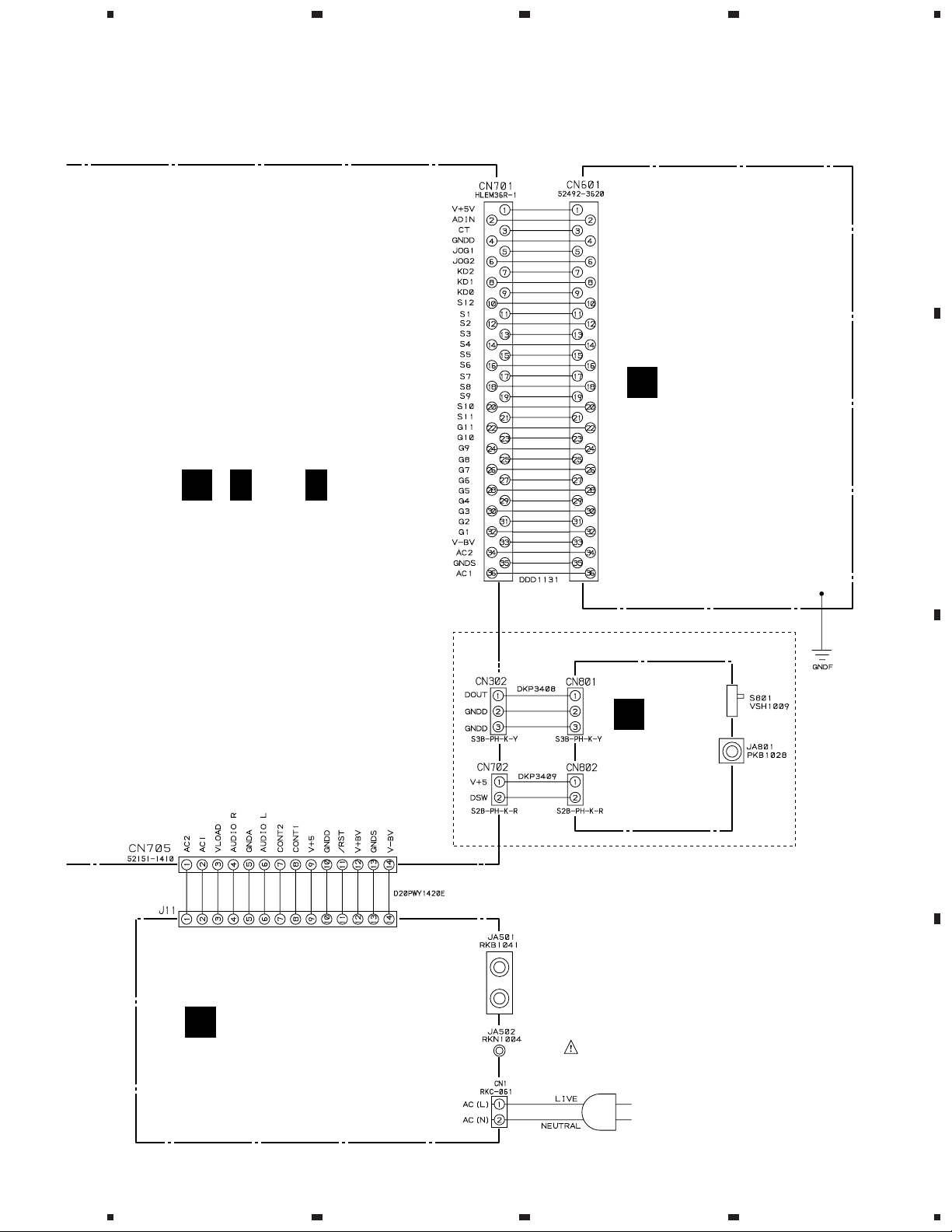
3.6 DISPLAY BOARD and DIGITAL OUT BOARD ASSEMBLIES
A
D FLIP–FLOP
B
FL HOLDER
DEB1396 × 2
C
D
B
3/3
CN701
DISPLAY BOARD ASSY
D
(DWG1503)
LED ON/OFF
Short: TEST MODE
Short: AGING MODE
ENCODER
22
D
1234
Page 23

5
67
8
CDJ-100S
(GRN)
(YEL)
SWITCHES:
S601: TRACK SEARCH (4)
S602: SEARCH (1)
S603: PLAY/PAUSE (6)
S604: TRACK SEARCH (¢)
S605: SEARCH (¡)
S606: CUE
S607: DIGITAL JOG BREAK (JET)
S608: MASTER TEMPO
S609: DIGITAL JOG BREAK (ZIP)
S610: DIGITAL JOG BREAK (WAH)
S611: EJECT (0)
S613: TIME MODE/AUTO CUE
S615: DIGITAL JOG BREAK (HPLD)
(GRN)
LED HOLDER
(GRN)
S601, S602, S604, S605,
S607–S611, S613, S615: VSG1008
S603, S606: DSG1063
SLIDER VR
A
B
KUC type Only
B
1/3
CN302
B
3/3
CN702
5
DIGITAL OUT BOARD ASSY
E
(DWZ1082)
C
SIGNAL ROUTE
: RF and Audio Signal Route
EARTH
PLATE
ANK1074
D
6
7
EARTH LEAD UNIT
E
8
D
23
Page 24

1
234
CDJ-100S
4. PCB CONNECTION DIAGRAM
4.1 SL MECHA BOARD, MOTHER BOARD, TRANS BOARD and
DIGITAL OUT BOARD ASSEMBLIES
A
SIDE A
MOTHER BOARD ASSY
B
SLOT-IN MECHANISM
ASSY
Stepping Motor
B
Loading Motor Assy
A
SL MECHA BOARD
ASSY
C
Spindle Motor Assy
Pickup Assy
(DNP1873–C)
D
VR101–VR104 VC301
24
IC206
IC103 IC104 IC105
A
B
1234
IC303 IC302 IC405 IC109 Q403
IC106Q103
IC107 IC402
IC201 IC110 IC902 IC901 IC108
IC101 Q101 Q102 IC701
IC401IC301IC203
Q404 Q401 Q402
Page 25

5
67
8
CDJ-100S
SIDE A
(DNP1872–C)
C
TRANS BOARD ASSY
AC POWER CORD
DIGITAL OUT
E
BOARD ASSY
(DNP1873–C)
KUC type Only
NOTE FOR PCB DIAGRAMS:
1. Part numbers in PCB diagrams match those in the schematic
diagrams.
2. A comparison between the main parts of PCB and schematic
diagrams is shown below.
Symbol in PCB
Diagrams
BCE
BCE
Symbol in Schematic
Diagrams
BCE
BCE
BCEBCE
Part Name
Transistor
Transistor
with resistor
A
B
Q401 Q402 Q406
D
CN601
IC95
IC94
IC93
Q1
IC91
IC23
IC92
(DNP1873–C)
DGSDGS
DGS
3. The parts mounted on this PCB include all necessary parts
for several destination.
For further information for respective destinations, be sure
to check with the schematic diagram.
4. Viewpoint of PCB diagrams
P. C. Board Chip Part
CapacitorConnector
Field effect
transistor
Resistor array
3-terminal
regulator
SIDE A
SIDE B
C
D
B
5
6
7
C E
8
25
Page 26

1
CDJ-100S
234
DIGITAL OUT
SIDE B
E
BOARD ASSY
A
C
TRANS BOARD ASSY
(DNP1873–C)
B
C
D
(DNP1873–C)
26
C E
1234
Page 27

5
67
8
CDJ-100S
MOTHER BOARD ASSY
B
SIDE B
A
(DNP1872–C)
B
C
D
B
5
6
7
8
27
Page 28
1
234
CDJ-100S
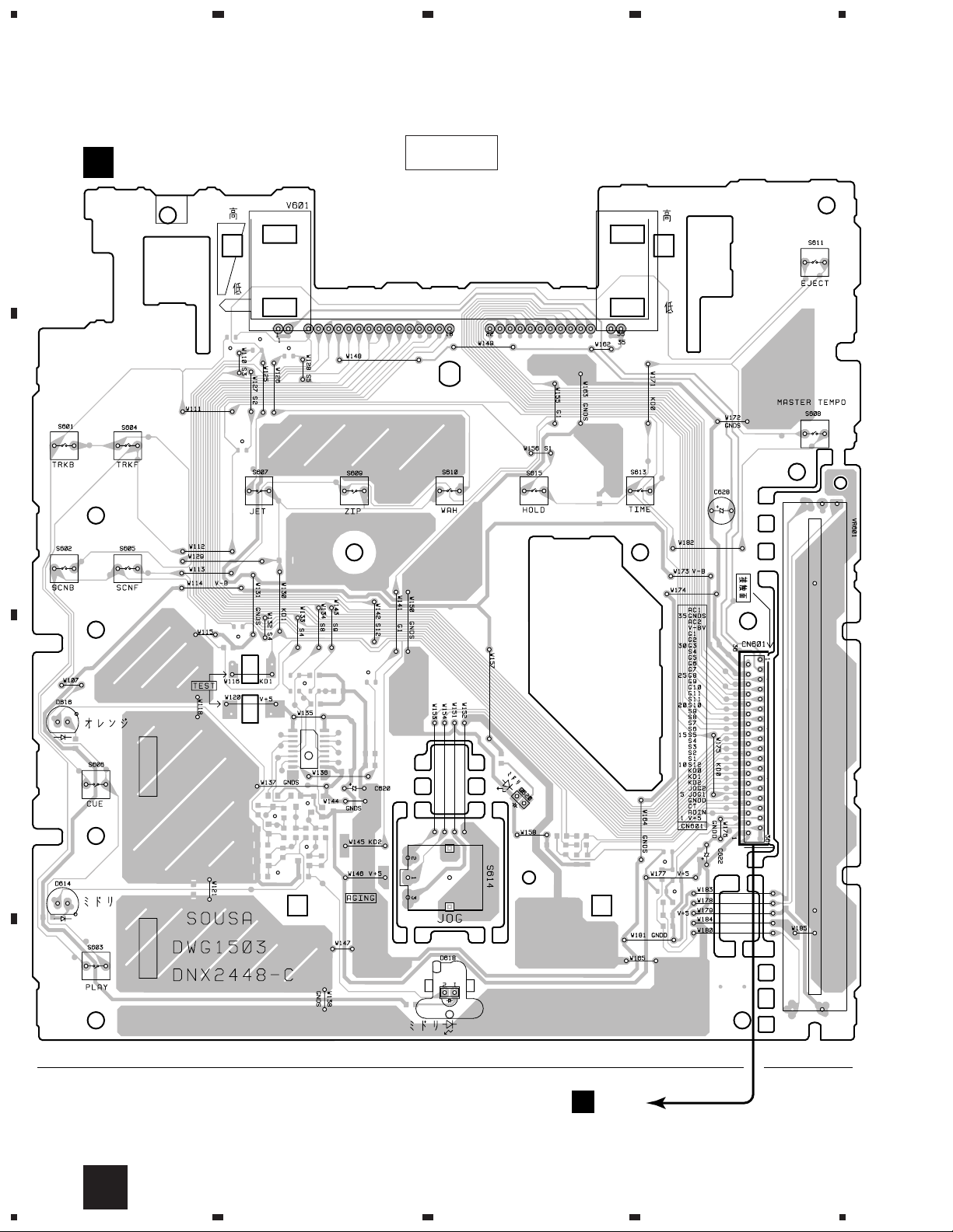
4.2 DISPLAY BOARD ASSEMBLY
A
B
DISPLAY BOARD ASSY
D
SIDE A
C
D
(DNP1873–C)
28
VR601
CN701
B
D
1234
Page 29

1
23
4
CDJ-100S
DISPLAY BOARD ASSY
D
SIDE B
A
B
(DNP1873–C)
C
IC602
Q608 Q609
Q610 Q602
Q603 Q601
D
1
2
3
4
29
D
Page 30

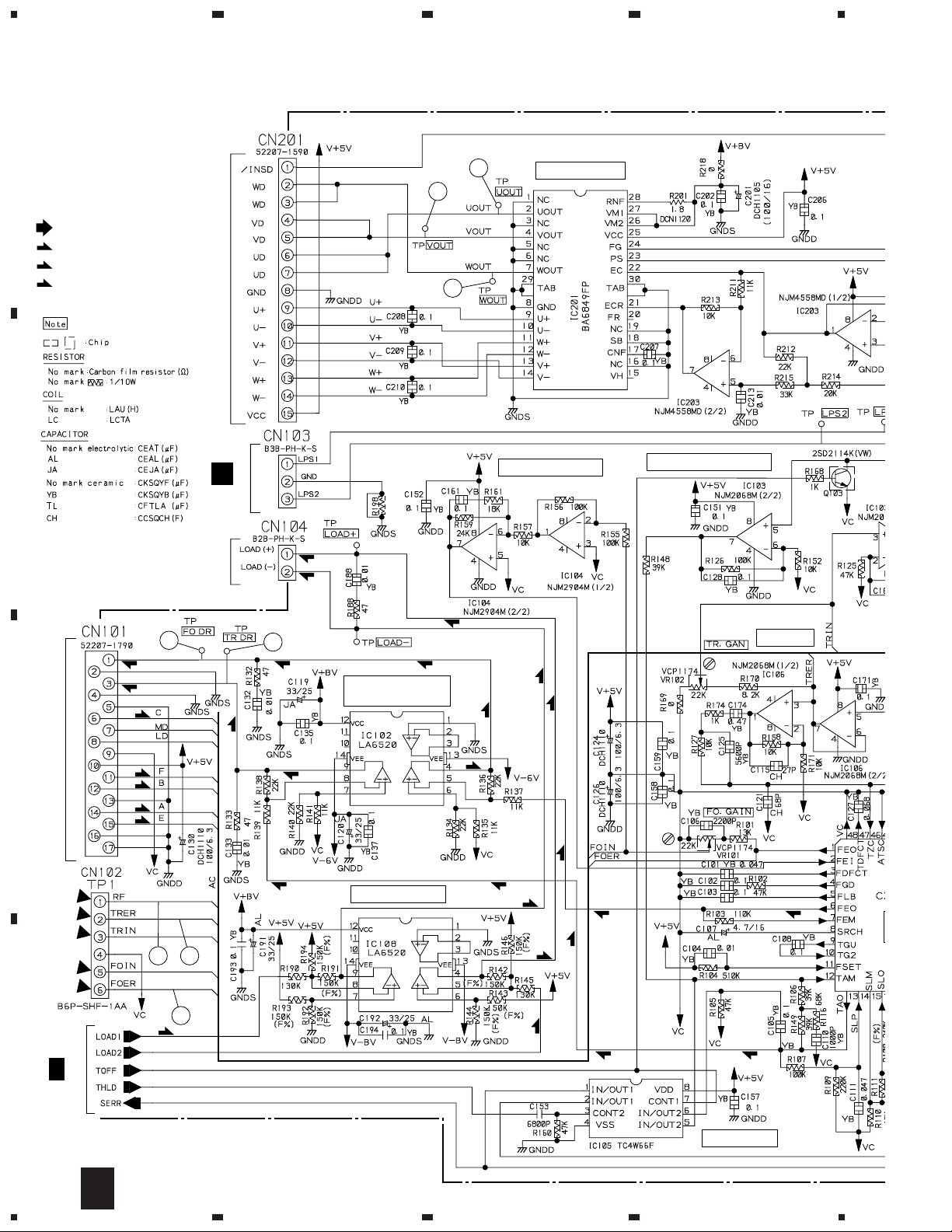
CDJ-100S
5. PCB PARTS LIST
NOTES : ÷ Parts marked by “ NSP ” are generally unavailable because they are not in our Master Spare Parts List.
÷ The
÷ When ordering resistors, first convert resistance values into code form as shown in the following examples.
LIST OF WHOLE PCB ASSEMBLIES
mark found on some component parts indicates the importance of the safety factor of the part.
Therefore, when replacing, be sure to use parts of identical designation.
Ex. 1 When there are 2 effective digits (any digit apart from 0), such as 560 ohm and 47k ohm (tolerance is shown by
J = 5%, and K = 10%).
560 Ω = 56 × 10
47k Ω = 47 × 10
0.5 Ω = R50 ...................................................................... RN2H Â 5 0 K
1 Ω = 1R0 ......................................................................... RS1P 1 Â 0 K
Ex. 2 When there are 3 effective digits (such as in high precision metal film resistors).
5.62k Ω = 562 × 10 1 = 5621 ........................................... RN1/4PC 5 6 2 1 F
1
= 561................................................... RD1/4PU 5 6 1 J
3
= 473 .................................................. RD1/4PU 4 7 3 J
Mark
NSP SUB BOARD ASSY DWX1892 DWX1891 DWX1898
NSP SL MECHA BOARD ASSY DWS1294 DWS1294 DWS1294
NSP DIGITAL OUT BOARD ASSY DWZ1082 Not used Not used
Symbol and Description
KUC type RL type WY type
MOTHER BOARD ASSY DWM2078 DWM2079 DWM2079
DISPLAY BOARD ASSY DWG1503 DWG1503 DWG1503
TRANS BOARD ASSY DWR1298 DWR1301 DWR1300
Part No.
CONTRAST OF PCB ASSEMBLIES
MOTHER BOARD ASSY
B
DWM2078 and DWM2079 are constructed the same except for the following:
Mark
Symbol and Description
DWM2078 DWM2079
C709 CKSQYB103K50 Not used
C719, C720 CKSQYB104K25 Not used
R319 RS1/10S561J Not used
R708 Not used RS1/10S223J
R738 RS1/10S102J Not used
Part No.
Remarks
Remarks
CN302 S3B-PH-K-Y Not used
CN702 S2B-PH-K-Y Not used
TRANS BOARD ASSY
C
DWR1298, DWR1301 and DWR1300 are constructed the same except for the following:
Mark Symbol and Description
DWR1298 DWR1301 DWR1300
S2 Voltage Selector Not used DSA1026 Not used
30
Part No.
Remarks
Page 31

PARTS LIST FOR CDJ-100S/KUC
CDJ-100S
Mark No. Description Part No.
B
MOTHER BOARD ASSY
SEMICONDUCTORS
IC201 BA6849FP
IC302 BA7042
IC101 CXA1782CQ
IC301 CXD2500BQ
IC102, IC108 LA6520
IC402 MB814800-70PJ
IC401 MN19413A-P
IC206 MPC17A85ZVM
IC103, IC106 NJM2068M
IC104, IC901, IC902 NJM2904M
IC203, IC405 NJM4558MD
IC701 PD4977B
IC107 TC4W53F
IC105 TC4W66F
IC110 TC7S00F
IC303 TC7SU04F
Q102 2SA1163
Q101 2SA1515
Q103, Q401, Q402, Q405, Q406 2SD2114K
Q403 DTC124EK
D712, D713, D729, D730 1SS355
D735–D738, D901–D904 1SS355
COILS AND FILTERS
L201 (39 µH) DTL1070
L401 LFA220J
L309, L310 VTL1105
CAPACITORS
C304, C305, C445, C446 CCSQCH150J50
C309 CCSQCH221J50
C148 CCSQCH240J50
C115 CCSQCH270J50
C453–C456 CCSQCH390J50
C451, C452 CCSQCH471J50
C121 CCSQCH680J50
C705, C714 CEAL101M6R3
C191, C192 CEAL330M25
C315, C415 CEAL470M6R3
C107 CEAL4R7M16
C91, C92 CEJA101M16
C219, C318, C401 CEJA101M6R3
C404 CEJA1R0M50
C405, C407, C463, C464 CEJA220M25
C119, C120 CEJA330M25
C316 CEJA3R3M50
C317 CFTLA474J50
C110, C116, C320 CKSQYB102K50
C104, C112, C118, C132, C133 CKSQYB103K50
C141, C188, C213, C220–C224 CKSQYB103K50
C231, C301, C307, C403, C421 CKSQYB103K50
C702, C709, C905 CKSQYB103K50
C102, C103, C105, C108, C113 CKSQYB104K25
C128, C135, C137, C151, C152 CKSQYB104K25
Mark No. Description Part No.
C157–C159, C161, C162 CKSQYB104K25
C171, C172, C181, C189 CKSQYB104K25
C193–C195, C202, C206–C210 CKSQYB104K25
C212, C218, C314, C319 CKSQYB104K25
C351–C354, C402, C406 CKSQYB104K25
C408–C412, C416, C433, C434 CKSQYB104K25
C481, C482, C701, C704, C706 CKSQYB104K25
C713, C717, C719, C720 CKSQYB104K25
C901, C902, C94 CKSQYB104K25
C907 CKSQYB105K10
C711, C712 CKSQYB122K50
C313 CKSQYB152K50
C106, C173, C311 CKSQYB222K50
C163, C903, C904 CKSQYB224K16
C225 CKSQYB332K50
C122 CKSQYB333K50
C111 CKSQYB473K25
C101, C312, C703 CKSQYB473K50
C129, C174, C308 CKSQYB474K16
C125 CKSQYB562K50
C117, C153 CKSQYB682K50
C127 CKSQYB683K25
C201 (100 µF/16V) DCH1105
C93 (330 µF/ 16V) DCH1108
C306 (470 µF/ 10V) DCH1109
C109, C124, C126, C130 DCH1110
(100 µF/6.3V)
C114 (47 µF/6.3V) DCH1111
VC301 (40 pF) VCM1010
RESISTORS
R403, R404 (82 Ω) ACN7049
R223, R224 (1.6 Ω, 1/4W) DCN1109
R201 (1.8 Ω, 1/4W) DCN1120
R461, R462 RN1/10SE2202D
R206, R207 RS1/10S1002F
R142–R144, R146, R191–R194 RS1/10S1503F
R108 RS1/10S2403F
VR101–VR104 (22 kΩ) VCP1174
Other Resistors RS1/10S J
OTHERS
CN201 CONNECTOR (15P) 52207-1590
CN101 CONNECTOR (17P) 52207-1790
CN104 CONNECTOR POST (2P) B2B-PH-K-S
CN103 CONNECTOR POST (3P) B3B-PH-K-S
CN102 TOP POST (6P) B6P-SHF-1AA
P.C. BOARD DNP1872
X401 (20 MHz) DSS1104
X701 (4.19 MHz) DSS1105
CN701 FFC CONNECTOR 36P HLEM36R-1
X301 (16.9344 MHz) PSS1008
CN202 FFC CONNECTOR 4P VKN1235
31
Page 32

CDJ-100S
Mark No. Description Part No.
D
DISPLAY BOARD ASSY
SEMICONDUCTORS
IC602 HD74HC175FP
Q601–Q603 2SC2412K
Q608–Q610 PDTA124EK
D601, D602, D604–D608 1SS355
D610–D613, D625, D691 1SS355
D620 GL3EG43
D618 MPG4361F
D614 SLP3118C51H
D616 SLP4118C51H
SWITCHES AND RELAYS
S603, S606 DSG1063
S614 DSX1051
S601, S602, S604, S605 VSG1008
S607–S611, S613, S615 VSG1008
CAPACITORS
C628 CEJA220M50
C602–C604, C609, C614, C615 CKSQYB103K50
C608, C610, C613, C616, C618 CKSQYB104K25
RESISTORS
VR601 (10 kΩ–B) DCV1009
Other Resistors RS1/10S J
OTHERS
CN601 FFC CONNECTOR 36P 52492-3620
V601 FL INDICATOR TUBE DEL1031
C
TRANS BOARD ASSY
FL HOLDER DEB1396
SEMICONDUCTORS
IC92 ICP-N10
IC91 ICP-N25
IC23 PQ05RR12
Q1 2SB1566
D11–D14, D52 11E2 (TB2)
D502 1SS355
D54 MTZJ27A
D55 MTZJ33B
COILS AND FILTERS
L1 VTL-004
L501, L502 VTL1105
Mark No. Description Part No.
C32 CEAT471M6R3
C12, C23, C24, C591, C83 CKSQYB104K25
C505 CKSQYF103Z50
C11, C13–C17, C56 CKSQYF104Z50
C501, C502 CQMA152J50
RESISTORS
R60 RD1/4VM222J
R551 RD1/4VM271J
Other Resistors RS1/10S J
OTHERS
J11 14P PARALLEL WIRE D20PWY1420E
JA501 PIN JACK 2P RKB1041
JA502 JACK (REMOTE) RKN1004
H1, H2 FUSE HOLDER RKR1003
A
SL MECHA BOARD ASSY
HEAT SINK DNG1077
TERMINAL 2P RKC-061
PCB BINDER VEF1040
SWITCHES AND RELAYS
S901, S902 DSG1017
OTHERS
CN901 KR CONNECTOR 3P S3B-PH-K-S
DIGITAL OUT BOARD ASSY
E
SEMICONDUCTORS
IC801 TC74HCU04AF
COILS AND FILTERS
L801 PTL1003
SWITCHES AND RELAYS
S801 VSH1009
CAPACITORS
C806 CEJA101M6R3
C805 CEJA470M35
C804, C807 CKSQYB103K50
C801, C808, C809 CKSQYB104K25
RESISTORS
All Resistors RS1/10S J
SWITCHES AND RELAYS
S1 RSA1001
CAPACITORS
C1–C3 (10000 pF/AC250V) ACG7020
C25 CEAT102M16
C21 CEAT103M16
C55 CEAT220M50
C52, C54 CEAT221M50
32
OTHERS
JA801 PIN JACK 1P PKB1028
Page 33

6. ADJUSTMENT
Adjustment points
1.2.3.4.5.6.
CD TEST DISC
8-cm DISC
(With at least about
20 minutes recording)
screwdriver
(small)
Precise
screwdriver
screwdriver
(medium)
screwdriver
(large)
39 kΩ
0.001 µF
Low-frequency
oscillator
Dual-trace
oscilloscope
(10 : 1 probe)
Low pass filter 1
(39 kΩ + 0.001 µF)
39 kΩ
0.0018 µF
100 kΩ
Low pass filter 2
(39 kΩ + 0.0018 µF)
Resistor
(100 kΩ)
= Page 36~38
2.3.4.5.6. = Page 36~38
Exchange
MOTHER BOARD ASSY
Exchange
SERVO MECHANISM ASSY
When
6.1 PREPARATIONS
6.1.1 Jigs and Measuring Instruments
6.1.2 Necessary Adjustment Points
CDJ-100S
33
Page 34

CDJ-100S
6.2 ADJUSTMENT
6.2.1 How to Start/Cancel Test Mode
[ Precautions for Test Mode ]
(1) If a soiled or damaged disc is played back and a GFS error is generated, the system may not perform a STOP operation and may run out of
control, although muting ON/OFF will be performed. If the system does run out of control, press the CUE key to switch the power OFF.
(2) Do NOT press any key while an OPEN/CLAMP, SPINDLE KICK, or FOCUS SEARCH operation is in progress. Be sure to wait until the
operation is completed before calling the next operation.
TEST MODE : ON
SIDE B
DISPLAY BOARD ASSY
TEST MODE : PLAY
TEST DISC : YEDS-7
inwards outwards
Pickup Move
TEST MODE : DISPLAY
Switch Status Display
(W116)
(W120)
Short Point
V+5
KD1
Focus servo : ON
Spindle motor : START
Spindle servo : CLOSE
OFF
ON
KD1
(W116)
V+5
(W120)
Short Point
SIDE B
DISPLAY BOARD ASSY
CLOSE OPEN
Tracking servo :
SLOT-IN MECHANISM Operation Status
EJECT:
LOAD:
TEST MODE : STOP = CANCEL
STOP all operations.
34
INSIDE SW
S901 SW
S902 SW
Page 35

6.2.2 Test Mode Key Locations
RF Adjustment Mode (Outer circumference feed)
Tracking Balance Adjustment Mode (Center circumference feed)
Note: The tracking servo is OFF.
Fine movement in direction towards the
outer circumference of the carriage
Fine movement in direction towards the
inner circumference of the carriage
Focus ON
Carriage towards the outer circumference
Carriage towards the inner circumference
STOP All Operation
CDJ-100S
LD ON
Tracking, Spindle Servo ON
6.2.3 Adjustment Location
MOTHER BOARD ASSY
VR101 : FO GAIN
VR102 : TR GAIN
VR103 : FO BIAS
VR104 : TR BAL
VC301 : VCO LEVEL
TP1
1 RF
2 TRER
3 TRIN
4 VC
5 FOIN
6 FOER
CN102
1
2
3
4
5
6
VR103
VR104
VR102
VR101
1
CN102
6
IC302
45
8
1 (TP VCO IN)
IC301
IC201
REAR
SIDE A
VC301
IC401
IC402
IC701
DISPLAY BOARD ASSY
SIDE B
TEST
FRONT
35
Page 36

CDJ-100S
6.2.4 Check and Adjustment
1. VCO Adjustment
Test mode
None disc
START
IC302 Pin 1
TP (VCO IN)
GND
MOTHER BOARD ASSY
1
MOTHER BOARD ASSY
Player
VC301
Probe (10:1)
GND
Note: Adjustment of VC301 may not be made if the
SLOT-IN MECHANISM ASSY is installed.
Before adjustment, remove the SLOT-IN
MECHANISM ASSY.
DC voltage
2.5±0.2V
Oscilloscope
DC Mode
V: 50mV/div
H: 10mSec/div
2. Focus BIAS Adjustment
Test mode
None disc
START
TP1
(CN102)
FOER
MOTHER BOARD ASSY
VC
6
4
Player
VR103
MOTHER BOARD ASSY
Probe (10:1)
GND
DC voltage
0±50mV
Oscilloscope
DC Mode
V: 5mV/div
H: 10mSec/div
36
Page 37

4. RF Level Adjustment
1
2
3. Tracking Error Barance Adjustment
Probe (10:1)
VR104
A=B
Oscilloscope
DC Mode
V: 10mV/div
H: 5mSec/div
START
TP1
(CN102)
Player
TRER
VC
39kΩ
0.001µF
Low pass filter 1
Test mode
FOCUS servo
SPDL servo
TRKG servo
=
=
=
CLOSE
CLOSE
OPEN
TEST DISC
PLAY
R=35
VC
A
B
GND
GND
Player
TP1
(CN102)
RF
VC
START
Probe (10:1)
Oscilloscope
AC Mode
V: 50mV/div
H: 10mSec/div
MOTHER BOARD ASSY
MOTHER BOARD ASSY
MOTHER BOARD ASSY
4
VR
1.1VP-P
±0.2V
Test mode
FOCUS servo
SPDL servo
TRKG servo
=
=
=
CLOSE
CLOSE
CLOSE
TEST DISC
PLAY
PICKUP ASSY
LD POWER
TIME Key - ON
Disc: Outer circumference
4
6.2.4 Check and Adjustment
CDJ-100S
37
Page 38

CDJ-100S
5. Focus Servo Loop Gain Adjustment
6.2.4 Check and Adjustment
Test mode
FOCUS servo
SPDL servo
TRKG servo
TEST DISC
Disc: Center circumference
=
=
=
WAH Key - ON
PLAY
START
TP1
(CN201)
FOER
MOTHER BOARD ASSY
FOIN
VC
6
5
4
CLOSE
CLOSE
CLOSE
MOTHER BOARD ASSY
Player
100kΩ
0.0018µF
Low pass filter 2
VR101
39kΩ
UNDER
Probe (10:1)
Probe (10:1)
GND
GND
JUST
Lissajous Waveform
Oscilloscope
X-Y Mode
X: 20mV/div
Y: 5mV/div
Low-frequency
oscillator
1.2kHz
1Vp-p
GND
UPPER
6. Tracking Servo Loop Gain Adjustment
Test mode
FOCUS servo
SPDL servo
TRKG servo
TEST DISC
Disc: Center circumference
START
TRER
TRIN
MOTHER BOARD ASSY
WAH Key - ON
PLAY
TP1
(CN201)
2
3
VC
4
=
=
=
CLOSE
CLOSE
CLOSE
VR102
MOTHER BOARD ASSY
Player
39kΩ
100kΩ
0.001µF
Low pass filter 1
UNDER
Probe (10:1)
Probe (10:1)
GND
GND
JUST
Lissajous Waveform
Oscilloscope
X-Y Mode
X: 50mV/div
Y: 5mV/div
Low-frequency
oscillator
1.4kHz
2Vp-p
GND
UPPER
38
Page 39

7. GENERAL INFORMATION
CDJ-100S
7.1 PARTS
7.1.1 IC
PD4977B (IC701: MOTHER BOARD ASSY)
System Control Micro-computer
Pin Assignment (Top view)
P123/FIP29
P122/FIP28
P121/FIP27
P120/FIP26
P117/FIP25
P116/FIP24
P115/FIP23
P114/FIP22
64636261605958575655545352
65
66
67
68
69
70
71
72
73
74
75
76
77
78
79
80
12345678910111213
VDD
P94/FIP6
P93/FIP5
P92/FIP4
P91/FIP3
P90/FIP2
P81/FIP1
P80/FIP0
Block Diagram
P113/FIP21
P112/FIP20
P111/FIP19
P110/FIP18
P107/FIP17
P106/FIP16
V
LOAD
P105/FIP15
P104/FIP14
P103/FIP13
P102/FIP12
P101/FIP11
P100/FIP10
P97/FIP9
P96/FIP8
P95/FIP7
P127/FIP33
P126/FIP32
P125/FIP31
P124/FIP30
IC701
(PD4977B)
P27/SCK0
P24/BUSY
P25/SI0/SB0
P26/SO0/SB1
¶ The information shown in the list is basic information and may
not correspond exactly to that shown in the schematic diagrams.
P31/TO1
P30/TO0
P03/INTP3/CI0
P00/INTP0/TI0
IC
P72
P71
P70
Vcc
51
5049484746
14
1516171819
P23/STB
P21/SO1
P22/SCK1
RESET
P20/SI1
P02/INTP2
P01/INTP1
45
20
P74
P73
AVss
444342
212223
P17/ANI7
P16/ANI6
P15/ANI5
41
40
39
38
37
36
35
34
33
32
31
30
29
28
27
26
25
24
P14/ANI4 P32/TO2
P33/TI1
P34/TI2
P35/PCL
P36/BUZ
P37
X2
X1
Vss
XT2
P04/XT1
AVREF
AVDD
P10/ANI0
P11/ANI1
P12/ANI2
P13/ANI3
TO0/P30
TI0/INTP0/P00
TO1/P31
TI1/P33
TO2/P32
TI2/P34
CI0/INTP3/P03
CI0/SB0/P25
CO0/SB1/P26
SCK0/P27
CI1/P20
SO1/P21
SCK1/P22
STB/P23
BUSY/P24
ANI0/P10 – ANI0/P17
AV
AV
AV
REF
INTP0/TI0/P00 – INTP3/CI0/P03
BUZ/P36
PCL/P35
16-bit TIMER/
EVENT COUNTER
8-bit TIMER/
EVENT COUNTER 1
8-bit TIMER/
EVENT COUNTER 2
WATCHDOG TIMER
PORT0
PORT1
PORT2
PORT3
P00
P01 – P03
P04
P10 – P17
P20 – P27
P30 – P37
WATCH TIMER
6-bit UP/DOWN
COUNTER
SERIAL
INTERFACE 0
SERIAL
INTERFACE 1
78K/0
CPU
CORE
ROM
RAM
DD
SS
A/D CONVERTER
INTERRUPT
CONTROL
BUZZER OUTPUT
CLOCK OUTPUT
CONTROL
VDDVSSIC
PORT7
PORT8
PORT9
PORT10
PORT11
PORT12
FIP CONTROLLER/
DRIVER
SYSTEM
CONTROL
P70-P74
P80, P97
P90 – P97
P100 – P107
P110 – P117
P120 – P127
FIP0 – FIP33
V
LOAD
RESET
X1
X2
XT1/P04
XT2
39
Page 40

CDJ-100S
Pin Function
No. Name I/O Description
1 GRID 7 FL grid output 7
| | O |
7 GRID 1 FL grid output 1
8 VDD –– Connected to VDD.
9 CNT2 I External control input
10 CNT1 I/O External control input/output
11 DSPS I DSP memory sampling. (During sampling: H)
12 P0 O
13 INT1 O
14 CLOK O Serial clock [for IC301 (CXD2500BQ)]
15 DATA O Serial data output [for IC301 (CXD2500BQ)]
16 SQSO I Sub-code Q serial data input.
17 RST I CPU reset. (L : reset)
18 DSPC I DSP data compare input. (H: comparing)
19 DPDT I/O DSP data output
20 GND ref –– Ground potential for the A/D converter.
21 RST3 O DSP reset output (L : reset)
22 DPCK O DSP clock output
23 MD2 O IC301 (CXD2500BQ) Digital out control terminal
24 INT0 O Not used
25 ATB I A/D input for ATB.
26 SERR I A/D input to control the stepping motor.
27 CT I Slider center tap voltage input.
28 ADIN I Slider voltage input.
29 VDD –– Analog power for the A/D converter.
30 VDD ref –– Standard voltage input for the A/D converter.
31 FCOK I Focus OK input. (H : OK, L : NG)
32 XT2 –– Not used
33 GND –– Connected to GND.
34 X1 Oscillator pulses for the main system.
35 X2
36 LPS1 I Load position SW1 input
37 LOAD2 I/O Slot-in motor output 2
38 S1TJ O Servo control output (1 Track Jump: H)
39 LOAD I/O Slot-in motor output 2
40 GFS I Frame sync lock input. (H : OK, L : NG)
Not used
(L: OFF, H: ON)
(above 0.5 V : ATB, below : no ATB)
–– (4.194304 MHz)
(Switch ON: L/ OFF: H)
No. Name I/O Description
41 STCK O Stepping motor control output
42 XLAT O LSI control data latch pulse
43 LDON O Laser diode output (L: OFF, H: ON)
44 PALS I Interrupt input for RAM-internal display pulses.
45 FG I FG pulse input
46 SCOR I Interrupt input for sub-code sync
47 JOG1 I Interrupt input for jog dial pulses
48 IC –– Connected to GND.
49 F/R O Stepping motor forward/reverse output
50 ATSQ O Auto focus output (During auto focus: H)
51 INSD I Slider inside switch input. (L : inside)
52 VDD O Connected to VDD.
53 SENS I LSI operation status input
54 TOFF O Switching analog switch output
(Tracking ON/OFF: H/L, Track count search: H)
55 THOLD O Switching analog switch output
(1, 10 and 100 track jump: H)
56 MUTE O Muting output (L: ON, H: OFF)
57 JOG2 I Jog dial pulse input
58 KD2
| | I Key-scan data input
60 KD0
61 DSW I Digital out ON/OFF input switch
(L: ON, H: OFF)
62 LPS2 I Load position SW2 input (Switch ON: L/ OFF: H)
63 SEG12 O FL segment output 12
64 SEG1 FL segment output 1
| | O |
70 SEG7 FL segment output 7
71 VLOAD –– Connected to FIP controller/driver pull-down
resistance. (–31V)
72 SEG8 FL segment output 8
| | O |
75 SEG11 FL segment output 11
76 NC O Not used
77 GRID11 FL grid output 11
| | O |
80 GRID8 FL grid output 8
40
Page 41

7.1.2 DISPLAY
DEL1031 (V601: DISPLAY BOARD ASSY)
FL Tube
Pin Assignment
CDJ-100S
1
35
Pin Connection
Pin No. 1
Assignment
F12F13NP4S15S26S37S48S59S610S711S812S913S1014S1115S1216S1317S1418S1519NL20NL21NL22G123G224G325G426G527G628G729G830G931G1032G1133NP34F235F2
Anode and Grid Assignment (1/2)
G1 G2 G3 G4 G5 G6 G7 G8 G9 G10
S15
S14 S13 S11 S10 S7 S6
G11
Anode and Grid Assignment (2/2)
G1 G2 G3 G4 G5 G6 G7 G8 G9 G10 G11
S1
S2
S3
S4
S5
S6
S7
S8
S9
S10
S11
S12
S13
S14
S15
S1
S2
S6
S7
S9
S13
S14
S1
S2
S6
S7
S9
S13
S14
S1
S2
S3
S4
S5
S6
S7
S8
S9
S10
S11
S12
S13
S14
REMAIN
S1
S2
S3
S4
S5
S6
S7
S8
S9
S10
S11
S12
S13
S14
M
S1
S2
S3
S4
S5
S6
S7
S8
S9
S10
S11
S12
S13
S14
S15
S1
S2
S3
S4
S5
S6
S7
S8
S9
S10
S11
S12
S13
S14
S
S1
S2
S3
S4
S5
S6
S7
S8
S9
S10
S11
S12
S13
S14
S1
S2
S3
S4
S5
S6
S7
S8
S9
S10
S11
S12
S13
S14
F
S1
S2
S5
S6
S7
S9
S10
S11
S13
S14
S5 S3 S2
S1
S1
S2
S5
S6
S7
S9
S13
S14
Note) F1, F2: Filament G1 to G11: Grid
S1 to S15: Anode NP: No pin
NL: No Lead
G3 to G8
S6
S7
S10
S4
S14
S12
S3
S1
S5
S8
S11
S1
S2
S3
S5
S6
S7
S15
S13
S15
G1, G2, G9, G10
S10
S5
S11
S13
S14
S15
S10
S11
S11
S5
S6
S13
S14
S2
S9
S1
S2
S7
S9
S5
41
Page 42

CDJ-100S
7.2 DIAGNOSIS
7.2.1 ERROR DISPLAY
When the player detects an error during operation, if will immediately stop and display an error code in the display window.
Error Code Number
Displayed Error
Code Number
Type of Error
TOC READ ERROR
FG PULSE ERROR
PLAYER ERROR
PLAYER ERROR
S901 SW
MECHANICAL ERROR
MECHANICAL
TIME OUT
7.2.2 DISASSEMBLY
<< PRECAUTIONS >>
Be sure to disconnect the power cable from the AC outlet
whenever removing the card flexible cable from the
connector for maintenance, etc. Hold the both sides of the
card flexible cable with both hands to disconnect the
cable straight. (Even if the power has been switched OFF,
previously charged voltage may remain in the capacitor,
etc. If the electrodes of the card flexible cable and those
of the connector come in contact by accident, a malfunction
may occur.)
Error Contents
TOC date cannot be read after 20 seconds.
Disc is rotating, but rotation cannot be ascertained.
Disc loaded cannot be played properly (GFS NG).
Disc loaded cannot be played properly (FOCUS NG)
The servo mechanism is not clamped even after the
max. operation time has passed.
The pickup does not return to the inside even after the
max. operation time has passed. (INSIDE: 5s)
1
Screw A
Possible Cause = Remedy
The disc is soiled.
Either IC201 (spindle driver IC) or Pin
45 of IC701 (system control microcomputer) is damaged.
• The disc is soiled.
• The disc is scarred.
• The disc is soiled.
• The disc is scarred.
• The slot-in mechanism is defective.
• S901 SW is damaged.
The servo mechanism is defective.
2
1
Screw A
Removal of the Servo Mechanism Assy
1 Remove the five screws A at the bottom of the body.
2 Open the top panel part as shown in the figure.
Note: Perform the work after spreading a cloth or similar to prevent
damage to the top panel.
42
1
Screw A
Page 43

CDJ-100S
3 Remove the binder, the card flexible cable (36P FFC/60V), and the top panel part.
4 Disconnect the earth lead unit.
5 Remove the four float springs.
5
5
5
5
Float Spring
Earth Lead Unit
4
3
Binder
3
6 Remove the left side damper, slightly raise left side of
the slot-in mechanism assy, and disconnect the flexible
cables (CN101, CN201, CN202) on the lower side.
7 Disconnect the connectors (CN103, CN104), and slide
the slot-in mechanism assy to the side on which the
damper has been removed.
7
SLOT-IN MECHANISM ASSY
7
CN104
CN103
6
6
8 Remove the three screws B, and then remove the mecha holder.
Note: An earth spring is located between the mecha holder and the
mechanism assy (right side). Take care not to lose this spring.
8
Screw B
Mecha Holder
8
Screw B
Screw B
8
Earth Spring
Hook
Damper
43
Page 44

CDJ-100S
9 Disengage the hooks on the left and right side (2 each), and
remove the loading base assy.
0 Remove the servo mechanism assy.
LOADING BASE ASSY
10
SERVO MECHA ASSY
Hook
9
Hook
9
9
9
DISPLAY BOARD Assy
1
Remove the jog dial and the slide knob at the top of the body, and
then remove the nut (M9) and jog washer.
Jog Dial
1
Nut (M9)
Jog Washer
1
Slide Knob
2 Disconnect the earth lead unit.
3 Remove the 13 screws F.
DISPLAY BOARD ASSY
Earth Lead Unit
2
Removal of the Each P. C. Boards
TRANS BOARD Assy
With the slot-in Mechanism Assy removed, disconnect the
1
connector (CN705).
2 Remove the screw C and disconnect the cable stay.
3 Remove the seven screws D, raise front side of the TRANS
BOARD assy, and remove it.
Cable Stay
TRANS BOARD ASSY
Screw D
Screw D
2
Screw C
Screw D
3
1
MOTHER BOARD
ASSY
CN705
Screw F
3
(× 13)
Caution for the time of assembly
Turn the jog dial and check for abnormalities like uneven turning
etc.
Nut Tightening Torque: 8 kg · cm or less
44
Page 45

Exchange Methods for Rotary Encoder (S614: DSX1051) and
Slide Volume (VR601: DCV1009)
Rotary Encoder (S614: DSX1051)
1
Remove the jog dial, the nut (M9) and the jog washer at the top of
the unit. (Refer to "Removal of the DISPLAY BOARD Assy".)
2 Unsolder the rotary encoder and cut the 8 locations shown in the
figure with nippers or similar.
3 Raise the P.C. board while paying attention to the jumper wires
and remove the rotary encoder.
DISPLAY BOARD ASSY
Slide Volume (VR601: DCV1009)
Remove the slide knob from the top of the unit. (Refer to
1
"Removal of the DISPLAY BOARD Assy".)
2 Remove the two screws A.
3 Unsolder the slide volume and cut the 11 locations shown
in the figure with nippers or similar.
4 Raise the circuit board while paying attention to the jumper
wires and remove the slide volume.
CDJ-100S
2
Screw A
Solder
3
2
Solder
2
Cut
Solder
2
Rotary Encoder
Pay attention to solder crack
for the jumper wires, shortcircuits, etc.
2
Cut
2
Cut
Measuring Points (TP) for Diagnosis
Remove the two screws G at the bottom plate. Then measuring at
the each points becomes possible.
Screw G
2
Screw A
3
Cut
3
Solder
Cut
3
Solder
4
3
3
Cut
Screw G
Bottom Plate
MOTHER BOARD ASSY
SIDE B
45
Page 46

CDJ-100S
7.3 BLOCK DIAGRAM
IC801
Digital Out
(TC74HCU04AF)
DIGITAL OUT
BOARD ASSY
KUC type Only
AUDIO OUT
CONT OUT
IC303
Inverter
(TC7SU04F)
VCO
IC302
Vari Pitch Circuit
(BA7042)
IC101
(CXA1782CQ)
Servo Control IC
(Built-in RF Amp)
IC104 (NJM2904M)
IC103, IC106 (NJM2068M)
IC107 (TC4W53F)
Servo Control Circuit
IC105 (TC4W66F)
DRAM
20 MHz (ASP)
DSP
Decoder
ATB
(NJM2904M)
IC901, IC902
IC402
(MB814800-70PJ)
IC401
(MN19413A–P)
IC301
(CXD2500BQ)
16.9344 MHz
LPF
IC405
(NJM4558MD)
Q403
MUTE
IC701
(DTC124EK)
(PD4977B)
S1
Power SW
(RSA1001)
S2
Power Transformer
(DSA1026)
Voltage Selector
RL type Only
IC23
(PQ05RR12)
+5V Regulator
TRANS BOARD ASSY
+5V
RST
FU1
±B
VR601
Slider VR
(DCV1009)
MOTHER BOARD ASSY
SLOT-IN MECHANISM ASSY
46
IC102
(LA6520)
Tracking,
Focus Drive
(DWY1069)
Pickup Assy
IC108
(LA6520)
Loading Drive
(DXM1084)
Spindle Motor
IC201
(BA6849FP)
Spindle Drive
Inside SW
Stepping Motor
IC206
Stepping Drive
(MPC17A85ZVM)
(DXX2432)
Servo Mechanism Assy–S
(DXM1093)
Loading Motor
System Control Micro-computer
DISPLAY BOARD ASSY
Inside SW
Clamp SW
Button
Operation
FL
V601
(DEL1031)
S614
Encoder
(DSX1051)
IC602
LED Drive
(HD74HC175FP)
Page 47

8. PANEL FACILITIES AND SPECIFICATIONS
PANEL FACILITIES
Top Panel
- MASTER TEMPO button
÷ The master tempo function is turned ON/OFF.
÷ If the button is held depressed for 2 seconds or
more, the tempo adjust dial's variable range is
changed (±10% or +10% to –16%). When the variable range is changed, the newly selected numerical range is displayed for about 2 seconds (10.0 /
16.0).
÷ The variable range is set by default to the ±10 set-
ting whenever power is first turned on.
= TIME MODE/AUTO CUE button
Two functions are available.
[Time display]
Each time this button is pressed, the time display
changes between the elapsed playback time of the
track and the remaining playback time of the track
(REMAIN).
÷ The REMAIN display appears when power is turned
ON.
[Auto Cue function]
When a disc is initially loaded or when performing
track search, this function automatically sets the cue
point (the point immediately preceding actual sound
output).
÷ The Auto Cue function defaults to OFF when power
is first turned on.
1 POWER switch
(Located on rear panel)
Provides electrical power to the player.
2 Display window
3 DIGITAL JOG BREAK buttons
(JET, ZIP, WAH, HOLD)
4 TRACK SEARCH buttons (4, ¢)
5 SEARCH buttons (1, ¡)
6 CUE button/indicator
7 PLAY/PAUSE button/indicator (6)
8 Loading indicator
Flashes while disc is being loaded or removed
through loading slot, and lights steadily when a disc
is loaded in the player.
9 Force ejection hole
0 EJECT button
When this button is pressed, disc rotation stops and
the disc is ejected from the player's loading slot.
~ TEMPO control knob
The playback tempo can be changed with this knob.
The center clicked position is for normal playback
tempo. If you slide the knob (down) towards you (+
side), the music tempo quickens. If the knob is away
from you (– side), the music tempo slows.
! Jog dial (+ FWD/– REV)
@ Disc loading slot
Insert discs with label side up.
÷ When playing 8 cm (3-inch) discs, insert the disc in
a commercially available CD adapter before loading it in the CD player.
# DIGITAL OUT switch
(Located on rear panel)
CDJ-100S
47
Page 48

CDJ-100S
Display Window
1 TRACK number display
Displays the current number of the track playing.
2 CUE indicator
Flashes when it is possible to input cue point, and
lights steadily after the completion of input.
3 Time display (REMAIN)
The elapsed playback time of the track being played
(when the REMAIN indicator is off) or the remaining
playback time of the track being played (when the
REMAIN indicator is on) is displayed in minutes (M)
and seconds (S), or frames (F).
4 Playback tempo display
Tempo changes made with the TEMPO control knob
are performed in 0.1% steps in the ±10% range. 0 to
+10% in the +10% to –16% range is indicated in 0.1%
steps and 0.2% steps from 0 to –16%.
5 MT indicator
Lights when the MASTER TEMPO function is used.
6 A.CUE indicator
Lights when the AUTO CUE function is used.
7 Playback address display
The elapsed playback time or remaining playback time
of the track playing is roughly indicated with the fullscaled bar graph.
÷ When no disc is in the
disc compartment................................................off
÷ When displaying elapsed
playback time .............. lights up from the left side
÷ When displaying remaining
playback time .............. turns off from the left side
÷ When remaining playback time is
less than 30 seconds ..................................... blinks
8 WAH indicator
Lights or blinks when WAH function is active.
9 Pause indicator (*)
Blinks during pause mode.
0 ZIP indicator
Lights or blinks when ZIP function is active.
- JET indicator
Lights or blinks when JET function is active.
= Play indicator (#)
Lights during playback.
SPECIFICATIONS
1. General
System ................................ Compact disc digital audio system
Power requirementsAC 120 V, 60 Hz
Power consumption .............................................................. 12 W
Operating temperature ..................+5˚C – +35˚C (+41°F – +95°F)
Operating humidity ....................................................... 5% – 85%
(There should be no condensation of moisture.)
Weight.............................................................. 2.2 kg (4 lbs 14 oz)
Dimensions.........................217.7 (W) × 310.7 (D) × 94.5 (H) mm
8-9/16 (W) × 12-1/4 (D) × 3-3/4 (H) in.
2. Audio section
Frequency response ..................................... 4 Hz – 20 kHz (EIAJ)
Signal-to-noise ratio................................... 96 dB or more (EIAJ)
Output level ............................................................................ 2.0 V
Channels ...........................................................2-channel (stereo)
3. Accessories
÷ Operating instructions ............................................................. 1
÷ Audio cable ...............................................................................1
÷ Limited warranty ......................................................................1
NOTE:
Specifications and design are subject to possible modification
without notice.
Maintenance:
We recommend regular maintenance to ensure the safe
and proper function of this unit.
Extended service life can be expected if the unit maintained properly.
48
 Loading...