

Page 1
ORDER NO.
CRT3656
CD-IB100 — /XJ/E5
RR
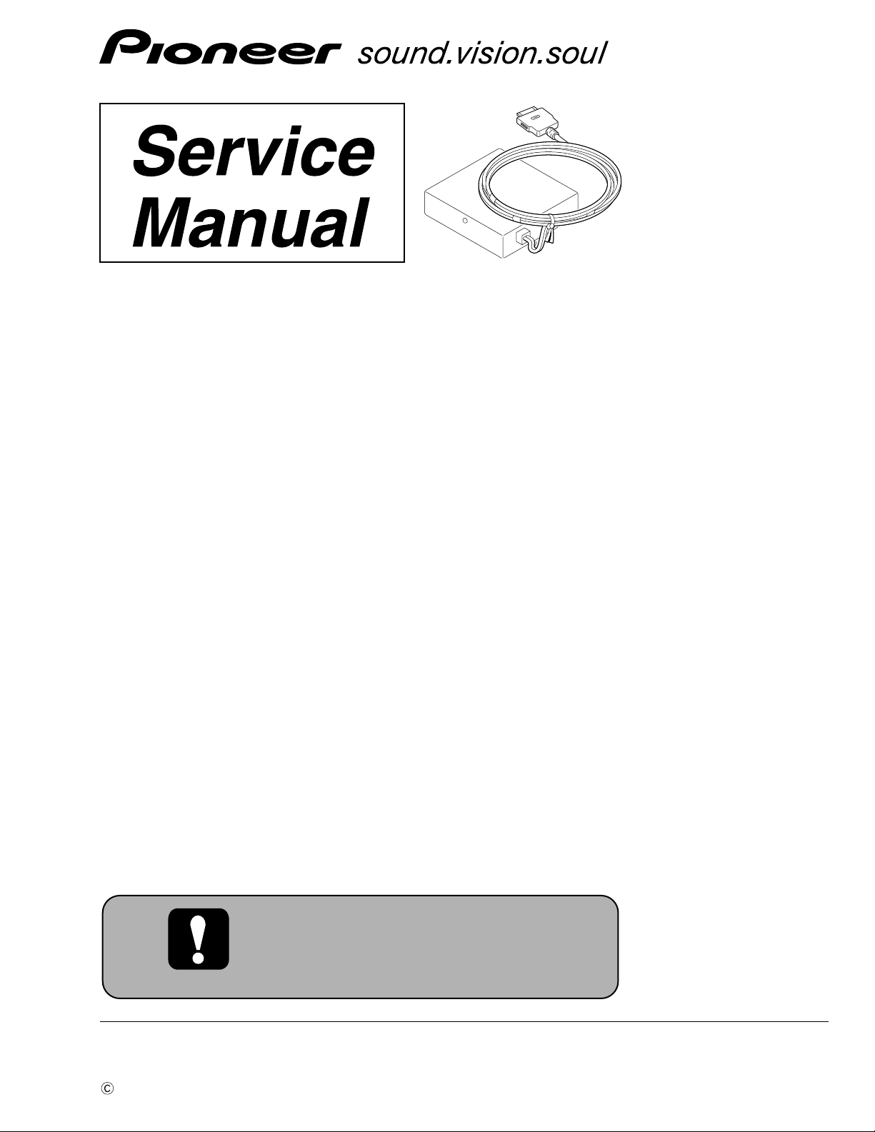
iPod
RR
ADAPTER
CD-IB100
—
/XJ/E5
For details, refer to "Important Check Points for Good Servicing".
PIONEER CORPORATION 4-1, Meguro 1-chome, Meguro-ku, Tokyo 153-8654, Japan
PIONEER ELECTRONICS (USA) INC. P.O. Box 1760, Long Beach, CA 90801-1760, U.S.A.
PIONEER EUROPE NV Haven 1087, Keetberglaan 1, 9120 Melsele, Belgium
PIONEER ELECTRONICS ASIACENTRE PTE. LTD. 253 Alexandra Road, #04-01, Singapore 159936
PIONEER CORPORATION 2006
K-ZZD. FEB. 2006 Printed in Japan
Page 2

1234
SAFETY INFORMATION
CAUTION
A
This service manual is intended for qualified service technicians; it is not meant for the casual do-it-yourselfer.
Qualified technicians have the necessary test equipment and tools, and have been trained to properly and safely repair
complex products such as those covered by this manual.
Improperly performed repairs can adversely affect the safety and reliability of the product and may void the warranty.
If you are not qualified to perform the repair of this product properly and safely, you should not risk trying to do so
and refer the repair to a qualified service technician.
W
ARNING
This product contains lead in solder and certain electrical parts contain chemicals which are known to the state of
California to cause cancer, birth defects or other reproductive harm.
B
Health & Safety Code Section 25249.6 - Proposition 65
- Service Precaution
1.You should conform to the regulations governing the product (safety, radio and noise, and other regulations),
and should keep the safety during servicing by following the safety instructions described in this manual.
2. Be careful in handling ICs. Some ICs such as MOS type are so fragile that they can be damaged by
electrostatic induction.
C
D
E
F
2
1234
CD-IB100 — /XJ/E5
Page 3
5678
[Important Check Points for Good Servicing]
In this manual, procedures that must be performed during repairs are marked with the below symbol.
Please be sure to confirm and follow these procedures.
1. Product safety
Please conform to product regulations (such as safety and radiation regulations), and maintain a safe servicing environment by
following the safety instructions described in this manual.
1 Use specified parts for repair.
Use genuine parts. Be sure to use important parts for safety.
2 Do not perform modifications without proper instructions.
Please follow the specified safety methods when modification(addition/change of parts) is required due to interferences such as
radio/TV interference and foreign noise.
3 Make sure the soldering of repaired locations is properly performed.
When you solder while repairing, please be sure that there are no cold solder and other debris.
Soldering should be finished with the proper quantity. (Refer to the example)
4 Make sure the screws are tightly fastened.
Please be sure that all screws are fastened, and that there are no loose screws.
5 Make sure each connectors are correctly inserted.
Please be sure that all connectors are inserted, and that there are no imperfect insertion.
6 Make sure the wiring cables are set to their original state.
Please replace the wiring and cables to the original state after repairs.
In addition, be sure that there are no pinched wires, etc.
7 Make sure screws and soldering scraps do not remain inside the product.
Please check that neither solder debris nor screws remain inside the product.
8 There should be no semi-broken wires, scratches, melting, etc. on the coating of the power cord.
Damaged power cords may lead to fire accidents, so please be sure that there are no damages.
If you find a damaged power cord, please exchange it with a suitable one.
9 There should be no spark traces or similar marks on the power plug.
When spark traces or similar marks are found on the power supply plug, please check the connection and advise on secure
connections and suitable usage. Please exchange the power cord if necessary.
0 Safe environment should be secured during servicing.
When you perform repairs, please pay attention to static electricity, furniture, household articles, etc. in order to prevent injuries.
Please pay attention to your surroundings and repair safely.
A
B
C
D
2. Adjustments
To keep the original performance of the products, optimum adjustments and confirmation of characteristics within specification.
Adjustments should be performed in accordance with the procedures/instructions described in this manual.
3. Lubricants, Glues, and Replacement parts
Use grease and adhesives that are equal to the specified substance.
Make sure the proper amount is applied.
4. Cleaning
For parts that require cleaning, such as optical pickups, tape deck heads, lenses and mirrors used in projection monitors, proper
cleaning should be performed to restore their performances.
5. Shipping mode and Shipping screws
To protect products from damages or failures during transit, the shipping mode should be set or the shipping screws should be
installed before shipment. Please be sure to follow this method especially if it is specified in this manual.
56
CD-IB100 — /XJ/E5
E
F
7
8
3
Page 4

1234
CONTENTS
SAFETY INFORMATION..................................................................................................................................... 2
1. SPECIFICATIONS ............................................................................................................................................ 5
2. EXPLODED VIEWS AND PARTS LIST ............................................................................................................ 6
A
B
2.1 PACKING ................................................................................................................................................... 6
2.2 EXTERIOR................................................................................................................................................. 8
3. SCHEMATIC DIAGRAM ................................................................................................................................. 10
3.1 SCHEMATIC DIAGRAM(GUIDE PAGE) .................................................................................................. 10
4. PCB CONNECTION DIAGRAM ..................................................................................................................... 16
4.1 MAIN PWB UNIT...................................................................................................................................... 16
5. ELECTRICAL PARTS LIST ............................................................................................................................ 18
6. ADJUSTMENT ............................................................................................................................................... 20
6.1 TEST MODE ............................................................................................................................................ 20
7. GENERAL INFORMATION ............................................................................................................................. 22
7.1 DIAGNOSIS ............................................................................................................................................. 22
7.1.1 DISASSEMBLY ..................................................................................................................................... 22
7.1.2 CONNECTOR FUNCTION DESCRIPTION.......................................................................................... 23
7.2 IC ............................................................................................................................................................. 24
8. OPERATIONS ................................................................................................................................................ 26
C
D
E
F
4
1234
CD-IB100 — /XJ/E5
Page 5
5678
1. SPECIFICATIONS
A
B
C
D
E
56
CD-IB100 — /XJ/E5
F
7
8
5
Page 6
N
1234
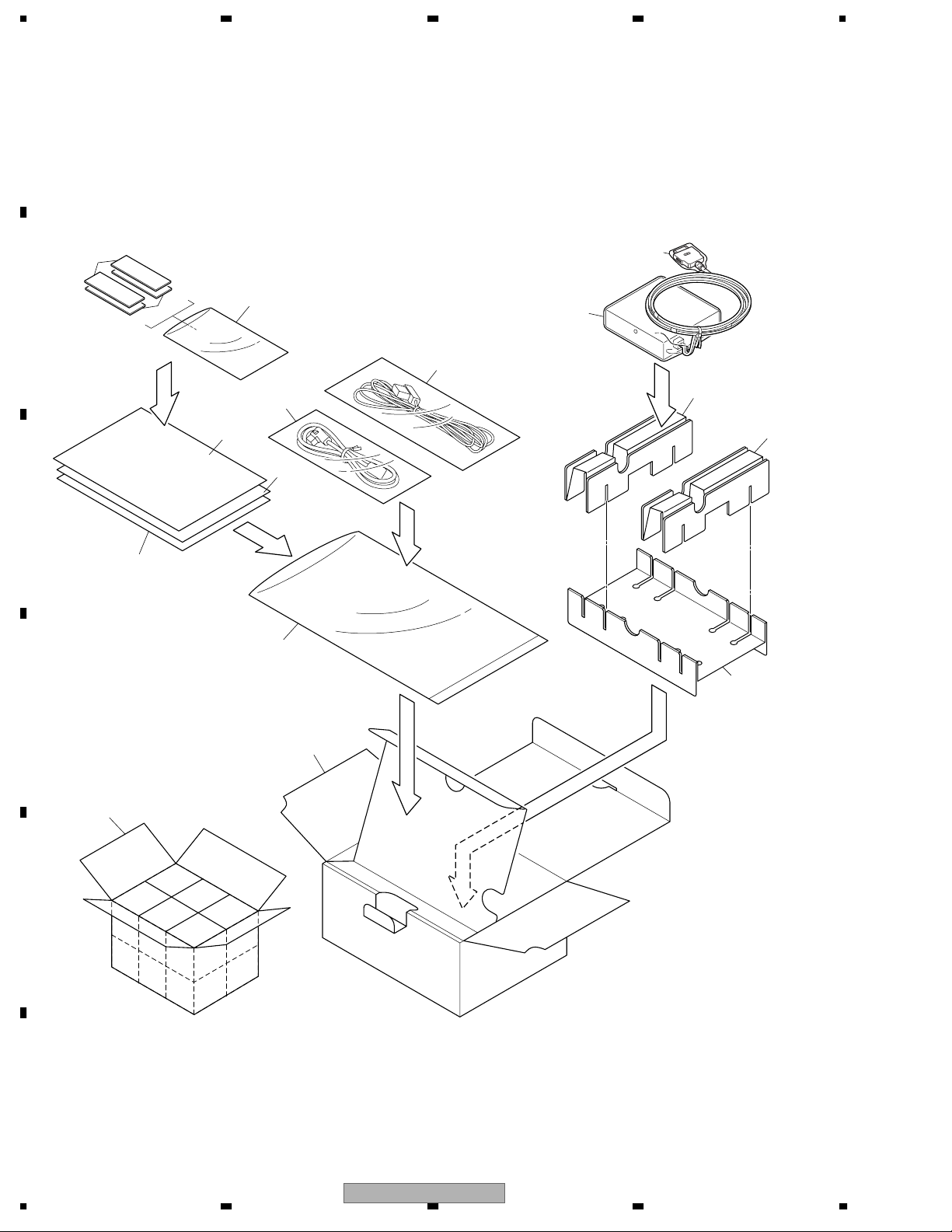
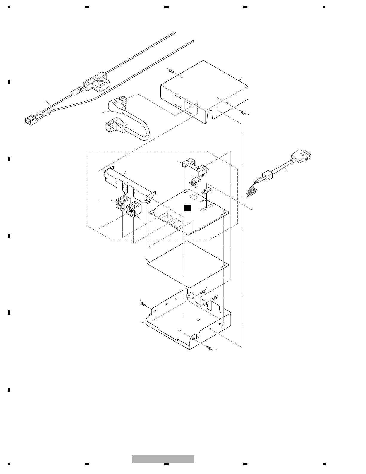
2. EXPLODED VIEWS AND PARTS LIST
OTES : • Parts marked by " * " are generally unavailable because they are not in our Master Spare Parts List.
• The > mark found on some component parts indicates the importance of the safety factor of the part.
A
Therefore, when replacing, be sure to use parts of identical designation.
• Screw adjacent to mark on the product are used for disassembly.
• For the applying amount of lubricants or glue, follow the instructions in this manual.
(In the case of no amount instructions,apply as you think it appropriate.)
2.1 PACKING
"
12
15
13
1
5
6
7
9
B
C
11
8
14
2
2
3
D
4
10
E
F
6
1234
CD-IB100 — /XJ/E5
Page 7
5678
PACKING SECTION PARTS LIST
Mark No. Description Part No.
1 Protect Bag CZE2966
2 Spacer(S) CZH6631
3 Spacer(L) CZH6632
* 4 Carton CZH6650
5 DC Cord Assy(ES) CZD2993
6 BUS Cord Assy CZD2995
7 Owner's Manual CZR2997
8 Owner's Manual CZR2998
Owner's Manual
Mark No. Description Part No.
9 Polyethylene Bag CZE2962
* 10 Contain Box CZH6651
* 11 Velcro Fastener(Hard) CZE2964
* 12 Velcro Fastener(Soft) CZE2965
* 13 Polyethylene Bag CZE2967
* 14 Polyethylene Bag CZE2970
* 15 Caution Card CRP1332
A
Part No. Language
CZR2997 English, Spanish, German, French, Italian
CZR2998 Dutch, Portuguese(B), Traditional Chinese, Arabic
B
C
D
56
CD-IB100 — /XJ/E5
E
F
7
8
7
Page 8
1234
2.2 EXTERIOR
A
2
1
14
B
7
C
3
13
12
8
11
10
1
4
A
9
6
D
1
1
1
5
E
F
8
1234
CD-IB100 — /XJ/E5
1
Page 9

5678
EXTERIOR SECTION PARTS LIST
Mark No. Description Part No.
1 Screw BSZ26P060FTB
2 DC Cord Assy(ES) CZD2993
3 BUS Cord Assy CZD2995
4 Cord Assy CZD5510
5 Chassis(Bottom) CZN6966
6 Insulator CZN6969
7 Main PWB Unit CZW5563
8 Plug(CN1) CZK2960
9 Connector(CN4) CKS3409
10 Connector(CN3) CKS3414
A
11 Connector(CN2) CKS4833
12 Holder(BUS) CZN6967
13 Holder(Power Supply) CZN6968
14 Chassis(Top) CZN8341
B
C
D
56
CD-IB100 — /XJ/E5
E
F
7
8
9
Page 10

1234
3. SCHEMATIC DIAGRAM
3.1 SCHEMATIC DIAGRAM(GUIDE PAGE)
A
Note: When ordering service parts, be sure to refer to " EXPLODED VIEWS AND PARTS LIST" or
"ELECTRICAL PARTS LIST".
Large size
A-b
A-b
SCH diagram
Guide page
Detailed page
I-POD
ACC ID
I-POD:+1.35dBs
A-a A-b
A-a
A-a
B
A-a
F/W POWER
I-POD ISOR
C
PSENSG
D
E
PSENS
3.3V 5V
5V 3.3V
SYSTEM CONTROLLER
F
A
10
1234
CD-IB100 — /XJ/E5
Page 11

5678
A
A-b
MAIN PWB UNIT
A
CD-CH ISOR
SW AMP
ASENS
MUTE
CD-CH
IP-BUS:+2.00dBs
IP-BUS IN
IP-BUS:+2.21dBs
I-POD:+2.21dBs
IP-BUS OUT
B
C
D
8.1V
BSENS
5.0V
The > mark found on some component parts indicates
the importance of the safety factor of the part.
Therefore, when replacing, be sure to use parts of
identical designation.
CD-IB100 — /XJ/E5
530µH
56
BU
E
>
F
A
7
8
11
Page 12

1234
A
B
C
A-b
1 2
I-POD ISOR
5V 3.3V
A-b
A-a
A-a
F/W POWER
D
3.3V 5V
PSENS
E
ACC ID
I-POD:+1.35dBs
PSENSG
F
A-a
12
I-POD
CD-IB100 — /XJ/E5
1234
Page 13

5678
SYSTEM CONTROLLER
3
A
A-b
B
C
A-b
A-a
A-a
D
E
56
CD-IB100 — /XJ/E5
F
A-a
7
8
13
Page 14

1234
A
IP-BUS IN
I-POD:+2.21dBs
IP-BUS:+2.21dBs
IP-BUS:+2.00dBs
B
CD-CH
IP-BUS OUT
MAIN PWB UNIT
A
C
A-b
A-a
CD-CH ISOR
MUTE
D
E
F
A-b
14
ASENS
SW AMP
1 2
CD-IB100 — /XJ/E5
1234
Page 15

5678
A
BU
>
B
530 H
C
A-b
A-a
D
ASENS
5.0V
8.1V
BSENS
3
CD-IB100 — /XJ/E5
56
The > mark found on some component parts indicates
the importance of the safety factor of the part.
Therefore, when replacing, be sure to use parts of
identical designation.
E
F
A-b
7
8
15
Page 16

1234
4. PCB CONNECTION DIAGRAM
4.1 MAIN PWB UNIT
A
NOTE FOR PCB DIAGRAMS
1.The parts mounted on this PCB
include all necessary parts for
several destination.
For further information for
respective destinations, be sure
to check with the schematic dia gram.
2.Viewpoint of PCB diagrams
Connector
P.C.Board
Capacitor
Chip Part
SIDE A
SIDE B
B
C
D
MAIN PWB UNIT
A
IC,Q
DC Cord Assy(ES)(Power Supply)
Cord Assy(iPod)
SIDE A
E
F
FRONT
A
16
1234
CD-IB100 — /XJ/E5
Page 17

5678
A
MAIN PWB UNIT
A
IC,Q
SIDE B
B
C
D
56
CD-IB100 — /XJ/E5
E
F
A
7
8
17
Page 18

N
1234
5. ELECTRICAL PARTS LIST
OTE:
A
• Parts whose parts numbers are omitted are subject to being not supplied.
• The part numbers shown below indicate chip components.
Chip Resistor
RS1/_S___J,RS1/__S___J
Chip Capacitor (except for CQS.....)
CKS....., CCS....., CSZS.....
• The > mark found on some component parts indicates the importance of the safety factor of the part.
Therefore, when replacing, be sure to use parts of identical designation.
• Meaning of the figures and others in the parentheses in the parts list.
B
Example) IC 301 is on the point (face A, 91 of x-axis, and 111 of y-axis) of the corresponding
PC board.
IC 301 (A, 91, 111) IC NJM2068V
Circuit Symbol and No. Part No.
Unit Number : CZW5563
Unit Name : Main PWB Unit
C
A
Unit Number : CZW5563
Unit Name : Main PWB Unit
MISCELLANEOUS
IC 1 IC BA3131FS
IC 2 IC TA2050FS1
IC 3 IC HA12241FP
IC 4 IC PE5483B
IC 5 IC TC7SET08FUS1
D
IC 6 IC TC7SH08FUS1
IC 7 IC PST3433UL
IC 9 IC TA2050FS1
Q1 Tr ansistor IMH3A
Q2 Tr ansistor DTA114EU
Q3 Tr ansistor DTC124EUA
Q4 Tr ansistor 2SD1767
Q5 Tr ansistor 2SC2412K
Q6 Tr ansistor 2SA1162
Q7 Tr ansistor DTC144EU
Q8 Tr ansistor DTC144EK
E
Q9 Tr ansistor 2SD1767
Q10Transistor DTC124EUA
Q11Transistor DTA114EU
Q15Transistor DTC124EUA
Q18Transistor 2SA2060
Q19Transistor 2SA1162
Q20Transistor DTC124EUA
Q23Transistor DTC114EUA
Q25Transistor 2SC4081
Q27Transistor 2SA2060
Q28Transistor DTA114EU
F
Q29Transistor DTC124EUA
D1 Diode 1SR154-400
D2 Diode HZS6L(B1)
18
1234
Circuit Symbol and No. Part No.
D3 Diode HZS7L(C2)
D4 Diode 1SS355
D5 Diode HZS9L(B2)
D9 Diode 1SR139-400
D14 Diode HZM6.2ZMWA
D29 Diode HZM6.2ZMWA
D30 Diode HZS22L(1)
L1 Choke Coil 530 µH CTH1282
L2 Inductor CZT2935
X1 Radiator 12.58 MHz CSS1601
RESISTORS
R1 RS1/16S222J
R3 RS1/16S124J
R4 RS1/16S124J
R5 RS1/16S181J
R6 RS1/16S181J
R7 RS1/16S223J
R8 RS1/16S223J
R9 RS1/16S102J
R10 RS1/16S102J
R11 RS1/16S223J
R12 RS1/16S223J
R13 RS1/16S473J
R14 RS1/16S473J
R15 RS1/16S473J
R16 RS1/16S562J
R17 RS1/16S123J
R18 RS1/16S912J
R19 RS1/16S473J
R20 RS1/16S473J
R21 RS1/16S473J
R22 RS1/16S123J
R23 RS1/16S562J
R24 RS1/16S473J
R25 RS1/16S821J
R26 RS1/16S821J
R27 RS1/16S101J
R28 RS1/16S101J
R29 RS1/16S103J
CD-IB100 — /XJ/E5
Page 19

5678
Circuit Symbol and No. Part No.
R30 RS1/16S333J
R31 RS1/16S102J
R32 RS1/16S103J
R34 RS1/16S912J
R35 RS1/16S473J
R36 RS1/16S104J
R37 RS1/16S473J
R38 RS1/16S473J
R39 RS1/16S103J
R44 RS1/16S222J
R45 RS1/16S821J
R47 RS1/16S101J
R48 RS1/16S104J
R49 RS1/16S122J
R51 RS1/16S103J
R52 BPR26CR47J
R54 RS1/16S101J
R55 RS1/16S104J
R56 RS1/16S103J
R58 RS1/16S473J
R59 RS1/16S473J
R60 RS1/8S102J
R61 RS1/16S103J
R62 RS1/16S473J
R63 RS1/16S103J
R64 RS1/16S473J
R65 RS1/16S473J
R66 RS1/16S104J
R67 RS1/16S472J
R72 RS1/16S514J
R73 RS1/16S393J
R74 RS1/16S102J
R75 RS1/16S102J
R76 RS1/16S102J
R77 RS1/16S102J
R80 RS1/16S103J
R82 RS1/16S102J
R83 RS1/16S103J
R88 RS1/16S102J
R89 RS1/16S102J
R91 RS1/16S102J
R94 RS1/16S473J
R97 RS1/16S222J
R98 RS1/16S124J
R99 RS1/16S103J
R 100 RS1/16S223J
R 101 RS1/16S223J
R 103 RS1/8S102J
R 106 RS1/16S103J
R 107 RS1/10S220J
R 108 RS1/10S220J
R 110 RS1/16S472J
R 111 RS1/16S472J
R 112 RS1/16S104J
R 113 RS1/16S104J
R 115 RS1/8S102J
R 116 RS1/8S102J
R 117 RS1/16S222J
R 118 RS1/16S103J
Circuit Symbol and No. Part No.
CAPACITORS
C1 1 000 µF/16 V CCH1234
C2 470 µF/16 V CCH1080
C3 CEAT101M16
C4 CKSRYB103K50
C7 CKSRYB104K50
C8 1 µF/50 V CCH1501
C9 1 µF/50 V CCH1501
C101 µF/50 V CCH1501
C111 µF/50 V CCH1501
C12 CEALNP100M10
C13 CEALNP100M10
C14 CEJQ220M16
C15 CEJQ220M16
C16 CEJQ220M16
C17 CEAT101M16
C18 CEAT470M10
C19 CEALNP100M10
C20 CEALNP100M10
C21 CEJQ470M6R3
C22 CKSRYB103K50
C23 CKSRYB102K50
C24 CKSRYB102K50
C25 CEAL470M6R3
C26 CKSRYB103K50
C27 CKSRYB104K50
C28 CEAL470M6R3
C30 10 µF/16 V CZC2660
C31 10 µF/16 V CZC2660
C32 CKSRYB104K50
C33 CEAT101M16
C35 CKSRYB103K50
C39 CKSRYB103K50
C411 µF/50 V CCH1501
C42 CKSQYB104K50
C43 CKSRYB104K50
C44 CKSRYB104K50
C47 CKSRYB104K50
C48 CKSRYB104K50
C49 CKSRYB104K50
C50 CKSRYB104K50
C51 CKSRYB104K50
C52 CKSRYB104K50
C53 CCSRCH102J50
C54 CCSRCH102J50
C59 CEAL4R7M25
C60 CEAL4R7M25
C61 CEAL4R7M25
C62 CEAL4R7M25
C63 CEAL220M10
C64 CEAL220M10
C70 CKSRYB104K50
C71 CKSRYB104K50
C72 CEAT101M16
C73 CKSRYB103K50
A
B
C
D
E
F
56
CD-IB100 — /XJ/E5
7
8
19
Page 20

1234
6. ADJUSTMENT
6.1 TEST MODE
A
B
Test mode
Test mode is the special mode used for the check of the failure state of an iPod adapter, or isolation of failure with iPod.
-Test mode function
(1) Check of communication between an iPod adapter and a main unit
(2) Check of charge function
(3) Change of test mode cancellation trigger
(4) Check of voice line of an iPod adapter (iPod is required)
<How to enter in the test mode>
By putting a main unit into the test mode, an iPod adapter also enters in the test mode operation.
(The way to enter in the test mode is according to the specification of a main unit.)
Example) In the case of DEH-P6700MP/XN/UC (IP-BUS model) pressing 4 + 6 Key simultaneously Reset
<How to cancel the test mode >
AccOFF/RESET (main unit) cancels the test mode.
Connect an iPod adapter to a main unit and enter in the test mode.
(1) Check of communication between an iPod adapter and a main unit
C
When switching source of a main unit to EXT (iPod), the following displays appear.
- It is possible to check whether communication between an iPod adapter and a IP-BUS is normal.
- It is possible to identify which one of "unexpected connection" or "expected connection" the model is in the
state of a display.
Display at the time of unexpected connection
i P o d - - 0 0 These 8 figures are displayed.
Display at the time of expected connection
* * * * * * 0 0 is displayed.
D
Note * portion may change with models and may be blank.
(2) Check of charge function
When pressing 1 key of 1 - 6 keys of a main unit, it is possible to turn ON/OFF of a charge circuit of the iPod adapter.
By checking ON/OFF of the No. 1 pin of a DOCK connector at the iPod adapter side and a backup power supply in
the No. 11 or 12 pin at an iPod side, it is possible to check whether the charge circuit system is running normally.
Since the state of charging is displayed if an iPod is connected, it is also possible to check whether charging is performed
normally.
Display sample (in the case of an unexpected connection unit).
E
i P o d - - 0 0 Charge circuit OFF
i P o d - - 1 0 Charge circuit ON
(3) Change of test mode cancellation trigger
When pressing 2 key of 1 - 6 keys of a main unit, it is possible to change the cancellation trigger in test mode to either
AccOFF or RESET.
Display sample (in the case of an expected connection)
* * * * * * 0 0 Cancellation trigger Acc OFF
F
* * * * * * 0 1 Cancellation trigger RESET
Although it is not usually used in the service, if setting up accidentally, cancel it by Backup OFF.
20
1234
CD-IB100 — /XJ/E5
Page 21

5678
(4) Check of voice line of an iPod adapter (iPod is required)
Usually, when iPod is connected, it becomes impossible to use the key of iPod except RESET, but if it enters in this mode,
it is possible to operate the other keys.
- An iPod adapter does not check whether the iPod has been connected, and it is possible to operate on an IP-BUS.
- Since communication with an iPod is not performed, a logo (pioneer) is not displayed on the iPod.
Since it is possible to produce a sound by playing an iPod, when the sound of the iPod does not come out from a main unit,
it shows that the iPod is out of order.
In the normal mode, since communication of data and charging are performed, a logo (pioneer) and "now charging" are
displayed in the window of the iPod.
By checking whether the keys of an iPod are operatable or not, it is possible to see if it is normal or not.
A
B
C
D
E
56
CD-IB100 — /XJ/E5
F
7
8
21
Page 22

1234
7. GENERAL INFORMATION
7.1 DIAGNOSIS
7.1.1 DISASSEMBLY
A
- Removing the Chassis (Fig.1)
1
Remove the two screws and then
remove the Chassis.
B
Chassis(Top)
1
—
1
NOTE : The Chassis(Top) may appear slightly different to photo shown above.
C
- Removing the Main PWB Unit (Fig.2)
2
1
Straighten the tab at location indicated.
2
Remove the four screws and then remove
the Main PWB Unit.
D
2
E
2
1
Main PWB Unit
Fig.1
2
Fig.2
F
22
1234
CD-IB100 — /XJ/E5
Page 23

5678
7.1.2 CONNECTOR FUNCTION DESCRIPTION
A
B
10
11
7
9
8
4
6
3
2
5
1
11P CONNECTOR IP-BUS BLUE
1
BUS +
2
BUSG1
3
BUSG1
4
NC
5
BUS -
6
BUSG1
7
BUSL1
8
ASENS
9
BUSR1
10
BUSR2
11
BUSL2
6
5
1
2
3
7
4
8
9
10
11
11P CONNECTOR IP-BUS BLACK
BUS +
1
BUSG5
2
BUSG5
3
NC
4
BUS -
5
BUSG5
6
BUSL3
7
ASENS
8
BUSR3
9
BUSAG1
10
BUSAG1
11
PIN 30
PIN 1
CORD ASSY CONNECTOR
F/W GND
1
2
F/W GND
3
-
4
-
5
-
6
-
7
-
8
-
9
-
10
ACC-IDENTIFY
F/W PWR
11
12
F/W PWR
ACC PW
13
14
-
ACC-DETECT
15
16
ACC-DETECT
-
17
DOCK TX
18
DOCK RX
19
ACC-DETECT
20
21
-
22
-
23
-
24
-
25
-
26
-
AUDIO L
27
28
AUDIO R
29
AUDIO GND
30
SGND
1
3
2
DC CONNECTOR
GND
1
-
2
B.U
3
C
D
E
56
CD-IB100 — /XJ/E5
F
7
8
23
Page 24

1234
)
o.
e
n
CNot used
3RO
t
pp
7.2 IC
Pin Functions (PE5483B
A
1,2N
4-10 NC Not used
11 reset I Chip reset input
12,13 NC Not used
14 VSS GND
15 X2 Crystal connection for system clock oscillation
16 X1 I Crystal connection for system clock oscillation
17 REGOFF Regulator operation specification signal
18 REGC Capacity connection for regulator output stability
19 VDD Power supply
Pin N
20 MODEL I Model select input
B
21 SYSPW O System power control output
22 DALMON O System operation situation output
23 NC Not used
24 IPPW O Driver power control output
25 IPSELECT O Selector switch output
26 PID O Communication mode (UART) notification output
27 NC Not used
28 MUTE O Mute output
29-37 NC Not used
38 psensg I Connection sense input
39 TESTIN I Chip test input
40 VSS GND
C
41 VDD Power supply
42,43 NC Not used
44 PPOWER O Power control output
45-64 NC Not used
65 TESTSCK O Serial clock output
66 TESTSI I Serial data input
67 TESTO O Serial data output
68-72 NC Not used
73 IC I GND
74-81 NC Not used
82 AVDD Power supply for A/D converter
83 AVREF1 Standard voltage for A/D converter
D
84 AVSS GND for A/D converter
85 RX I Data input (IE-BUS)
86 TX O Data output (IE-BUS)
87 nmi I NMI input
88,89 NC Not used
90 psens I Connection sense input
91 NC Not used
92 asens I ACC sense input
93 bsens I Backup sense input
94 NC Not used
95 RXIPOD I Serial data input
E
96 TXIPOD O Serial data output
97-100 NC Not used
PE5483B
81
80
Pin Nam
I/O Function and Operatio
MDATA I/O ROM data input / outpu
51
50
F
100
24
31
1
1234
30
CD-IB100 — /XJ/E5
Page 25

5678
PST3433UL
VOUT
VDD
TA2050FS1
1
2
NC
Vref
IN1(-)
NC
13 9101112141516
4 VSS
3 NC
IN1(+)
IN2(+)
TC7SET08FUS1,TC7SH08FUS1
IN B
IN A
GND
NC
IN2(-)
1
2
3
NC
A
5 VCC
B
4 OUT Y
C
HA12241FP
+
24 876513
OUT1
VREF
BIAS
VREF
NC
VCCstb
GND
+
-
RECEIVER
OUTPUT
NC
VCC
+BUS
DRIVER
OUTPUT
(current)
COM
NC
+
-
+
D
OUT2
-BUS
5678
E
132
4
S1 R out S2 GND
56
CD-IB100—/XJ/E5
F
7
8
25
Page 26

1234
8. OPERATIONS
A
B
C
D
E
F
26
1234
CD-IB100—/XJ/E5
Page 27

5678
A
B
C
D
E
56
CD-IB100—/XJ/E5
F
7
8
27
Page 28

1234
A
B
C
D
E
F
28
1234
CD-IB100—/XJ/E5
 Loading...