

Page 1
PIONEER CORPORATION 4-1, Meguro 1-chome, Meguro-ku, Tokyo 153-8654, Japan
PIONEER ELECTRONICS (USA) INC. P.O. Box 1760, Long Beach, CA 90801-1760, U.S.A.
PIONEER EUROPE NV Haven 1087, Keetberglaan 1, 9120 Melsele, Belgium
PIONEER ELECTRONICS ASIACENTRE PTE. LTD. 253 Alexandra Road, #04-01, Singapore 159936
PIONEER CORPORATION 2002
PDP-503PC
PLASMA DISPLAY
PDP-503PC
THIS MANUAL IS APPLICABLE TO THE FOLLOWING MODEL(S) AND TYPE(S).
Model Type Power Requirement Remarks
PDP-503PC TAXQ AC110 - 240V
This service manual should be used together with the following manual(s).
Model No. Order No. Remarks
PDP-503PC ARP3135 SCHEMATIC DIAGRAM and PCB DIAGRAM
ORDER NO.
ARP3134
This product is component of system.
Component System Service Manual Remarks
Plasma Display System PDP-503HDC Media Receiver PDP-R03C ARP3132
Plasma Display PDP-503PC ARP3134 This Service Manual
For details, refer to "Important symbols for good services" on the next page.
ARP3135
T-ZZY SEPT. 2002 printed in Japan
Page 2

1234
SAFETY INFORMATION
A
This service manual is intended for qualified service technicians ; it is not meant for the casual
do-it-yourselfer. Qualified technicians have the necessary test equipment and tools, and have been
trained to properly and safely repair complex products such as those covered by this manual.
Improperly performed repairs can adversely affect the safety and reliability of the product and may
void the warranty. If you are not qualified to perform the repair of this product properly and safely,
you should not risk trying to do so and refer the repair to a qualified service technician.
WARNING
This product contains lead in solder and certain electrical parts contain chemicals which are known to the state of California to
cause cancer, birth defects or other reproductive harm.
B
NOTICE
(FOR CANADIAN MODEL ONLY)
Fuse symbols (fast operating fuse) and/or (slow operating fuse) on PCB indicate that replacement parts
must be of identical designation.
REMARQUE
(POUR MODÈLE CANADIEN SEULEMENT)
Les symboles de fusible (fusible de type rapide) et/ou (fusible de type lent) sur CCI indiquent que les pièces
de remplacement doivent avoir la même désignation.
C
Health & Safety Code Section 25249.6 - Proposition 65
SAFETY PRECAUTIONS
NOTICE : Comply with all cautions and safety related notes
located on or inside the cabinet and on the chassis.
The following precautions should be observed :
1. When service is required, even though the PDP UNIT an
isolation transformer should be inserted between the power line
and the set in safety before any service is performed.
D
2. When replacing a chassis in the set, all the protective devices
must be put back in place, such as barriers, nonmetallic knobs,
adjustment and compartment covershields, isolation resistorcapacitor, etc.
3. When service is required, observe the original lead dress. Extra
precaution should be taken to assure correct lead dress in the
high voltage circuitry area.
4. Always use the manufacture's replacement components.
Especially critical components as indicated on the circuit
diagram should not be replaced by other manufacture's.
Furthermore where a short circuit has occurred, replace those
E
components that indicate evidence of overheating.
5. Before returning a serviced set to the customer, the service
technician must thoroughly test the unit to be certain that it is
completely safe to operate without danger of electrical shock,
and be sure that no protective device built into the set by the
manufacture has become defective, or inadvertently defeated
during servicing. Therefore, the following checks should be
performed for the continued protection of the customer and
servicetechnician.
6. Perform the following precautions against unwanted radiation
and rise in internal temperature.
• Always return the internal wiring to the original styling.
• Attach parts (Gascket, Ferrite Core, Ground, Rear Cover,
Shield Case etc.) surely after disassembly.
7. Perform the following precautions for the PDP panel.
• When the front case is removed, make sure nothing hits the
panel face, panel corner, and panel edge (so that the glass does
not break).
• Make sure that the panel vent does not break. (Check that the
cover is attached.)
• Handle the FPC connected to the panel carefully.
Twisting or pulling the FPC when connecting it to the
connector will cause it to peel off from the panel.
8. Pay attention to the following.
• When the front case is removed, infrared ray is radiated and
may disturb reception of the remote control unit.
• Pay extreme caution when the front case and rear panel are
removed because this may cause a high risk of disturbance to
TVs and radios in the surrounding.
F
2
1234
PDP-503PC
Page 3

5678
Leakage Current Cold Check
With the AC plug removed from an AC power source, place a
jumper across the two plug prongs. Turn the AC power switch on.
Using an insulation tester (DC 500V), connect one lead to the
jumpered AC plug and touch the other lead to each exposed metal
part (input/output terminals, screwheads, metal overlays, control
shafts, etc.), particularly any exposed metal part having a return
path to the chassis. Exposed metal parts having a return path to
the chassis should have a minimum resistor reading of 0.3MΩ
and a maximum resistor reading of 5MΩ. Any resistor value
below or above this range indicates an abnormality which
requires corrective action. Exposed metal parts not having a
return path to the chassis will indicate an open circuit.
Leakage Current Hot Check
Plug the AC line cord directly into an AC power source (do not
use an isolation transformer for this check).
Turn the AC power switch on.
Using a "Leakage Current Tester (Simpson Model 229
equivalent)", measure for current from all exposed metal parts of
the cabinet (input/output terminals, screwheads, metal overlays,
control shaft, etc.), particularly any exposed metal part having a
return path to the chassis, to a known earth ground (water pipe,
conduit, etc.). Any current measured must not exceed 0.5mA.
ANY MEASUREMENTS NOT WITHIN THE LIMITS
OUTLINED ABOVE ARE INDICATIVE OF A POTENTIAL
SHOCK HAZARD AND MUST BE CORRECTED BEFORE
RETURNING THE SET TO THE CUSTOMER.
PRODUCT SAFETY NOTICE
Many electrical and mechanical parts in PIONEER set have
special safety related characteristics. These are often not evident
from visual inspection nor the protection afforded by them
necessarily can be obtained by using replacement components
rated for higher voltage, wattage, etc. Replacement parts which
have these special safety characteristics are identified in this
Service Manual.
Electrical components having such features are identified by
marking with a on the schematics and on the parts list in this
Service Manual.
The use of a substitute replacement component which dose not
have the same safety characteristics as the PIONEER
recommended replacement one, shown in the parts list in this
Service Manual, may create shock, fire or other hazards.
Product Safety is continuously under review and new instructions
are issued from time to time. For the latest information, always
consult the current PIONEER Service Manual. A subscription to,
or additional copies of, PIONEER Service Manual may be
obtained at a nominal charge from PIONEER.
Leakage
current
tester
Reading should
not be above
0.5mA
Device
under
test
Test all
exposed metal
surfaces
Also test with
plug reversed
(Using AC adapter
plug as required)
Earth
ground
AC Leakage Test
A
B
C
D
E
56
PDP-503PC
F
7
8
3
Page 4
1234
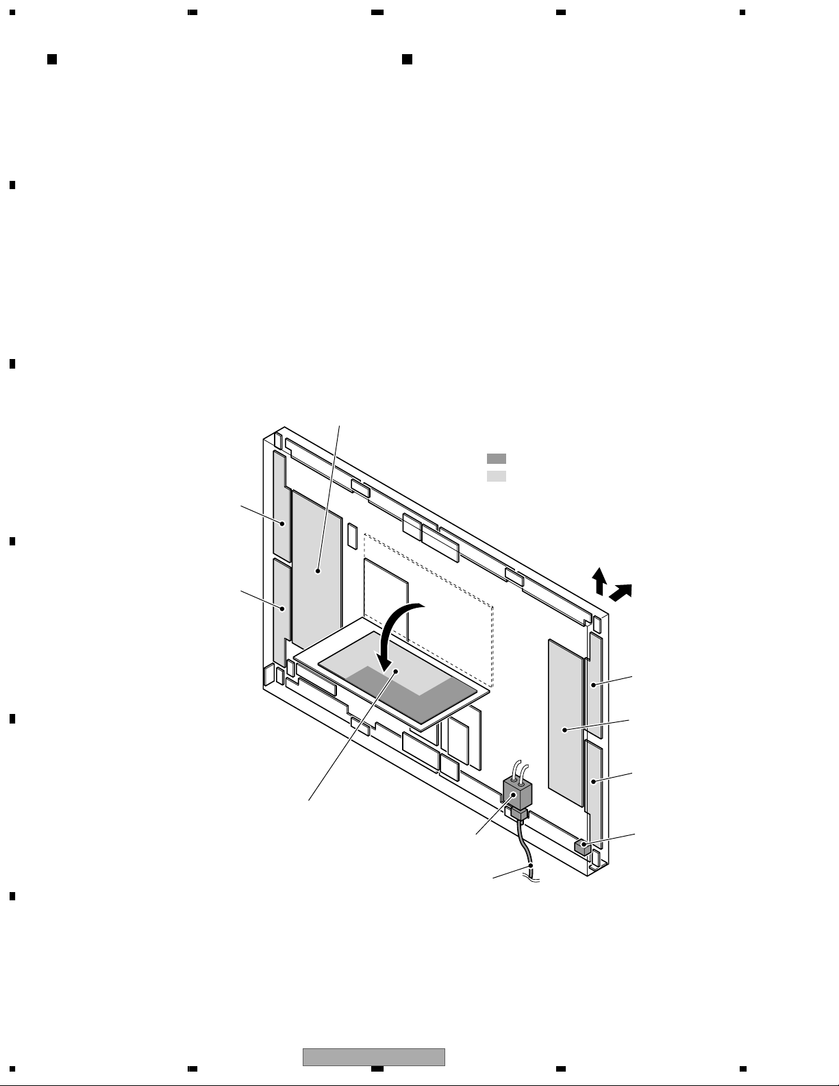
Charged Section
The places where the commercial AC power is used without
passing through the power supply transformer.
A
If the places are touched, there is a risk of electric shock. In
addition, the measuring equipment can be damaged if it is
connected to the GND of the charged section and the GND of the
non-charged section while connecting the set directly to the
commercial AC power supply. Therefore, be sure to connect the
set via an insulated transformer and supply the current.
1. AC Power Cord
2. AC Inlet with Filter
3. Power Switch (S1)
4. Fuse (In the SW POWER SUPPLY Module)
B
5. STB Transformer and Converter Transformer
(In the SW POWER SUPPLY Module)
6. Other primary side of the SW POWER SUPPLY Module
C
SCAN (A)
Assy
Y DRIVE
Assy
High Voltage Generating Point
The places where voltage is 100V or more except for the charged
places described above. If the places are touched, there is a risk of
electric shock.
1. SW POWER SUPPLY Module ...................................... (225V)
2. X DRIVE Assy ............................................... (–300V to 225V)
3. Y DRIVE Assy ................................................................ (355V)
4. SCAN (A) Assy .............................................................. (355V)
5. SCAN (B) Assy .............................................................. (355V)
6. X CONNECTOR (A) Assy ............................ (–300V to 225V)
7. X CONNECTOR (B) Assy ............................ (–300V to 225V)
: Part is Charged Section.
: Part is the High Voltage Generating Points
other than the Charged Section.
Top
SCAN (B)
Assy
D
∗ Remove the IF Earth Metal (No.14 on the page 25)
beforehand when inclines the power supply unit
as the right figure.
E
SW POWER SUPPLY
Module
AC Inlet with Filter
Power Cord
Front
X CONNECTOR (A)
Assy
X DRIVE
Assy
X CONNECTOR (B)
Assy
Power Switch
(S1)
Fig.1 Charged Section and High Voltage Generating Point (Rear View)
F
4
1234
PDP-503PC
Page 5

5678
[ Important symbols for good services ]
In this manual, the symbols shown-below indicate that adjustments, settings or cleaning should be made securely.
When you find the procedures bearing any of the symbols, be sure to fulfill them:
A
1. Product safety
You should conform to the regulations governing the product (safety, radio and noise, and other regulations), and
should keep the safety during servicing by following the safety instructions described in this manual.
2. Adjustments
To keep the original performances of the product, optimum adjustments or specification confirmation is indispensable.
In accordance with the procedures or instructions described in this manual, adjustments should be performed.
3. Cleaning
For optical pickups, tape-deck heads, lenses and mirrors used in projection monitors, and other parts requiring cleaning,
proper cleaning should be performed to restore their performances.
B
4. Shipping mode and shipping screws
To protect the product from damages or failures that may be caused during transit, the shipping mode should be set or
the shipping screws should be installed before shipping out in accordance with this manual, if necessary.
5. Lubricants, glues, and replacement parts
Appropriately applying grease or glue can maintain the product performances. But improper lubrication or applying
glue may lead to failures or troubles in the product. By following the instructions in this manual, be sure to apply the
prescribed grease or glue to proper portions by the appropriate amount.For replacement parts or tools, the prescribed
ones should be used.
C
D
56
PDP-503PC
E
F
7
8
5
Page 6

1234
CONTENTS
SAFETY INFORMATION..................................................................................................................................... 2
A
B
C
D
1. SPECIFICATIONS ............................................................................................................................................ 7
2. EXPLODED VIEWS AND PARTS LIST ............................................................................................................ 8
2.1 PACKING ...................................................................................................................................................8
2.2 UNDER LAYER SECTION (1) ................................................................................................................... 9
2.3 UNDER LAYER SECTION (2) ................................................................................................................. 10
2.4 UNDER LAYER SECTION (3) ................................................................................................................. 12
2.5 UNDER LAYER SECTION (4) ................................................................................................................. 14
2.6 UNDER LAYER SECTION (5) ................................................................................................................. 16
2.7 MIDDLE LAYER SECTION (1)................................................................................................................. 18
2.8 MIDDLE LAYER SECTION (2)................................................................................................................. 20
2.9 UPPER LAYER SECTION (1).................................................................................................................. 22
2.10 UPPER LAYER SECTION (2)................................................................................................................ 24
2.11 FRONT CASE SECTION....................................................................................................................... 26
2.12 REAR SECTION .................................................................................................................................... 27
2.13 PDP SERVICE ASSY 503 (AWU1068).................................................................................................. 28
2.14 PANEL CHASSIS (50) ASSY (AWU1066) ............................................................................................. 28
3. BLOCK DIAGRAM AND SCHEMATIC DIAGRAM..........................................................................................30
3.1 BLOCK DIAGRAM ................................................................................................................................... 30
3.1.1 OVERALL DIAGRAM......................................................................................................................... 30
3.1.2 MR INTERFACE ASSY ..................................................................................................................... 32
3.1.3 DIGITAL VIDEO ASSY.......................................................................................................................34
3.1.4 X DRIVE ASSY.................................................................................................................................. 35
3.1.5 Y DRIVE ASSY .................................................................................................................................. 36
3.1.6 SUB ADDRESS A and B ASSYS ...................................................................................................... 38
3.1.7 ADR RESONANCE ASSY................................................................................................................. 39
3.1.8 ADR CONNECT A, B, C and D ASSYS ............................................................................................40
3.1.9 AUDIO AMP and SP TERMINAL ASSYS.......................................................................................... 41
3.2 WAVEFORMS .......................................................................................................................................... 42
4. PCB CONNECTION DIAGRAM ..........................................................................................(Refer to ARP3135)
5. PCB PARTS LIST ........................................................................................................................................... 46
6. ADJUSTMENT ............................................................................................................................................... 56
6.1 SERVICE FACTORY MODE.................................................................................................................... 56
6.1.1 How to Enter the Service Factory Mode............................................................................................ 57
6.1.2 General Information of the Plasma Display and Media Receiver ...................................................... 58
6.1.3 Adjustment and Setting Item of the Plasma Display.......................................................................... 59
6.2 ADJUSTMENT REQUIRED WHEN THE SET IS REPAIRED OR REPLACED....................................... 62
6.3 ADJUSTMENT......................................................................................................................................... 63
6.4 COMMAND .............................................................................................................................................. 70
6.4.1 RS-232C Command ..........................................................................................................................70
6.4.2 GET Command.................................................................................................................................. 74
7. GENERAL INFORMATION............................................................................................................................. 76
7.1 DIAGNOSIS ............................................................................................................................................. 76
7.1.1 PCB LOCATION ................................................................................................................................76
7.1.2 SHUT DOWN/POWER DOWN DIAGNOSIS BY LED DISPLAY .......................................................77
7.1.3 DISASSEMBLY.................................................................................................................................. 84
7.2 IC INFORMATION.................................................................................................................................... 88
8. PANEL FACILITIES ...................................................................................................................................... 107
E
F
6
1234
PDP-503PC
Page 7
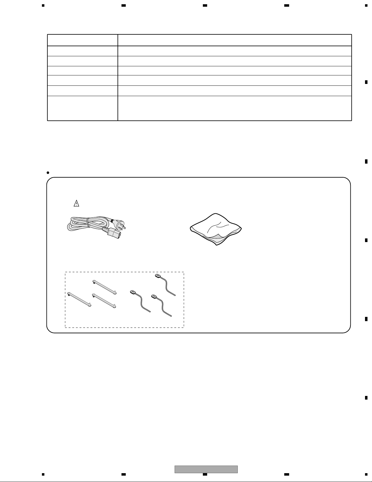
Power cord
Cleaning cloth
Three speed clamps
Three bead bands
Accessories
Binder Assy (AEC1908)
(ADG1195)
(AED1208)
• Design and specifications are subject to change without notice.
Item Model: PDP-503PC
Number of Pixels 1280 × 768 pixels
Audio Amplifier 12 W + 12 W (10% distortion)
Power Requirement AC 110–240 V, 50/60 Hz, 371 W (0.8 W Standby)
Dimensions 1218 (W) × 714 (H) × 98 (D) mm [47
31/32 (W) × 281/8 (H) × 37/8 (D) inch]
Weight 38.9 kg (85.8 lbs)
Accessories
Power Cord, Cleaning Cloth, Three speed clamps, Three bead bands
5678
1. SPECIFICATIONS
A
B
C
D
PDP-503PC
56
E
F
7
8
7
Page 8

1234
2. EXPLODED VIEWS AND PARTS LIST
NOTES:
A
2.1 PACKING
B
C
Parts marked by "NSP" are generally unavailable because they are not in our Master Spare Parts List.
The mark found on some component parts indicates the importance of the safety factor of the part.
Therefore, when replacing, be sure to use parts of identical designation.
Screws adjacent to mark on product are used for disassembly.
For the applying amount of lubricants or glue, follow the instructions in this manual.
(In the case of no amount instructions, apply as you think it appropriate.)
14
1
14
2
3
11
D
PACKING parts List
Mark No. Description Part No.
E
1 Upper Carton C AHD3155
2 Under Carton AHD3037
3 Pad AHA2280
4 Mirror Mat AHG1284
5 Caution Sheet ARM1201
8
12
10
13
9
4
6
5
3
7
2
Mark No. Description Part No.
11 Power Cord ADG1195
>
12 Ferrite Core (L4) ATX1039
13 Caution Sheet ARM1213
14 Label (Blue16) AAX2787
6 Front Sheet AHB1241
7 Cord Case AHC1037
8 Vinyl Bag AHG1310
9 Wiping Cloth AED1208
10 Binder Assy AEC1908
F
(Speed Clamp x 3, Bead Band x 3)
8
1234
PDP-503PC
Page 9
6
11
1
10
10
11
2
4
10
11
3
6
777
6
6
6
Upper side
6
8
9
9
8
6
67
6
14
5
10
1112
7
5
Refer to
"2.14 PANEL CHASSIS ASSY
(AWU1066)".
5678
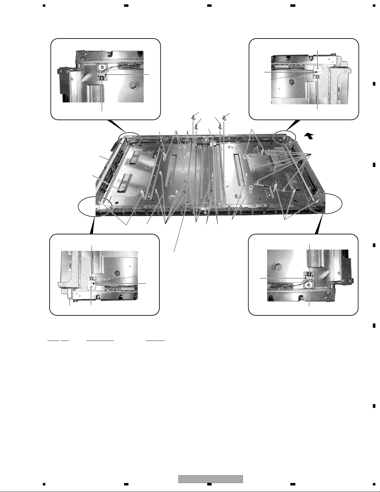
2.2 UNDER LAYER SECTION (1)
A
B
UNDER LAYER SECTION (1) parts List
Mark No. Description Part No.
1 CLAMP A Assy AWZ6738
2 CLAMP B Assy AWZ6739
3 CLAMP C Assy AWZ6740
4 CLAMP D Assy AWZ6741
NSP 5 Panel Chassis (50) Assy AWU1066
[Refer to "2.14 PANEL CHASSIS (50) ASSY".]
6 Wire Saddle AEC1904
7 Circuit Board Spacer AEC1872
8 Circuit Board Spacer AEC1873
NSP 9 PCB Support AEC1253
10 Locking Card Spacer AEC1736
11 Screw ABA1301
12 V Cushion AED1205
C
D
E
F
56
PDP-503PC
7
8
9
Page 10
1234
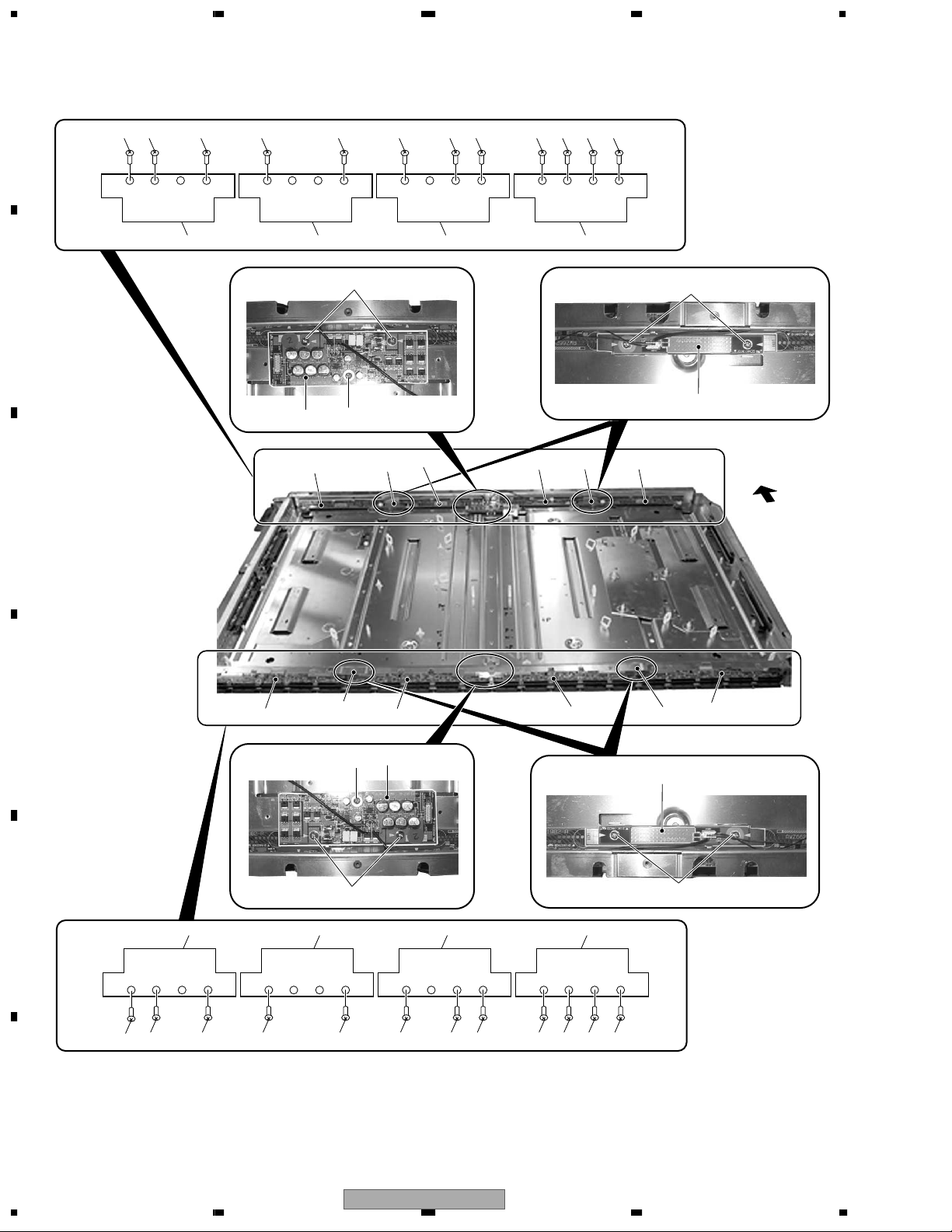
2.3 UNDER LAYER SECTION (2)
A
11 11 11 11 11 11 11 11
11
1 2 3 4
11 11 11
10
B
11
9
15
C
D
4
7
2
3
36 4
2
8
10
5 or 6
Upper side
1
9
11
10
E
11
11
F
10
1234
4
3 2 1
11 11 11
11
PDP-503PC
7 or 8
10
111111111111
Page 11

5678
UNDER LAYER SECTION (2) parts List
Mark No. Description Part No.
NSP 1 ADR CONNECT A Assy AWZ6626
NSP 2 ADR CONNECT B Assy AWZ6627
NSP 3 ADR CONNECT C Assy AWZ6628
NSP 4 ADR CONNECT D Assy AWZ6629
5 BRIDGE A Assy AWZ6734
6 BRIDGE B Assy AWZ6735
7 BRIDGE C Assy AWZ6736
8 BRIDGE D Assy AWZ6737
9 ADR RESONANCE Assy AWZ6750
10 Screw ABA1301
A
11 Screw VBB30P100FNI
B
C
D
56
PDP-503PC
E
F
7
8
11
Page 12

1234
2.4 UNDER LAYER SECTION (3)
A
Upper side
B
1
1715 16
18
3
C
28
D
E
12
1212
249
6
21
29
20
7 (Upper Side)
8 (Bottom Side)
11
14
19
13
13
28
12
25
13
29
28
23
25
3
11
510
F
12
1234
PDP-503PC
10 4
Upper side
Page 13

5678
UNDER LAYER SECTION (3) parts List
Mark No. Description Part No.
1 DIGITAL VIDEO Assy AWV1979
2• • • • •
3 X DRIVE Assy AWV1901
4 X CONNECTOR (A) Assy AWZ6732
5 X CONNECTOR (B) Assy AWZ6733
6 ADR RESONANCE Assy AWZ6750
7 SUB ADDRESS A Assy AWZ6689
8 SUB ADDRESS B Assy AWZ6690
NSP 9 Scan Heat Sink ANH1594
10 Coil Silicone Sheet AEH1048
A
11 • • • • •
12 Screw ABZ30P060FMC
13 Screw VBB30P100FNI
14 Screw PMB30P060FNI
15 J201 Flexible Flat Cable ADD1194
16 J202 Flexible Flat Cable ADD1194
17 J209 Flexible Flat Cable ADD1191
18 J204 Flexible Flat Cable ADD1196
19 J210 Flexible Flat Cable ADD1190
20 J211 Flexible Flat Cable ADD1186
21 J212 Flexible Flat Cable ADD1188
22 • • • • •
NSP 23 Drive Heatsink Assy ANH1598
24 Silicone Sheet AEH1039
25 Drive Silicone Sheet AEH1041
26 • • • • •
27 • • • • •
28 Flat Clamp AEC1879
NSP 29 Metal Fittings ANG2464
B
C
D
56
PDP-503PC
E
F
7
8
13
Page 14

1234
2.5 UNDER LAYER SECTION (4)
A
B
16
211
2
22
7
16
C
Upper side
D
8
7
15
Upper side
5
19
20
18
18
17
14
23
8
25
18
15
7
24
25
2
15
17
E
3
F
14
1234
PDP-503PC
11
10
13
10
12
4
Page 15

5678
UNDER LAYER SECTION (4) parts List
Mark No. Description Part No.
1 DIGITAL VIDEO Assy AWV1979
2 Y DRIVE Assy AWZ6707
3 SCAN (A) Assy AWZ6722
4 SCAN (B) Assy AWZ6723
5 SENSOR Assy AWZ6696
6• • • • •
7 Flat Clamp AEC1879
NSP 8 Metal Fittings ANG2464
9• • • • •
10 Coil Silicone Sheet AEH1048
A
11 Scan IC Spring (L) ABK1026
12 Scan IC Spring (R) ABK1027
13 Scan Insulation Sheet AMR3271
14 Rivet BEC1066
15 Circuit Board Spacer AEC1872
16 Screw ABZ30P060FMC
17 Screw PMB30P060FNI
18 Screw VBB30P100FNI
19 J208 Flexible Flat Cable ADD1191
20 J207 Flexible Flat Cable ADD1190
21 J203 Flexible Flat Cable ADD1184
22 J205 Flexible Flat Cable ADD1189
23 J206 Flexible Flat Cable ADD1187
NSP 24 Drive Heatsink Assy ANH1598
25 Drive Silicone Sheet AEH1041
B
C
D
56
PDP-503PC
E
F
7
8
15
Page 16
1234
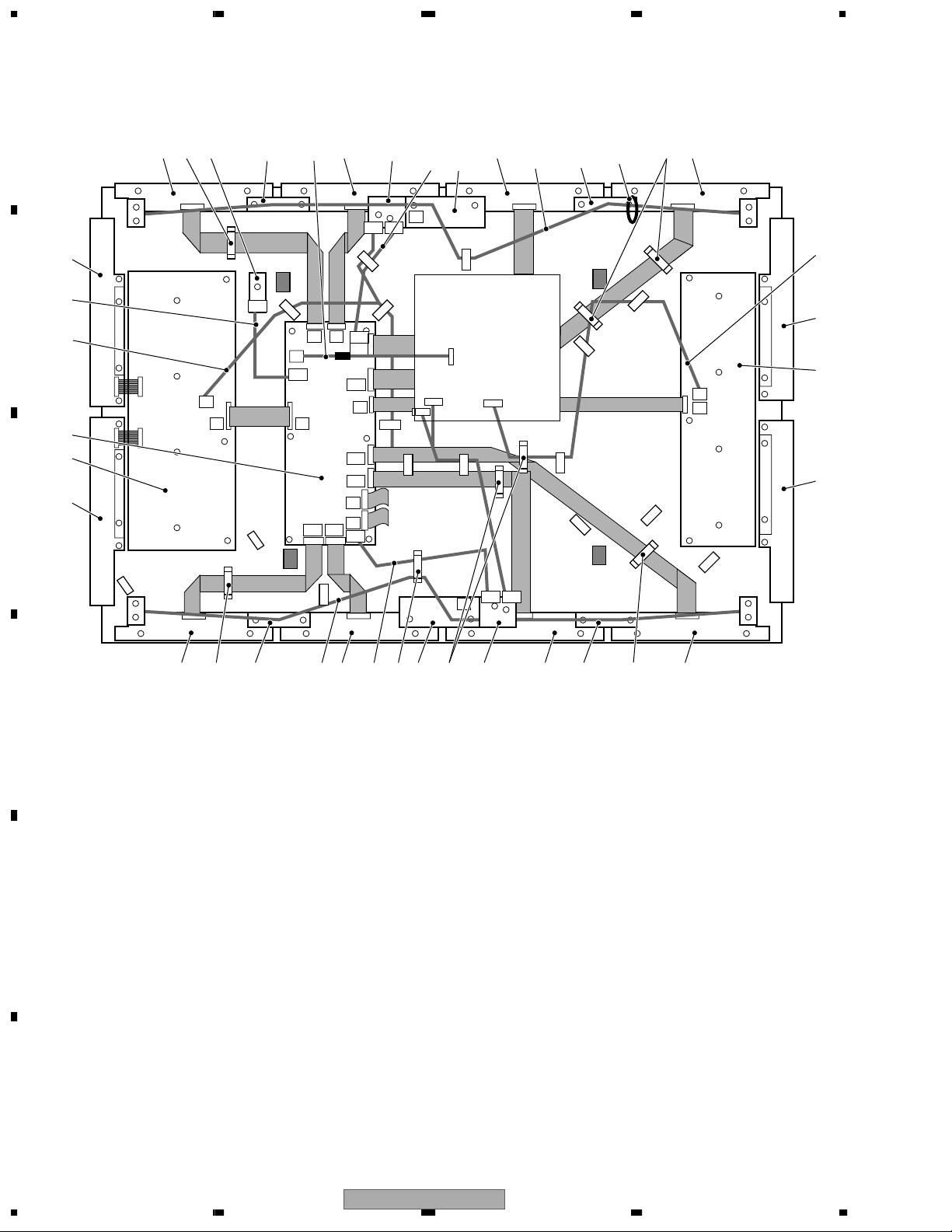
2.6 UNDER LAYER SECTION (5)
A
1 22 16
8 10
12
24
B
TE1
27
D1
D18
Y1
15
Y2
14
13
C
26
2
SA1 SA2
25
K3
3 422
5
29
9
31
28
17
D9D8
D16
D10
19
D11
D7
D6
D15
D14
D2
D3
D13D12
D17
SA2 SA1
K3
K3
X1
X2
18
1 22 22222 30 2232 3 46 75 11
D
E
F
16
1234
PDP-503PC
Page 17

5678
UNDER LAYER SECTION (5) parts List
Mark No. Description Part No.
NSP 1 ADR CONNECT A Assy AWZ6626
NSP 2 ADR CONNECT B Assy AWZ6627
NSP 3 ADR CONNECT C Assy AWZ6628
NSP 4 ADR CONNECT D Assy AWZ6629
5 ADR RESONANCE Assy AWZ6750
6 BRIDGE A Assy AWZ6734
7 BRIDGE B Assy AWZ6735
8 BRIDGE C Assy AWZ6736
9 BRIDGE D Assy AWZ6737
10 SUB ADDRESS A Assy AWZ6689
A
11 SUB ADDRESS B Assy AWZ6690
12 SCAN (A) Assy AWZ6722
13 SCAN (B) Assy AWZ6723
14 Y DRIVE Assy AWZ6707
15 DIGITAL VIDEO Assy AWV1979
16 SENSOR Assy AWZ6696
17 X CONNECTOR (A) Assy AWZ6732
18 X CONNECTOR (B) Assy AWZ6733
19 X DRIVE Assy AWV1901
20 • • • • •
21 • • • • •
22 Flat Clamp AEC1879
23 • • • • •
24 J110 3P Housing Wire ADX2704
25 J108 8P Housing Wire ADX2701
26 J101 Wire F ADX2726
27 J102 Wire E ADX2782
28 J103 13P Housing Wire ADX2700
29 J116 4P Housing SP Wire ADX2756
30 J109 Wire G ADX2743
31 Binder AEC-093
32 J117 4P Housing SP Wire ADX2756
B
C
D
56
PDP-503PC
E
F
7
8
17
Page 18
1234
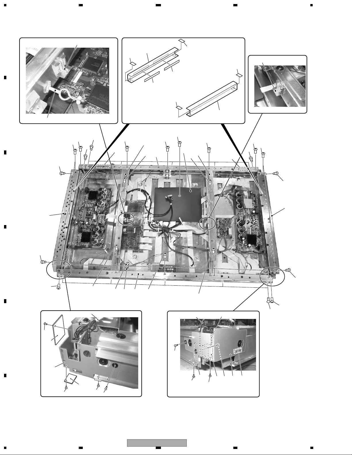
2.7 MIDDLE LAYER SECTION (1)
A
B
17
C
16
11
12
9
9
9
9
9
13
7
6
4
8
9
31
11
16
11
6
11
7
15
14
9
5
8
13
9
9
9
9
7
7
9
D
9
10
E
24
3
20
24
8
18
1
25
21
19
2726
9
21
25
22
8
10
29
2
28
24
30
23
32
12
F
18
1234
PDP-503PC
Page 19

5678
MIDDLE LAYER SECTION (1) parts List
Mark No. Description Part No.
1 IR RECEIVE (P) Assy AWZ6658
2 LED Assy AWZ6655
3 FRONT KEY CONNECT Assy AWZ6657
NSP 4 Sub Frame L ANG2455
NSP 5 Sub Frame R ANG2456
6 FPC Cushion AEB1370
NSP 7 Front Chassis V ANA1661
8 Screw AMZ30P060FZK
9 Screw ABA1294
10 Screw BMZ30P060FMC
A
11 V Cushion AED1205
NSP 12 Card Spacer AEC1902
13 Spacer B AMR3300
14 Power Sheet AMR3291
15 Rivet BEC1066
16 Card Corner Holder BEC1144
17 Niplocker BEC1136
18 J113 Wire J ADX2718
NSP 19 Front Chassis H (W) ANA1679
NSP 20 IR Holder ANG2494
21 Nyron Rivet AEC1671
22 J104 3P Housing Wire ADX2732
NSP 23 Switch Holder ANG2493
24 Screw BMZ30P040FMC
25 Screw ABZ30P050FZK
26 Ferrite Core (L6) ATX1037
27 Ferrite Core Holder AEC1818
28 Power Switch (S1) ASG1082
29 J106 Wire PC ADX2723
30 Screw BMZ30P060FZK
NSP 31 Front Chassis ANA1697
32 Gascket R ANK1695
B
C
D
56
PDP-503PC
E
F
7
8
19
Page 20
1234
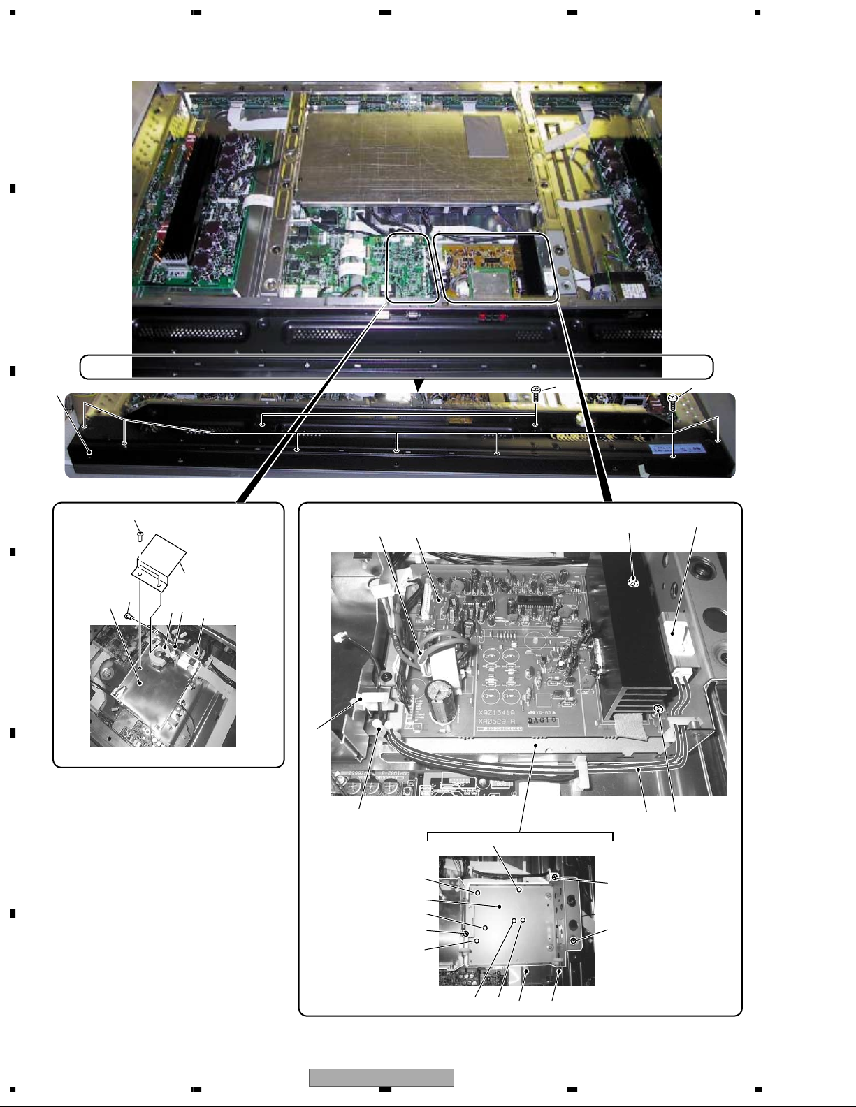
2.8 MIDDLE LAYER SECTION (2)
A
B
19
C
7
17
1
6
3
12
D
4
2
5
5
11
13
18
15
E
F
20
1234
16
PDP-503PC
10
10
11
8
11
9
8
11
10
8
5
5
14
13
Page 21

5678
MIDDLE LAYER SECTION (2) parts List
Mark No. Description Part No.
1 AUDIO AMP Assy AWZ6687
2 Toroidal Core (L2) ATX1042
3 Screw ABA1294
4 Edge Saddle AEC1571
5 Wire Saddle AEC1745
6 IF Sheet AMR3298
7 Nyron Rivet AEP-211
8 PCB Spacer AEC1570
9 Audio Base ANA1687
10 Spacer AEC1360
A
11 Screw AMZ30P060FZK
12 IF Shield ANA1675
13 Screw PMB30P060FNI
14 J215 3P Housing Wire ADX2757
15 Power Switch (S2) ASG1089
16 Niplocker BEC1136
17 J214 3P Housing Wire ADX2735
18 Screw TBZ40P080FZK
19 Terminal Panel P ANG2537
B
C
D
56
PDP-503PC
E
F
7
8
21
Page 22

1234
2.9 UPPER LAYER SECTION (1)
A
B
2
7
C
J201
J202
D
813
112
J5002
9
6
10
5
15
2
16
14
Caution in the MR INTERFACE Assy Replacement
Set the slide switches in accordance with applicable
model when replacing the MR INTERFACE Assy.
E
PDP-503P → →
PDP-503PE ← →
PDP-503PU → →
S4001
CBIT_1
S4004
CBIT_0
S4001
(CBIT_1)
Note 1 : When there is not S4004, set only S4001.
Note 2 : When there are not S4001 and S4004, setting
F
22
is unnecessary.
PDP-503PC
1234
S4004
(CBIT_0)
Page 23

5678
UPPER LAYER SECTION (1) parts List
Mark No. Description Part No.
1 MR INTERFACE Assy AWZ6699
2 Screw AMZ30P060FZK
3• • • • •
4• • • • •
5 Screw PMZ26P080FZK
6 Hexagonal Head Screw BBA1051
7 J201 Flexible Flat Cable ADD1194
8 J202 Flexible Flat Cable ADD1194
9 J104 3P Housing Wire ADX2732
10 J214 3P Housing Wire ADX2735
A
11 • • • • •
12 J118 Wire P ADX2765
13 J113 Wire PJ ADX2718
14 Toroidal Core (L3) ATX1042
15 Screw ABA1294
16 J111 14P Housing Wire ADX2730
B
C
D
56
PDP-503PC
E
F
7
8
23
Page 24
1234
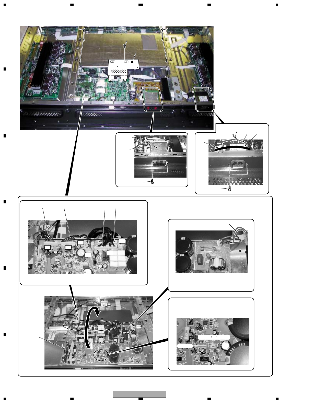
2.10 UPPER LAYER SECTION (2)
1313
A
B
C
1315
1314
1
J5003
1313
18
12
4
6
3
5
10
89
D
P1
E
P6
P2
P5
11
12
P4
P3
2
SW101
F
24
1234
PDP-503PC
200V 100V
Page 25

5678
UPPER LAYER SECTION (2) parts List
Mark No. Description Part No.
1 SP TERMINAL Assy AWZ6688
2 SW Power Supply Module AXY1059
3 Screw BPZ30P080FZK
4 AC Inlet with Noise Filter (CN1) AKP1223
5 Screw BMZ30P060FZK
6 Ferrite Core (L1) ATX1032
7 • • • • •
8 J118 Wire P ADX2765
9 J101 13P Housing Wire ADX2726
10 J103 13P Housing Wire ADX2700
>
>
>
A
11 J102 Wire E ADX2782
12 J105 Wire PB ADX2722
13 Screw AMZ30P060FZK
14 IF Earth Metal ANA1690
15 Screw PMB30P060FNI
16 • • • • •
17 • • • • •
18 J114 Earth Wire ADX2709
B
C
D
56
PDP-503PC
E
F
7
8
25
Page 26

1234
2.11 FRONT CASE SECTION
10
2
22
21
17
6
7
3
16
10
8
16
12
25
10
Foil Side
1
20
A
B
C
24
23
16
16
10
D
13
FRONT CASE SECTION parts List
Mark No. Description Part No.
1 FRONT KEY Assy AWZ6656
E
2 Front Case 50 (P) AMB2722
3 Rivet AEC1877
4• • • • •
5• • • • •
6 Ferrite Core (L5) ATX1043
7 Lead Cover (P) AMR3341
8 Pioneer Badge AAM1091
9• • • • •
NSP 10 Panel Holder ANG2508
11 Front Spacer AEC1896
F
12 • • • • •
13 Panel Cushion V AED1199
14 Panel Cushion H AED1198
11
16
14
11
14
10
10
16
15
11
11
13
Mark No. Description Part No.
15 Protect Panel Assy AMR3304
16 Screw ABZ30P050FZK
17 Screw VMZ30P060FZK
18 • • • • •
19 • • • • •
20 PCB Spacer AEC1913
21 J213 Flexible Flat Cable ADD1193
NSP 22 Flexible Seal (P) AEH1052
23 Power Button AAD4113
24 Coil Spring ABH1108
25 Serial Sheet AAX2609
26
1234
PDP-503PC
Page 27

5678
1
1
2
5
67
4
3 3
10
3 3
4
4
4
4
3
3 38 93
Bottom View
3 3
4
4
4
4
2.12 REAR SECTION
A
B
REAR SECTION parts List
Mark No. Description Part No.
1 Rear Case (50P) ANE1609
2 Gascket L50 ANK1701
3 Screw AMZ30P060FZK
4 Screw TBZ40P080FZK
5 Cleaning Label AAX2941
NSP 6 Name Label (C) AAL2435
7 Bolt Caution Label AAX2942
8 Terminal Display Label P AAX2929
9 Terminal Display Label L AAX2930
10 Label (Blue 8) AAX2786
C
D
E
PDP-503PC
56
F
7
8
27
Page 28

1234
2.13 PDP SERVICE ASSY 503 (AWU1068)
PDP Service Assy (AWU1068) consists of the following parts.
Mark No. Description Part No.
A
NSP Panel Chassis (50) Assy AWU1066
NSP Front Chassis V ANA1661
NSP Front Chassis H (W) ANA1679
NSP Front Chassis H ANA1683
NSP Sub Frame L ANG2499
Mark No. Description Part No.
Insullation Sheet AMR3263
Scan Insullation Sheet AMR3271
Niplocker BEC1136
Card Corner Holder BEC1144
Screw ABA1283
NSP Sub Frame R ANG2500
Scan IC Spring (L) ABK1026
Scan IC Spring (R) ABK1027
NSP Metal Fitting ANG2464
FPC Cushion 50 AEB1370
B
NSP PCB Spacer AEC1121
Locking Card Spacer AEC1736
Circuit Board Spacer AEC1872
Circuit Board Spacer AEC1873
Spacer AEC1896
NSP Card Spacer AEC1902
Wire Saddle AEC1904
Panel Cushion H AED1198
Panel Cushion V AED1199
C
V Cushion AED1205
Screw ABA1294
Screw ABZ30P060FMC
Screw BMZ30P060FMC
Screw PMB30P060FNI
Screw VBB30P100FNI
Bolt ABA1259
Corner Pad AHA2203
Corner Pad AHA2204
Upper Carton AHD3119
Under Carton AHD3120
Packing Sheet AHG1291
Fitting Board AHK1012
Washer WB80FZB
V Cushion AED1205
2.14 PANEL CHASSIS (50) ASSY (AWU1066)
Panel Chassis (50) Assy (AWU1066) consists of the following parts.
• Parts List • List of Assy
Mark Description Part No.
NSP SCAN FUKUGO ASSY AWV1968 *
NSP ADDRESS FUKUGO ASSY AWV1900 *
NSP Address Module (IC1 - IC40) AXF1110
NSP FPC (0003) ADY1065
D
NSP FPC (J0001) ADY1066
NSP 1..Chassis Assy ANA1711
NSP 2..Chassis ANA1655
NSP 2..Base Chassis ANA1656
NSP 2..Scan Heatsink ANH1609
NSP 2..Corner Angle A ANG2457
NSP 2..Corner Angle B ANG2458
2..Panel Silicone Sheet AEH1055
NSP 2..Tube Cover AMR3262
E
2..Silicone Sheet 50 AEH1037
2..Adhesive Tape 50 AEH1038
2..Adhesive Tape B (50) AEH1051
2..Seet A AEC1923
2..Seet B AEC1924
2..Rear Coner Label AEH1051
Mark
NSP 1..SCAN FUKUGO ASSY AWV1968
2..SCAN (A) ASSY AWZ6722
2..SCAN (B) ASSY AWZ6723
2..X CONNECTOR (A) ASSY AWZ6732
2..X CONNECTOR (B) ASSY AWZ6733
2..BRIDGE A ASSY AWZ6734
2..BRIDGE B ASSY AWZ6735
2..BRIDGE C ASSY AWZ6736
2..BRIDGE D ASSY AWZ6737
2..CLAMP A ASSY AWZ6738
2..CLAMP B ASSY AWZ6739
2..CLAMP C ASSY AWZ6740
2..CLAMP D ASSY AWZ6741
NSP 1..ADDRESS FUKUGO ASSY AWV1900
NSP 2..ADR CONNECT A ASSY AWZ6626
NSP 2..ADR CONNECT B ASSY AWZ6627
NSP 2..ADR CONNECT C ASSY AWZ6628
NSP 2..ADR CONNECT D ASSY AWZ6629
2..ADR RESONANCE ASSY AWZ6750
Description Part No.
Pin Grommet AEC1015
Card Spacer AEC1889
Scan Silicone Sheet AEH1057
NSP Plasma Panel Assy AAV1238
F
Screw VBB30P100FNI
28
1234
PDP-503PC
Page 29
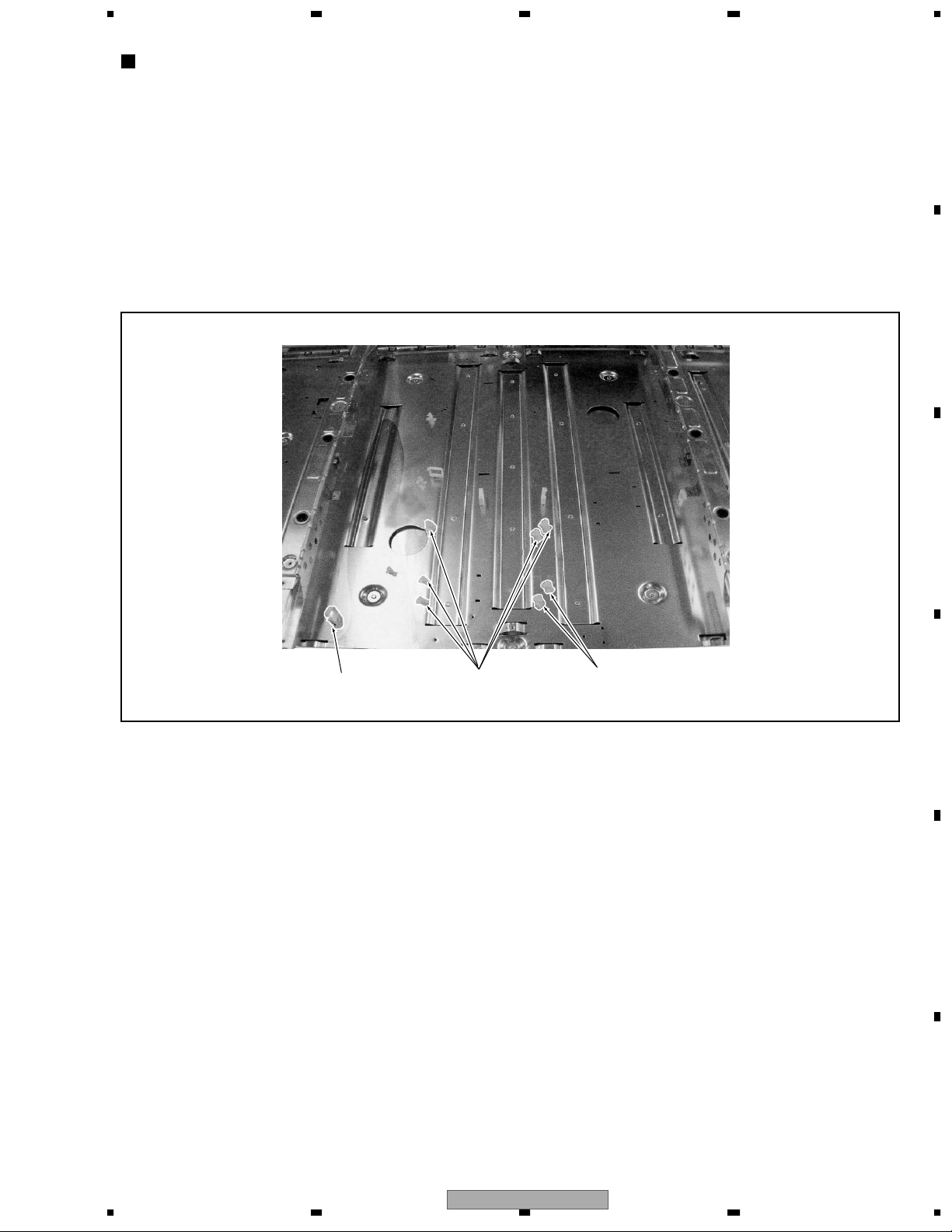
PDP Service Assy 503 (AWU1068)
Circuit Board Spacer
(AEC1872)
Circuit Board Spacer
(AEC1872)
Caution in Replacement of Chassis Block
Please order the PDP Service Assy 503 (AWU1040) when replacing the Chassis block.
PDP Service Assy 503 is all common use parts of for business, public use and module.
Supply it by the state that installed Circuit Board Spacer (AEC1872) and Wire Saddle (AEC1904) as follows.
Therefore need to remove it in accordance with model.
Confirm character carved a seal near the parts, and remove it.
P : Public exclusive use
W : Module exclusive use
PW : Common use of public use and module
∗ In case of this unit, the parts that "W" is marked removes all.
Wire Saddle
(AEC1904)
(There is marking of "P" nearby.)
5678
A
B
C
D
E
56
PDP-503PC
F
7
8
29
Page 30
1234
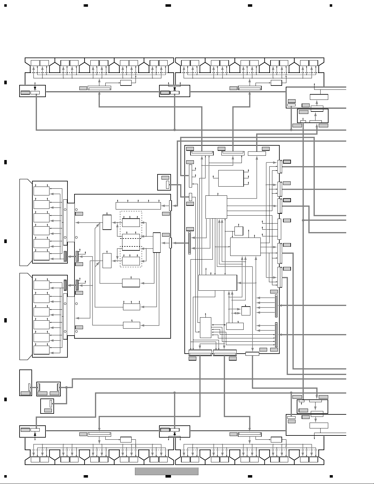
3. BLOCK DIAGRAM AND SCHEMATIC DIAGRAM
3.1 BLOCK DIAGRAM
3.1.1 OVERALL DIAGRAM
A
B
C
D
E
DriverICDriver
VADR2
CLA1
CLAMP A
ASSY
SCAN (A) ASSY
(UPPER)
SCAN (B) ASSY
(LOWER)
FRONT KEY
ASSY
IC
ADR CONNECT A
ASSY
CLAMP
IC5
VCC_VH
IC6201
ADD
PSUS
SEL_PULSE
IC5
VCC_VH
IC6202
ADD
SEL_PULSE
IC5
VCC_VH
IC6203
ADD
SEL_PULSE
IC5
VCC_VH
IC6204
ADD
SEL_PULSE
IC5
VCC_VH
IC6205
ADD
SEL_PULSE
IC5
VCC_VH
IC6206
ADD
SEL_PULSE
SEL_PULSE
SEL_PULSE
SEL_PULSE
SEL_PULSE
SEL_PULSE
SEL_PULSE
FRONT KEY CONN
ASSY
IC5
IC6001
ADD
IC5
IC6002
ADD
IC5
IC6003
ADD
IC5
IC6004
ADD
IC5
IC6005
ADD
IC5
IC6006
ADD
VCC_VH
SCAN
VCC_VH
VCC_VH
VCC_VH
VCC_VH
VCC_VH
SCAN
PSUS
DriverICDriver
IC
DriverICDriver
AA1
Y DRIVE ASSY
Y4
PSUS
VCC_VH
V_IC5V
Y3
VCC_VH
V_IC5V
Y5
PSUS
Y6
IC
DriverICDriver
IC
CLK/LE
IC6501
Buffer IC
VC_VF+ VC_VF- V_OFS VCC_VH V_IC5V
DC/DC Conv.
VCP
Y-SUS
MASK
Block
VCP
Y-SUS
MASK
Block
Scan Signal
VC_VF+
Block
+5V +15V
VSUS
IC2206
Pulse Module
+15V VSUS
+Reset Block
+5V +15V VSUS
IC2204
Pulse Module
+15V
Soft-D
Block
VC_VF- V_OFS
Offset
Block
V_IC5V
Photo Coupler
Block
DriverICDriver
THERMAL
SENSOR
ASSY
Drive
Signal
Drive
Signal
IC
VADR2
BGA1
BRIDGE A
ASSY
TE1
Y1
Y2
Logic
Block
VADR2
CLAMP
DriverICDriver
IC
DriverICDriver
IC
ADR CONNECT B
ASSY
AB1
D8 D9 D16
D1
+12V
V+5V_STB
+12V
DC/DC Conv.
V+3V
IC1703
XY Drive
Gen.
Sub-Field Conv.
TXD/RX
Module
DIGITAL VIDEO
ASSY
KL_U0:2
XDRV_SIG
ADL_LE_UL
ADL_LE_DL
V+3V
X180
Clock
Gen.
IC1301 (IC31 L)
Sub-Field Conv.
for Left with Field Memory
V+3V
IC1101
Panel UCOM
+12V
D18
D6
Sequence Pattern
YDRV_SIG
SCAN_SIG
V+3V_I
V+2V_I
IC1401 (IC31 R)
for Right with Field Memory
ADCLK_DR
V+5V_STB
IC120
Module
UCOM
D13D12
DriverICDriver
IC
ADR RESONANCE
ASSY
V+5V
V+3V
V+2V
V+3V_IC
V+2V_IC
V+3V
IC119
Flash
ROM
DriverICDriver
IC
CLK/LE
IC6601
Buffer IC
SUB ADDRESS A
ASSY
D10
D11
V+2V
V+3V
V+5V_STB
D15
D14
D2
BA2:9
BB2:9
GA2:9
GB2:9
RA2:9
RB2:9
TXD0/RX0
RE
LED_SIG
I2
D3D17
DriverICDriver
K2
K1
SAA3
+60
SAA1 SAA2
D7
D4
IC
VADR2
Q6706 - Q6711
VADR Gen.
ADR_CO
F
30
SW21 KL21 KL22
IR (P)
ASSY
RE1
CLAMP C
ASSY
CLC1
CLAMP
VADR2
Driver
Driver
IC
IC
1234
ADR CONNECT D
ASSY
DriverICDriver
IC
AD1
DriverICDriver
SUB ADDRESS B
ASSY
ADR RESONANCE
DriverICDriver
ASSY
IC
CLK/LE
IC6801
Buffer IC
DriverICDriver
BRIDGE C
ASSY
BGC1
IC
VADR2
CLAMP
VADR2
IC6901
Buffer IC
CLK/LE
IC
DriverICDriver
IC
DriverICDriver
DriverICDriver
ADR CONNECT C
ASSY
IC
DriverICDriver
AC1
IC
SAB1 SAB2
+60
SAB3
K2
IC
DriverICDriver
K1
ADR_CO
Q6706 - Q6711
VADR Gen.
VADR2
IC
PDP-503PC
Page 31
5678
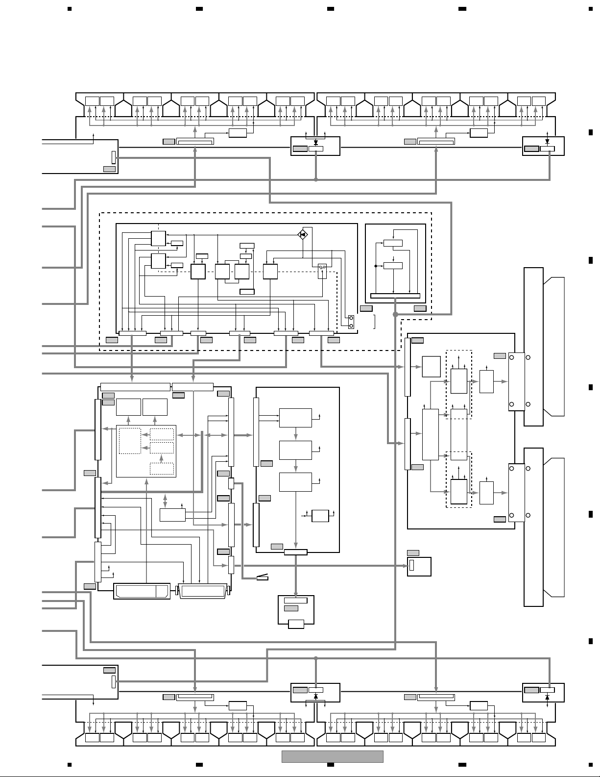
Note : When ordering service parts, be sure to refer to "EXPLODED VIEWS and PARTS LIST" or "PCB PARTS LIST".
DriverICDriver
DriverICDriver
IC
IC
DriverICDriver
IC
DriverICDriver
IC
DriverICDriver
IC
DriverICDriver
IC
DriverICDriver
IC
DriverICDriver
DriverICDriver
IC
IC
DriverICDriver
A
IC
CLK/LE
VADR2
ADR CONNECT C
ASSY
AC1
IC6801
Buffer IC
K3
SW POWER SUPPLY MODULE
SW POWER SUPPLY Block
+13.5V
-9V
T101
Switching
+13.5V
+6.5V
+15V
+12V
STB5V
-9V
+6.5V
T102
+12V
Q115
Switching
Q117
STB5V
Switching
Q119
VADR
Switching
VSUS_CONT
+15V
M111
Q112
T105T104T103
M114
STB5V
T105
LIVE
NEUTRAL
SECONDARY
+13.5V
P1 P2 P5 P6 P3 P4
AUDIO AMP ASSY
R23
L
R
FOCUS
SRS
R27
R24
R11
AUDIO_SIG (L/R)
A24
A21
TRAP SW
L
R
Volume & Tone
A22
R3
R22
R21
KEY1
KEY2
R2
IC4203
EEPROM
(HDCP KEY)
• Scalling
• Gamma
TMDS Receiver
V+5V_ST
V+5V_ST
IC4204
(Sil861)
IC4201
EEPROM
(EDID)
I2C
Interface
Copy Guard
Release
TMDS
Receiver
I2C_BUS (SCL/SDA)
IC4011
I/O Expander
LED_SIG
TXD/RXD
SR_UP
SR_DW
TMDS with HDCP
R26
MR INTERFACE
ASSY
V+5V_DIG
System Cable Connector
VADR2
BGB1
BRIDGE B
ASSY
RC101
PRIMARY
POWER (RELAY)
VSUS
-9V
IC5202
& Balance
L, R
IC5201
SRS & Focus
L, R
IC5002
Power Amp.
L, R
L, R
SP21
SP OUT
VADR2
CLAMP
RL101
+15V
VSUS
+12V
+12V
+15V
+12V+13.5V
IC5001
Reg.
SP TERMINAL
ASSY
ADR CONNECT D
ASSY
V MID CLAMP Block
CLAMP
CLAMP
P7 VM1
LIVE
AC IN
NEUTRAL
AD1
X DRIVE ASSY
X1
DC/DC
Conv.
Block
Drive
Signal
+5V
Logic
Block
X2
Drive
Signal
L1
LED
ASSY
VSUS
CLK/LE
+5V
IC3200
Pulse
Module
+Reset
Pulse
Block
+5V
IC3201
Pulse
Module
+15V
+15VV_RN
+15VVSUS
IC6901
Buffer IC
VCP
X_SUS
MASK
VCP
X_SUS
MASK
X3
P_SUS
P_SUS
X4
VADR2
CLAMP
CLB1
CLAMP B
ASSY
X CONNECTOR (A) ASSYX CONNECTOR (B) ASSY
B
C
D
E
VADR2
DriverICDriver
K3
ADR CONNECT B
ASSY
IC
DriverICDriver
AB1
IC
DriverICDriver
IC
CLK/LE
IC6601
Buffer IC
DriverICDriver
IC
BRIDGE D
ASSY
BGD1
DriverICDriver
IC
VADR2
CLAMP
VADR2
PDP-503PC
56
DriverICDriver
IC
ADR CONNECT A
ASSY
DriverICDriver
IC
7
AA1
DriverICDriver
CLAMP D
ASSY
CLD1
IC
VADR2
CLAMP
F
IC6501
Buffer IC
CLK/LE
DriverICDriver
IC
IC
DriverICDriver
31
8
Page 32

1234
3.1.2 MR INTERFACE ASSY
A
B
C
CN4003 (DVI)
TMDS
6
DDC_SCL
7
DDC_SDA
14
DDC5V
CN4002 (MDR)
15
SR_UP
11
M_TXD
1
M_RXD
IC4204
TMDS_RXCORE CONTENT_PROTECTION
IC4201
(DDC_ROM)
Q4014 (REM_CUT)
Q4018 (INV)
C4043
(HPF)
IC4006 (REM_SLICER)
Q4008 (2.5V_REG)
IC4006 (TTL → CMOS CONVERT)
IC4006 (BUFF)
Q4201, Q4202
(5V ↔ 3.3V
I2C_LEVEL_SHIFT)
IC4010
(NON_SYSTEM_DET)
SCALING
IC4011
(I/O_EXPANDER)
IC4005
(I/O_EXPANDER)
S4001, S4004, etc
(MODEL_INFO)
IC4012 (IC2_SW)
IC4013
(STB_DET)
IC4203
(CONF_ROM)
Q4001, Q4002 (I2C_SW)
V+5V_DIG
Q4005, Q4006
(5V ↔ 3.3V
I2C_LEVEL_SHIFT)
8bit_DIGITAL
× RGB
DDC_SCL
DDC_SDA
PMST
A_SCL
A_SDA
RXD0
TXD0
CN4004, CN4005
14
SR_DOWN
D
5
SM_POW
R4093
7
8
CCKM
CSEN2
R4098
(BIAS)
E
2010
SPL
13
4
SPR
Q4012 (INV) REM
Q4007 (BUFF)
IC4010 (BUFF)
IC4007 (COMPR)
+
IC4008, IC4009 (REM_SW)
Q4011 (DRIVER)
Q4401 (BUFF)
Q4402 (BUFF)
SM_POW
CCKM
SW_TRG
F_KEY1
F_KEY2
LED_G
LED_R
I2C
L_CH
R_CH
CN4401
LED_G
CN4007
REM
KEY1
KEY2
LED_R
CN4009
F
32
PDP-503PC
1234
Page 33

5678
No. Name Description Voltage at INPUT4 NTSC Input
1
2
3
4
5
6
7
8
9
10
11
12
13
14
15
16
17
18
19
20
M_RXD
GND
SENCE
SPR
SMPOW
GND
CCKM
CSEN2
CSEN1
SPL
M_TXD
GND
SPR
SR_DW
SR_UP
GND
FRASH_W
SRST
GND
SPL
232C bus (PDP → MR)
Connecting detection for MR
Audio signal R ch
MR relay control
System activation detection
System activation signal
Not used
Audio signal L ch
232C bus (MR → PDP)
Audio signal R ch
Remote control signal
MDR connecting detection signal
multiplex remote control signal
Not used
Not used
Audio signal L ch
0-5V swing square wave
0.0V DC
Analog audio signal wave
3.5V DC
1.9V DC
5.0V DC
Analog audio signal wave
0-3.3V swing square wave
Analog audio signal wave
5.0V DC
3.75V DC
Analog audio signal wave
No. Name Description Voltage at INPUT4 NTSC Input
1
2
3
4
5
6
7
8
9
10
11
12
13
14
15
16
17
18
19
20
21
22
23
24
RX2RX2+
GND
NC
NC
DDC_SCL
DDC_SDA
NC
RX1RX1+
GND
NC
NC
DDC_+5V
GND
HPD
RX0RX0+
GND
NC
NC
GND
RXC+
RXC-
DVI signal
DVI signal
I2C for DDC
I2C for DDC
DVI signal
DVI signal
I2C power supply for DDC
HOT_PLUG detection
DVI signal
DVI signal
DVI signal
DVI signal
DVI signal
DVI signal
0-5V swing square wave
0-5V swing square wave
DVI signal
DVI signal
5.0V DC
5.0V DC
DVI signal
DVI signal
DVI signal
DVI signal
CN4002 (MDR Connector) (↔ Media Receiver)
CN4004 (50P_FFC Connector) (↔ DIGITAL VIDEO Assy) CN4005 (50P_FFC Connector) (↔ DIGITAL VIDEO Assy)
CN4003 (DVI Connector) (↔ Media Receiver)
No. Name Description Voltage at INPUT4 NTSC Input
1
2
3
4
5
6
7
8
9
10
11
12
13
14
15
16
17
18
19
20
21
22
23
24
25
26
27
28
29
30
31
32
33
34
35
36
37
38
39
40
41
42
43
44
45
46
47
48
49
50
GND
GND
NC
NC
NC
NC
BB0
BA0
BB1
BA1
BB2
BA2
BB3
BA3
BB4
BA4
BB5
BA5
BB6
BA6
BB7
BA7
GND
GND
NC
NC
NC
NC
GB0
GA0
GB1
GA1
GB2
GA2
GB3
GA3
GB4
GA4
GB5
GA5
GB6
GA6
GB7
GA7
GND
GND
NC
NC
GND
GND
8 bit video signal
8 bit video signal
8 bit video signal
8 bit video signal
8 bit video signal
8 bit video signal
8 bit video signal
8 bit video signal
8 bit video signal
8 bit video signal
8 bit video signal
8 bit video signal
8 bit video signal
8 bit video signal
8 bit video signal
8 bit video signal
8 bit video signal
8 bit video signal
8 bit video signal
8 bit video signal
8 bit video signal
8 bit video signal
8 bit video signal
8 bit video signal
8 bit video signal
8 bit video signal
8 bit video signal
8 bit video signal
8 bit video signal
8 bit video signal
8 bit video signal
8 bit video signal
0-3.3V swing square wave
0-3.3V swing square wave
0-3.3V swing square wave
0-3.3V swing square wave
0-3.3V swing square wave
0-3.3V swing square wave
0-3.3V swing square wave
0-3.3V swing square wave
0-3.3V swing square wave
0-3.3V swing square wave
0-3.3V swing square wave
0-3.3V swing square wave
0-3.3V swing square wave
0-3.3V swing square wave
0-3.3V swing square wave
0-3.3V swing square wave
0-3.3V swing square wave
0-3.3V swing square wave
0-3.3V swing square wave
0-3.3V swing square wave
0-3.3V swing square wave
0-3.3V swing square wave
0-3.3V swing square wave
0-3.3V swing square wave
0-3.3V swing square wave
0-3.3V swing square wave
0-3.3V swing square wave
0-3.3V swing square wave
0-3.3V swing square wave
0-3.3V swing square wave
0-3.3V swing square wave
0-3.3V swing square wave
No. Name Description Voltage at INPUT4 NTSC Input
1
2
3
4
5
6
7
8
9
10
11
12
13
14
15
16
17
18
19
20
21
22
23
24
25
26
27
28
29
30
31
32
33
34
35
36
37
38
39
40
41
42
43
44
45
46
47
48
49
50
NC
NC
NC
NC
RB0
RA0
RB1
RA1
RB2
RA2
RB3
RA3
RB4
RA4
RB5
RA5
RB6
RA6
RB7
RA7
GND
CLK
GND
DE
GND
HD
GND
VD
GND
A_SCL
F_KEY1
PMST
SMPOW
A_MUTE
CCKM
M_STATE
SW_STC
A_NG
SW_TRG
F_KEY2
A_SDA
*LED_G
TXD0
*LED_R
RXD0
DDC_SCL
REM
DDC_SDA
GND
GND
8 bit video signal
8 bit video signal
8 bit video signal
8 bit video signal
8 bit video signal
8 bit video signal
8 bit video signal
8 bit video signal
8 bit video signal
8 bit video signal
8 bit video signal
8 bit video signal
8 bit video signal
8 bit video signal
8 bit video signal
8 bit video signal
Clock
Data enable
Horizontal sync. signal
Vertical sync. signal
I2C bus
Front key signal 1
MDR connecttion Detect signal
MR relay control
Audio mute
System activation detect
SiI861 I2C bus master infomation
Not used
Not used
System activation signal
Front key signal 2
I2C bus
Green LED control signal
232C bus
Red LED control signal
232C bus
I2C for DDC
Remote control signal
I2C for DDC
0-3.3V swing square wave
0-3.3V swing square wave
0-3.3V swing square wave
0-3.3V swing square wave
0-3.3V swing square wave
0-3.3V swing square wave
0-3.3V swing square wave
0-3.3V swing square wave
0-3.3V swing square wave
0-3.3V swing square wave
0-3.3V swing square wave
0-3.3V swing square wave
0-3.3V swing square wave
0-3.3V swing square wave
0-3.3V swing square wave
0-3.3V swing square wave
0-3.3V swing square wave (40MHz)
0-3.3V swing square wave (+ polarity)
0-3.3V swing square wave
(- polarity 48.4kHz)
0-3.3V swing square wave
(- polarity 60.0Hz)
0-5V swing square wave
5.0V DC
3.75V DC
5.0V DC
0.0V DC
1.9V DC
0.0V DC
5.0V DC
5.0V DC
0-5V swing square wave
0.0V DC
0-5V swing square wave
5.0V DC
0-5V swing square wave
0-5V swing square wave
5.0V DC
0-5V swing square wave
Voltages
A
B
C
D
E
F
56
PDP-503PC
7
8
33
Page 34

1234
3.1.3 DIGITAL VIDEO ASSY
A
MR INTERFACE
B
C
IC4005
Expander
IC4011
Expander
AUDIO
ASSY
IC4204
SiI861
To
MR
To
Assy
RGB 2 phase 8 bit
VD
HD
DE
CLK
RXDO
TXDO
A_SCL, A_SDA
DIGITAL VIDEO ASSY
Reflesh-rate
Det.
AND
CN1201
EXT_RXD
EXT_TXD
RXDO
TXDO
WE_PN
3.3V
Line
Buffer
HD
VD
RESET
EXD RXD
EXD TXD
RESET
Address BUS
Data BUS
Control Signal
3.3V
IC1191
Flash ROM
3.3V
Reset IC
3.3V
2.5V
IC1301 (IC31 L)
IC1401 (IC31 R)
APLR
VD 31
IC1101
(HD64F2328VF)
Panel Microcomputer
3.3V → 5.0V5.0V → 3.3VReset IC
RST PU
(M30624FGAFP)
Module Microcomputer
PD_TRIGGER
TEMP1
RST2
IC1207
AC_OFF
(PD6358)
DRAM
(PD6358)
DRAM
3.3V
RXD
BUSY
REQ_PU
IC1703 (IC23)
(PE5064)
Address
Resonance
STOPB
Control
PC_VIDEO
ADR_K_EMG
AND
APD MUTE
STB5V
RELAY
5V
IIC BUS
Address Data
Address Data
OR
ADR PD
OR
Sustain
Control
ADR K PD U
ADR K PD D
STB5V
EEP
ROM
DCC_PD
5V
RESONANCE
Panel W/B ADJ.
Hour/Pulse meter
DEW DET
5V
Converter
ADR CONNECT A - D
Assy (Left section)
ADR CONNECT A - D
Assy (Right section)
Y DRIVE Assy
X DRIVE Assy
ADR
Assy
pn
3.3V
2.5V
DC/DC
Block
STB5V
D
THERMAL
SENSOR
Assy
DIG. ADR. PD
SW POWER SUPPLY Module
12V
STB5V
E
F
34
1234
PDP-503PC
Page 35

5678
23
21
579
1113151719
PN_MUTE
XNR-U
XSUS-B
XSUS-U
XSUS-D
XSUS-G
XSUS-MSK
XCP-MSK
XNR-D1
XNR-D2
CN3001
X2
12348
11
CN3101
X1
XNR_U
XNR_U
24536
65234
9
IC3004
TC74ACT540FT
IC3008
TC74ACT541FT
18
17
14
1415181716
16
15
152346897
10
IC3008
PE1012A
202322211917161815
2345786
9
IC3001
TC74ACT541FT
IC3102
HCPL-M611
IC3101
TC74ACT541FT
IC3200
STK795-460
Pulse Module
IC3201
STK795-460
Pulse Module
T3701
VRN D-D CONV.
XCP-MSK
XSUS-MSK
VCP
PLD
SUSOUT A
37-40
29,30
K3105
PSUS
K3107
IC3103,IC3104
TND301S
Q3103,
Q3107
Q3104,
Q3109
Q3105,
Q3124
Q3106,
Q3125
SUSOUT B
37-40
29,30
K3106
IC3106,IC3107
TND301S
Q3110,
Q3114
Q3111,
Q3115
Q3112,
Q3126
Q3113,
Q3127
To
X CONNECTOR
ASSY
IC3110
TND301S
IC3113
TND301S
charge pump
circuit
From DIGITAL VIDEO ASSY
Photo
coupler
2-9 11-18
+15V
DGND
XDRIVE_PD
XDC_DC_PD
VSUS
SUSGND
SUSGND
SUSGND
P.D.
DET.
18171615131214
11
14
16
18
20
14
16
18
20
VSUS 225V
VRN UVP
VRN OVP
Q3116
Q3120
Q3122
Q3128
XNR-D1
XNR-D2
VRN-300V
XDRIVE_PD
3.1.4 X DRIVE ASSY
A
B
C
D
PDP-503PC
56
7
E
F
35
8
Page 36

1234
3.1.5 Y DRIVE ASSY
A
CLR
27
CLK
25
OC1
30
OC2-1
31
40
LE
42
AB
43
SI1
45
SI2
IC2001
B
TC74ACT541FT
OC2-2
Photo Coupler
Photo Coupler
Photo Coupler
Photo Coupler
Photo Coupler
Photo Coupler
Photo Coupler
Photo Coupler
IC2501,IC2502,
IC2505,IC2510,
IC2512,IC2513,
IC2514,IC2525,
HCPL-M611
TC74ACT540FT
Photo Coupler
IC2516
HCPL-M611
C
SUS muteDET.
circuit
IC2005
33
24
19
21
9
10
12
18
13
16
15
22
46
Y2
TC74ACT541FT
IC2007
TC74ACT540FT
Q2102
IC2006
PE1013
Dew DET.
OC2-2
PN_MUTE
YPR-U1
YPR-U2
YSUS-B
YSUS-U
YSUS-D
YOFS
D
YSUS-G
YCP-MSK
YSUS-MSK
YSOFT-D
DEW_DET
IC2504
TC74ACT540FT
IC2506
IC2004
TC74ACT541FT
TC74ACT540FT
+13.5V
-9V
YPR-U1
circuit
IC2005
TC74ACT541FT
Vsus
IC5V
E
1
+15V
-9V
VSUS
VSUS
2
3
4
5
6
7
10
11
13
14
SUSGND
D. GND
D. GND
+13.5V
YDRIVE_PD
YDC_DC_PD
VOFS_ADJ
SUSGND
SUSGND
F
P.D.
DET.
IC5V UVP
VOFS UVP
VOFS OVP
VH UVP
VH OVP
IC5V, VF
D-D CONV.
VOFS D-D
CONV.
VH D-D CONV.
VH
IC2503
YCP-MSK
YPR-U2
YSUS-MSK
YSOFT-D
YOFS
IC5V
VF+
VF-
VOFS
VH
Y5
VH
Pulse Module
14
(STK795-460)
16
18
20
Pulse Module
14
(STK795-460)
16
18
20
charge pump
To SCAN ASSY
(Lower)
CN2501CN2502
To SCAN ASSY
(Upper)
Y3
IC2206
IC2214
circuit
Photo Coupler
IC2202
HCPL-M611
Photo Coupler
IC2208
HCPL-M611
36
1234
PDP-503PC
Page 37
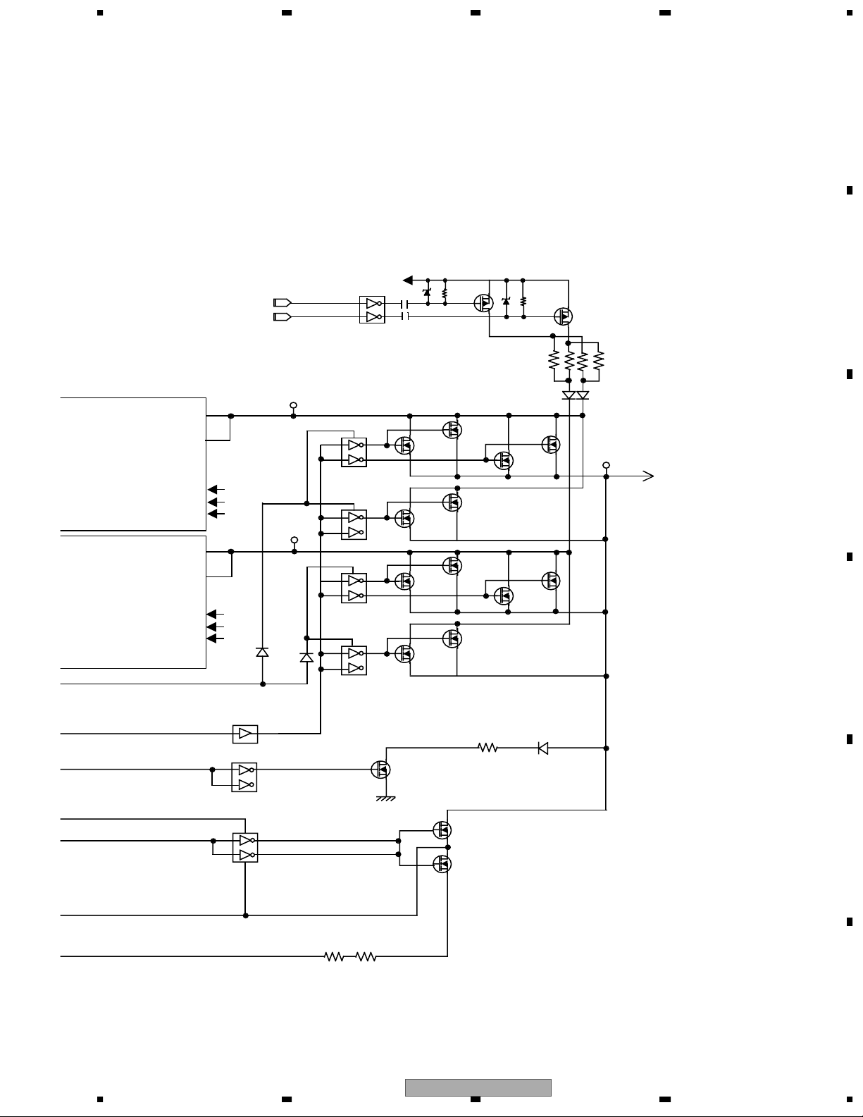
5678
A
YPR-U1
YPR-U2
SUSOUT A
37-40
29,30
5V
15V
Vsus
SUSOUT B
37-40
29,30
5V
15V
Vsus
VSUS
IC2203
TND301S
K2203
K2212
VCP
IC2212
TND301S
Q2218
IC2213
TND301S
Q2220
IC2216
TND301S
Q2226
IC2217
TND301S
Q2232
Q2204
Q2219
Q2221
Q2217
Q2233
Q2215
Q2228
Q2227
Q2216
Q2205
K2220
PSUS
TO
Y CONNECTOR
ASS'Y
B
C
D
IC2201
TC74ACT541FT
2-9
11-18
IC2204
TND301S
IC2210
TND301S
Q2210
SUSGND
Q2211
Q2212
PDP-503PC
56
PSUS
E
F
7
8
37
Page 38
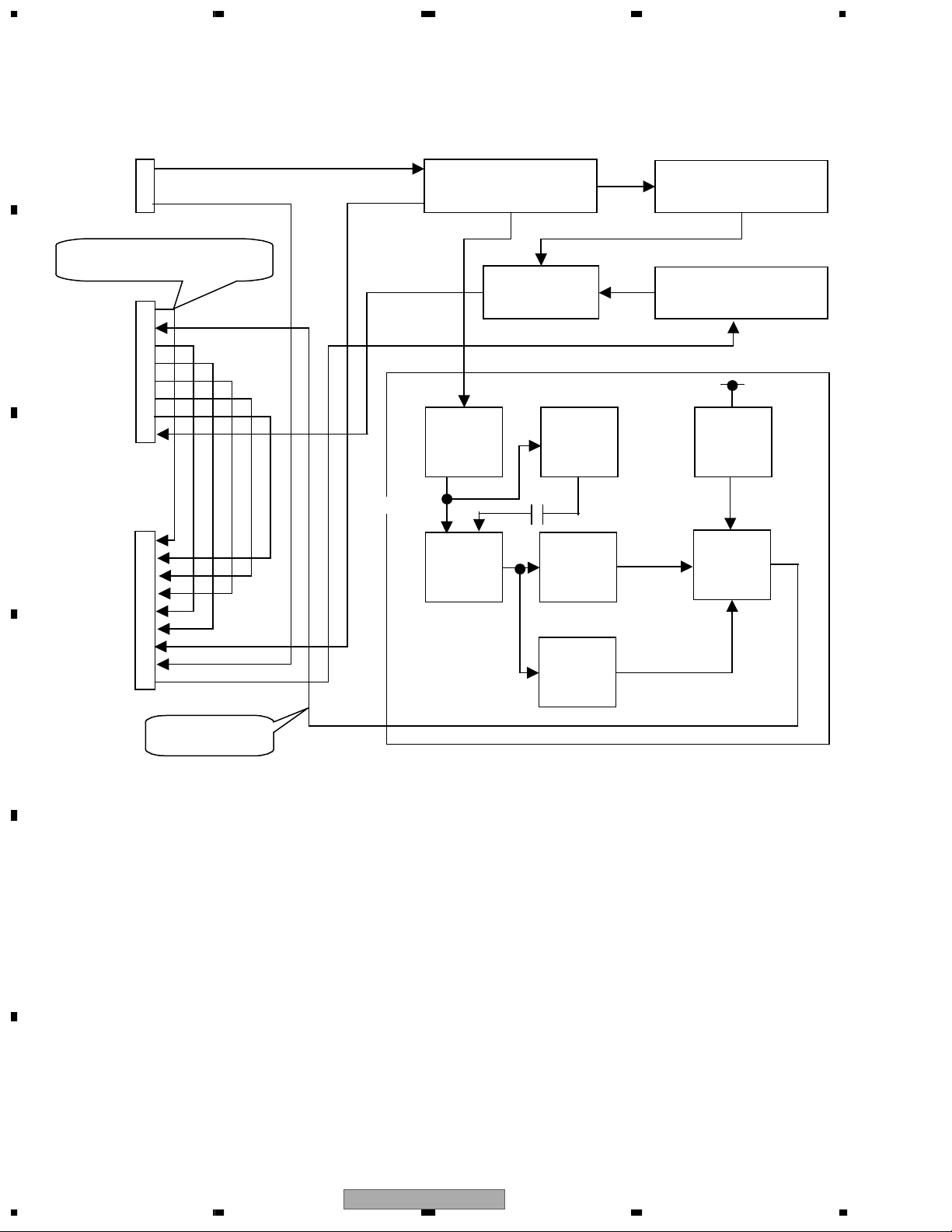
1234
3.1.6 SUB ADDRESS A and B ASSYS
A
+60V
ADRGND
CN8801
H : V MID CLAMP OFF
L : V MID CLAMP ON
B
C
D
V MID SW
ADRK EMG1
+12V
DGND
ADR-B ADR EMG 1 Block
ADR-U
ADR-D
ADRK. PD
CN8802
(DC+AC) (-AC) 5V
SW
ADR-D
ADR-U
ADR-B
+12V
DGND
VADR
ADRGND
ADROUT
CN8803
H : EMG1 OFF
L : EMG1 ON
Current - Voltage
Convert Block
R8801 - R8805 Q8801
P.D. Output Block
Q8803, Q8831 Q8805, Q8806
BUFF Block
IC8801 IC8801 D8804
Additional
Block
IC8802 IC8802 IC8803
(DC) CLK
Inversion
Block
Conparator
(EMG : ON)
Conparator
(EMG : OFF)
IC8804
Over Current DET. Block
ADR Output
Resistance Load Block
+5V REG
Flip / Flop
CLR
12V
E
F
38
PDP-503PC
1234
Page 39
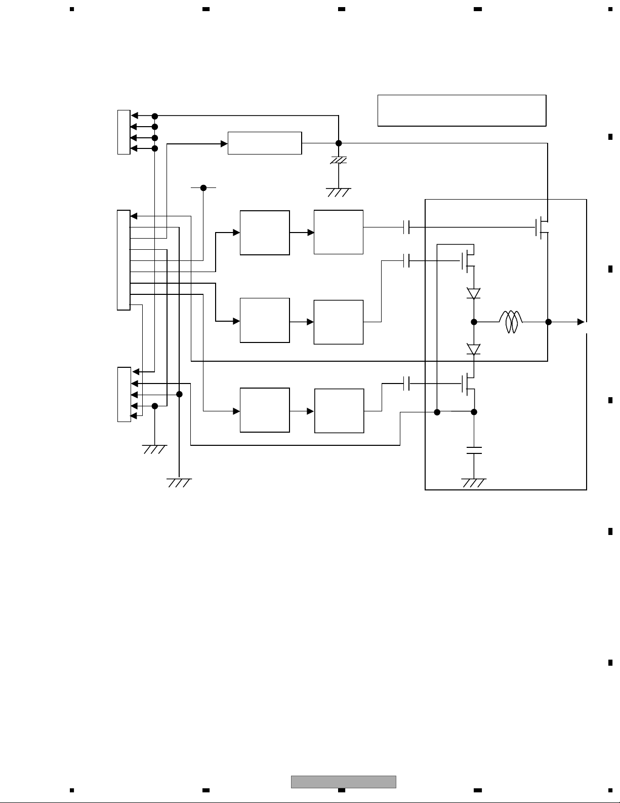
5678
+60V
+60V
+60V
+60V
CN6702 IC6704 C6703 - C6708
12V
Address Resonance Output Block
ADROUT
ADRGND
ADR B
VADR
C6720 Q6706
DGND
Q6707
+12V
IC6701 Q6701, Q6704 ADR U
ADR-B
C6721 Q6708
ADR-U
Q6709
ADR-D
SW
CN6701
ADR OUT
L6704
IC6702 Q6702, Q6705
VADR
V MID
ADR D
ADRGND
C6722 Q6710
DGND
Q6711
SW
CN6703
DGND IC6703 Q6703, Q6712 V MID
C6716
C6718
ADRGND
ICP-S1, 0
ADR-B
Pre-Drive
ADR-U
Pre-Drive
ADR-U
Drive
ADR-D
Pre-Drive
ADR-D
Drive
ADR-B
Drive
CAUTION :
FOR CONTINUED PROTECTION AGAINST RISK OF FIRE.
REPLACE ONLY WITH SAME TYPE NO. ICP-S1.0 MFD
BY ROHM CO., LTD. FOR IC6704.
3.1.7 ADR RESONANCE ASSY
A
B
C
D
E
56
PDP-503PC
F
7
8
39
Page 40

1234
3.1.8 ADR CONNECT A, B, C and D ASSYS
A
Address Module
(TCP)
Address Module
(TCP)
Address Module
(TCP)
Address Module
(TCP)
Address Module
(TCP)
ADR OUT
ADR PD
BRIDGE ASSY
OPEN PD
HZ
LBLK
HBLK
LE
HZ
LBLK
HBLK
LE
CLK
CLK
B
DATA_R
DATA_G
DATA_B
DATA_R
DATA_G
DATA_B
DATA_R
DATA_G
DATA_B
DATA_R
DATA_G
DATA_B
DATA_R
DATA_G
DATA_B
DATA_R
DATA_G
DATA_B
DATA_R
DATA_G
DATA_B
DATA_R
DATA_G
DATA_B
DATA_R
DATA_G
DATA_B
DATA_R
DATA_G
DATA_B
CN6501
Q6502, Q6503
Buffer
IC6501
C
D
E
F
40
1234
PDP-503PC
Page 41
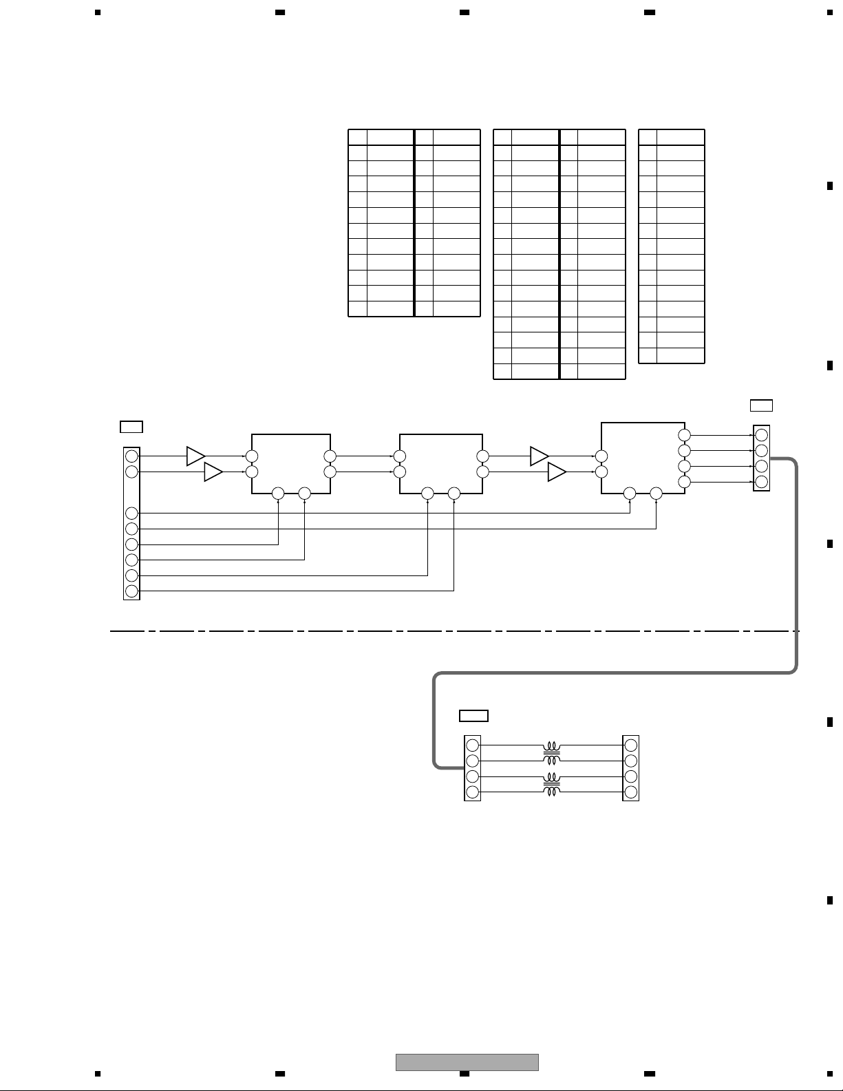
3.1.9 AUDIO AMP and SP TERMINAL ASSYS
4 22
1
14
11 12
96
8
7
11
12
13
14
A24
L
R
STB SW
CN5001
IC5202
(CXA2021S)
Audio Pre-Amp.
A_MUTE
SCL
SDA
FOCUS
SRS
AUDIO AMP ASSY
SP TERMINAL ASSY
30
1
L
R
IC5201
(NJM2193L)
Focus & SRS
Audio Processor
IC5002
(LA4628)
Audio
Power Amp.
19
12
1
6
L
R+
R–
L+
L–
R
17 18 4 5
2
3
5
6
8
9
11
13
A22
J5003
R+
L5301
ATF1206
L5352
ATF1206
R–
L+
L–
2
3
5
6
4
3
1
2
SP21
CN5302 CN5301
SPEAKER
TERMINAL
IC5201 (NJM2193L)IC5202 (CXA2021S) IC5002 (LA4628)
No. Voltage (V) No. Voltage (V)
1 5.9 12 5.25
2 0 13 1.73
3 5.95 14 5.95
4 5.94 15 5.92
5 5.98 16 5.91
6 6.02 17 5.93
7 6.02 18 5.92
8 7.38 19 5.94
9 5.95 20 5.95
10 1.55 21 11.91
11 5.24 22 5.9
No. Voltage (V) No. Voltage (V)
1 5.95 16 11.91
2 5.94 17 0
3 5.84 18 0
4 5.98 19 5.98
5 5.98 20 5.91
6 5.97 21 5.97
7 5.98 22 5.98
8 5.98 23 5.98
9 5.98 24 5.98
10 5.97 25 5.97
11 5.97 26 5.98
12 5.98 27 5.98
13 5.96 28 5.84
14 5.98 29 5.94
15 0 30 5.95
No. Voltage (V)
1 1.6
2 7.5
30
4 3.37
5 2.29
6 1.6
7 1.97
8 7.3
9 7.3
10 0
11 7.3
12 0
13 7.3
14 15
5678
A
B
C
D
E
56
PDP-503PC
F
7
8
41
Page 42
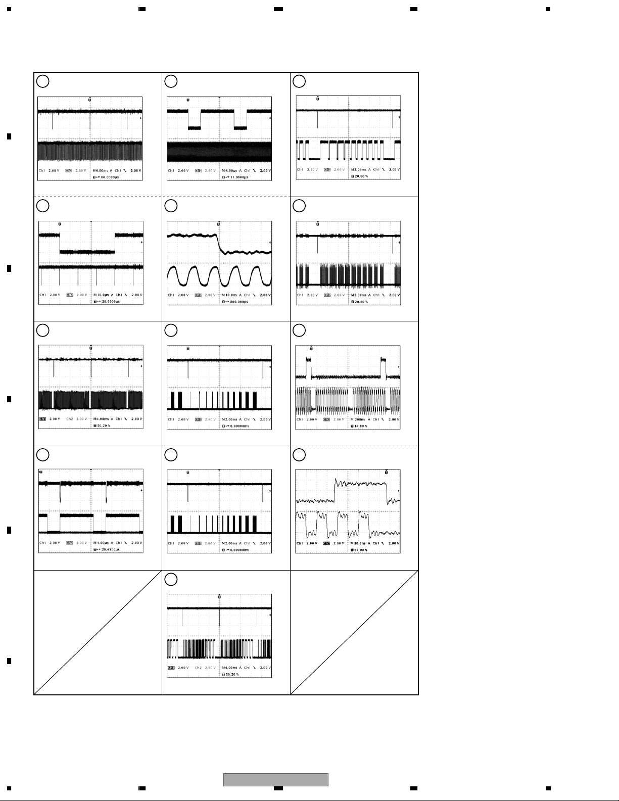
1234
3.2 WAVEFORMS
DIGITAL VIDEO ASSY
A
K1327 (VDI)
1
K1328 (HDI)
V: 2V/div. H: 4msec/div.
K1326 (DEI)
4
K1333 (VCLKL)
V: 2V/div. H: 4µsec/div.
K1308 (VDRB)
8
IC1501 - pin 15 (LBLK)
V: 2V/div. H: 2msec/div.
B
C
D
K1327 (VDI)
1
K1328 (HDI)
V: 2V/div. H: 10µsec/div.
K1327 (VDI)
2
CN1004 pin 49 (R DIGITAL VIDEO)
V: 2V/div. H: 4msec/div.
K1328 (HDI)
3
K1326 (DEI)
V: 2V/div. H: 4µsec/div.
K1326 (DEI)
4
K1333 (VCLKL)
V: 2V/div. H: 10nsec/div.
K1308 (VDRB)
5
R1713 - pin 7 (XSUS_B)
V: 2V/div. H: 2msec/div.
K1308 (VDRB)
6
R1703 - pin 8 (YSUS_B)
V: 2V/div. H: 2msec/div.
K1308 (VDRB)
9
IC1501 - pin 13 (LE)
V: 2V/div. H: 2msec/div.
IC1501 - pin 13 (LE)
10
IC1501 - pin 11 (ADRCLK)
V: 2V/div. H: 200nsec/div.
IC1501 - pin 13 (LE)
10
IC1501 - pin 11 (ADRCLK)
V: 2V/div. H: 20nsec/div.
K1308 (VDRB)
7
R1343 - pin 8 (RDAT_DL0)
E
V: 2V/div. H: 4msec/div.
F
42
PDP-503PC
1234
Page 43
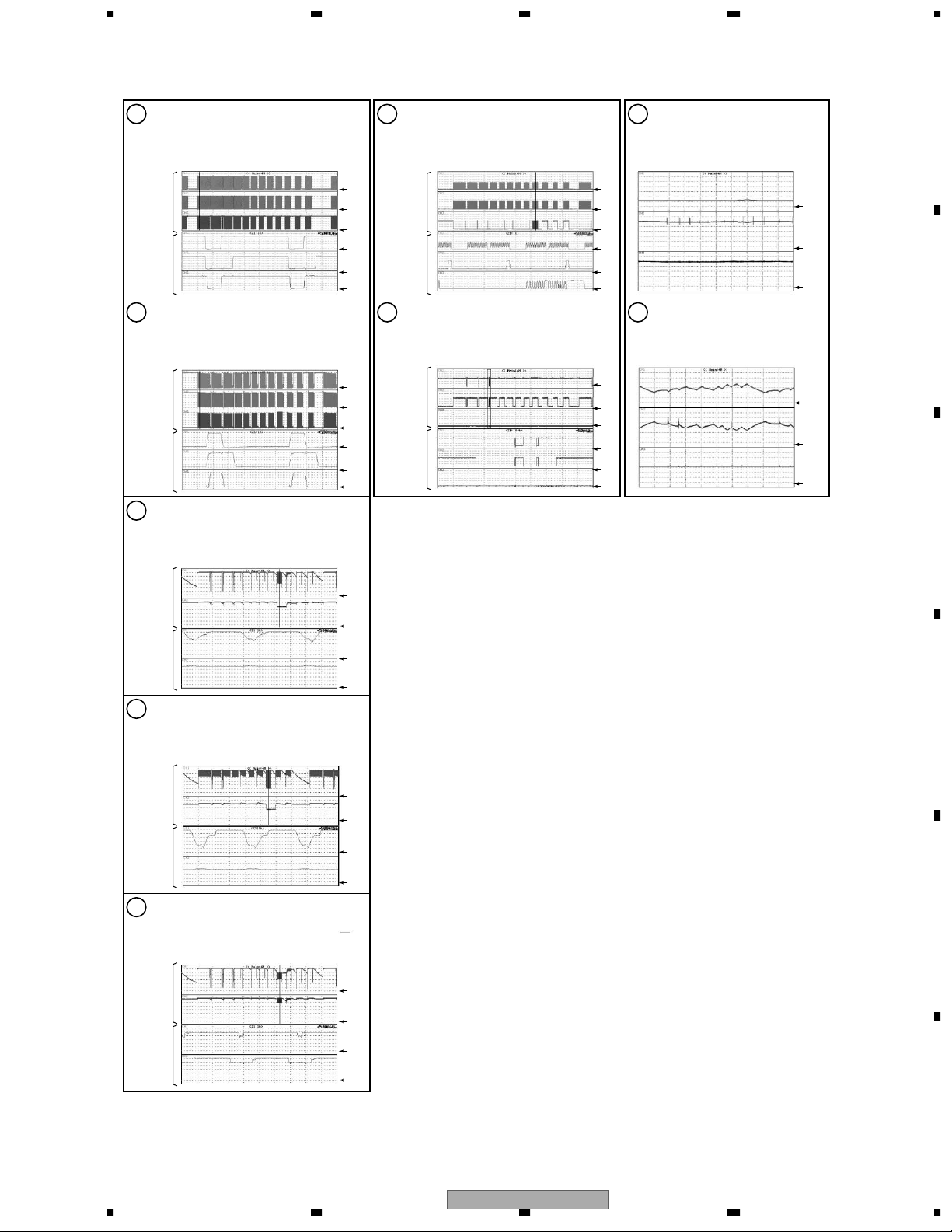
ADR RESONANCE ASSY
4
CH1 : Q6706 Drain
CH2 : Q6710 Soruse
V: 10V/div.
(Input : PC, Signal : Color bar)
3
CH1 : Q6706 Drain
CH2 : Q6710 Soruse
V: 10V/div.
(Input : VIDEO, Signal : Color bar)
2
CH1 : D6706 Cathode
CH2 : D6703 Cathode
CH3 : D6708 Cathode
V: 2V/div.
(Input : VIDEO, Signal : Color bar)
1
CH1 : IC6702 - pin 2
CH2 : IC6701 - pin 2
CH3 : IC6703 - pin 2
V: 1V/div.
(Input : VIDEO, Signal : Color bar)
ADR CONNECT A - D
ASSY
2
CH1 : IC6501 - pin 5 (HBLK)
CH2 : IC6501 - pin 3 (LBLK)
CH3 : IC6501 - pin 2 (HZ)
V: 1V/div.
(Input : VIDEO, Signal : Color bar)
1
CH1 : IC6501 - pin 8 (CLK)
CH2 : IC6501 - pin 6 (LE)
CH3 : IC6501 - (DATA)
V: 1V/div.
(Input : VIDEO, Signal : Color bar)
5
CH1 : Q6708 Drain
CH2 : Q6710 Drain
V: 10V/div.
(Input : VIDEO, Signal : Color bar)
SUB ADDRESS A, B
ASSY
2
CH1 : IC8801 - pin 3
CH2 : IC8801 - pin 7
CH3 : IC8802 - pin 1
V: 2V/div. H: 2msec/div.
(Input : VIDEO, Signal : Color bar)
1
CH1 : IC8801 - pin 3
CH2 : IC8801 - pin 7
CH3 : IC8802 - pin 1
V: 2V/div. H: 2msec/div.
(Input : VIDEO, Signal : Color bar)
CH1
H :
2msec/div
CH2
CH3
V MID CLAMP ASSY
2
CH1 : Q9006 Base (CLAMP REF V)
CH2 : D9010 Anode (MID)
CH3 : Q9006 Collector
V: 10V/div. H: 2msec/div.
(Input : PC, Signal : Color bar)
1
CH1 : Q9006 Base (CLAMP REF V)
CH2 : D9010 Anode (MID)
CH3 : Q9006 Collector
V: 10V/div. H: 2msec/div.
(Input : VIDEO, Signal : Color bar)
CH1
CH2
CH3
CH1
CH2
CH1
CH2
CH1
CH2
CH1
CH2
CH1
CH2
CH1
CH2
H :
500nsec/div
H :
2msec/div
H :
500nsec/div
H :
2msec/div
H :
500nsec/div
H :
2msec/div
H :
500nsec/div
H :
2msec/div
H :
500nsec/div
H :
2msec/div
H :
500nsec/div
H :
2msec/div
H :
500nsec/div
GND
GND
GND
GND
GND
GND
CH1
CH2
CH3
CH1
CH2
CH3
GND
CH1
CH2
CH3
GND
GND
GND
CH1
CH2
CH3
GND
GND
GND
CH1
CH1
CH2
CH2
CH3
CH3
GND
GND
GND
GND
GND
GND
GND
GND
GND
GND
GND
CH1
CH2
CH3
CH1
CH2
CH3
GND
GND
GND
GND
GND
GND
CH1
CH2
CH3
CH1
CH2
CH3
GND
GND
GND
GND
GND
GND
GND
GND
GND
GND
GND
GND
GND
GND
GND
GND
GND
GND
5678
A
B
C
D
E
PDP-503PC
56
F
7
8
43
Page 44
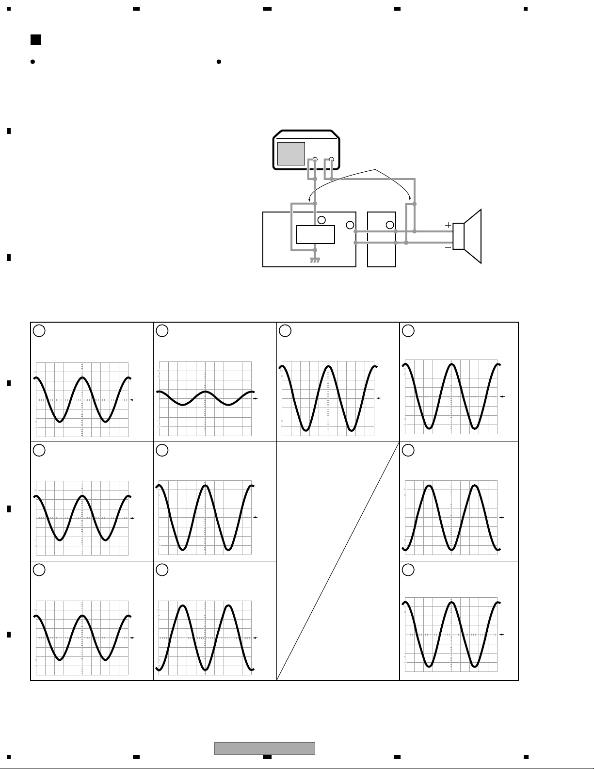
1234
AUDIO SECTION
A
Measurement condition
Video Input Signal : FULL FIELD COLOR-BAR
Audio Input Signal : 1kHz Sine Carve 0.2Vrms
Volume : 60 (MAX)
AV Selection : STANDARD
SRS : OFF
Caution in the measurement
Audio Power Amp. (IC5002: LA4628) on the AUDIO AMP Assy is BTL system, and,
as for the power amplifier and the speaker output, ± poles becomes hot for the
ground. Therefore be careful not to connect the measuring instrument as the following
figures. (Power amplifier may be damaged.)
FOCUS : OFF
Oscilloscope
CH1 CH2
GND and the speaker output (- side) becomes
a short state on the oscilloscope.
B
1
Measurement
Point
AUDIO AMP
ASSY
etc.
7
10
SP TERMINAL
ASSY
Wrong connection example
AUDIO AMP ASSY SP TERMINAL ASSY
C
CN5001 - pin 4 (L) ↔ GND
1
V: 0.1V/div. H: 0.2msec/div.
IC5002 - pin 1 (IN1) ↔ GND
4
V: 0.1V/div. H: 0.2msec/div.
J5003 - pin 5 (L+) ↔ pin 6 (L–)
7
V: 2V/div. H: 0.2msec/div.
CN5301 - pin 1 (L+) ↔ GND
8
V: 1V/div. H: 0.2msec/div.
Speaker
4.4V
D
E
IC5202 - pin 14 (LOUT) ↔ GND
2
V: 0.1V/div. H: 0.2msec/div.
IC5201 - pin 19 (FOCUSOUTL) ↔ GND
3
V: 0.1V/div. H: 0.2msec/div.
5.8V
5.9V
J5003 - pin 5 (L+) ↔ GND
5
V: 1V/div. H: 0.2msec/div.
J5003 - pin 6 (L–) ↔ GND
6
V: 1V/div. H: 0.2msec/div.
1.6V
7.3V
7.3V
0V
CN5301 - pin 2 (L–) ↔ GND
9
V: 1V/div. H: 0.2msec/div.
CN5301 - pin 1 (L+) ↔ pin 2 (L–)
10
V: 2V/div. H: 0.2msec/div.
7.3V
7.3V
0V
F
44
PDP-503PC
1234
Page 45

Sustain Waveforms
Sustain Waveform (1 field)
Drive Pulse Waveforms
ch 1 : K3107 (X.PSUS) - K3201 (SUSGND)
V: 100V/div. H: 2msec/div.
ch 2 : K2220 (Y.PSUS) - K2219 (SUSGND)
V: 100V/div. H: 2msec/div.
Sustain Waveform
ch 1 : K2220 (Y.PSUS) - K2219 (SUSGND)
V: 100V/div. H: 500nsec/div.
ch 2 : K2028 (YSUS_U) - K2024 (DGND)
V: 10V/div. H: 500nsec/div.
ch 3 : K2027 (YSUS_B) - K2024 (DGND)
V: 10V/div. H: 500nsec/div.
ch 4 : K2029 (YSUS_D) - K2024 (DGND)
V: 10V/div. H: 500nsec/div.
ch 5 : K2037 (YSUS_G) - K2024 (DGND)
V: 10V/div. H: 500nsec/div.
Sustain Waveform (1 field)
ch 1 : K3107 (X.PSUS) - K3201 (SUSGND)
V: 50V/div. H: 1µsec/div.
ch 2 : K2220 (Y.PSUS) - K2219 (SUSGND)
V: 50V/div. H: 1µsec/div.
Sustain Waveform (1 sub-field)
ch 1 : K3107 (X.PSUS) - K3201 (SUSGND)
V: 100V/div. H: 500µsec/div.
ch 2 : K2220 (Y.PSUS) - K2219 (SUSGND)
V: 100V/div. H: 500µsec/div.
Sustain Waveform (sustain)
ch 1 : K3107 (X.PSUS) - K3201 (SUSGND)
V: 50V/div. H: 5µsec/div.
ch 2 : K2220 (Y.PSUS) - K2219 (SUSGND)
V: 50V/div. H: 5µsec/div.
Sustain Waveform (sustain)
ch 1 : K3107 (X.PSUS) - K3201 (SUSGND)
V: 50V/div. H: 2µsec/div.
ch 2 : K2220 (Y.PSUS) - K2219 (SUSGND)
V: 50V/div. H: 2µsec/div.
Sustain Waveform (reset pulse)
ch 1 : K3107 (X.PSUS) - K3201 (SUSGND)
V: 100V/div. H: 5µsec/div.
ch 2 : K2220 (Y.PSUS) - K2219 (SUSGND)
V: 100V/div. H: 5µsec/div.
Y Drive Pulse Control Waveform
(1 field)
ch 1 : K2220 (Y.PSUS) - K2219 (SUSGND)
V: 100V/div. H: 2msec/div.
ch 2 : K2039 (YCP_MSK) - K2024 (DGND)
V: 10V/div. H: 2msec/div.
ch 3 : K2040 (YSUS_MSK) - K2024 (DGND)
V: 10V/div. H: 2msec/div.
ch 4 : K2041 (OFS) - K2024 (DGND)
V: 10V/div. H: 2msec/div.
ch 5 : K2053 (SOFT_D) - K2024 (DGND)
V: 10V/div. H: 2msec/div.
Y Drive Pulse Control Waveform
(1 sub-field)
ch 1 : K2220 (Y.PSUS) - K2219 (SUSGND)
V: 100V/div. H: 50µsec/div.
ch 2 : K2039 (YCP_MSK) - K2024 (DGND)
V: 10V/div. H: 50µsec/div.
ch 3 : K2040 (YSUS_MSK) - K2024 (DGND)
V: 10V/div. H: 50µsec/div.
ch 4 : K2041 (OFS) - K2024 (DGND)
V: 10V/div. H: 50µsec/div.
ch 5 : K2053 (SOFT_D) - K2024 (DGND)
V: 10V/div. H: 50µsec/div.
X Drive Pulse Control Waveform
(1 field)
ch 1 : K3107 (X.PSUS) - K3201 (SUSGND)
V: 100V/div. H: 2msec/div.
ch 2 : K3017 (XCP_MSK) - K3005 (DGND)
V: 10V/div. H: 2msec/div.
ch 3 : K3015 (XSUS_MSK) - K3005 (DGND)
V: 5V/div. H: 2msec/div.
5678
A
B
C
D
E
56
PDP-503PC
F
7
8
45
Page 46

1234
5.PCB PARTS LIST
A
NOTES:
Parts marked by "NSP" are generally unavailable because they are not in our Master Spare Parts List.
The mark found on some component parts indicates the importance of the safety factor of the part.
Therefore, when replacing, be sure to use parts of identical designation.
When ordering resistors, first convert resistance values into code form as shown in the following examples.
Ex.1 When there are 2 effective digits (any digit apart from 0), such as 560 ohm and 47k ohm (tolerance is shown by J=5%,
and K=10%).
560 Ω
47k Ω
0.5 Ω
1 Ω
56 x 10
47 x 10
R50
1R0
Ex.2 When there are 3 effective digits (such as in high precision metal film resistors).
5.62k Ω
B
Mark No. Description Part No.
LIST OF ASSEMBLIES
NSP 1..SCAN FUKUGO ASSY AWV1968
2..SCAN (A) ASSY AWZ6722
2..SCAN (B) ASSY AWZ6723
2..X CONNECTOR (A) ASSY AWZ6732
2..X CONNECTOR (B) ASSY AWZ6733
2..BRIDGE A ASSY AWZ6734
2..BRIDGE B ASSY AWZ6735
2..BRIDGE C ASSY AWZ6736
2..BRIDGE D ASSY AWZ6737
2..CLAMP A ASSY AWZ6738
2..CLAMP B ASSY AWZ6739
C
2..CLAMP C ASSY AWZ6740
2..CLAMP D ASSY AWZ6741
NSP 1..ADDRESS FUKUGO ASSY AWV1900
NSP 2..ADR CONNECT A ASSY AWZ6626
NSP 2..ADR CONNECT B ASSY AWZ6627
NSP 2..ADR CONNECT C ASSY AWZ6628
NSP 2..ADR CONNECT D ASSY AWZ6629
2..ADR RESONANCE ASSY AWZ6750
1..X DRIVE ASSY AWV1901
NSP 1..HD Y DRIVE ASSY AWV1949
D
2..Y DRIVE ASSY AWZ6707
2..SUB ADDRESS A ASSY AWZ6689
2..SUB ADDRESS B ASSY AWZ6690
2..SENSOR ASSY AWZ6696
1..DIGITAL VIDEO ASSY AWV1979
NSP 1..HD FUKUGO ASSY AWV1952
2.. LED ASSY AWZ6655
2..FRONT KEY ASSY AWZ6656
2..FRONT KEY CONNECT ASSY AWZ6657
2..IR RECEIVE (P) ASSY AWZ6658
2..MR INTERFACE ASSY AWZ6699
E
NSP 1..HD AUDIO ASSY AWV1935
2..AUDIO AMP ASSY AWZ6687
2..SP TERMINAL ASSY AWZ6688
F
46
1234
1
3
561
473
RD1/4PU J
RD1/4PU J
RN2H K
RS1P K
1
5621
RN1/4PC F562 x 10
561
473
R50
1R0
5621
Mark No. Description Part No.
SCAN (A) ASSY
SEMICONDUCTORS
IC6201-IC6206 SN755864APZP
D6207 KU10N16
CAPACITORS
C6201, C6202, C6212, C6213 (0.1/250V)ACG1088
C6222, C6223, C6232, C6233 (0.1/250V)ACG1088
C6242, C6243, C6252, C6253 (0.1/250V)ACG1088
C6203, C6259 CCSRCH151J50
C6206, C6210, C6215, C6219, C6227 CCSRCH181J50
C6229, C6236, C6240, C6244, C6246 CCSRCH181J50
C6255, C6260 CCSRCH181J50
C6208, C6209, C6217, C6218, C6226 CCSRCH331J50
C6230, C6238, C6239, C6245, C6250 CCSRCH331J50
C6257, C6258 CCSRCH331J50
C6204, C6205, C6207, C6214, C6216 CCSRCH390J50
C6220, C6224, C6225, C6231 CCSRCH390J50
C6234, C6235, C6237, C6248, C6249 CCSRCH390J50
C6251, C6254, C6256, C6262-C6266 CCSRCH390J50
C6211, C6221, C6228, C6241, C6247 CKSRYF104Z16
C6261 CKSRYF104Z16
RESISTORS
R6207, R6209, R6222, R6228, R6232 RAB4C221J
R6239 RAB4C221J
Other Resistors RS1/16S###J
O
THERS
CN6201 (15P COONNECTOR) AKP1218
K6202, K6212, K6219, K6225, K6231 AKX9002
(TEST PIN)
K6239, K6244 (TEST PIN) AKX9002
SCAN (B) ASSY
PDP-503PC
SEMICONDUCT
IC6001-IC6006 SN755864APZP
D6007 KU10N16
CAP
ACITORS
C6001, C6002, C6011, C6012 (0.1/250V)ACG1088
C6021, C6022, C6031, C6032 (0.1/250V)ACG1088
C6041, C6042, C6051, C6052 (0.1/250V)ACG1088
C6004, C6058 CCSRCH151J50
C6005, C6009, C6013, C6015 CCSRCH181J50
C6026, C6027, C6038, C6040, C6044 CCSRCH181J50
C6048, C6054, C6059 CCSRCH181J50
ORS
Page 47

5678
Mark No. Description Part No.
C6007, C6008, C6014, C6019, C6025 CCSRCH331J50
C6028, C6035, C6039, C6046, C6047 CCSRCH331J50
C6056, C6057 CCSRCH331J50
C6003, C6006, C6017, C6018, C6020 CCSRCH390J50
C6023, C6024, C6029, C6033, C6034 CCSRCH390J50
C6037, C6043, C6045, C6049, C6053 CCSRCH390J50
C6055, C6060, C6062-C6066 CCSRCH390J50
C6010, C6016, C6030, C6036, C6050 CKSRYF104Z16
C6061 CKSRYF104Z16
RESISTORS
R6007, R6012, R6021, R6028, R6032 RAB4C221J
R6040 RAB4C221J
Other Resistors RS1/16S###J
OTHERS
CN6001 (15P CONNECTOR) AKP1218
K6001, K6012, K6018, K6025, K6031 AKX9002
(TEST PIN)
K6038, K6044 (TEST PIN) AKX9002
X CONNECTOR (A) ASSY
RESISTORS
All Resistors RS1/16S###J
X CONNECTOR (B) ASSY
RESISTORS
All Resistors RS1/16S###J
Mark No. Description Part No.
BRIDGE D ASSY
SEMICONDUCTORS
D6451 D1FL20U(S)
CAPACITORS
C6451 (0.1/100V) ACG1098
OTHERS
CN6451 (4P PH CONNECTOR) B4B-PH-SM3
CLAMP A ASSY
SEMICONDUCTORS
D6461 D1FL20U(S)
CAPACITORS
C6461 (0.1/100V) ACG1098
OTHERS
CN6461 (4P PH CONNECTOR) B4B-PH-SM3
CLAMP B ASSY
SEMICONDUCTORS
D6471 D1FL20U(S)
CAPACITORS
C6471 (0.1/100V) ACG1098
OTHERS
CN6471 (4P PH CONNECTOR) B4B-PH-SM3
A
B
C
BRIDGE A ASSY
SEMICONDUCTORS
D6421 D1FL20U(S)
CAPACITORS
C6421 (0.1/100V) ACG1098
OTHERS
CN6421 (4P PH CONNECTOR) B4B-PH-SM3
BRIDGE B ASSY
SEMICONDUCTORS
D6431 D1FL20U(S)
CAP
ACITORS
C6431 (0.1/100V) ACG1098
O
THERS
CN6431 (4P PH CONNECTOR) B4B-PH-SM3
BRIDGE C ASSY
SEMICONDUCTORS
D6441 D1FL20U(S)
CAPACITORS
C6441 (0.1/100V) ACG1098
OTHERS
CN6441 (4P PH CONNECTOR) B4B-PH-SM3
CLAMP C ASSY
SEMICONDUCTORS
D6481 D1FL20U(S)
CAPACITORS
C6481 (0.1/100V) ACG1098
OTHERS
CN6481 (4P PH CONNECTOR) B4B-PH-SM3
CLAMP D ASSY
SEMICONDUCTORS
D6491 D1FL20U(S)
CAPACITORS
C6491 (0.1/100V) ACG1098
OTHERS
CN6491 (4P PH CONNECTOR) B4B-PH-SM3
ADR CONECT A ASSY
SEMICONDUCTORS
IC6501 TC74VHC541FT
Q6502 2SC2712
Q6503 2SK209
D6501 DA227
COILS AND FILTERS
L6501, L6502 ATH1081
D
E
F
56
PDP-503PC
7
8
47
Page 48

1234
Mark No. Description Part No.
CAPACITORS
C6511-C6520 (330p/100V) ACG1105
A
C6531, C6533, C6534 (47/6.3V) ACH1341
C6536-C6538 CCSRCH121J50
C6506-C6510, C6521-C6525, C6532 CKSRYF104Z16
C6535 CKSRYF104Z16
RESISTORS
R6518-R6522, R6524, R6526, R6528 RAB4C100J
R6530, R6531, R6533-R6537, R6539 RAB4C100J
R6541, R6543, R6545, R6547 RAB4C100J
R6516 RAB4C473J
Other Resistors RS1/16S###J
OTHERS
B
CN6501 (55P CONNECTOR) AKM1202
ADR CONECT B ASSY
SEMICONDUCTORS
IC6601 TC74VHC541FT
Q6602 2SC2712
Q6603 2SK209
D6601 DA227
COILS AND FILTERS
C
D
L6601, L6602 ATH1081
CAPACITORS
C6611-C6620 (330p/100V) ACG1105
C6631, C6633, C6634 (47/6.3V) ACH1341
C6636-C6638 CCSRCH121J50
C6606-C6610, C6621-C6625, C6632 CKSRYF104Z16
C6635 CKSRYF104Z16
RESISTORS
R6618-R6622, R6624, R6626, R6628 RAB4C100J
R6630, R6631, R6633-R6637, R6639 RAB4C100J
R6641, R6643, R6645, R6647 RAB4C100J
R6616 RAB4C473J
Other Resistors RS1/16S###J
Mark No. Description Part No.
Other Resistors RS1/16S###J
OTHERS
CN6801 (55P CONNECTOR) AKM1202
ADR CONNECT D ASSY
SEMICONDUCTORS
IC6901 TC74VHC541FT
Q6902 2SC2712
Q6903 2SK209
D6901 DA227
COILS AND FILTERS
L6901, L6902 ATH1081
CAPACITORS
C6911-C6920 (330p/100V) ACG1105
C6931, C6933, C6934 (47/6.3V) ACH1341
C6936-C6938 CCSRCH121J50
C6906-C6910, C6921-C6925, C6932 CKSRYF104Z16
C6935 CKSRYF104Z16
RESISTORS
R6918-R6922, R6924, R6926, R6928 RAB4C100J
R6930, R6931, R6933-R6937, R6939 RAB4C100J
R6941, R6943, R6945, R6947 RAB4C100J
R6916 RAB4C473J
Other Resistors RS1/16S###J
OTHERS
CN6901 (55P CONNECTOR) AKM1202
ADR RESONANCE ASSY
SEMICONDUCTORS
IC6704 (1A/50V) ICP-S1.0
>
IC6701-IC6703 TND301S
Q6704, Q6705, Q6712 2SB1132
Q6701-Q6703 2SD1664
Q6710, Q6711 2SK3483-Z
OTHERS
CN6601 (55P CONNECTOR) AKM1202
ADR CONNECT C ASSY
SEMICONDUCTORS
IC6801 TC74VHC541FT
Q6802 2SC2712
Q6803 2SK209
E
F
D6801 DA227
COILS AND FILTERS
L6801, L6802 ATH1081
CAPACITORS
C6811-C6820 (330p/100V) ACG1105
C6831, C6833, C6834 (47/6.3V) ACH1341
C6836-C6838 CCSRCH121J50
C6806-C6810, C6821-C6825, C6832 CKSRYF104Z16
C6835 CKSRYF104Z16
RESISTORS
R6818-R6822, R6824, R6826, R6828 RAB4C100J
R6830, R6831, R6833-R6837, R6839 RAB4C100J
R6841, R6843, R6845, R6847 RAB4C100J
R6816 RAB4C473J
48
1234
Q6706-Q6709 FX20ASJ-2
D6701, D6703, D6704, D6706 1SS355
D6709, D6710, D6717, D6718 D1FL20U(S)
D6711-D6714 SPX-62S
D6702, D6705, D6716 UDZ15B
COILS AND FILTERS
L6704 ATH1111
CAPACITORS
C6716 (2.0/250V) ACE1162
C6720, C6721 (0.01/100V) ACG1101
C6722 (0.0068F/100V) ACG1102
C6703-C6708 (56/80V) ACH1347
C6709 CEHV101M16
C6701, C6702 CEHV470M16
C6710, C6711, C6713 CKSRYF104Z16
RESISTORS
Other Resistors RS1/16S###J
OTHERS
CN6701 (23P CONNECTOR) AKP1221
CN6702 (4P CONNECTOR) B4B-PH-SM3
CN6703 (5P CONNECTOR) B5B-PH-SM3
PDP-503PC
Page 49
5678
Mark No. Description Part No.
X DRIVE ASSY
[X LOGIC BLOCK]
SEMICONDUCTORS
IC3003 PE1012A
IC3004 TC74ACT540FT
IC3001, IC3008 TC74ACT541FT
COILS AND FILTERS
L3001 LFEA100J
CAPACITORS
C3005 CEHAT470M16
C3001, C3003, C3004, C3006 CKSRYF104Z50
RESISTORS
R3009-R3012 RAB4C0R0J
R3001, R3003, R3026, R3029 RAB4C470J
R3002, R3005, R3030, R3033 RAB4C472J
Other Resistors RS1/16S###J
OTHERS
CN3001 (30P CONNECTOR) KF050HA30L
[X SUS BLOCK]
SEMICONDUCTORS
IC3102 HCPL-M611
IC3200, IC3201 STK795-460
IC3101 TC74ACT541FT
IC3103, IC3104, IC3106, IC3107, IC3110TND301S
IC3113 TND301S
IC3109 UPC78L05T
Q3116, Q3119, Q3120 2SJ522
Q3101 2SK2503
Q3103-Q3107, Q3109-Q3115 FS16VS-9
Q3124-Q3127 FS16VS-9
Q3122, Q3128 FS7VS-14A
Q3102 HN1B04FU
D3119 1SS184
D3108, D3124, D3125, D3133 1SS355
D3126, D3131, D3200, D3203, D3205 D1FL40
D3208, D3212-D3215 D1FL40
D3101, D3102, D3117, D3202, D3207 EC11FS4
D3210, D3211 EC11FS4
D3120, D3127-D3129, D3135, D3136 UDZ15B
COILS AND FILTERS
L3206, L3207 ATH1112
L3201, L3204 ATH1117
L3202, L3205, L3210, L3211 ATH1118
L3101 LFEA100J
L3107, L3108 LFEA101J
L3103 LFEA470J
Mark No. Description Part No.
C3104, C3106 CEHAT470M16
C3135 CEHAT470M25
C3137, C3138 CKSRYB473K25
C3103, C3105, C3108, C3109, C3111 CKSRYF104Z50
C3113, C3114, C3117, C3130, C3140 CKSRYF104Z50
RESISTORS
R3183, R3184, R3187 (15) ACN1156
R3113, R3114, R3121, R3122, R3126 RAB4C100J
R3132, R3140, R3141 RAB4C100J
R3212, R3217, R3230, R3234, R3237 RS1/10S184J
R3240, R3242, R3245 RS1/10S184J
R3250-R3253 RS1/16S3300F
R3134, R3163 RS1/2S100J
R3103 RS1/2S102J
R3109 RS1/2S2R2J
R3102 RS1/2S561J
R3215, R3216 RS1MMF101J
R3228, R3229 RS1MMF102J
R3178, R3179 RS3LMF121J
VR3200-VR3203 (1k) ACP1089
Other Resistors RS1/16S###J
OTHERS
3101 (SPACER) AEH1049
KN3105-KN3114 (GROUND PLATE) ANK-142
CN3101 (13P PLUG) KM250MA13
[X DD CON BLOCK]
SEMICONDUCTORS
IC3712 AN1431M
IC3701 MIP161
IC3702-IC3704 TLP181(GR)
Q3701 2SC2712
Q3800 HN1A01FU
D3710, D3711 1SS355
D3705, D3706 D1FL20U(S)
D3702 EC8FS6
D3708, D3709, D3713 RD110P
D3703 UDZ18B
D3707 UDZS5.6B
COILS AND FILTERS
L3701 ATH1110
T3701 ATK1153
CAPACITORS
C3701 (22/315V) ACH1345
C3717 (47/350V) ACH1346
C3704 CEHAT101M16
C3706, C3711, C3714 CEHAT101M25
C3712 CEHAT331M16
A
B
C
D
E
CAPACITORS
C3205, C3206, C3212, C3213(1.5/250V)ACE1160
C3225, C3226 (1.5/250V) ACE1160
C3139, C3143 (0.1/630V) ACG1092
C3223, C3224 (100P/630V) ACG1104
C3132 (47/350V) ACH1346
C3200-C3202, C3207-C3209 (330/280V)ACH1352
C3214-C3221 CCSRCH331J50
C3112, C3203, C3210 CEHAT101M16
C3102, C3107, C3115, C3204, C3211 CEHAT101M25
C3101 CEHAT221M25
56
RESISTORS
PDP-503PC
C3705 CKSQYF104Z50
C3703, C3707, C3708, C3710 CKSRYB104K16
C3715, C3716 CKSRYB104K16
R3732 RS1/16S1001F
R3806 RS1/16S1802F
R3701-R3704, R3706-R3717 RS1/16S1803F
R3805 RS1/16S2702F
R3731 RS1/16S3900F
R3802 RS1/16S5601F
7
8
F
49
Page 50

1234
Mark No. Description Part No.
R3738, R3739 RS1/2S102J
R3800, R3801 RS1/2S823J
A
VR3701 (1k) ACP1089
Other Resistors RS1/16S###J
Y DRIVE ASSY
[Y DRIVE LOGIC BLOCK]
SEMICONDUCTORS
IC2006 PE1013B
IC2007 TC74ACT540FT
IC2001, IC2003-IC2005 TC74ACT541FT
IC2101 TLP181(GR)
COILS AND FILTERS
B
C
D
E
F
L2001 LFEA100J
CAPACITORS
C2101 CEHAT100M50
C2003 CEHAT470M16
C2001, C2004, C2005, C2007, C2008 CKSRYF104Z50
C2010, C2102, C2104, C2122 CKSRYF104Z50
RESISTORS
R2015-R2018 RAB4C0R0J
R2001, R2002, R2005, R2011 RAB4C470J
R2037, R2038 RAB4C470J
R2035, R2036, R2039, R2040 RAB4C472J
Other Resistors RS1/16S###J
OTHERS
CN2001 (50P CONNECTOR) AKM1201
[Y DRIVE SUS BLOCK]
SEMICONDUCTORS
IC2202, IC2208 HCPL-M611
IC2206, IC2214 STK795-460
IC2201 TC74ACT541FT
IC2203,IC2204,IC2210,IC2212,IC2213 TND301S
IC2216, IC2217 TND301S
IC2205, IC2209 UPC78L05T
Q2203 2SJ281
Q2204, Q2205 2SJ522
Q2201 2SK2503
Q2215-Q2221, Q2226-Q2228 FQB34N20
Q2232, Q2233 FQB34N20
Q2210-Q2211 FS16VS-9
Q2209 HN1B04FU
D2225 1SS184
D2202, D2204 1SS226
D2211 1SS355
D2201 D1FL20U(S)
D2203, D2205, D2208, D2210, D2212 D1FL40
D2214-D2216, D2221-D2223 D1FL40
D2226-D2228, D2239, D2243 D1FL40
D2209 DF20L60
D2206, D2207 UDZ15B
COILS AND FILTERS
L2207 ATH1110
L2213, L2214 ATH1112
L2206, L2211 ATH1117
L2208, L2212, L2215, L2216 ATH1118
L2210 LFEA100J
Mark No. Description Part No.
L2201, L2204 LFEA470J
CAPACITORS
C2228, C2230, C2231, C2250-C2252 ACE1160
(1.5/250V)
C2209, C2210 (0.1/630V) ACG1092
C2233, C2248 (100p/630V) ACG1104
C2211 (47/350V) ACH1346
C2216, C2217, C2219, C2234-C2236 ACH1352
(330/280V)
C2253-C2260 CCSRCH331J50
C2221, C2225, C2226, C2246 CEHAT101M16
C2204, C2227, C2237, C2240, C2247 CEHAT101M25
C2202 CEHAT221M25
C2232 (220/16V) ACH1354
C2218, C2224, C2229 CEHAT470M16
C2212, C2214 CEHAT470M25
C2201, C2203, C2205, C2208, C2213 CKSRYF104Z50
C2220, C2222, C2223, C2238, C2239 CKSRYF104Z50
C2241, C2242 CKSRYF104Z50
RESISTORS
R2235, R2273, R2291, R2305, R2315 RAB4C100J
R2317, R2342 RAB4C100J
R2253, R2256, R2270, R2283, R2332 RS1/10S184J
R2338, R2354, R2355 RS1/10S184J
R2358-R2361 RS1/16S3300F
R2263, R2264 RS1/2S100J
R2203 RS1/2S102J
R2209 RS1/2S2R2J
R2202 RS1/2S561J
R2278, R2303 RS1MMF101J
R2233, R2234 RS1MMF102J
R2274, R2275 RS1MMF221J
R2298, R2299 RS2MMF4R7J
R2276, R2281 RS3LMFR82J
VR2201-VR2204 (1k) ACP1089
Other Resistors RS1/16S###J
OTHERS
2201 (SPACER) AEH1049
KN2201-KN2210 (GROUND PLATE) ANK-142
CN2201 (16P PLUG) KM250MA15
[Y DRIVE SCAN BLOCK]
SEMICONDUCTORS
IC2501,IC2502,IC2505,IC2510,IC2514 HCPL-M611
IC2504, IC2506 TC74ACT540FT
COILS AND FILTERS
L2501-L2503 LFEA100J
CAPACITORS
C2506, C2527 CEHAT220M2D
C2502 CEHAT221M16
C2524, C2525 CEHAT470M16
C2501, C2503, C2505, C2507, C2508 CKSRYF104Z50
C2513, C2517 CKSRYF104Z50
RESISTORS
R2502, R2504 RAB4C101J
Other Resistors RS1/16S###J
L2203, L2205 LFEA101J
50
1234
PDP-503PC
Page 51
5678
Mark No. Description Part No.
OTHERS
CN2501, CN2502 (15P CONNECTOR) AKM1200
[Y DRIVE DD-CON BLOCK]
SEMICONDUCTORS
IC2715-IC2717 AN1431M
IC2709 HCNR201
IC2708, IC2710, IC2718 M5223AFP
IC2711 MIP0223SC
IC2701 MIP161
IC2704 MIP301
IC2702, IC2703, IC2705-IC2707 TLP181(GR)
IC2712-IC2714 TLP181(GR)
Q2701, Q2703 2SC2712
Q2704 HN1A01FU
D2712, D2717, D2718, D2732, D2734 1SS355
D2736, D2737 1SS355
D2704, D2706, D2707, D2715, D2726 D1FL20U(S)
D2728 D1FL20U(S)
D2702, D2714, D2727 D1FL40
D2711 D1FS4
D2725 EC8FS6
D2733 RD91P
D2724 U1ZB330
D2713 U1ZB36
D2740 UDZ12B
D2709, D2716 UDZ3.6B
D2729, D2731 UDZ33B
D2703, D2710 UDZ36B
D2720, D2730, D2739 UDZS5.6B
COILS AND FILTERS
L2701 ATH1110
T2702 ATK1150
T2703 ATK1151
T2701 ATK1152
CAPACITORS
C2701, C2735 (22/315V) ACH1345
C2706, C2725, C2737 CEHAT101M16
C2709, C2718, C2720, C2739, C2745 CEHAT101M25
C2708 CEHAT101M2A
C2740 CEHAT101M2C
C2704 CEHAT221M25
C2715 CEHAT331M16
C2746 CEHAT331M25
C2723, C2751 CEHAT470M16
C2712 CEHAT471M35
C2711 CKSRYB103K50
C2705, C2713, C2714, C2719 CKSRYB104K16
C2721, C2722, C2724, C2727, C2729 CKSRYB104K16
C2731, C2733, C2736, C2742, C2743 CKSRYB104K16
C2747-C2749 CKSRYB104K16
C2728, C2730 CKSRYB471K50
C2707, C2738 CKSRYF104Z50
RESISTORS
R2735, R2791 RS1/16S1000F
R2780 RS1/16S1103F
R2715, R2728, R2733 RS1/16S1201F
R2787 RS1/16S1302F
R2766 RS1/16S1501F
Mark No. Description Part No.
R2785 RS1/16S1503F
R2777, R2786 RS1/16S1802F
R2776 RS1/16S2702F
R2705, R2706, R2709, R2710, R2778 RS1/16S3002F
R2781 RS1/16S3002F
R2783 RS1/16S4701F
R2734, R2736 RS1/16S4702F
R2779 RS1/16S5102F
R2773 RS1/16S5601F
R2784 RS1/16S5602F
R2782 RS1/16S6801F
R2744-R2746, R2748-R2753 RS1/16S9102F
R2711, R2716, R2767, R2770 RS1/2S102J
R2788, R2792 RS1/2S561J
R2771, R2772 RS1/2S823J
R2712 RS3LMF272J
VR2702, VR2703 (1k) ACP1089
VR2701 (2.2k) ACP1090
Other Resistors RS1/16S###J
OTHERS
2001, 3001 (SCREW) PMB30P060FNI
SUB ADDRESS A ASSY
SEMICONDUCTORS
IC8801, IC8802, IC8804 M5223AFP
IC8803 TC74VHC74FT
Q8802 2SA1163
Q8804, Q8805, Q8808 2SC2712
Q8806 2SK209
D8801-D8803, D8809 1SS355
D8806, D8807 DA227
D8808 UDZ27B
D8804 UDZS5.1B
COILS AND FILTERS
L8801 ATH1074
L8802, L8803 ATH1081
CAPACITORS
C8806 CCSRCH101J50
C8822 CEHV100M16
C8804 CEHV100M35
C8808 CEHV470M16
C8807 CEVNP2R2M35
C8802, C8805, C8809-C8817 CKSRYF104Z16
C8820, C8821 CKSRYF104Z16
RESISTORS
R8806, R8807, R8837, R8838, R8841 RS1/16S1002D
R8858 RS1/16S1202D
R8864 RS1/16S1802F
R8828, R8829, R8846 RS1/16S2202D
R8826, R8827, R8839, R8840 RS1/16S4701D
R8833, R8859 RS1/16S4702F
R8832 RS1/16S5602F
R8801, R8802 RS1/2S1R5J
R8803-R8805 RS1/2S2R2J
Other Resistors RS1/16S###J
OTHERS
CN8803 (23P CONNECTOR) AKM1205
CN8801 (3P PH CONNECTOR) S3B-PH-SM3
A
B
C
D
E
F
56
PDP-503PC
7
8
51
Page 52

1234
Mark No. Description Part No.
CN8802 (8P PH CONNECTOR) S8B-PH-SM3
A
SUB ADDRESS B ASSY
SEMICONDUCTORS
IC8901, IC8902, IC8904 M5223AFP
IC8903 TC74VHC74FT
Q8902 2SA1163
Q8904, Q8905, Q8908 2SC2712
Q8906 2SK209
D8901-D8903, D8909 1SS355
D8906, D8907 DA227
D8908 UDZ27B
B
D8904 UDZS5.1B
COILS AND FILTERS
L8901 ATH1074
L8902, L8903 ATH1081
CAPACITORS
C8906 CCSRCH101J50
C8922 CEHV100M16
C8904 CEHV100M35
C8908 CEHV470M16
C8907 CEVNP2R2M35
C
C8902, C8905, C8909-C8917 CKSRYF104Z16
C8920, C8921 CKSRYF104Z16
RESISTORS
R8906, R8907, R8937, R8938, R8941 RS1/16S1002D
R8958 RS1/16S1202D
R8964 RS1/16S1802F
R8928, R8929, R8946 RS1/16S2202D
R8926, R8927, R8939, R8940 RS1/16S4701D
R8933, R8959 RS1/16S4702F
R8932 RS1/16S5602F
R8901, R8902 RS1/2S1R5J
D
R8903-R8905 RS1/2S2R2J
Other Resistors RS1/16S###J
OTHERS
CN8903 (23P CONNECTOR) AKM1205
CN8901 (3P PH CONNECTOR) S3B-PH-SM3
CN8902 (8P PH CONNECTOR) S8B-PH-SM3
SENSOR ASSY
SEMICONDUCTORS
IC8351 LM50CIM3
E
IC8352 M5223AFP
Mark No. Description Part No.
DIGITAL VIDEO ASSY
[INTERFACE BLOCK]
SEMICONDUCTORS
IC1001-IC1008 TC74VHC541FT
COILS AND FILTERS
F1001-F1006 ATF1194
CAPACITORS
C1001-C1008 CKSRYF104Z16
RESISTORS
R1044 RAB4C101J
R1001-R1007, R1036, R1063-R1069 RAB4C103J
R1008-R1017, R1019, R1020, R1027 RAB4C470J
R1032, R1034, R1035, R1037, R1038 RAB4C470J
R1040-R1043, R1048, R1049 RAB4C470J
R1051-R1054 RAB4C470J
Other Resistors RS1/16S###J
OTHERS
CN1003, CN1004 (50P CONNECTOR) AKM1201
K1001 (TEST PIN) AKX9002
CN1001 (PH CONNECTOR) B12B-PH-SM3
[PANEL UCOM BLOCK]
SEMICONDUCTORS
IC1101 HD64F2328VF
IC1103 NC7SZ08P5
IC1102 PST9228N
Q1101, Q1103 DTC143EK
D1101 AEL1171
CAPACITORS
C1123, C1124 CCSRCH7R0D50
C1101 CEV101M4
C1102, C1109, C1110, C1112-C1116 CKSRYB102K50
C1129-C1132 CKSRYB102K50
C1117, C1121 CKSRYB103K50
C1120 CKSRYB472K50
C1103-C1108, C1111, C1118, C1119 CKSRYF104Z16
C1122, C1125-C1128 CKSRYF104Z16
RESISTORS
R1104, R1107, R1110, R1113, R1114 RAB4C472J
R1116, R1121, R1124, R1127, R1129 RAB4C472J
Other Resistors RS1/16S###J
OTHERS
K1101-K1104, K1107, K1108 (TEST PIN)AKX9002
X1101 (25MHz) ASS1160
CAPACITORS
RESISTORS
F
52
C8356 CEV470M6R3
C8354 CKSRYB103K50
C8351, C8355 CKSRYF104Z16
C8352, C8353 CKSRYF105Z10
R8354, R8358 RS1/16S1001F
Other Resistors RS1/16S###J
SEMICONDUCTORS
IC1204 24LC04B(I)SN
IC1207 M30624FGAFP
IC1208 PST9246N
IC1202 TC74VHC08FT
IC1201 TC74VHC21FT
IC1205 TC74VHC541FT
IC1203 TC74VHCT541AFT
IC1206 TC7W126FU
D1201, D1202 1SS355
PDP-503PC
1234
[MODULE UCOM BLOCK]
Page 53

5678
Mark No. Description Part No.
CAPACITORS
C1213, C1243-C1245 CCSRCH470J50
C1235, C1236 CCSRCH7R0D50
C1225, C1232 CEV470M6R3
C1201-C1203, C1206-C1211 CKSRYB102K50
C1214-C1216, C1218, C1219 CKSRYB102K50
C1223, C1224, C1226, C1227, C1229 CKSRYB102K50
C1237, C1238, C1241, C1242, C1247 CKSRYB102K50
C1234 CKSRYB103K50
C1233 CKSRYB472K50
C1204, C1205, C1212, C1217 CKSRYF104Z16
C1221, C1222, C1228, C1230, C1231 CKSRYF104Z16
C1239, C1240, C1246, C1248-C1250 CKSRYF104Z16
RESISTORS
R1209, R1214, R1245 RAB4C101J
R1242 RAB4C103J
R1207 RAB4C123J
R1213, R1216 RAB4C473J
Other Resistors RS1/16S###J
OTHERS
X1201 (16MHz) ASS1159
CN1203 (3P PH CONNECTOR) B3B-PH-SM3
CN1201, CN1202 (8P PLUG) CKS3130
[DIGITAL BLOCK]
SEMICONDUCTORS
IC1802 FS781BZB
IC1704 NC7SZ08P5
IC1301, IC1401 PD6358A
IC1703 PE5064A
IC1501, IC1502, IC1601, IC1602 TC74VCX541FT
IC1702, IC1801 TC74VHC541FT
IC1803 TC74VHC74FT
IC1701 TC74VHCT541AFT
D1301-D1305 1SS226
COILS AND FILTERS
F1301-F1304, F1501-F1505 ATF1194
F1601-F1605 ATF1194
Mark No. Description Part No.
OTHERS
CN1701 (50P CONNECTOR) AKM1201
CN1501, CN1502, CN1504, CN1505 AKM1202
(55P CONNECTOR)
CN1601, CN1602, CN1604, CN1605 AKM1202
(55P CONNECTOR)
K1301, K1302, K1308, K1311-K1314 AKX9002
(TEST PIN)
K1316, K1321, K1324, K1326-K1331 AKX9002
(TEST PIN)
K1333, K1501, K1502, K1601, K1602 AKX9002
(TEST PIN)
K1728, K1729 (TEST PIN) AKX9002
X1801 (50.000MHz) ASS1146
CN1503,CN1603(8P PH CONNECTOR) B8B-PH-SM3
CN1301 (8P PLUG) CKS3130
CN1702 (30P CONNECTOR) KF050HA30L
[D-D CONVERTER BLOCK]
SEMICONDUCTORS
Q1902, Q1905, Q1907 2SC2712
Q1903 DTC143EK
Q1901, Q1904, Q1906 HN1C01FU
D1903-D1906, D1911, D1912 1SS355
D1908 HZU2.2B
D1902, D1909 UDZ3.6B
D1907 UDZS5.1B
D1901 UDZS6.8B
CAPACITORS
C1904, C1906, C1912 CEV220M16
C1901-C1903, C1905, C1907-C1911 CKSRYF104Z16
RESISTORS
R1935, R1936 RS1/2S680J
Other Resistors RS1/16S###J
OTHERS
K1901-K1906 (TEST PIN) AKX9002
1901 (DC-DC CONVERTER) AXY1060
CN1901 (13P PH CONNECTOR) B13B-PH-SM3
A
B
C
D
CAPACITORS
C1807 CCSRCH271J50
C1802 CEV100M16
C1306, C1322, C1406, C1422, C1711 CEV101M4
C1806 CEV101M4
C1504-C1508, C1604-C1608, C1712 CKSRYB102K50
C1303-C1305, C1307-C1321 CKSRYF104Z16
C1323-C1336, C1403-C1405 CKSRYF104Z16
C1407-C1421, C1423-C1436, C1501 CKSRYF104Z16
C1503, C1601, C1603, C1701-C1710 CKSRYF104Z16
C1713, C1803-C1805 CKSRYF104Z16
RESISTORS
R1502, R1517, R1606, R1622 RAB4C101J
R1307, R1310-R1315, R1317, R1318 RAB4C220J
R1321, R1322, R1326-R1344, R1407 RAB4C220J
R1410-R1415, R1417, R1418 RAB4C220J
R1421, R1422, R1426-R1444 RAB4C220J
R1501, R1514, R1607, R1627, R1701 RAB4C470J
R1703-R1709, R1712-R1717 RAB4C470J
R1551, R1552 RS1/2S680J
Other Resistors RS1/16S###J
56
LED ASSY
SEMICONDUCTORS
D4751 AEL1170
OTHERS
CN4751 (3P CONNECTOR) S3B-PH-SM3
FRONT KEY ASSY
SWITCHES
S4801-S4806 ASG1088
CAPACITORS
C4801-C4803 CKSRYF104Z16
RESISTORS
Other Resistors RS1/16S###J
OTHERS
CN4801 (6P FFC CONNECTOR) AKM1208
PDP-503PC
E
F
7
8
53
Page 54

1234
Mark No. Description Part No.
FRONT KEY CONNCT ASSY
SEMICONDUCTORS
A
D4851, D4852 1SS226
OTHERS
CN4851 (6P FFC CONNECTOR) AKM1208
CN4852 (4P CONNECTOR) B4B-PH-SM3
IR RECEIVE (P) ASSY
SEMICONDUCTORS
Q4901 2SC2712
D4901 1SS355
B
CAPACITORS
C4901 CEV470M6R3
C4902 CKSRYB103K50
C4903 CKSRYB472K50
C4904 CKSRYF104Z16
RESISTORS
Other Resistors RS1/16S###J
OTHERS
REMO.RCEIVE UNIT GP1UM26RK
C
MR INTERFACE ASSY
[INTERFACE BLOCK]
SEMICONDUCTORS
IC4011 CXA1875AM
IC4007, IC4010 M5223AFP
IC4005 M62320FP
IC4001 PQ05DZ51
IC4002-IC4004 PQ20VZ1U
IC4013 PST9228N
IC4008, IC4009 TC74HC00AF
D
IC4012 TC74HC4066AF
IC4006 TC74VHCT541AFT
Q4003, Q4004, Q4010 2SA1162
Q4007, Q4009, Q4013, Q4017, Q4018 2SC2712
Q4012, Q4016, Q4019-Q4022 DTC124EK
Q4014 HN1A01FU
Q4008 HN1B04FU
Q4001, Q4002, Q4005, Q4006 HN1C01FU
Mark No. Description Part No.
C4026, C4031, C4035, C4039, C4040 CKSRYF104Z16
C4044-C4047, C4049, C4052, C4055 CKSRYF104Z16
RESISTORS
R4019, R4035, R4054, R4066 RAB4C101J
R4056 RAB4C471J
R4007, R4014, R4015, R4117 RS1/16S1001F
R4106 RS1/16S1002F
R4107 RS1/16S1502F
R4098 RS1/16S2201F
R4078 RS1/16S2202F
R4074, R4094 RS1/16S3301F
R4075 RS1/16S4701F
R4057 RS1/16S5601F
R4124 RS1/16S5602F
R4004, R4005, R4115, R4116 RS1/16S8200F
R4093 RS1/16S8201F
R4006 RS2MMF2R2J
Other Resistors RS1/16S###J
OTHERS
CN4004, CN4005 (50P CONNECTOR) AKM1180
CN4003 (24P DVI SOCKET) AKP1216
CN4002 (20P SOCKET) AKP1227
CN4006, CN4009 (3P CONNECTOR) B3B-PH-SM3
CN4007 (7P CONNECTOR) B7B-PH-SM3
CN4008 (8P PLUG) CKS3130
[TMDS RECEIVER BLOCK]
SEMICONDUCTORS
IC4201 24LC01B
IC4203 24LC128(I)SN
IC4202 24LC32A
IC4205 PST9228N
IC4204 SII861CM208
Q4209, Q4212 2SA1162
Q4205, Q4206, Q4213 DTA124EK
Q4203, Q4204, Q4207, Q4208 DTC124EK
Q4210, Q4211, Q4214 DTC124EK
Q4201, Q4202 HN1C01FU
D4201 1SS184
D4203, D4204 1SS226
D4205-D4209 1SS355
D4202 RD6.8MB
E
SWITCHES
CAPACITORS
F
54
Q4011, Q4015 RN2902
D4007, D4008 1SS184
D4002-D4006 1SS355
COILS AND FILTERS
F4201, F4203-F4205 ATF1194
CAPACITORS
S4001, S4004 ASH1010
C4023, C4036, C4037 CCSRCH102J50
C4025, C4032 CCSRCH220J50
C4029, C4030, C4053, C4054 CCSRCH471J50
C4001, C4004, C4005, C4008, C4010 CEAT101M10
C4012, C4013, C4016, C4041, C4042 CEAT101M10
C4034, C4038, C4050, C4056 CKSRYB105K6R3
C4043 CKSRYB474K10
C4027, C4028, C4033, C4051 CKSRYF103Z50
C4002, C4003, C4006, C4007 CKSRYF104Z16
C4014, C4015, C4017-C4019, C4024 CKSRYF104Z16
PDP-503PC
1234
C4208, C4210, C4215, C4222, C4230 CCSRCH331J50
C4255, C4257 CCSRCH331J50
C4262 CCSRCH471J50
C4206, C4207, C4212, C4214, C4217 CCSRCH820J50
C4219, C4220, C4224, C4227, C4229 CCSRCH820J50
C4231-C4233, C4236, C4241, C4244 CCSRCH820J50
C4248, C4253, C4254, C4258 CCSRCH820J50
C4239, C4242, C4246, C4250 CEAT101M10
C4202, C4237, C4238 CEAT470M10
C4264 CKSRYB103K50
C4265 CKSRYB105K6R3
C4260 CKSRYB472K50
C4263 CKSRYB474K10
C4201, C4203-C4205, C4209, C4211 CKSRYF104Z16
C4213, C4216, C4218, C4221, C4225 CKSRYF104Z16
Page 55

5678
Mark No. Description Part No.
C4234, C4235, C4240, C4243, C4245 CKSRYF104Z16
C4247, C4251, C4252, C4256, C4259 CKSRYF104Z16
C4261 CKSRYF104Z16
C4223, C4226, C4228, C4249 CKSRYF105Z10
C4266-C4270 CKSRYF105Z10
RESISTORS
R4213-R4217, R4245, R4247 RAB4C181J
R4253-R4255 RAB4C181J
R4241 RAB4C680J
R4250 RS1/16S5100D
Other Resistors RS1/16S###J
OTHERS
K4201-K4207 (TEST PIN) AKX9002
X4201 (16.000MHz) ASS1163
[AUDIO BLOCK]
SEMICONDUCTORS
Q4403 2SA1162
Q4401, Q4402 2SC2712
D4401-D4404 1SS355
CAPACITORS
C4408, C4417 CEANP100M50
C4403 CEAT101M10
C4407 CEAT101M25
C4402 CEAT220M50
C4425, C4426 CEAT470M25
C4410 CKSRYF104Z16
RESISTORS
Other Resistors RS1/16S###J
OTHERS
CN4403 (7P CONNECTOR) B7B-PH-SM3
CN4404 (8P CONNECTOR) B8B-PH-SM3
Mark No. Description Part No.
C5045 CEHATR47M50
C5014, C5204, C5217, C5220, C5228 CFTLA103J50
C5237 CFTLA103J50
C5035, C5046, C5053, C5056, C5216 CFTLA104J50
C5221, C5239 CFTLA104J50
C5214, C5230 CFTLA224J50
C5225 CFTLA333J50
C5219, C5236 CFTLA473J50
C5003, C5006, C5016, C5042, C5207 CKCYB103K50
C5210 CKCYB103K50
C5043, C5052, C5205, C5229 CQMA122J50
C5224 CQMA222J50
C5215, C5231 CQMA392J50
RESISTORS
R5053, R5054, R5075, R5076 RD1/2MMF2R2J
R5001 RD1/2MMF3R9J
Other Resistors RD1/4PU###J
OTHERS
J5003 (6P HOUSING WIRE) ADX2729
J5002 (8P HOUSING WIRE) ADX2731
5006 (FERRITE CORE HOLDER) AEC1818
5001, 5002, 5004, 5005 (SCREW) VBB30P100FNI
SP TERMINAL ASSY
COILS AND FILTERS
L5301, L5352 ATF1206
>
CAPACITORS
C5306, C5307 CCCCH101J50
>
C5301, C5305, C5351, C5355 CCCCH221J50
>
C5302, C5352 CKCYB332K50
>
C5303, C5353 CKCYF473Z50
>
A
B
C
AUDIO AMP ASSY
SEMICONDUCTORS
IC5202 CXA2021S
IC5002 LA4628
IC5201 NJM2193L
IC5001 PQ12RD1B
Q5002, Q5005 2SA1048
Q5009, Q5012, Q5013 2SC2458
COILS AND FILTERS
L5001 ATX1037
CAPACITORS
C5203, C5227 CCCCH221J50
C5213, C5226 CEHANP220M25
C5232, C5233, C5235 CEHAT100M50
C5015, C5029, C5033, C5201, C5206 CEHAT101M25
C5242 CEHAT221M25
C5032, C5034 CEHAT2R2M50
C5044, C5050, C5051 CEHAT330M25
C5005 CEHAT331M16
C5238 CEHAT470M16
C5002 CEHAT471M16
C5013 CEHAT472M25
C5208, C5211, C5212, C5218 CEHAT4R7M50
C5222, C5223, C5234 CEHAT4R7M50
RESISTORS
R5301, R5302, R5351, R5352 RD1/2MMF100J
>
OTHERS
CN5301 (4P SPEAKER TERMINAL) AKE1058
D
E
F
56
PDP-503PC
7
8
55
Page 56
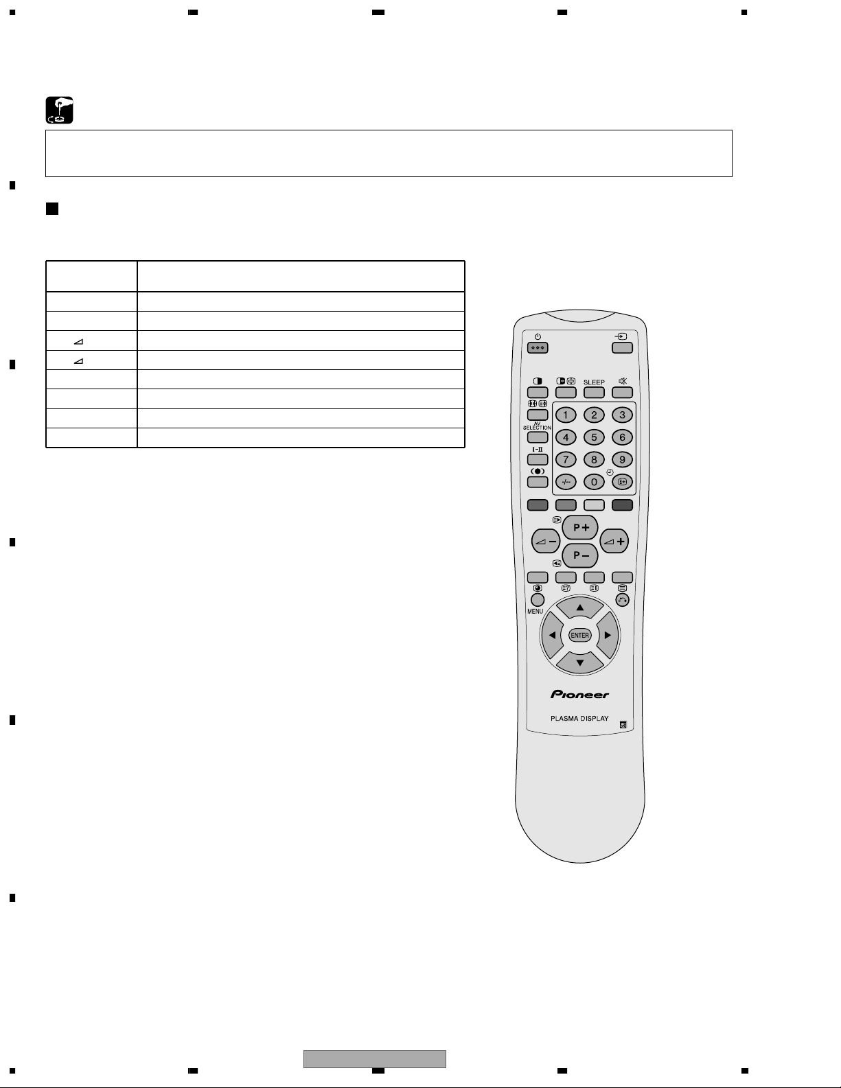
1234
6. ADJUSTMENT
6.1 SERVICE FACTORY MODE
A
Service factory mode uses an OSD function of the Media Receiver (PDP-R03E or PDP-R03U).
Perform the adjustment and setting in the state that this unit and Media Receiver are connected by the system.
Plasma display cannot use a factory mode by being simple.
Remote Control Unit Operation in The Service Factory Mode
Operate the service factory mode with the remote control unit (AXD1463 or AXD1460) of accessory of the media receiver.
Please perform the adjustment by operating the following keys.
B
C
D
Remote
Control Key
P + key
P – key
VOL + key
VOL – key
5 key
∞ key
2 key
3 key
Function
One line moves the selection cursor of the adjustment item up.
One line moves the selection cursor of the adjustment item down.
+1 raises a adjustment value
–1 reduces a adjustment value
Perform page down (previous page)
Perform page up (next page)
–10 reduces a adjustment value
+10 raises a adjustment value
E
F
56
1234
PDP-503PC
Page 57
5678
Perform the following operation by the remote control unit for less than 3 seconds.
• Press the "MENU" key
• Press the "ENTER" key
• Press the "0" key
Press the "Factory" key (Note 1)
Switch a page
with "5" and "∞" keys.
Press the "Factory" key (Note 1)
Press the " (POWER)" key (POWER OFF)
System standby state
Confirm that the plasma display and the media receiver turned on together and a
system cable is connected properly.
Image receiving state
Page 1/13
General information of the Plasma Display and Media Receiver
Service Factory Mode
Page 2/13 to 9/13
Adjustment and setting item of the Media Receiver
Page 11/13 to 13/13
Adjustment and setting item of the Plasma Display
Note 1: When use the adjustment exclusive use remote control unit with a [AA5F] code.
∗ : Be careful so that there is the case that page constitution is different.
6.1.1 How to Enter the Service Factory Mode
A
B
C
D
PDP-503PC
56
E
F
7
8
57
Page 58
1234
6.1.2 General Information of the Plasma Display and Media Receiver
Display example of the first page
A
1/13
CEN TE
RVers
1
2
OSD V e r s i o n
CV I C Ve r s i o n
3
4
TTXP Ve r s i on
5
MON I T OR V e r s i o n
6
PANE L V e r s i o n
7
FLASH Ve r s i on
8
MON I T OR Mo d e l
9
Mod e l S l eect inMa
Mod e l S l eectAV
10
11
Mod e l S l eect
12
B
Senso re Temp
Cen te r cuAtime
13
14
Mon i t or Ac u t i me 4 7 H 4 2 M
15
16
Pu l se Ac ut ime 164
17
18
ion
MON I T OR
MR M IAN 0021E
MR O DS2 0109A//010
W2 0 0 /109 0 009:12/X200/109 0 079:12/V20
TTX RPG
F6 91 10
-00
-05
01
0
4
0
28
+
OFF
RESET
RESET OFF
RESET OFF
NPIU S1GINoT
025H9//
H41M16
No. Item Explanation
C
D
E
1 Main software version information of the media receiver
2 OSD version information of the media receiver
IP/resize IC control software version information of the
3
media receiver
Text microcomputer software version information of the
4
media receiver
5
Module microcomputer software version information of the PDP
6 Panel microcomputer version information of the PDP
7 Panel flash ROM version information of the PDP
8 PDP model information
9 Media receiver model information
10 Media receiver model information
11 PDP destination information
Temperature information of panel temperature sensor on
12
the PDP
13 Media receiver accumulation operating time
14 Media receiver accumulation operating time reset
15 PDP accumulation operating time
16 PDP accumulation operating time reset
17 PDP accumulation pulse number
18 PDP accumulation pulse number reset
Reference
01: PIONEER 50 inches, 02: PIONEER 43 inches,
11: SHARP 50 inches, 12: SHARP 43 inches
0: All SHARP destinations, Japanese and North America destinations of
PIONEER, 3: European and general destinations of PIONEER
This is internal temperature information. This is not establishment
environment temperature.
Turn the display to [ON] by pressing the "VOL +" key, then it becomes [0H]
when pressing the "ENTER" key.
Turn the display to [ON] by pressing the "VOL +" key, then it becomes [0H]
when pressing the "ENTER" key.
Real accumulation pulse number becomes "indicated value *10,000,000 pulse".
Turn the display to [ON] by pressing the "VOL +" key, then it becomes [0]
when pressing the "ENTER" key.
0/109 0 109:12/
061
∗ : Be careful so that there is the case that page constitution is different.
F
58
1234
PDP-503PC
Page 59
5678
Display example of the eleventh page
1
2
3
4
5
6
7
8
9
10
11
12
13
14
15
16
17
18
MN T R
11/13 PUT1NoSIGNI
V50 0 2WB
MN T R V 6 0 0 1WB
MN T R PC 0 1WB
MN T R R H 2 5 5IGH1
MN T R R H 2 5 5IGH2
MN T R G H 2 5 5IGH2
MN T R B H 2 5 4IGH2
MN T R G H 2 5 5IGH1
MN T R B H 2 5 4IGH1
MN T R R L 5 1 0OW1
MN T R G L 5 0 9OW1
MN T R B L 5 1 2OW1
MN T R R L 5 1 0OW2
MN T R G L 5 1 1OW2
MN T R B L 5 1 2OW2
No. Item Adjustable Range Shipping Setting Storage Place
1
PDP_W/B table selection at VIDEO 50Hz
1 or 2
2
PDP
2
PDP_W/B table selection at VIDEO 60Hz
1 or 2
1
PDP
3
PDP_W/B table selection at PC
1 or 2
1
PDP
4
RED_GAIN of PDP_W/B table 1
0 to 255
Factory adjustment value
PDP
5
GREEN_GAIN of PDP_W/B table 1
0 to 255
Factory adjustment value
PDP
6
BLUE_GAIN of PDP_W/B table 1
0 to 255
Factory adjustment value
PDP
7
RED_OFS of PDP_W/B table 1
0 to 999
Factory adjustment value
PDP
8
GREEN_OFS of PDP_W/B table 1
0 to 999
Factory adjustment value
PDP
9
BLUE_OFS of PDP_W/B table 1
0 to 999
Factory adjustment value
PDP
10
RED_GAIN of PDP_W/B table 2
0 to 255
Factory adjustment value
PDP
11
GREEN_GAIN of PDP_W/B table 2
0 to 255
Factory adjustment value
PDP
12
BLUE_GAIN of PDP_W/B table 2
0 to 255
Factory adjustment value
PDP
13
RED_OFS of PDP_W/B table 2
0 to 999
Factory adjustment value
PDP
14
GREEN_OFS of PDP_W/B table 2
0 to 999
Factory adjustment value
PDP
15
BLUE_OFS of PDP_W/B table 2
0 to 999
Factory adjustment value
PDP
Caution in the PDP W/B (No.4 to 15) adjustment:
Adjustment value is reflected without relation in input signal during adjustment to the actual PDP.
For example, when operate a adjustment value of [MNTR HIGH1] during PAL input, switch to the adjustment value operation of W/B table 1
while displaying PAL in the actual PDP.
This is temporary.
After adjustment, it becomes the W/B table 2 operation in the PAL input after restarted in the normal mode. It becomes an operation of the
W/B table 1 adjustment value after adjustment in the NTSC input.
As for the above example, table selection (No. 1 and 2) becomes the shipping setting.
∗ : Be careful so that there is the case that page constitution is different.
6.1.3 Adjustment and Setting Item of the Plasma Display
A
B
C
D
E
56
PDP-503PC
F
7
8
59
Page 60
1234
Display example of the twelfth page
A
21/13 PUT1NoSIGNI
ABL V
1
2
3
4
5
6
7
8
IDE 11860 PCO
ABL V I DE 1 2 250O
VOF AD J 1 3 1S
VSU ADJ 1 2 8S
XSU ADJ 08SB
XSU ADJ 08SG
YSU ADJ 08SB
YSU ADJ 08SG
9
10
11
12
13
B
14
15
16
17
18
No. Item Adjustable Range Shipping Setting Storage Place
1 Electric power setting at the PC, VIDEO 60Hz 0 to 255
2 Electric power setting at VIDEO 50Hz 0 to 255
C
3 VOFS voltage setting 0 to 255
4 VSUS voltage setting 0 to 255
5 SUS_B timing setting of X drive 0 to 15
6 SUS_G timing setting of X drive 0 to 15
7 SUS_B timing setting of Y drive 0 to 15
8 SUS_G timing setting of Y drive 0 to 15
Factory adjustment value
Factory adjustment value
Factory adjustment value
Factory adjustment value
Factory adjustment value
Factory adjustment value
Factory adjustment value
Factory adjustment value
PDP
PDP
PDP
PDP
PDP
PDP
PDP
PDP
Adjustment item of this page is related in damage of the set when mistakes adjustment. When adjustment is needed, be enough
careful to adjustment.
D
Caution in the electric power setting (No. 1 and 2) adjustment:
Adjustment value is reflected without relation in input signal during adjustment to the actual PDP.
For example, when operate a adjustment value of [ABL VIDEO 60 PC] during PAL input, switch to the adjustment value operation of [ABL
VIDEO 60 PC] while displaying PAL in the actual PDP. This is temporary.
After adjustment, it becomes the [ABL VIDEO 50] operation in the PAL input after restarted in the normal mode. It becomes an operation of
the [ABL VIDEO 60PC] adjustment value after adjustment in the NTSC input.
∗ : Be careful so that there is the case that page constitution is different.
E
F
60
1234
PDP-503PC
Page 61

5678
Display example of the thirteenth page
1
2
3
4
5
6
7
8
9
10
11
12
13
14
15
16
17
18
VIPCDDEEO
NEGAT
21/13 PUT1NoSIGNI
DR 0 0VE MOI
DEDR VE MO
DEMO
I
VEI
PAT TE NR
ENHAN ECBR I GHT
FREQMAS K
FULL MASK
MA SK
V
03
OFF
OFF
OFF
OFF
50
No. Item Adjustable Range Shipping Setting Storage Place
1 Drive mode selection at VIDEO 0 to 5 0 PDP
2 Drive mode selection at PC 0 to 5 3 PDP
3 Negative positive inversion mode OFF/ON OFF PDP
4 Bright enhance OFF/ON OFF None
5 Refresh rate at mask signal generation 50/60/70 – None
6 Pattern mask signal generation OFF/ OFF PDP
7 Full mask signal generation OFF/ OFF PDP
Caution in the mask (generation test signal screen in the PDP inside) signal generation:
• A pattern mask and a full mask can use only either.
Therefore, turn a full mask to OFF when uses a pattern mask. Also turn a pattern mask to OFF when uses a full mask.
• A pattern mask and a full mask are test signal screens occurring together in the PDP inside. Therefore, in the mask signal generation, it
cannot confirm video inputting from OSD and the outside.
When release mask setting or change of each setting or perform the confirmation of the adjustment or external input signal, perform key
operation of the main unit button or the remote control unit.
When operated something, stop the generation of the mask signal just after that for two seconds. Therefore, modification and adjustment of
each setting and confirmation of the external input signal are possible.
∗ : Be careful so that there is the case that page constitution is different.
A
B
C
D
E
56
PDP-503PC
F
7
8
61
Page 62
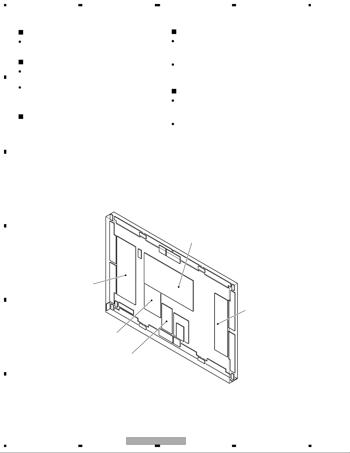
1234
6.2 ADJUSTMENT REQUIRED WHEN THE SET IS REPAIRED OR REPLACED
SW POWER SUPPLY Module
A
When replaced
No adjustment required.
DIGITAL VIDEO Assy
When repaired
No adjustment required.
Y DRIVE Assy
When repaired
1. VOFS/VH/IC5V voltage adjustment
2. Timing adjustment of pulse module
When replaced
1. SUSB ground timing adjustment
2. Panel white balance adjustment
When replaced
• Remove IC1204 (24LC04(1) SN-TBB) from the former PC
Board to replace, and install it to the new PC Board.
B
C
MR INTERFACE Assy
• Set slide SW according to page 22.
X DRIVE Assy
When repaired
1. VRN voltage adjustment
2. Timing adjustment of pulse module
When replaced
1. SUSB ground timing adjustment
2. Panel white balance adjustment
SW POWER SUPPLY
Module
D
Y DRIVE
Assy
X DRIVE
Assy
E
DIGITAL VIDEO
Assy
MR INTERFACE
Assy
Fig. 1 PC Board Location (rear side view)
F
62
1234
PDP-503PC
Page 63
5678
VOFS (Offset voltage) adjustment
Method 1
1. Write down a adjustment value of VOFS ADJ in the factory mode.
2. Set this adjustment value to center (128).
3. Adjust VR2701 so that the voltage between K2701 (VOFS) and K2703 (SUS GND)
becomes 45V.
4. Return it to the value that wrote down a adjustment value of V-OFFSET in step 1.
Method 2
1. Read the adjustment value of VOFS ADJ in the factory mode.
2. Adjust VR2701 so that the voltage between K2710 (VOFS) and K2703 (SUS GND)
becomes following voltage ± 0.5V.
VH (voltage for scan IC) Adjustment
Adjust so that the voltage between K2716 (VH) and K2720 (PSUS) becomes 103V ± 0.5V.
PSUS (=GNDH) is a floating GND and the electric potential is different from that of chassis
GND. Be sure not to short-circuit PSUS (=GNDH) and another GND, because that may
damage the unit.
The symptom is case of mis-adjustment
If the VH adjustment is not performed properly, dots like blinking luminance points appear. If
deviated greatly from the right adjustment point, panel will light white.
Input Signal
Adjusting Point
Adjusting Method
White 100%
VR2701 (VOFS)
(Y DRIVE Assy)
VR2703 (VH)
(Y DRIVE Assy)
IC5V Adjustment
Adjust so that the voltage between K2707 (IC5V) and K2720 (PSUS) becomes 5.0V ± 0.1V.
PSUS (=GNDH) is a floating GND and the electric potential is different from that of chassis
GND. Be sure not to short-circuit PSUS (=GNDH) and another GND, because that may
damage the unit.
The symptom is case of mis-adjustment
If the VOFS Voltage adjustment is not performed properly, dots like blinking luminance points
appear. If deviated greatly from the right adjustment point, panel will light white.
VR2702 (IC5V)
(Y DRIVE Assy)
Note : Be sure to measure between specified test points.
Input
Command
DAC
Output
Setting
Voltage
Input
Command
DAC
Output
Setting
Voltage
VOF000 0.4 25 VOF134 2.599212598 45.94488
VOF006 0.4984375 25.9375 VOF141 2.71496063 47.04724
VOF013 0.61328125 27.03125 VOF147 2.814173228 47.99213
VOF019 0.71171875 27.96875 VOF153 2.913385827 48.93701
VOF026 0.8265625 29.0625 VOF160 3.029133858 50.03937
VOF032 0.925 30 VOF166 3.128346457 50.98425
VOF038 1.0234375 30.9375 VOF172 3.227559055 51.92913
VOF045 1.13828125 32.03125 VOF179 3.343307087 53.0315
VOF051 1.23671875 32.96875 VOF185 3.442519685 53.97638
VOF058 1.3515625 34.0625 VOF191 3.541732283 54.92126
VOF064 1.45 35 VOF198 3.657480315 56.02362
VOF070 1.5484375 35.9375 VOF204 3.756692913 56.9685
VOF077 1.66328125 37.03125 VOF211 3.872440945 58.07087
VOF083 1.76171875 37.96875 VOF217 3.971653543 59.01575
VOF090 1.8765625 39.0625 VOF223 4.070866142 59.96063
VOF096 1.975 40 VOF230 4.186614173 61.06299
VOF102 2.0734375 40.9375 VOF236 4.285826772 62.00787
VOF109 2.18828125 42.03125 VOF242 4.38503937 62.95276
VOF115 2.28671875 42.96875 VOF249 4.500787402 64.05512
VOF122 2.4015625 44.0625 VOF255 4.6 65
VOF128 2.5 45
VOFS/VH/IC5V Voltage Adjustment
6.3 ADJUSTMENT
A
B
C
D
E
56
PDP-503PC
F
7
8
63
Page 64

A
1234
Sustain Pulse Waveform Adjustment
Input Signal
White 100%
Adjusting Point Adjusting Method
REF_DIG mode
in Factory mode
XSUSB ADJ
YSUSB ADJ
X-SUS-B, Y-SUS-B Adjustment
Set to the indicated value with the remote control unit.
(Refer to "Timing adjustment of control signal of X and Y Drive Assys".)
VRN Voltage Adjustment
Input Signal
Adjusting Point Adjusting Method
B
White 100%
VR3701 (VRN)
(X DRIVE Assy)
VRN (minus reset voltage adjustment)
Adjust so that the voltage between K3707 (VRN) and K3702 (SUS-GND) becomes
-300V ± 1.0V.
Panel White Balance Adjustment
Input Signal
C
∗ When perform the various adjustment by RS-232C control, execute a "DM0" command (release the limit of pulse number)
beforehand.
After the adjustment completion, execute a "DM 3" command (Limit of pulse number: 64%, shipping state) by all means.
D
Adjusting Point Adjusting Method
Adjust the parameter in the OFFSET-DIGITAL of factory mode as follows;
In this time, dispay uses the mask (MASK04) of factory mode.
PANEL R-HIGH
PANEL B-LOW
Reference : Adjustment values using the Media color-difference meter (A-100)
MASK Left Side
x 295
y 306
MASK Right Side
291
300
E
F
64
1234
PDP-503PC
Page 65
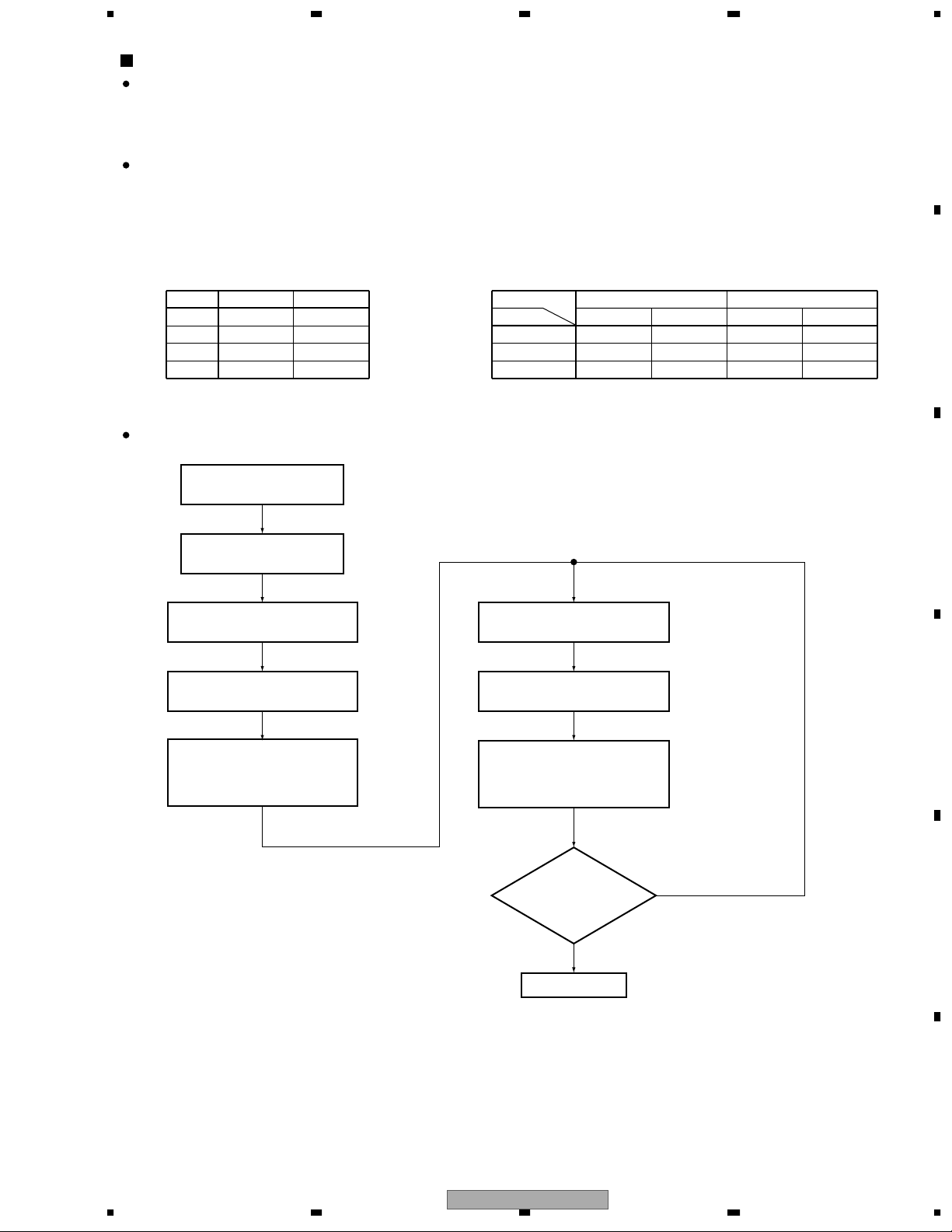
5678
Timing Adjustment of X and Y DRIVE Assys Control Signal
As for this adjustment, adjustment with set state is difficult.
Therefore replace it every Assy when replacing the pulse module.
Adjustment VR Test pin for adjustment and measurment
Display a SUSOUT waveform
Power ON and display a SUSOUT
waveform
Display a SUS-D waveform
Display a SUS-U waveform
Power ON and
display a SUS-D waveform
Display a SUS-U waveform
Measuring points of waveform
are refered to next page.
Power ON
Black Mask Screen
Coarse adjustment of
SUS-U, SUS-B, SUS-G
SUS-D adjustment
Adjust the waveform to 20-25ns.
SUS-U adjustment
Adjust the waveform to 20-25ns.
Power OFF
Compare waveform,
and do harmonize
almost?
Yes
No
Adjust VR resistance value
of SUS-B and SUS-G to match
VR resistance value of SUS-D
within ± 2Ω.
Adjust VR resistance value
of SUS-B and SUS-G to match
VR resistance value of SUS-D
within ± 2Ω.
Power OFF
Adjustment end
SUS-D readjustment
Adjust the waveform to 20-25ns.
SUS-U readjustment
Adjust the waveform to 20-25ns.
X DRIVE Y DRIVE
SUS-U VR3203 VR2204
SUS-D VR3202 VR2203
SUS-B VR3201 VR2202
SUS-G VR3200 VR2201
Pulse Module X DRIVE Y DRIVE
Upper Lower Upper Lower
SUSOUT K3105 K3106 K2212 K2203
SUS-U K3200 K3204 K2220 K2224
SUS-D K3108 K3205 K2207 K2225
Purpose
• Pulse module loads in DRIVE Assy as one of heat measures of DRIVE Assy. Adjust the drive timing of the pulse module
driving parallel with VR.
• Pulse module has each peculiar delay time. Readjustment is necessary when replaced the pulse module in the X and
Y DRIVE Assys.
Adjustment Method
CR delay circuit is each inserted on signal path of four control signals (SUS-U, SUS-B, SUS-D, SUS-G) driving
the pulse module.
Quantity of delay can adjust pulse module of one side with VR.
Adjust VR while measuring a waveform of the pulse module, and match a timing.
Adjustment Procedure
A
B
C
D
E
56
PDP-503PC
F
7
8
65
Page 66
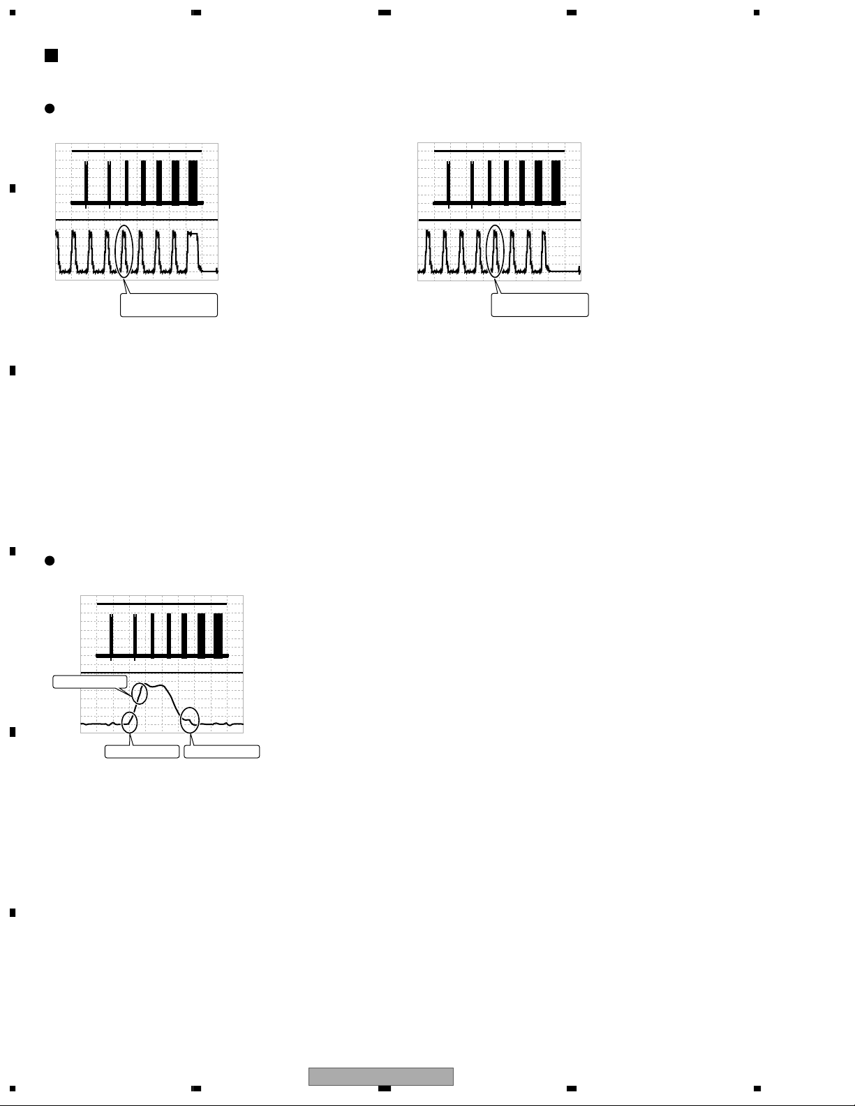
1234
Measuring Waveform of Pulse Module Timing Adjustment
Timing adjustment of the pulse module control signal adjusts with the sustain pulse of eighth pulse (X DRIVE) and
A
the ninth pulse (Y DRIVE) from the back of 6SF.
Measuring point of waveform
Y DRIVE SUSOUT waveform X DRIVE SUSOUT waveform
1SF 2SF 3SF 4SF 5SF 6SF 7SF
1ms/div
Magnify 6SF block
CH1 : Y SUSOUT Under (K2203), 50V/div
CH2 : Y SUSOUT Upper (K2212), 50V/div
CH4 : YPR-U1 (K2038)- Trigger, 5V/div
B
5µs/div
Use this sustain pulse
and adjust.
Trigger : 2msec delay
• Perform adjustment of waveform with a black mask screen.
• It is easy to adjust when turned field AB offset to OFF (RS-232C
command: OCN) in adjustment.
Note:
• Sampling rate of oscilloscope sets it more than 500MS/s in order
to perform ns order adjustment.
• Collecting calibration of probe before adjustment by all means.
• Connect a GND probe to the SUSGND terminal to measure the
C
waveform.
If this is not done there may be errors in adjustment.
1SF 2SF 3SF 4SF 5SF 6SF 7SF
1ms/div
Magnify 6SF block
CH1 : X SUSOUT Under (K3106), 50V/div
CH2 : X SUSOUT Upper (K3105), 50V/div
CH4 : YPR-U1 (K2038)- Trigger, 5V/div
5µs/div
Use this sustain pulse
and adjust.
Trigger : 2msec delay
When took waveform be each drive Assy unit, measure it at the
fourth sustain pulse from the back except for a large width sustain
pulse.
Therefore, when measured both waveform of the X and Y drives
together, it becomes the sustain pulse of 8 and 9 pulses from the
back.
Waveform coarse adjustment
Measure the SUSOUT waveform
When there is a gap with waveform of CH1 / CH2 of the part which
enclosed in the following circle, adjust required VR to overlap the
waveform.
D
1ms/div
Magnify the adjustment waveform
Adjust with SUS-B
CH1 : Y SUSOUT Under (K2203), 50V/div
CH2 : Y SUSOUT Upper (K2212), 50V/div
CH4 : YPR-U1 (K2038)- Trigger, 5V/div
500ns/div
Adjust with SUS-U Adjust with SUS-G
E
Trigger : 2msec delay
F
66
PDP-503PC
1234
Page 67

5678
CH1 : Y SUSOUT Under (K2203), 50V/div
CH2 : Y SUSOUT Upper (K2212), 50V/div
CH4 : YPR-U1 (K2038)- Trigger, 5V/div
Trigger : 2msec delay
CH1 : Y SUS-D Under (K2225), 50V/div
CH2 : Y SUS-D Upper (K2207), 50V/div
CH4 : YPR-U1 (K2038)- Trigger, 5V/div
Trigger : 2msec delay
CH1 : Y SUS-U Under (K2224), 50V/div
CH2 : Y SUS-U Upper (K2220), 50V/div
CH4 : YPR-U1 (K2038)- Trigger, 5V/div
Trigger : 2msec delay
SUS-D Adjustment (Y DRIVE)
Waveform Confirmation after Adjustment completion
Measurement of the SUSOUT waveform
SUS-U Adjustment (Y DRIVE)
1ms/div
5µs/div
1ms/div
5µs/div
1ms/div
500ns/div
1ms/div
10ns/div
1ms/div
500ns/div
• Check whether there is a large gap between the CH1 and CH2 waves
in the circled part of the 500 ns graph.
• In this specific case the drive power needs to be on, but whenever
possible turn the drive power off (RS-232C command: DRF).
If the drive power is on the pulse module temperature will increase
and the waveform will be harder to measure accurately.
20 - 25ns
1ms/div
200ns/div
Lower PM
Upper PM
Lower PM
Upper PM
1ms/div
10ns/div
20 - 25ns
Caution:
Not absolutely mistaking upper
and lower of waveform.
Magnify 6SF block
Magnify 6SF block
Magnify 6SF block
Magnify 6SF block
Magnify the adjustment waveform
Magnify 6SF block
Magnify 6SF block
Magnification Magnification
Magnification
Magnification
A
B
C
D
E
F
56
PDP-503PC
7
8
67
Page 68
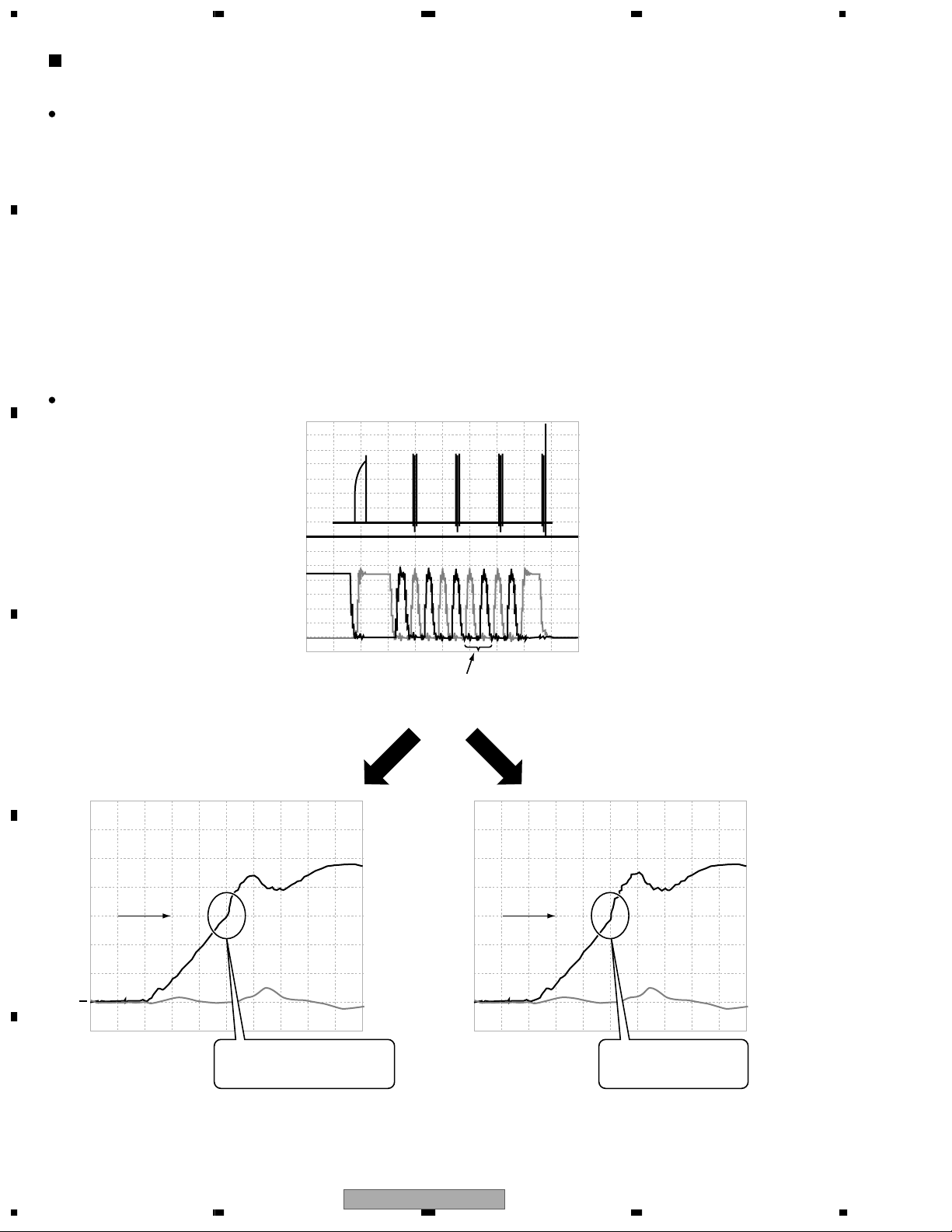
1234
SUS-B Ground Timing Adjustment
It is necessary to readjust this adjustment when replaced the X or Y DRIVE Assy and the pulse module.
A
B
Measurement point and method
Measurement point of waveform of X and Y DRIVE Assy in timing adjustment is test pin of SUSOUT of the pulse module of
bottom of the main unit.
X DRIVE Assy : K3106 Y DRIVE Assy : K2203
Measurement screen : White mask
The measurement is easy to perform when turns field AB alternation to OFF. (RS-232C command: OCN)
Measure a sustain pulse of the fourth pulse (X DRIVE) and the fifth pulse (Y DRIVE) from the back of the fourth FS, and
adjust. In the start section of this sustain pulse, waveform has inflection point with the timing when SUS-B becomes ON.
Adjust so that the voltage of this inflection point is the nearest to 150V and do not become less than 150V.
Adjustment parameter
X DRIVE: XSUSB (RS-232C command : XSB)
Y DRIVE: YSUSB (RS-232C command : YSB)
Note:
• Connect a GND probe to the SUSGND terminal to measure the waveform.
If this is not done there may be errors in adjustment.
Waveform in the measurement
Rst
C
1ms/div
Magnify 4SF block
XXXXXXY Y YYY Y
5µs/div
D
Magnify the fourth pulse sustain pulse (XSUSOUT waveform) from the back of the above waveform.
1SF 2SF 3SF 4SF
CH1 : Y SUSOUT (K2203), 50V/div
CH2 : X SUSOUT (K3106), 50V/div
CH4 : YPR-U1 (K2038)- Trigger, 5V/div
Trigger : 2msec delay
Measure a waveform of this section and adjust.
NG
OK
100msec/div
100msec/div
E
GND
F
68
150V Line
50V/div
This broken section moves by
changing the adjustment
parameter.
150V Line
50V/div
Become less than 150V.
→ NG
PDP-503PC
1234
Page 69

5678
VR2702
(IC5V_ADJ)
VR2201
(SUS_G_ADJ)
VR2202
(SUS_B_ADJ)
VR2203
(SUS_D_ADJ)
VR2204
(SUS_U_ADJ)
K2205
K2004
K2001
K2002
K2003
K2005
K2009
K2013
K2010
K2011
K2226
(SUS_U)
K2212
(SUSOUTB)
K2225
(SUS_D)
K2224
(SUS_U)
K2203
(SUSOUTA)
K2227
(SUS_D)
K2218
(1/2 VSUS)
K2214
(SUS_G)
K2215
(SUS_B)
K2217
(SUS_U)
K2716
(VH)
K2720
(PSUS)
K2717
(VH CONT)
K2216
(SUS_D)
VR2703
(VH_ADJ)
K2715
(YDC_DC_PD)
K2718
(VH UVP)
K2719
(VH OVP)
K2708
(VOFS)
K2705
(SUSGND)
K2702
(VSUS)
K2709
K2703
(SUSGND)
VR2701
K2222
K2211
K2710
(VOFS)
K2712
(VOFSUVP)
K2221
(+15V)
K2045
K2049
K2047
K2044
K2050
K2048
K2046
K2012
(PN MUTE)
K2038
(YPR_U1)
K2040
(YCP_MSK)
K2053
(SOFT_D)
K2041 (OFS)
K2039 (YSUS_MSK)
K2037 (YSUS_G)
K2028 (YSUS_U)
K2021
(YPR_U2)
K2029
(YSUS_D)
K2027
(YSUS_B)
K2024
(DGND)
K2101
(DEW_DET)
K2043
(DGND)
K2008
(DGND)
K2007
(DGND)
K2006
(+5V)
K2707
(IC5V)
K2714
(GNDHS)
K2704
(VF-)
K2701
(VF+)
K2706
(+14V)
K2711
(-8V)
K2713
(IC5V UVP)
VR3200
(SUS-G)
VR3201
(SUS-B)
VR3202
(SUS-D)
VR3203
(SUS-U)
K3103
(VCP_PD)
K3104
(+5V)
K3001
(+5V)
K3003
(XSUS-B)
K3015
(XSUS-MSK)
K3017
(XCP-MSK)
K3012
(XSUS-D)
K3014
(XNR-D1)
K3025
K3007
K3010
(XNR-U)
K3008
(PN_MUTE)
K3021
K3022
K3011
K3704
(VRN. CNT)
K3703
(SUS. GND)
K3701
(VSUS)
K3029
K3006
K3009
K3030
K3705
VRN UVP)
K3706
(X DC-DC PD)
K3708
(VRN_OVP)
VR3701
(VRN. ADJ)
K3707
(VRN)
K3702
(SUS. GND)
K3213
(1/2VSUS)
K3214
(SUSGND)
K3205
(SUS_D)
K3204
(SUS_U)
K3106
(SUSOUT_B)
K3102
(XNR_PD)
K3203
(1/2VSUS)
K3201
(SUSGND)
Adjusting Points
Y DRIVE Assy X DRIVE Assy
K3108
(SUS_D)
K3200
(SUS_U)
K3105
(SUSOUTA)
K3004 (XSUS-U)
K3013 (XSUS-G)
K3018 (XNR-D2)
A
B
C
D
E
PDP-503PC
56
F
7
8
69
Page 70
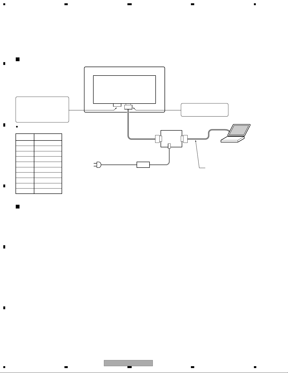
1234
6.4 COMMAND
6.4.1 RS-232C Command
As for PDP-503P system, the 232C control of the panel control item is possible by a single state.
A
However, the following exclusive use communication jig is necessary.
∗ Be careful so that can not use a DSUB 9-pin in the rear panel of the media receiver.
Connection
B
DVI (Video line):
Input optional video from the
signal source with the DVI
output.
Input timing is as follows.
DVI input timing
XGA60 (VESA conformity)
CLK 65MHz
H total 1344 clk
H disp 1024 clk
H sync 136 clk
C
H BP 160 clk
V total 806 line
V disp 768 line
V sync 6 line
V BP 29 line
fH 48.363 kHz
fV 60.004 Hz
PDP rear view
AC-DC adapter
(9V or 12V output)
Communication line:
Connect a system cable.
Exclusive use
communication jig
PC for control
Connect to DSUB 9-pin
DSUB 9-pin straight cable
Communication baudrate
D
E
F
38400 bps is fixed.
70
1234
PDP-503PC
Page 71

Jig Schematic Diagram
CN1
AKP1201
CN2
AKB1099
CN4
AKP1205
CN3
AKP1194
CN5
B3B-PH-SM3-TBB
R4
R
C1
1/50
IC1
DS14C232CM-TBB
IC2
PQ05DZ51-TLB
100R5100
R8
GND
9.3V
D1
D1FS4-TRB
D2
D1FS4-TRB
9V
NC
GND
G_JIGU10
100
1234567
8
16151413121110
9
C1+V+C1-
C2+
C2-V-DOUT2
RIN2
VCC
GND
DOUT1
RIN1
ROUT1
DIN1
DIN2
ROUT2
C3
1/50
C5
47/16
C7
47/16
C8
0.1
C4
0.1
C2
1/50
C6
R14
100k
1/50
L
G_JIGU10
R15
100k
R12
2.2k
R11
2.2k
R16
10k
R17
10k
R1
1k
R3
0
R2
0
C9
0.1
G_JIGU10
C10
47/16
VIN VO
VC
GND
NC
R6
100
R13
0
R7
100
V_JIGU10
R9
0
R10
SP_L
CSEN1
CSEN2
CCKM
GND
SMPOW
SP_R
SENCE
GND
RXD0_M
SP_L
GND
SRST
FLASH_W
GND
SR_UP
SR_DOWN
SP_R
GND
TXD0_M
0
201918171615141312
11
10
987654321
5678
A
B
C
D
E
PDP-503PC
56
7
F
71
8
Page 72
1234
RS-232C Command
dnammoCemaNnoitcnuF
A
B
C
D
E
0BAEDOMECNEREFERLBAeulavecnereferotLBAehtteS
1BA1EDOMTESFFOLBA1eulavtesffootLBAehtteS
2BA2EDOMTESFFOLBA2eulavtesffootLBAehtteS
3BA3EDOMTESFFOLBA3eulavtesffootLBAehtteS
LBATSUJDALBA timilreppurewopcirtcelefotnemtsujdA
NMAFFOETUMOIDUAemulovrekaepsfotseuqerffoetuM
YMANOETUMOIDUAemulovrekaepsfotseuqeretuM
FRDFFOEVIRDFFOevirD
NRDNOEVIRDNOevirD
0WD0NWOD01htiweulavtnemtsujdaehtnwoD
FWDLLUFNWODeulavtnemtsujdaehteziminiM
nWDnNWODnhtiweulavtnemtsujdaehtnwoD
NWEONETIRWMORPEE edomgnitirwMORPEEyalp&gulpehtetelpmoC
YWESEYETIRWMORPEE edomgnitirwMORPEEyalp&gulpehttratS
05FOEDIV05NUREERF ecneuqes)oediv(zH05htiwneercsksamehtyalpsiD
06FOEDIV06NUREERF ecneuqes)oediv(zH06htiwneercsksamehtyalpsiD
16FCP06NUREERF ecneuqes)CP(zH06htiwneercsksamehtyalpsiD
07FCP07NUREERF ecneuqes)CP(zH07htiwneercsksamehtyalpsiD
JAGTSUJDATEG yalpsidehtfoeulavtnemtsujdasuoiravehteriuqcA
WPGB/WLENAPTEG lenapehtfoeulavtnemtsujdaB/WehteriuqcA
1SG1SUTATSTEGnoitamrofninoisrevehteriuqcA
SMHTESRETEMRUOHemitlanoitpootretemruohteS
00M00KSAMFFOedomksaM
10M10KSAM)pmaL(1nrettaP
20M20KSAM)rabroloC(2nrettaP
30M30KSAM)enilgnitnalS(3nrettaP
40M40KSAM)tnemerusaemB/W(4nrettaP
50M50KSAM)tnemtsujdaB/W(5nrettaP
60M60KSAM)tnemerusaemkaepB/W(6nrettaP
70M70KSAM)tnemerusaemkaeP(7nrettaP
80M80KSAM)noitavreseR(8nrettaP
90M90KSAM)tsetnoitcetorpCINACS(9nrettaP
01M01KSAM)tsetnoitcetorpCINACS(01nrettaP
11M11KSAM)noitavreser(11nrettaP
21M21KSAM)noitavreser(21nrettaP
31M31KSAM)noitavreser(31nrettaP
41M41KSAM)noitavreser(41nrettaP
15M15KSAM)etihw(ksamlluF
25M25KSAM)472nayc(ksamlluF
35M35KSAM)3201atnegam(ksamlluF
45M45KSAM)rolochself(ksamlluF
55M55KSAM)3201nayc(ksamlluF
65M65KSAM)elprupthgil(ksamlluF
75M75KSAM)eulbyks(ksamlluF
85M85KSAM)der(ksamlluF
95M95KSAM)neerg(ksamlluF
06M06KSAM)eulb(ksamlluF
16M16KSAM)kcalb(ksamlluF
26M26KSAM)977der(ksamlluF
36M36KSAM)812nayc(ksamlluF
46M46KSAM)444nayc(ksamlluF
56M56KSAM)34rolochself(ksamlluF
66M66KSAM)026der(ksamlluF
76M76KSAM)89atnegam(ksamlluF
86M86KSAM)34_1eulbyks(ksamlluF
96M96KSAM)34_2eulbyks(ksamlluF
07M07KSAM)34elprupthgil(ksamlluF
tceriD
ytidilaV
ΟΟ
NWOD/PU
ytidilaV
rewoL
timiL
000552
reppU
timiL
F
72
PDP-503PC
1234
Page 73
5678
RS-232C Command
dnammoCemaNnoitcnuF
tceriD
ytidilaV
NWOD/PU
ytidilaV
rewoL
timiL
reppU
timiL
17M17KSAM)wolley(ksamlluF
27M27KSAM)619eulb(ksamlluF
37M37KSAM)noitavreser(ksamlluF
47M47KSAM)noitavreser(ksamlluF
NMMONEDOMRORRIM)yalpsidlamron(FFOedomrorriM
XMMXEDOMRORRIMyalpsidgnisrevertfeldnathgiR
YMMYEDOMRORRIMyalpsidgnisrevermottobdnapoT
ZMMYXEDOMRORRIM yalpsidgnisrevertfeldnathgirmottobdnapoT
NTMONETUMLENAPetumlenapesaeleR
YTMSEYETUMLENAPetumlenaP
NMNONEDOMEVITAGENFFOedomnoisrevnievitisopevitageN
YMNSEYEDOMEVITAGENNOedomnoisrevnievitisopevitageN
HBPHGIHEULBLENAPtnemtsujdaTHGILHGIHEULB
ΟΟ
000552
LBPWOLEULBLENAPtnemtsujdaTHGILWOLEULB
ΟΟ
000999
HGPHGIHNEERGLENAPtnemtsujdaTHGILHGIHNEERG
ΟΟ
000552
LGPWOLNEERGLENAPtnemtsujdaTHGILWOLNEERG
ΟΟ
000999
NHPONTHGIL-THGIHLENAP lenapehtfoedommumixamthgilhgihB/WehtesaeleR
YHPSEYTHGIL-THGIHLENAP mumixamotlenapehtfothgilhgihB/WehtteS
NLPONECNAHNETHGIRB FFOecnahnenoitcerrocssenthgirbretneC
YLPSEYECNAHNETHGIRB NOecnahnenoitcerrocssenthgirbretneC
SMPTESRETEMESLUPretemeslupehtfognitteslanoitpO
FOPFFOREWOPtseuqerybdnatS
NOPNOREWOPtseuqerNOrewoP
HRPHGIHDERLENAPtnemtsujdaTHGILHGIHDER
ΟΟ
000552
LRPWOLDERLENAPtnemtsujdaTHGILWOLDER
ΟΟ
000999
NCPONEDOMCP noitcelesecneuqesOEDIV:tupnizH06ehttA
YCPSEYEDOMCP noitcelesecneuqesCP:tupnizH06ehttA
0TP0PMETROLOCLENAP )FER(0otedomerutarepmethcaeteS
1TP1PMETROLOCLENAP )1SFO(1otedomerutarepmethcaeteS
2TP2PMETROLOCLENAP )2SFO(2otedomerutarepmethcaeteS
0PU0PUeulavtnemtsujdaehtezimixaM
FPULLUFPUeulavtnemtsujdaehtezimixaM
nPUnPUnhtiweulavtnemtsujdaehtesiR
FOVTSUJDATESFFOVtnemtsujdasfoV
ΟΟ
000552
LOVEMULOVemuloV
ΟΟ
000060
USVTSUJDASUSVtnemtsujdasusV
ΟΟ
000552
BSXBSUSXtnemtsujdaeslupB-SUS-X
ΟΟ
000510
GSXGSUSXtnemtsujdaeslupG-SUS-X
ΟΟ
000510
BSYBSUSYtnemtsujdaeslupB-SUS-Y
ΟΟ
000510
GSYGSUSYtnemtsujdaeslupG-SUS-Y
ΟΟ
000510
A
B
C
D
56
PDP-503PC
E
F
7
8
73
Page 74

1234
6.4.2 GET Command
Command Description
A
Command Function
GAJ Output data of an electronic VR adjustment value and a drive system adjustment value
GPW Output data to be related to white balance adjustment of the panel
GS1 Output data such as version information, hour meter and pulse meter
GAJ: Output data of an electron VR adjustment value and a drive system adjustment value
• Output it according to transmission order and size of the table below.
Order Data Contents Size Remarks
B
C
1 Setting mode of electric power upper limit value 3 byte AB* ( *: 0 to 3)
2
Electric power upper limit value
3 (Offset data) 3 byte (Note 1)
(ABL)
4 Vsus adjustment value (Reference data) 3 byte
5 Vofs adjustment value (Reference data) 3 byte
6 V-SUS-B adjustment value (Reference data) 3 byte
7 V-SUS-G adjustment value (Reference data) 3 byte
8 Y-SUS-B adjustment value (Reference data) 3 byte
9 Y-SUS-G adjustment value (Reference data) 3 byte
(Note 1) : When performed in reference mode selection, offset data outputs the same value as the reference data.
(Note 2) : Checksum of 2 bytes is added at the end, but ignore it.
(Reference data) 3 byte
GPW (Get Panel White balance): Output data to be related to white balance adjustment of panel
• Output it according to transmission order and size of the table below.
Order Data Contents Size Remarks
1 Panel color temperature mode 3 byte PT* ( *: 0 to 3)
2
Gain of W/B adjustment value
3 (Offset data) 3 byte (Note 1)
Red
4
Gain of W/B adjustment value
5 (Offset data) 3 byte (Note 1)
Green
D
E
6
Gain of W/B adjustment value
7 (Offset data) 3 byte (Note 1)
Blue
8
Offset of W/B adjustment value
9 (Offset data) 3 byte (Note 1)
Red
10
Offset of W/B adjustment value
11 (Offset data) 3 byte (Note 1)
Green
12
Offset of W/B adjustment value
13 (Offset data) 3 byte (Note 1)
Blue
(Note 1) : When performed in reference mode selection, offset data outputs the same value as the reference data.
(Note 2) : Checksum of 2 bytes is added at the end, but ignore it.
(Reference data) 3 byte
(Reference data) 3 byte
(Reference data) 3 byte
(Reference data) 3 byte
(Reference data) 3 byte
(Reference data) 3 byte
F
74
1234
PDP-503PC
Page 75
5678
GS1: Output data such as version information, hour meter and pulse meter
• Output it according to transmission order and size of the table below.
Order Data Contents Size Remarks
1 Display information 3 byte See below
2 Module microcomputer model number 4 byte 5691 or F691
3 Module microcomputer version 3 byte
4 Panel microcomputer version 3 byte
5 Panel /FLASH ROM version 3 byte
6 Hour meter (hour) 5 byte Unit: H (time)
7 Pulse meter 7 byte Unit: 0.01G (10,000,000)
8 Main microcomputer model number 4 byte 5692 or F692
9 Main microcomputer version 3 byte
10 Wide microcomputer version 3 byte
11 Wide /FLASH ROM version 3 byte
Data Model
MX5 PDP-503MX (initial value)
MX4 PDP-433MX
MD5 Module 50 inches
MD4 Module 43 inches
HD5 PDP-503HD
HD4 PDP-433HD
Display Information
(Note) : Checksum of 2 bytes is added at the end, but ignore it.
A
B
C
D
E
56
PDP-503PC
F
7
8
75
Page 76
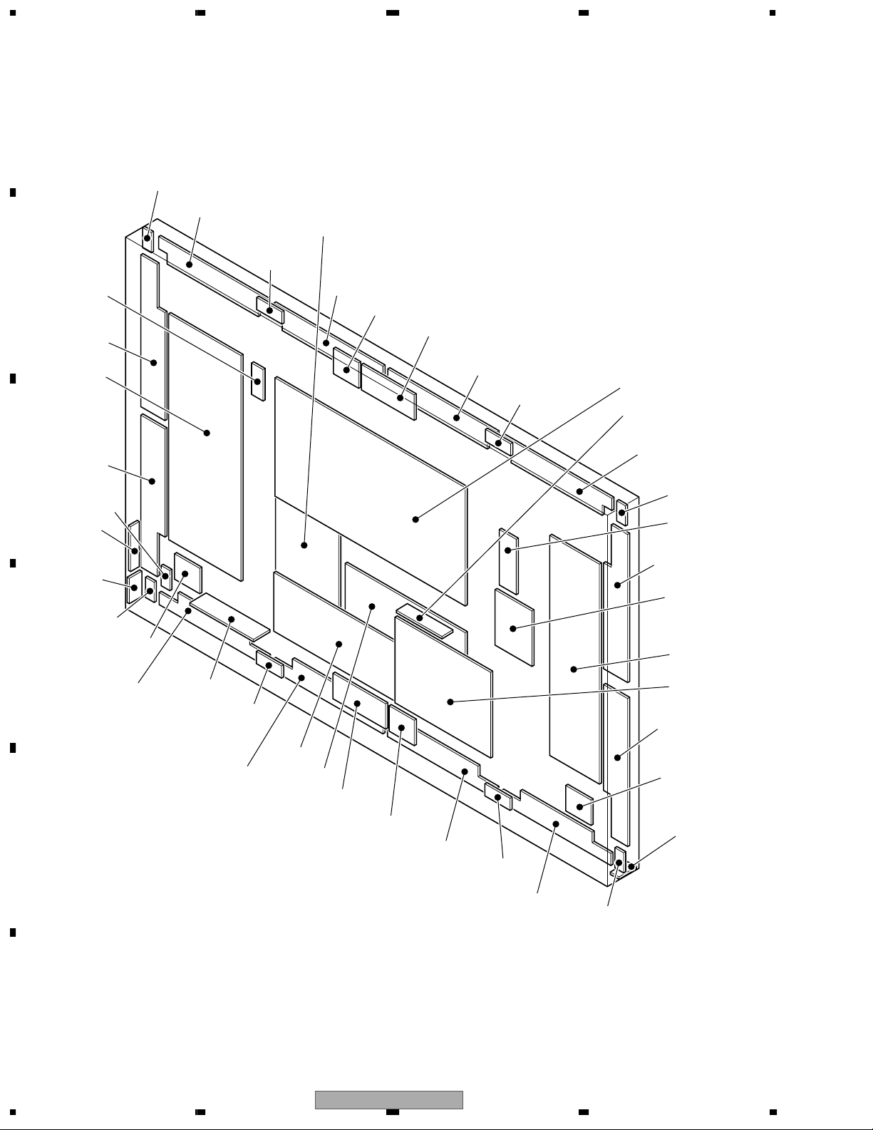
1234
7. GENERAL INFORMATION
7.1 DIAGNOSIS
7.1.1 PCB LOCATION
A
CLAMP A
Assy
ADR CONNECT A
Assy
BRIDGE A
Assy
B
THERMAL
SENSOR
Assy
SCAN (A)
Assy
Y DRIVE
Assy
DIGITAL VIDEO
Assy
ADR CONNECT B
Assy
SUB ADDRESS A
Assy
RESONANCE
Assy
ADR CONNECT C
Assy
BRIDGE B
Assy
SW POWER SUPPLY
Module
SLOT CONNECTOR
Assy
C
D
E
SCAN (B)
Assy
IR Assy
SIDE KEY
Assy
KEY
CONNECTOR
Assy
CLAMP C
Assy
SP OUT R
Assy
ADR CONNECT D
Assy
CONTROL
Assy
BRIDGE C
Assy
ADR CONNECT C
Assy
I/O Assy
RGB Assy
RESONANCE
Assy
SUB ADDRESS B
Assy
ADR CONNECT B
Assy
BRIDGE D
Assy
ADR CONNECT A
Assy
ADR CONNECT D
Assy
CLAMP B
Assy
V MID CLAMP
Assy
X CONNECTOR (A)
Assy
MX AUDIO
Assy
X DRIVE
Assy
Video Card
(PDA-5002)
X CONNECTOR (B)
Assy
SP OUT L
Assy
MX LED
Assy
CLAMP D
Assy
F
76
1234
PDP-503PC
Page 77
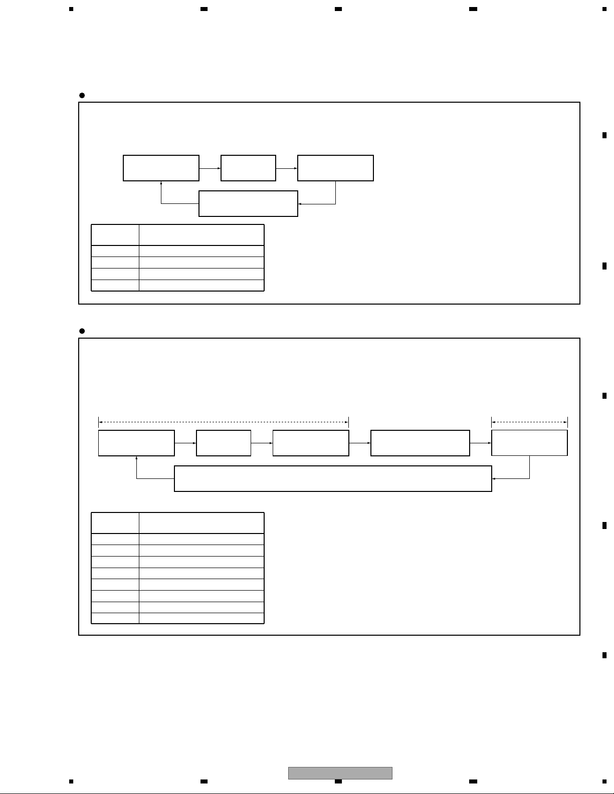
5678
• Operations : When a microcomputer detected abnormality, turn the power supply to OFF.
• LED display : Green blinks
How to release the shut down state
When turn the power supply ON by remote control units, release from the
shut down state, and turn the power supply ON.
(It is not necessary to turn the AC power OFF.)
How to release the power down state
AC power OFF
↓
Wait for PD LED in the power supply module disappearing
(for around 30 seconds).
↓
Afterwards, wait moreover for five seconds.
↓
Return by AC power ON.
* After power down release, this unit rises up in the standby state.
Examples: LED blinks in the DIGITAL-IIC communication NG
• Operations : When this unit becomes the dangerous state, turn the power supply OFF with the protection circuit.
• LED display : Red blinks
* When protection circuit more than two places almost worked simultaneously, display LED in order to 1st - 2nd.
Examples: LED blinks in the 1st power down = Y-DC/DC CONVERTER, 2nd power down = Y-DRIVE
Number of
blinks
Name
1 Panel Microcomputer NG
2 DIGITAL-IIC communication NG
3 Dewdrop abnormality
4 Temperature abnormality
Number of
blinks
Name
1 Y-DRIVE
2 Y-DC/DC CONVERTER
3 X-DC/DC CONVERTER
4 X-DRIVE
5 Power supply
6 Address junction
7 Address resonance
8 DIGITAL-DC/DC CONVERTER
Shut Down
Power Down
Green LED lights
for 200 msec.
Lights out
for 3 sec
Green LED lights
for 200 msec.
Lights out
for 100 msec
When internal circuit abnormality and other operation abnormality occurred from this unit, self-diagnose display function by STANDBY/ON
(LED) indicator is loaded.
Each NG point by LED blinking and a PD (power down) point are as follows.
1st power-down information
2nd power-down
information
Red LED lights
for 200 msec.
Lights out
for 3 sec
Lights out
for 1 sec
Red LED lights
for 200 msec.
Lights out
for 100 msec
Red LED lights
for 200 msec.
7.1.2 SHUT DOWN/POWER DOWN DIAGNOSIS BY LED DISPLAY
A
B
C
D
56
PDP-503PC
7
E
F
77
8
Page 78
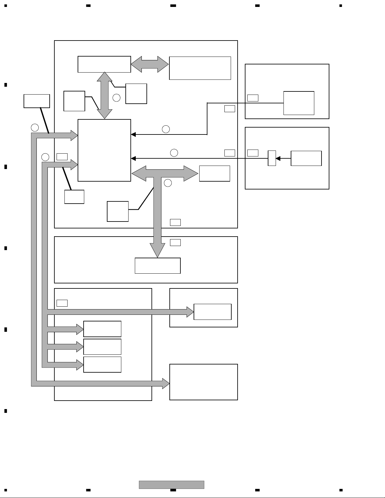
1234
A
DDC_SCL
DDC_SDA
B
2
DIGITAL VIDEO ASSY
IC1101
Panel UCOM
RXD
BUSY
REQ_PU
IC1207
D3
2
Module UCOM
IC1191
Panel UCOM
external Flash ROM
TXD
CLK
1
*PU_CE
D18
TEMP1
DEW_DET
4
3
IC1204
EEPROM
D6 Y2
THERMAL SENSOR
ASSY
TE1
IC8351
Thermal
Sensor 1
Y DRIVE ASSY
Moisture
Sensor
CN2002
2
A_SCL
A_SDA
C
SCL
SDA
D1
SW POWER SUPPLY
P2
MODULE
Expander
D
MR INTERFACE ASSY AUDIO ASSY
R3
CXA2021S
IC4204
SiI861
IC4005
Expander
IC4011
E
Expander
MEDIA
RECEIVER
Note: 1 - 4 show LED flashing number of times when shut down occurred in this route.
IC5202
F
78
1234
PDP-503PC
Page 79
5678
When a module microcomputer failed in communication with a panel
microcomputer, this NG occurs.
Shut down after OSD display for 30 seconds from the NG detection.
Abnormality to expect
Open / Short of communication line in the Assy
1 Panel microcomputer NG
When a module microcomputer failed in communication with outside
EEPROM or EXPANDER, this NG occurs.
Shut down after OSD display for 30 seconds from the NG detection.
* However, this communication NG may occur in the standby state.
Abnormality to expect
• Open / Short of communication line in the DIGITAL VIDEO, MR INTERFACE
and AUDIO Assys
• Breaking of wire of the following points is thought about.
DIGITAL VIDEO Assy (D1) ↔ SW POWER SUPPLY Module (P2)
DIGITAL VIDEO Assy (D3) ↔ MR INTERFACE Assy (R3)
MR INTERFACE Assy (R23) ↔ AUDIO Assy (A24)
System Cable
2 DIGITAL-IIC communication NG
When it becomes the dew drop state in this unit, this NG occurs.
After the dew drop detection, shut down immediately.
Abnormality to expect for dew drop
Disconnect a connector CN2002 between Dew drop sensor and Y DRIVE Assy.
3 Dew drop detection
When temperature of this unit became abnormally high, this NG occurs.
Shut down after OSD display from the NG detection for 30 seconds.
Note: When temperature fell down during indication, return to the normal operation.
Abnormality to expect when it occurs in the environment that is not
high-temperature
• Disconnect a connector between DIGITAL VIDEO Assy (D18) and
temperature sensor 1 (TE1).
Shut down temperature of each temperature sensor
Sensor Temp 78
4 Temperature abnormality
Reference
Shut down diagnosis
1
2
3
4
5
6
7
8
9
10
11
12
13
14
15
16
17
18
CEN TE
1/13
RVers
OSD V e r s i o n
CV I C V e r s i o n
TTXP Ve rs i on
ion
MON I T OR V e r s i o n
Mod e l S l eect inMa
Mod e l S l eectAV
Mod e l S l eect
Cen te r cuAtime
MON I T OR
RESET
RESET OFF
RESET OFF
OFF
+
0
0
4
28
F6 91 10
TTX RPG
W2 0 0 /109 0 009:12/X200/109 0 079:12/V20
061
0/109 0 109:12/
MR O DS2 0109A//010
MR M IAN 0021E
-05
-00
PANE L V e r s i o n
FLASH Ve r s ion
MON I TOR M o d e l
Mon i t or Ac u t i me 4 7 H 4 2 M
H41M16
01
Pu l se Acu t ime 1 64
Sensor e Temp
025H9//
NPIU S1GINoT
E06
E06
E04
A
B
C
D
56
PDP-503PC
7
E
F
79
8
Page 80

1234
A
Relay
Circuit
OR
X1
3
B
P4
4
X Drive X DC-DC
5
2
P3
1
X DRIVE ASSY
SW POWER
SUPPLY
MODULE
C
8
DC-DC
DIGITAL
P2
D1
OR
6
PD Circuit
7
Y1
Y Drive Y DC-DC
Y DRIVE ASSY
PD_TRIGGER
AND
D1202 Cathode DIG_ADR.PD
D
Mute
Address PD
OR
IC1201-pin 8
E
DIGITAL VIDEO ASSY
D11
-
D8
OR
ADR CONNECT
ASSY
(Upper)
D15
-
D12
ADR CONNECT
ASSY
(Lower)
OR
IC1201-pin 6
D16
RESONANCE
ASSY
(Upper)
OR
RESONANCE
ASSY
D17
(Lower)
Note: 1 - 8 show LED flashing number of times when power down occurred in this route.
F
80
1234
PDP-503PC
Page 81
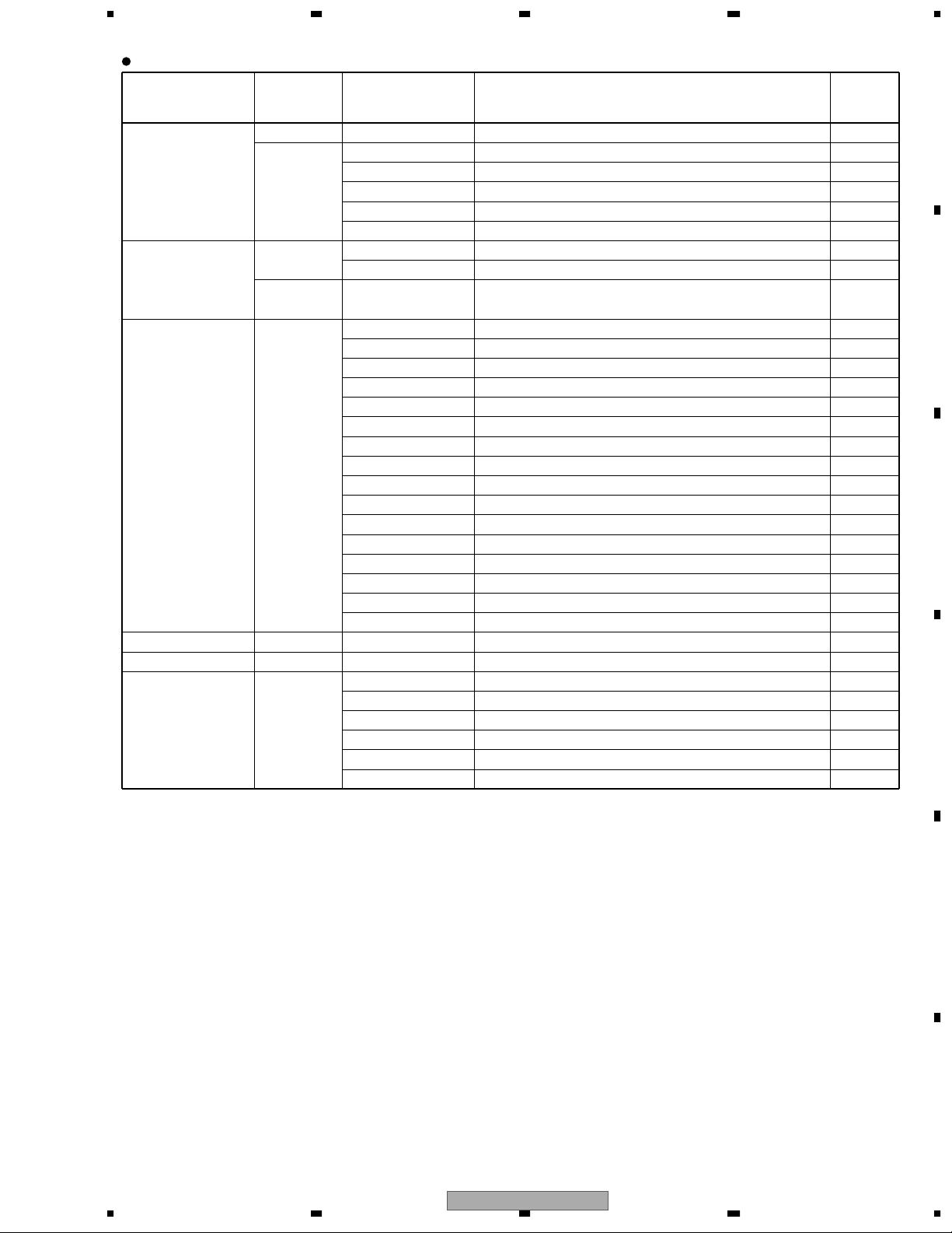
5678
Kind and function of the various protection circuit (P.D. circuit)
Reference
OVP : Over Voltage Protect
UVP : Under Voltage Protect
OCP : Over Current Protect
Note 1: AC200V P.D. is not applicable to the PDP-503PE and PDP-503PU models.
Assy Name
Red LED
Number of
Blinks
Kind of P.D.
Circuit
Function
Remarks
Y DRIVE Assy
1 VCP OCP P.D. by VCP overcurrent
2
VOFS OVP P.D. by VOFS overvoltage
VOFS UVP P.D. by VOFS undervoltage (= overcurrent)
VH OVP P.D. by VH overvoltage
VH UVP P.D. by VH undervoltage (= overcurrent)
IC5V UVP P.D. by IC5V undervoltage (= overcurrent)
X DRIVE Assy
3
VRN OVP P.D. by VRN overvoltage
VRN UVP P.D. by VRN undervoltage (= overcurrent)
4
VCP OCP P.D. by VCP overcurrent
SW POWER SUPPLY
Module
5
VSUS OVP P.D. by VSUS overvoltage
VSUS UVP P.D. by VSUS undervoltage (= overcurrent)
VADR OVP P.D. by VADR overvoltage
VADR UVP P.D. by VADR undervoltage (= overcurrent)
15V OVP P.D. by 15V overvoltage
15V UVP P.D. by 15V undervoltage (= overcurrent)
12V UVP P.D. by 12V undervoltage (= overcurrent)
6.5V OVP P.D. by 6.5V overvoltage
6.5V UVP P.D. by 6.5V undervoltage (= overcurrent)
13.5V UVP P.D. by 13.5V undervoltage (= overcurrent)
-9V UVP P.D. by -9V undervoltage (= overcurrent)
+B OVP P.D. by +B overvoltage
+B OCP P.D. by +B overcurrent
AC200V P.D. P.D. by AC200V apply Note 1
PFC module overheat protection
VSUS arc resistance overheat protection
ADR CONNECT Assy 6 ADR.PD P.D. by disconnecting the connector
RESONANCE Assy 7 ADR.K.PD P.D. by ICP open and TCP defective
DIGITAL VIDEO Assy 8
5.0V OVP P.D. by 5V overvoltage
5.0V UVP P.D. by 5V undervoltage (= overcurrent)
3.3V OVP P.D. by 3.3V overvoltage
3.3V UVP P.D. by 3.3V undervoltage (= overcurrent)
2.5V OVP P.D. by 2.5V overvoltage
2.5V UVP P.D. by 2.5V undervoltage (= overcurrent)
A
B
C
D
PDP-503PC
56
E
F
7
8
81
Page 82
1234
A
Diagnosis Condition
Note: About PS PD
The condition that Red LED blinks five times
(power supply PD)
B
Operation
P.D. Circuit
K2211 Lo VCP OCP
Drive section (control signal, output elements etc.) in
normal operation
K2709 Lo VOFS UVP
Drive section (control signal, output elements etc.) in
normal operation
IC5V D/D CONV. BLOCK in normal operation
K2718 Lo VH UVP
K2713 Lo IC5V UVP
Drive section (control signal, output elements etc.) in
normal operation
K3705 Lo VRN UVP
K3103 Lo VCP OCP
When P4 connector disconnected, P.D. does not occur
When P3 connector disconnected, P.D. does not occur
When P6 connector disconnected, P.D. does not occur
When pin 5 of P2 connector disconnected, P.D. does
not occur
connectors disconnected
ADR. PD
1 When the internal protection circuit of SW
ADR. K. PD
↓
POWER SUPPLY Module worked
identify the PD point
2 When a microcomputer was not able to
Being careful because the protection circuit
of SW POWER SUPPLY Module cannot
conclude that worked.
5.0V OVP
K1901 Lo
K1902 Lo 5.0V UVP
K1903 Lo 3.3V OVP
K1904 Lo 3.3V UVP
K1905 Lo 2.5V OVP
K1906 Lo 2.5V UVP
C
D
IC2701, IC2702, IC2709, IC2715
IC2206, IC2214 (Pulse module), IC2203, IC2204,
IC2212, IC2213, IC2213, IC2217, R2209
Q2211, Q2212, R2277, IC2208, IC2210 VOFS D/D CONV. BLOCK in normal operation
SCAN IC
IC3200, IC3201 (pulse module), IC3103, IC3104,
IC3106, IC3107, IC3110, IC3113, R3109
Disconnect D8 - D15 connectors
TCP damage of IC6704 (ICP), disconnect D16 and
D17 connectors, panel microcomputer is defective,
outside Flash ROM of the panel microcomputer is
defective.
Error Pont Possible Part of Error Circuit State
E
VOFS D/D CONV. BLOCK (Y DRIVE Assy) IC2702, IC2709, IC2715 K2712 Lo VOFS OVP
VOFS D/D CONV. BLOCK (Y DRIVE Assy)
VH D/D CONV. BLOCK (Y DRIVE Assy) IC2712, IC2716 K2719 Lo VH OVP
VH D/D CONV. BLOCK (Y DRIVE Assy) IC2711, IC2712, IC2716
SCAN (A), (B) Assy SCAN IC VH D/D CONV. BLOCK in normal operation
IC5V D/D CONV. BLOCK (Y DRIVE Assy) IC2704, IC2706, IC2717 SCAN Assy in normal operation
Y DRIVE Assy
Operation
P.D. Point in
1 Y DRIVE
of
Diagnosis of the error point in the various protection circuit (P.D. circuit) operation (Red LED blinks)
Blinks
Number
2 Y DC DC
SCAN (A), (B) Assy
IC5V D/D CONV. BLOCK (Y DRIVE Assy) IC2704, IC2706, IC2717 SCAN Assy in normal operation
VRN D/D CONV. BLOCK (X DRIVE Assy) IC3702, IC3712 K3708 Lo VRN OVP
VRN D/D CONV. BLOCK (X DRIVE Assy) IC3701, IC3702, IC3712
X DRIVE Assy Q3122 VRN D/D CONV. BLOCK in normal operation
3 X DC DC
X DRIVE Assy IC3200, IC3201 (Pulse module)
4 X DRIVE X DRIVE Assy
Y DRIVE Assy IC2206, IC2214 (Pulse module)
MX AUDIO Assy IC8601 (Audio IC)
5
SW POWER SUPPLY Module SW POWER SUPPLY Module When the voltage is not output even if P4, P3 and P6
ADDRESS CONNECT A - D Assy,
RESONANCE Assy,
D/D CONV. BLOCK (DIGITAL VIDEO Assy)
PS
D/D CONV. BLOCK (DIGITAL VIDEO Assy) IC1901
D/D CONV. BLOCK (DIGITAL VIDEO Assy) IC1901
DC DC
6 ADR ADDRESS CONNECT A~D Assy
7 ADR K RESONANCE Assy
8 DIGITAL
D/D CONV. BLOCK (DIGITAL VIDEO Assy) IC1901
F
82
1234
PDP-503PC
Page 83
5678
AC IN
100 - 240V
Power Factor
Control
VSUS DC/DC
Converter
VOFS DC/DC
Converter
VADR DC/DC
Converter
6.5V DC/DC
Converter
(6.5V, 13.5V, -9V)
15V DC/DC
Converter
(15V, 12V)
ST-BY
Power Supply
STB5V
+B395V VSUS
13.5V
12V
-9V
VOFS
-45V
VH DC/DC
Converter
VH
130V
IC5V, VF12V
DC/DC
Converter
IC5V
VF12V
VADR
61V
VRN DC/DC
Converter
VRN
-300V
225V
SW POWER SUPPLY MODULE Y DRIVE ASSY
X DRIVE ASSY
15V DC/DC
Converter
(5V, 3.3V, 2.5V)
3.3V
2.5V
5.0V
DIGITAL VIDEO ASSY
Block diagram for Power supply section
Supplementary information
1. Power on/off switch for the large-signal system (SW102)
Function: Only the power for the small-signal system
(15V, 12V, 6.5V, 13.5V, and -9V) is on, and the
power for the large-signal system (VSUS, VADR) is
off.
Usage: Use when only an operational check for the small-
signal system is required.
Supplementary information:
When this switch is to be used, the wires of pin 5
(DIG, ADR, and PD) of the P2 connector of the
power-supply module should be disconnected to
prevent the PD circuit from operating. To turn the
power of the large-signal system off without using this
switch, operation from an external PC through
RS-232C commands "DRF" is basically required. In
this case, the above procedure is not required, as the
PD circuit is muted by software.
3. Temperature compensation of the VOFS voltage for
the drive system
Function: Control the power supply voltage mentioned above
according to temperature. (Temperature compensation
works so that the voltage is lowered on the lowertemperature side, and is raised on the highertemperature side.)
Purpose: To improve the yield by compensating the temperature
characteristics of the panel.
Supplementary information:
For this model, temperature compensation is performed only for the VOFS voltage, and not for the VSUS
voltage, and it is controlled by software.
4. When a fuse blows
• If a fuse blows, never turn the power on again only after
replacing the fuse. (In most cases, the fuse itself did not have
any problem. So as long as factors of overcurrent have not been
removed, chances of destruction increase every time the power
is turned on. In the worst case, about a dozen parts may be
destroyed.)
• Principally, the whole power-supply module must be replaced.
5. Voltage adjustment of the panel drive
As this model employs the electronic VR system for the VSUS
and VOFS voltages, and as the voltage-adjustment data are stored
in the DIGITAL assembly, voltage adjustment of the panel drive
is not necessary when the power-supply modules are changed.
(For VADR, VH, and VRN, adjustments with semifixed VR
controls are necessary.)
For this model, as the power-supply block has been developed
and designed by an outside vendor, at the point you know which
module is a cause of failure (through diagnosis described
elsewhere in this manual), change the corresponding modules, and
do not diagnose or repair the module.
Similarly, the switches and the semifixed VRs inside the powersupply module must not be adjusted without a special reason.
2. 200V AC power-down switch (SW101)
Function: While 200V AC voltage is applied, operation of the
PD circuit is turned on and off (ON when the switch is
set to 100V AC, and OFF when the switch is set to
200V AC).
Setting: For the PU model only, the switch is set to 100V,
and for other models, it is set to 200V.
Method of power supply ON in the large signal
system OFF state with RS-232C command
1 Confirm that this unit is the standby state.
2 Transmit RS-232C command "DRF."
3 Turn the power supply ON by remote control unit, side key
or command "PON."
∗ When turn the power supply OFF once, return to setting of
large signal system ON.
When turn the power supply ON in the large signal system
OFF, transmit "DRF" command each time.
A
B
C
D
E
F
56
PDP-503PC
7
8
83
Page 84
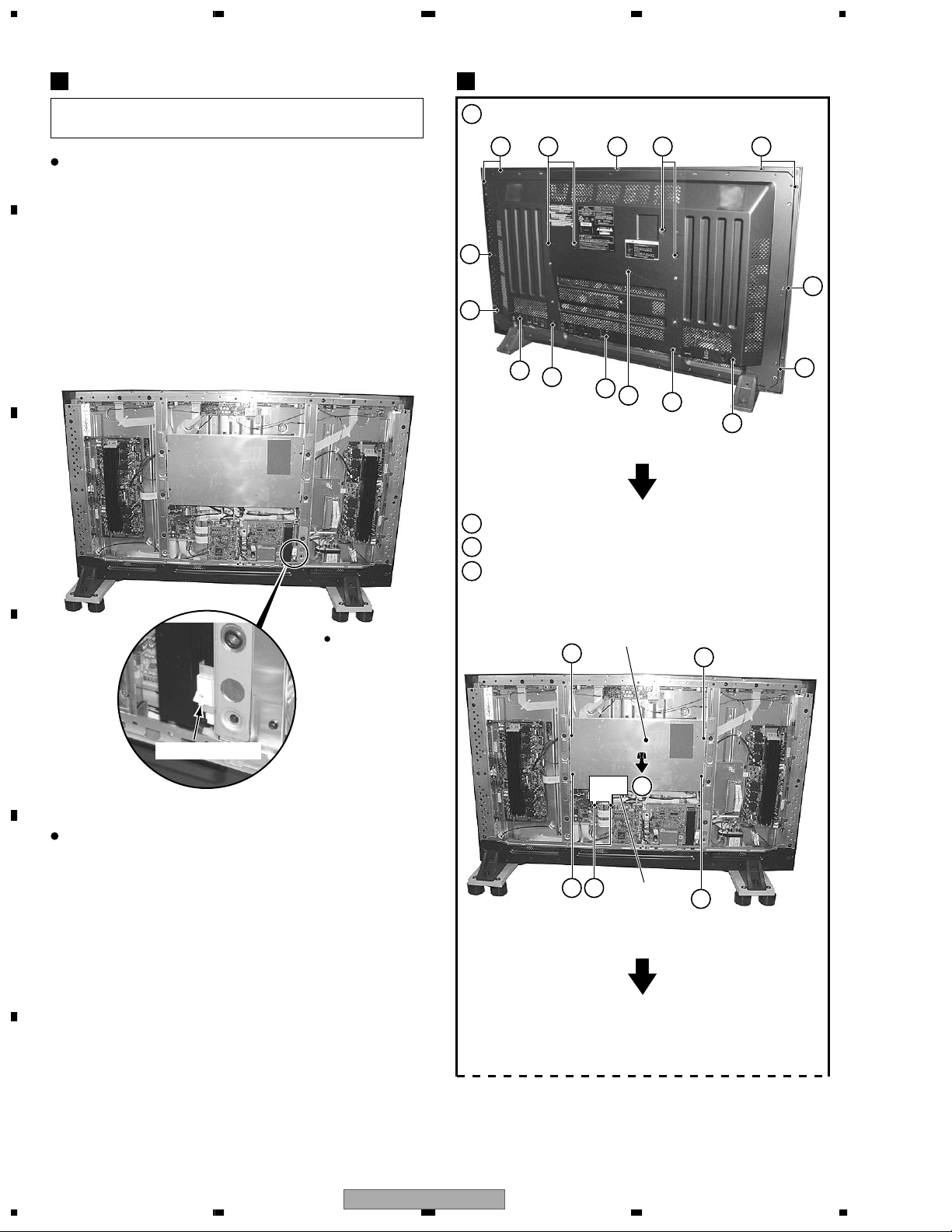
1234
7.1.3 DISASSEMBLY
A
This unit adopt the "Rear Case opened ! detection" system.
Please work in service as follows by all means.
Outline and caution
Perform video transmission from the media receiver to the
plasma display with digital signal in the PDP-503HD series.
Therefore adopt contents protection by HDCP for copyright
protection.
Moreover establish the detect switch which is never turned
on the power when "a rear case of plasma display was
opened carelessly".
Detect switch does not detect at the power supply OFF and
the remote control unit wait state. Please stick this detect
B
switch with tape before turning on the power in inside
diagnoses of the plasma display. And please remove it not
to forget the tape which stuck after the repair.
SW Power Supply ModuleAbout detect switch
Remove the Rear Case (50P).(Screws × 19)
1
×2
1
×2
1
1 1
1
1
1
1
1
1
1
1
×2 ×2
1
1
1
C
Rear View
D
Detect Switch (S2)
When detect switch has worked by any chance
When detect switch works, LED of red blinks in succession
by a 300msec period.
Press keys in order of "MENU" key, "ENTER" key and
"POWER" key with the remote control unit after sticking the
detect switch with tape or close the rear case beforehand.
E
This unit activates and it becomes the service factory mode
screen. Afterwards, turn off the power with the remote
control unit.
Perform the normal operation afterward.
Remove the IF Earth Metal.(Screws × 2)
2
Remove four screws.
3
Remove the SW Power Supply Module.
4
SW Power Supply
Module
3
4
×2
3
2
IF Earth
Metal
3
3
F
84
1234
PDP-503PC
Page 85
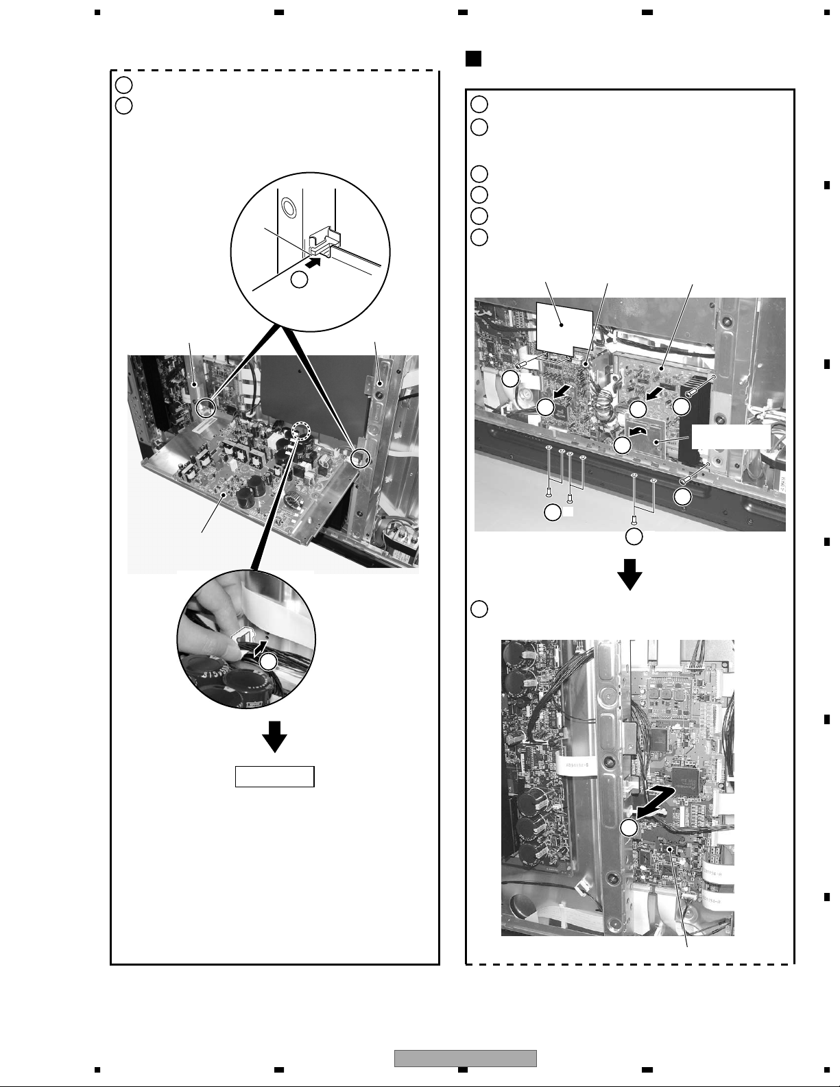
5678
1
Remove the Rear Case (50P). (Screws × 19)
3
Remove the IF Earth Metal (Screws × 2)
3
4
5
×2
5
×2
4
Remove the MR INTERFACE Assy (Connector, Screws × 4)
5
Remove the SP TERMINAL Assy (Connector, Screws × 2)
6
Remove the AUDIO AMP Assy (Connector, Screws × 2)
7
Remove the DIGITAL VIDEO Assy
(Connector,Circuit Board Spacer × 6)
2
Remove the SW Power Supply Module.
(Connector, Screws × 4)
MR INTERFACE, AUDIO AMP SP TERMINAL
and DIGITAL VIDEO Assys
MR INTERFACE
Assy
SP TERMINAL
Assy
IF Earth
Metal
AUDIO AMP Assy
DIGITAL VIDEO Assy
6
6
6
5
Insert it and reduce the Clamper.
Clamper
Sub Frame L
Slit
SW Power Supply
Module
Sub Frame R
6
Insert the SW Power Supply Module into the slit
of Sub Frame L and R.
6
SW Power Supply
Module
4
×4
7
Diagnosis
5
A
B
C
D
56
PDP-503PC
E
F
7
8
85
Page 86

1234
Y DRIVE, SCAN (A), (B) Assy
A
B
C
Remove the three screws.
1
Front Case 50 (P)
Loosen a rivet.
2
Remove the Lead Cover (P).
3
Pull out a Flexible Cable.
4
2
Lead Cover (P)
Rivet
Turn it not to press the rivet.
(Because when the rivet presses,
fit in once again.)
It is easy to remove when pull out
the Lead Cover (P) with the rivet
before completely removing the rivet.
×3
1
44
3
Lead Cover (P)
Remove the Rear Case (50P). (Screws × 19)
7
Remove the Y DRIVE Assy. (Connector, Screws × 8)
8
Remove the Front Chassis V. (Screws × 5)
9
9
9
8
8
×2
Y DRIVE Assy
×2
9
×2
8
×2
8
8
Reverse the SCAN (A) and SCAN (B) Assemblies.
Remove bottom by the fulcrum at the top of Front Case 50 (P).
5
Remove the Front Case 50 (P).
6
D
Front Case 50 (P)
Rear Case
10
When it is necessary, exchange the ROM.
11
SCAN (A) Assy
ROM
×6
6
Aluminum
Materials
It is the structure that a hook of
E
Front Case 50 (P) was put between
with Rear Case and aluminum materials.
5
10
10
SCAN (B) Assy
F
86
1234
PDP-503PC
Page 87
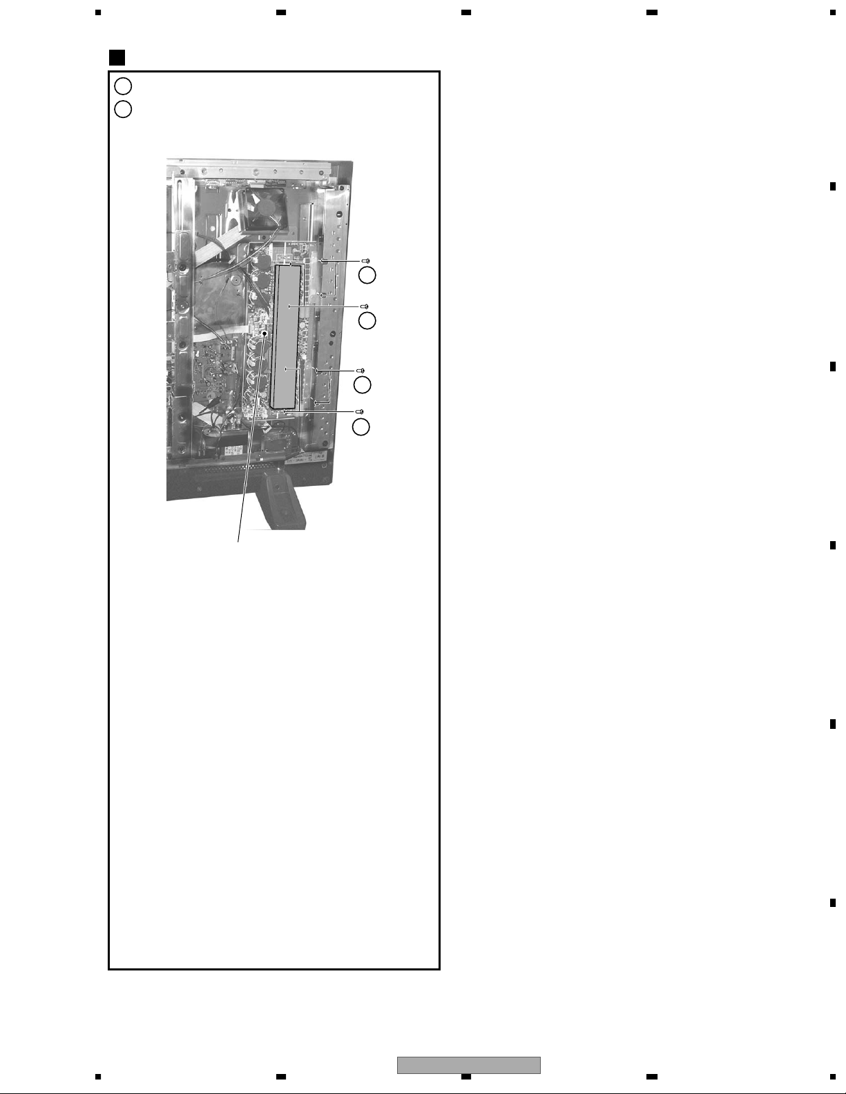
5678
1
Remove the Rear Case (50P). (Screws × 19)
2
Remove the X DRIVE Assy. (Connector, Screws × 8)
X DRIVE Assy
×2
2
×2
2
×2
2
×2
2
X DRIVE Assy
A
B
C
D
E
56
PDP-503PC
F
7
8
87
Page 88
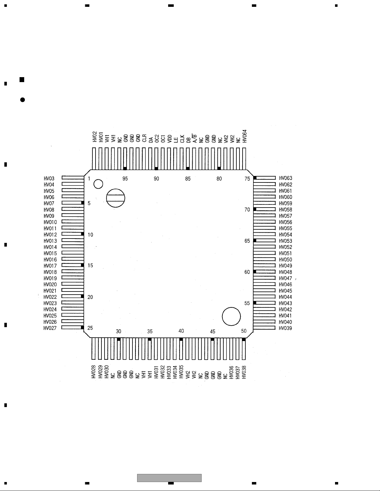
1234
7.2 IC INFORMATION
• The information shown in the list is basic information and may not correspond exactly to that shown in the schematic diagrams.
A
• List of IC
SN755864APZP, HD64F2328VF, PE1013B, M30624FGAFP, PD6358A, PST9246N, FS781BZB, STK795-460
SN755864APZP (SCAN A ASSY : IC6201 - IC6206, SCAN B ASSY : IC6001 - IC6006)
Scan IC
Pin Assignment (Top view)
B
C
D
E
F
88
1234
PDP-503PC
Page 89
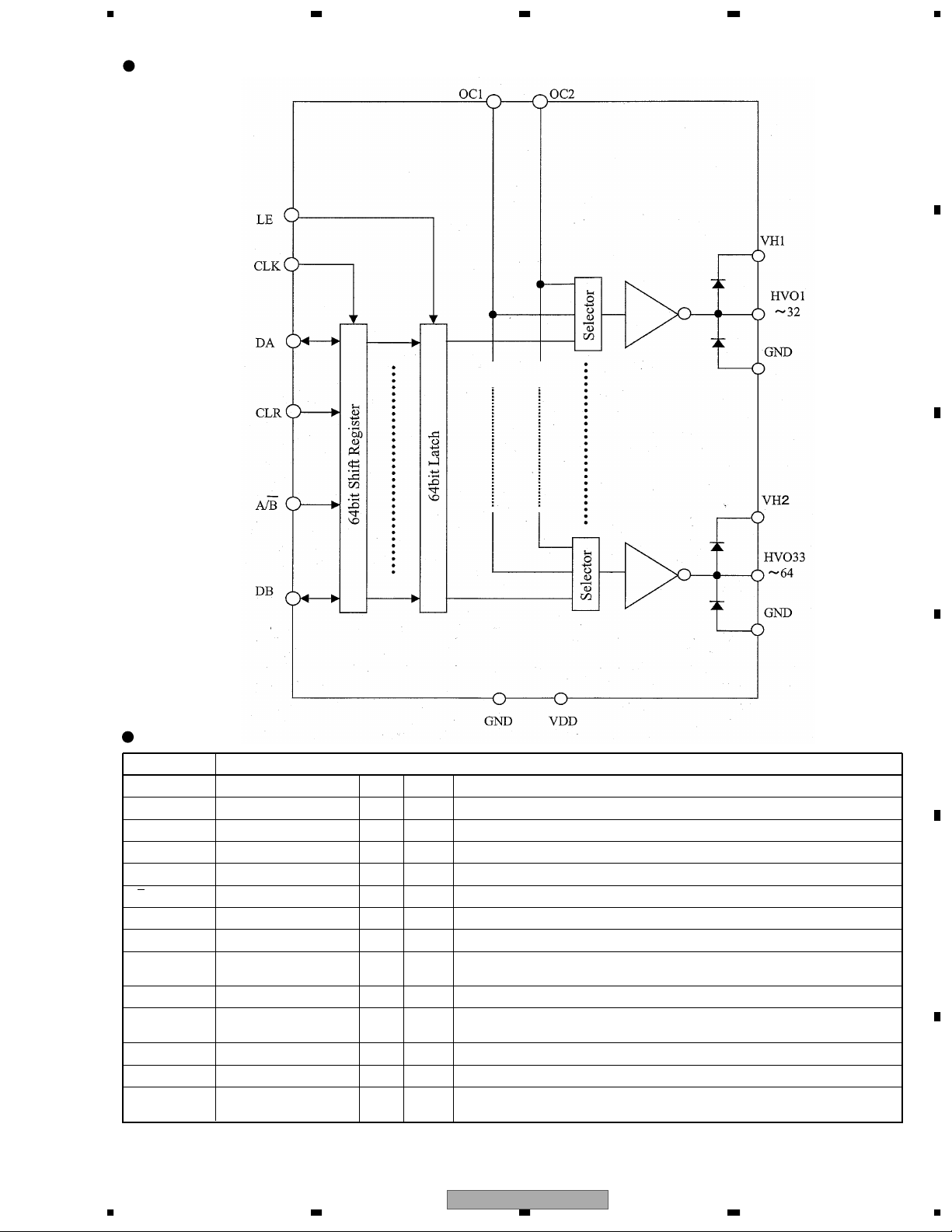
Pin Function
Block Diagram
Name Pin No. I/O Num. Function
CLK 86 I 1 Shift clock (start edge partial response)
DA 91 I/O 1 The serial data input of shifting register
DB 85 I/O 1 The serial data output of shifting register
LE 40 I 1 It output data done a latch of by "H" level
A/B 84 I 1 A shift directional control signal of shift register
CLR 92 I 1 It do data of shift register with "H" by "L" level
OC1 89 I 1 An output control terminal of HVO
OC2 90 I 1 An output control terminal of HVO
HVO
99, 100, 1-28
36-40, 48-76
O 64 High voltage drive output (HVO1 - HVO64)
VDD 88 − 1 Logic power supply
GND
30-32, 44-46
81-82, 93, 94-95
− 11 Standard potential. This is common to HVO1 - HVO64.
VH1 34, 35, 97, 98 − 4 The high potential circuit power supply which is common to HVO1 - HVO32
VH2 41, 42, 78, 79 − 4 The high potential circuit power supply which is common to HVO33 - HVO64
NC
29, 33, 43, 47
77, 80, 83, 96
− 8 It is the insulation electrically
5678
A
B
56
PDP-503PC
7
C
D
E
F
89
8
Page 90

1234
HD64F2328VF (DIGITAL VIDEO ASSY : IC1101)
Scan IC
A
B
C
D
E
F
Pin Function (1/3)
No. Pin Name Function
1 CS_23
2 NC NC Terminal
3 VSS GND
4 VSS GND
5 VCC 3.3V power supply
6 UA0 Address bus
7 UA1 Address bus
8 UA2 Address bus
9 UA3 Address bus
10 VSS GND
11 UA4 Address bus
12 UA5 Address bus
13 UA6 Address bus
14 UA7 Address bus
15 UA8 Address bus
16 UA9 Address bus
17 UA10 Address bus
18 UA11 Address bus
19 VSS GND
20 UA12 Address bus
21 UA13 Address bus
22 UA14 Address bus
23 UA15 Address bus
24 UA16 Address bus
25 UA17 Address bus
26 UA18 Address bus
27 UA19 Address bus
28 VSS GND
29 UA20 Address bus
30 PA5 NC terminal
31 PA6 NC terminal
32 PA7 NC terminal
33 CE_PN Enables / for panel microcomputer
34 CE_PN Enables / for panel microcomputer
35 VSS GND
36 VSS GND
37 APLP The APL value acquisition trigger signal input
38 VD_31 The V signal input from IC1401 (PD6358)
39 VCC 3.3V power supply
40 UD0 Data bus
41 UD1 Data bus
42 UD2 Data bus
43 UD3 Data bus
44 VSS GND
45 UD4 Data bus
46 UD5 Data bus
47 UD6 Data bus
48 UD7 Data bus
49 UD8 Data bus
50 UD9 Data bus
PE5064 (IC1703) control output
90
1234
PDP-503PC
Page 91

5678
Pin Function (2/3)
No. Pin Name Function
51 UD10
Data bus
52 UD11 Data bus
53 VSS GND
54 UD12 Data bus
55 UD13 Data bus
56 UD14 Data bus
57 UD15 Data bus
58 VCC 3.3V power supply
59 D_TXD Communication with IC1207 (module microcomputer)
60 EXT_TXD Communication with the outside (program notes)
61 D_RXD Communication with IC1207 (module microcomputer)
62 EXT_RXD Communication with the outside (program notes)
63 D_CLK Communication with IC1207 (module microcomputer)
64 P60 NC terminal
65 VSS GND
66 CS_FLASH A flash memory control terminal
67 VSS GND
68 VSS GND
69 P61 NC terminal
70 UDREQ IC1703 (PE5064) control terminal
71 P63 NC terminal
72 WE_FLASH A flash memory note control signal (unused)
73 BUSY The command receipt of a message lye Norwich output
74 REQ_PU A communication demand to a module microcomputer
75 SEL23B IC1703 (PE5064) control terminal
76 CLRB IC1703 (PE5064) control terminal
77 FR_SEL The free run select signal output
78 RST31B The reset output to IC1301, IC1401 (PD6358)
79 RST23B The reset output to IC1703 (PE5064)
80 FWE Microcomputer program note control signal
81 RESET Reset input
82 NMI The at the rate of tang input (unused)
83 STBY The hardware standby input (unused)
84 VCC 3.3V power supply
85 XTAL A clock oscillation child connection terminal
86 EXTAL A clock oscillation child connection terminal
87 VSS GND
88 PF7 NC terminal
89 VCC 3.3V power supply
90 PF6 NC terminal
91 RDB A read control terminal from an outside slave device
92 HWRB A wright control terminal to an outside slave device
93 PF3 NC terminal
94 PF2 NC terminal
95 PF1 NC terminal
NC terminal
96 PF0
NC terminal
97 P50
NC terminal
98 P51
GND
99 VSS
GND
100 VSS
56
PDP-503PC
A
B
C
D
E
F
7
8
91
Page 92
1234
Pin Function (3/3)
A
B
C
No. Pin Name Function
101 P52 NC terminal
102 P53 NC terminal
103 AVCC 3.3V power supply
104 VREF A/D, D/A reference voltage input (unused)
105 STOPB The drive control input from IC1703 (PE5064)
106 P41 NC terminal
107 RYBY The flash memory note ready input
108 ADR_K_EMG_L1 The emergency input from panel bottom address resonance block
109 ADR_K_EMG_U1 The emergency input from panel upper address resonance block
110 ADR_K_EMG_L2 The emergency input from panel bottom address resonance block (unused)
111 ADR_K_EMG_U2 The emergency input from panel upper address resonance block (unused)
112 P47 NC terminal
113 AVSS GND
114 VSS GND
115 MUTE_ADR The panel mute signal input
116 MUTE_SUS The X and Y drive mute signal output (unused)
117 P15 NC terminal
118 HD The HD signal input from outside Assy (RGB Assy etc.)
119 P13 NC terminal
120 P12 NC terminal
121 PC_VIDEO The PC/Video identification output
122 VD The HD signal input from outside Assy (RGB Assy etc.)
123 MD0 The microcomputer mode of operation select signal input
124 MD1 The microcomputer mode of operation select signal input
125 MD2 The microcomputer mode of operation select signal input
126 PG0 NC terminal
127 CS_31Y IC1301, IC1401 (PD6358) control signal
128 CS_31X IC1301, IC1401 (PD6358) control signal
D
E
F
92
1234
PDP-503PC
Page 93
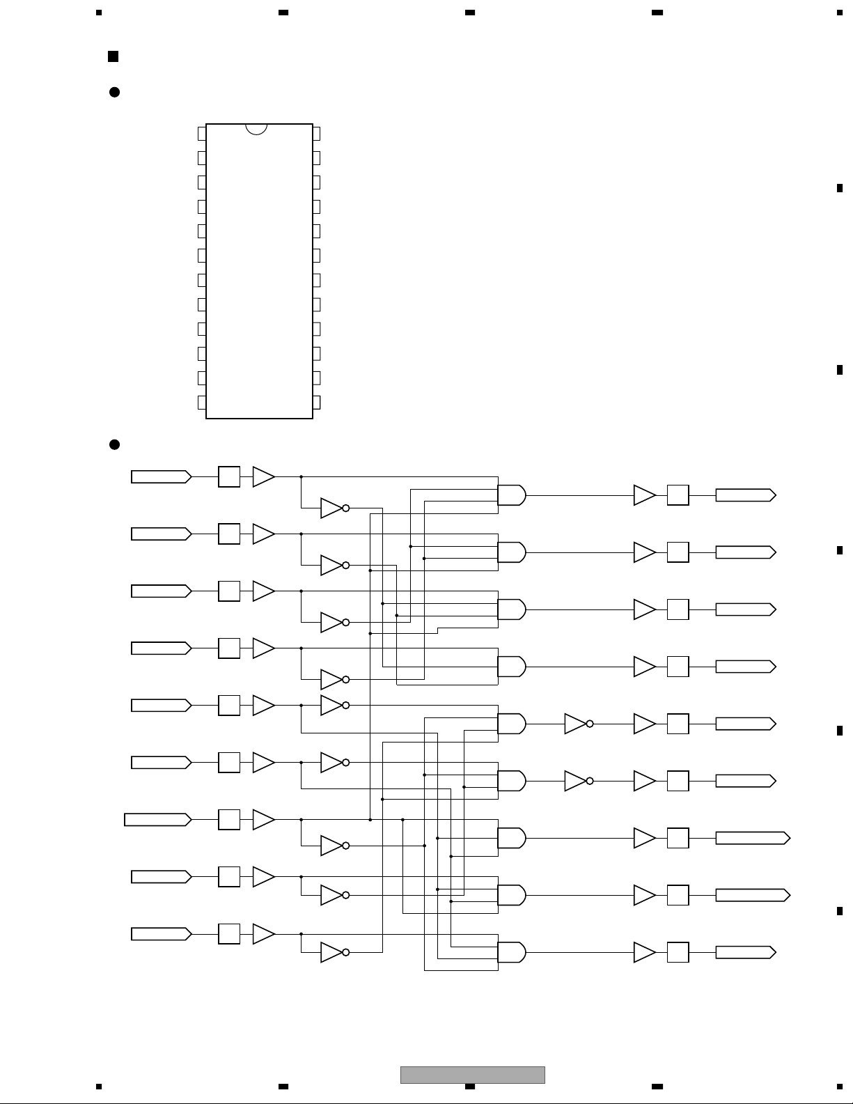
5678
Pin Assignment (Top View)
Block Diagram
PE1012A (X DRIVEASSY : IC3003)
Drive Protect PLD
124I/CLK
I
I
I
I
I
I
I
I
I
I
GND
XSUS_BI
VCC
I/O/Q
I/O/Q
I/O/Q
I/O/Q
I/O/Q
I/O/Q
I/O/Q
I/O/Q
I/O/Q
I/O/Q
I12 13
2
XSUS_BO
1_50
1_6
1_24 1_40
23
XSUS_UI
3
XSUS_UO
1_49
1_4
1_23 1_39
22
XSUS_DI
4
XSUS_DO
1_48
1_5
1_22 1_40
21
XSUS_GI
6
YSUS_GO
1_45
1_1
1_55 1_54
19
XNR_D1I
7
XNR_D1O
1_44
1_51
1_62 1_36
18
XNR_D2I
10
XNR_D2O
1_43
1_2
1_61 1_35
15
XSUS_MSKI
8
XSUS_MSKO
1_46
1_32
1_28 1_41
17
XCP_MSKI
9
XCP_MSKO
1_47
1_31
1_34 1_42
16
XNR_UI
5
XNR_UO
1_57
1_58
1_60 1_56
20
1_52
1_53
A
B
C
D
E
56
PDP-503PC
7
F
93
8
Page 94
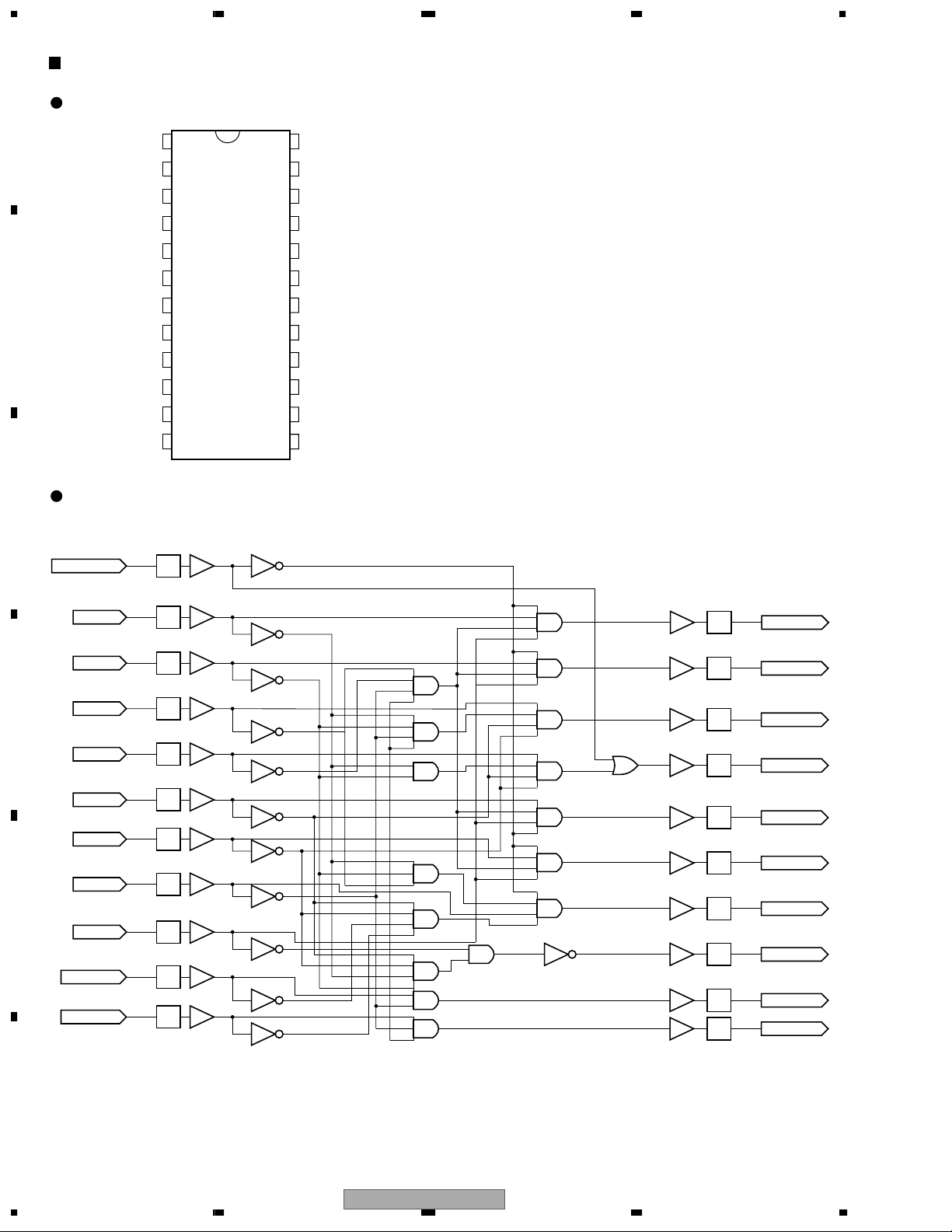
1234
PE1013B (Y DRIVEASSY : IC2006)
Drive Protect PLD
A
Pin Assignment (Top View)
B
C
I
I
I
I
I
I
I
I
I
I
GND
Block Diagram
sus_mute_in
124I/CLK
CC
V
I/O/Q
I/O/Q
I/O/Q
I/O/Q
I/O/Q
I/O/Q
I/O/Q
I/O/Q
I/O/Q
I/O/Q
I12 13
1
1_64
1_63
ysusbin
ysusuin
D
ysusdin
ysusgin
ypru1in
ypru2in
yofsin
E
ysofdin
ysusmskin
ycpmskin
11
10
2
1_7
1_20
3
1_6
1_19
4
1_5
8
1_4
6
1_3
7
1_2
5
1_1
1_10
9
1_9
1_8
1_18
1_17
1_13
1_16
1_15
1_52
1_12
1_11
1_23
1_26
1_53
1_54
1_33
1_56
1_55
1_37
1_49
1_62
1_61
1_27
1_28
1_60
1_59
1_66
1_51
23
22
21
17
19
18
20
14
16
15
1_39
1_48
1_47
1_46
1_45
1_44
1_43
1_42
1_41
1_40
ysusbout
ysusuout
ysusdout
ysusgout
ypru1out
ypru2out
yofsout
ysoftdout
ysusmskout
ycpmskout
F
94
PDP-503PC
1234
Page 95

5678
Pin Function (1/2)
M30624FGAFP (DIGITAL VIDEO ASSY : IC1207)
Module Microcomputer
.oNemaNniPnoitcnuF
1DXT retupmocorcimlenapahtiwnoitacinummocroftuptuoatadenil3laireS
2KLC retupmocorcimlenapahtiwnoitacinummocrofkcolcenil3laireS
3CNlanimretCN
4CNlanimretCN
5CNlanimretCN
6CNlanimretCN
7CNlanimretCN
8ETYB )DNGtcennocdnadesunumaI(tupnignilffuhserhtdiwsubatadlanretxeehT
9SSVNC nwod-llup,yllausu,V5,etona(etonmargorprofylppusrewopA
01NICXlanimretCN
11TUOCXlanimretCN
21TESERlanimrettupniteserA
31TUOXlanimrettuptuokcolC
41SSVDNG
51NIXlanimrettupnikcolC
61CCVrewopybdnatsV5
71IMN .pullupeldnahtI,desunusilanimretnoitpurretniIMNaesuaceB
81MERtupnilangisRSehT
91UP_QER )noitisiuqcaretemeslupeht(retupmocorcimlenapamorfdnamednoitacinummocA
02GRT_WS/hcraesNO/FFOhctiwsniaM
12CNlanimretCN
22CNlanimretCN
32CNlanimretCN
42FFO_CA .noitaitnereffidYSSAylppusrewopdnahcraesFFOrewopCA
52REGGIRT_DPhcraesnwodrewoP
62CNlanimretCN
72CNlanimretCN
82CNlanimretCN
92LCS YSSAylppusrewophtiwnoitacinummocCII,MORPEE
03ADS YSSAylppusrewophtiwnoitacinummocCII,MORPEE
131DXT)etonmargorpa(edistuoehthtiwnoitacinummoC
231DXR)etonmargorpa(edistuoehthtiwnoitacinummoC
331KLC)etonmargorpa(edistuoehthtiwnoitacinummoC
431YSUB)etonmargorpa(edistuoehthtiwnoitacinummoC
530DXT )cte,YSSABGRniniamsretupmocorcim(YSSAedistuohtiwnoitacinummoC
630DXR )cte,YSSABGRniniamsretupmocorcim(YSSAedistuohtiwnoitacinummoC
73CNlanimretCN
83ETUM_A/DM_QER
metsysoidua/)retupmocorcimniamaottseuqera(dnamednoitacinummocC232
etum
93CNlanimretCN
04CNlanimretCN
14MPE)noitaxifL(etonmargorproftupniMPEehT
24CNlanimretCN
34EC_UPretupmocorcimlenaprof/selbanE
44CNlanimretCN
54GN_A/WS_DOM tupniGNmetsysoidua/tupninoitcnitsidsenihcamfoledomehT
64EC)noitaxifH(etonmargorproftupniECehT
74CTS_WS/REHTID eludomrofrevieceraidem/gnittesrehtidafohcraesylppusrewoP
84CNlanimretCN
94PTS_WS/lenapafohcraesylppusrewoP
05CNlanimretCN
56
PDP-503PC
A
B
C
D
E
F
7
8
95
Page 96

1234
Pin Function (2/2)
.oNemaNniPnoitcnuF
A
B
C
D
E
15CNlanimretCN
25YALERegnahcFFO/NOylppusrewoproftuptuoehT
35ETATSM/REWOP egnahcFFO/NOylppusrewoprofnoitamrofniretsam168IIS/tupnI
45CNlanimretCN
55NP_EWetonretupmocorcimlenaproflortnocetatsreffuB
650DM tuptuoegnahcnoitarepofoedomretupmocorcimlenapehT
752DM tuptuoegnahcnoitarepofoedomretupmocorcimlenapehT
85EWF tuptuolangislortnocetonmargorpretupmocorcimlenapehT
95UP_TSRtuptuoteserretupmocorcimlenapehT
06ETUM_NPtupnietumlenapehT
16CNlanimretCN
26CCVrewopybdnatsV5
36CNlanimretCN
46SSVDNG
56CNlanimretCN
66CNlanimretCN
76LCS_A/metsysoiduarofkcolcCII
86ADS_A/metsysoiduarofatadCII
96ETUM_DPAseiressserddafolangisetumA
07DP_K_RDAtupniDPmetsysyrotallicsosserddaehT
17DP_RDAtupniDPseiressserddaehT
27DP_CCDtupniDPmetsysylppusrewopehT
37CNlanimretCN
47CNlanimretCN
572TSRhcraesteserretupmocorcimlenaP
67CNlanimretCN
77LCS_CDD/revieceraidemahtiwnoitacinummocCII
87ADS_CDD/revieceraidemahtiwnoitacinummocCII
97CNlanimretCN
08CNlanimretCN
18TED_WEDtupnirosnesnoitasnednocwedehT
28CNlanimretCN
38CNlanimretCN
48CNlanimretCN
58CNlanimretCN
68G_DEL )eludomlenapaniYSSAecafretninoDEL(gnithgilDELneerG
78R_DEL )eludomlenapaniYSSAecafretninoDEL(gnithgilDELdeR
88CNlanimretCN
98YSUB retupmocorcimlenapamorflangisgnitibihni/noissimrepnoitacinummoC
09CNlanimretCN
19CNlanimretCN
291YEK_F/tupniYEKtnorfehT
392YEK_F/2SLP_XAM egnahcnoitarepofoedomgnittesssenthgirbroftupniYEKtnorf/lanimretehT
491PMETrosneserutarepmetroftupniD/AehT
59MKCC/?SLP_XAM egnahcnoitarepofoedomgnittesssenthgirbrofhcraesnoitcennoc/lanimreT
69SSVAnoisrevnocDArofDNG
79TS_MPnoitcnitsidsenihcamfoledomroftupniD/AehT
89FERVnoisrevnocDArofegatlovecnerefeR
99CCVAnoisrevnocDArofrewopybdnatsV5
001DXR retupmocorcimlenapahtiwnoitacinummocrofyrtneatadenil3laireS
F
96
PDP-503PC
1234
Page 97
5678
Pin Function (1/7)
PD6358A (DIGITAL VIDEO ASSY : IC1301, IC1401)
Picture Improved IC
.oNemaNniPnoitcnuF
1SSVDNG
26OTSET)desunu(lanimrettuptuotseT
3KLCDSODSOroftupniKLCehT
4TSTT)desunu(lanimrettupnitseT
5IDDVylppusrewopV5.2
610-EDDVOylppusrewopV3.3
70OGA)langisG(tuptuoatadsserddA
8IDDVylppusrewopV5.2
92OGA)langisG(tuptuoatadsserddA
013OGA)langisG(tuptuoatadsserddA
114OGA)langisG(tuptuoatadsserddA
21IDDVylppusrewopV5.2
316ORA)langisR(tuptuoatadsserddA
417OGA)langisG(tuptuoatadsserddA
51IDDVylppusrewopV5.2
619ORA)langisR(tuptuoatadsserddA
719OBA)langisB(tuptuoatadsserddA
81IDDVylppusrewopV5.2
912OKLCRDA)trapreppulenaprof(tuptuoKLCsserddaehT
0221ORA)langisR(tuptuoatadsserddA
1231ORA)langisR(tuptuoatadsserddA
2241OGA)langisG(tuptuoatadsserddA
3251OGA)langisG(tuptuoatadsserddA
4261ORA)langisR(tuptuoatadsserddA
5271ORA)langisR(tuptuoatadsserddA
62SSVDNG
7271OBA)langisB(tuptuoatadsserddA
8271OGA)langisG(tuptuoatadsserddA
9281OGA)langisG(tuptuoatadsserddA
0391OBA)langisB(tuptuoatadsserddA
1351TADUsubatadretupmocorciM
2321TADUsubatadretupmocorciM
339TADUsubatadretupmocorciM
435TADUsubatadretupmocorciM
5360-EDDVOylppusrewopV3.3
63PLPAlangisreggirttuptuoeulavLPA
7380-EDDVOylppusrewopV3.3
83IB5SCtupnitcelespihcehT
93IB4SCtupnitcelespihcehT
0431IRDAUsubsserddaretupmocorciM
149IRDAUsubsserddaretupmocorciM
246IRDAUsubsserddaretupmocorciM
342IRDAUsubsserddaretupmocorciM
441IRDAUsubsserddaretupmocorciM
542ITSET)desunu(lanimrettupnitseT
640TIB)tib0eht(tuptuooNdleifbusehT
7411-EDDVOylppusrewopV3.3
844OTSET)desunu(lanimrettuptuotseT
9493ORA)langisG(tuptuoatadsserddA
0583OGA)langisG(tuptuoatadsserddA
56
PDP-503PC
A
B
C
D
E
F
7
8
97
Page 98
1234
Pin Function (2/7)
.oNemaNniPnoitcnuF
A
B
C
D
E
15SSVDNG
2573OBA)langisB(tuptuoatadsserddA
3563OBA)langisB(tuptuoatadsserddA
4563ORA)langisR(tuptuoatadsserddA
5543OBA)langisB(tuptuoatadsserddA
654OKLCRDA)trapmottoblenaprof(tuptuoKLCsserddaehT
7533OGA)langisG(tuptuoatadsserddA
8523OGA)langisG(tuptuoatadsserddA
9513OGA)langisG(tuptuoatadsserddA
0603OGA)langisG(tuptuoatadsserddA
1692OGA)langisG(tuptuoatadsserddA
26IDDVylppusrewopV5.2
3672OBA)langisB(tuptuoatadsserddA
4662OGA)langisG(tuptuoatadsserddA
56IDDVylppusrewopV5.2
6642OGA)langisG(tuptuoatadsserddA
76IDDVylppusrewopV5.2
8622OBA)langisB(tuptuoatadsserddA
96IDDVylppusrewopV5.2
0712ORA)langisR(tuptuoatadsserddA
1702ORA)langisR(tuptuoatadsserddA
27IDDVylppusrewopV5.2
3741-EDDVOylppusrewopV3.3
47IDTtupniGATJehT
579IBR)tibhtnineht(tupnilangistcepsaBerutcipRehT
67SSVDNG
778IBR)tibhthgieeht(tupnilangistcepsaBerutcipRehT
876IBR)tibhtxiseht(tupnilangistcepsaBerutcipRehT
974IBR)tibhtruofeht(tupnilangistcepsaBerutcipRehT
0890-SSVODNG
18BTSRtupniteseR
288IBG)tibhthgieeht(tupnilangistcepsaBerutcipGehT
3881-EDDVOylppusrewopV3.3
485IBG)tibhtfifeht(tupnilangistcepsaBerutcipGehT
582IBG)tibdnoceseht(tupnilangistcepsaBerutcipGehT
68IEDtupnilangisED
786IBB)tibhtxiseht(tupnilangistcepsaBerutcipBehT
883IBB)tibdrihteht(tupnilangistcepsaBerutcipBehT
98IDVtupnilangisDV
09IDHtupnilangisDH
196IAR)tibhtxiseht(tupnilangistcepsaAerutcipRehT
292IAR)tibdnoceseht(tupnilangistcepsaAerutcipRehT
390ITSET)desunu(lanimrettupnitseT
4911-SSVODNG
597IAGtibhtneveseht(tupnilangistcepsaAerutcipGehT
693IAG)tibdrihteht(tupnilangistcepsaAerutcipGehT
790IAG)tib0eht(tupnilangistcepsaAerutcipGehT
896IAB)tibhtxiseht(tupnilangistcepsaAerutcipBehT
993IAB)tibdrihteht(tupnilangistcepsaAerutcipBehT
0010IAB)tib0eht(tupnilangistcepsaAerutcipBehT
F
98
PDP-503PC
1234
Page 99
5678
Pin Function (3/7)
.oNemaNniPnoitcnuF
1017OTSET)desunu(lanimrettuptuotseT
2015OTSET)desunu(lanimrettuptuotseT
301HDSOtupniHDSO
401KLBtupniKLBDSO
501BDSOtupnilangisBDSO
601CNlanimretCN
7011ORA)langisR(tuptuoatadsserddA
8012ORA)langisR(tuptuoatadsserddA
9013ORA)langisR(tuptuoatadsserddA
0114ORA)langisR(tuptuoatadsserddA
1115ORA)langisR(tuptuoatadsserddA
2115OBA)langisB(tuptuoatadsserddA
3117ORA)langisR(tuptuoatadsserddA
4118ORA)langisR(tuptuoatadsserddA
5118OBA)langisB(tuptuoatadsserddA
6119OGA)langisG(tuptuoatadsserddA
71101OGA)langisG(tuptuoatadsserddA
8111OKLCRDA)trapreppulenaprof(tuptuoKLCsserddA
91111OBA)langisB(tuptuoatadsserddA
02121OBA)langisB(tuptuoatadsserddA
12141ORA)langisR(tuptuoatadsserddA
22151ORA)langisR(tuptuoatadsserddA
32151OBA)langisB(tuptuoatadsserddA
42161OBA)langisB(tuptuoatadsserddA
52161OGA)langisG(tuptuoatadsserddA
62181ORA)langisR(tuptuoatadsserddA
72191OGA)langisG(tuptuoatadsserddA
82150-EDDVOylppusrewopV3.3
92131TADUsubatadretupmocorciM
03101TADUsubatadretupmocorciM
1316TADUsubatadretupmocorciM
2313TADUsubatadretupmocorciM
3310TADUsubatadretupmocorciM
43170-EDDVOylppusrewopV3.3
531RLtupnitcelesRLlenapehT
631IBDRlanimretlortnocdaerretupmocorciM
731LESKLCtupnitcelesKLC
83101IRDAUsubsserddaretupmocorciM
9317IRDAUsubsserddaretupmocorciM
0413IRDAUsubsserddaretupmocorciM
141BELCYClangislortnoctuptuoatadsserddA
2412TIB)tibdnoceseht(tuptuo.oNdleifbuS
341BTSFSlangislortnoctuptuoatadsserddA
44150-SSVODNG
5412OTSET)desunu(lanimrettuptuotseT
64183OBA)langisB(tuptuoatadsserddA
74183ORA)langisR(tuptuoatadsserddA
84173ORA)langisR(tuptuoatadsserddA
94163OGA)langisG(tuptuoatadsserddA
05153ORA)langisR(tuptuoatadsserddA
A
B
C
D
E
F
56
PDP-503PC
7
8
99
Page 100

1234
Pin Function (4/7)
.oNemaNniPnoitcnuF
A
B
C
D
E
1513OKLCRDA)trapmottoblenaprof(tuptuoKLCsserddaehT
25133OBA)langisB(tuptuoatadsserddA
35123OBA)langisB(tuptuoatadsserddA
451IDDVylppusrewopV5.2
55103OBA)langisB(tuptuoatadsserddA
651IDDVylppusrewopV5.2
75182OBA)langisB(tuptuoatadsserddA
85182ORA)langisR(tuptuoatadsserddA
95162OBA)langisB(tuptuoatadsserddA
06152OBA)langisB(tuptuoatadsserddA
16142OBA)langisB(tuptuoatadsserddA
26142ORA)langisR(tuptuoatadsserddA
36132ORA)langisR(tuptuoatadsserddA
46122ORA)langisR(tuptuoatadsserddA
56112OGA)langisG(tuptuoatadsserddA
66102OGA)langisG(tuptuoatadsserddA
761ODTlangisGATJ
861SMTlangisGATJ
9617IBR)tibhtneveseht(tupnilangistcepsaBerutcipRehT
071KCTlangisGATJ
1715IBR)tibhtfifeht(tupnilangistcepsaBerutcipRehT
2713IBR)tibdrihteht(tupnilangistcepsaBerutcipRehT
3711IBR)tibtsrifeht(tupnilangistcepsaBerutcipRehT
47161-EDDVOylppusrewopV3.3
5717IBG)tibhtneveseht(tupnilangistcepsaBerutcipGehT
67101-SSVODNG
7714IBG)tibhtruofeht(tupnilangistcepsaBerutcipGehT
8711IBG)tibtsrifeht(tupnilangistcepsaBerutcipGehT
9719IBB)tibhtnineht(tupnilangistcepsaBerutcipBehT
0815IBB)tibhtfifeht(tupnilangistcepsaBerutcipBehT
1812IBB)tibdnoceseht(tupnilangistcepsaBerutcipBehT
2819IAR)tibhtnineht(tupnilangistcepsaAerutcipRehT
3813KLC)desunu(lanimrettupniKLC
4815IAR)tibhtfifeht(tupnilangistcepsaAerutcipRehT
5811IAR)tibtsrifeht(tupnilangistcepsaAerutcipRehT
6811ITSET)desunu(lanimrettupnitseT
7819IAG)tibhtnineht(tupnilangistcepsaAerutcipGehT
8816IAG)tibhtxiseht(tupnilangistcepsaAerutcipGehT
9812IAG)tibdnoceseht(tupnilangistcepsaAerutcipGehT
0919IAB)tibhtnineht(tupnilangistcepsaAerutcipBehT
1915IAB)tibhtfifeht(tupnilangistcepsaAerutcipBehT
2912IAB)tibdnoceseht(tupnilangistcepsaAerutcipBehT
3911IAB)tibtsrifeht(tupnilangistcepsaAerutcipBehT
49110-SSVODNG
59120-SSVODNG
691GDSOtupnilangisGDSO
7910ORA)langisR(tuptuoatadsserddA
8910OBA)langisB(tuptuoatadsserddA
9911OBA)langisB(tuptuoatadsserddA
0022OBA)langisB(tuptuoatadsserddA
F
100
PDP-503PC
1234
 Loading...