

Philips (Now NXP) PMBS3904 Schematic [ru]
DISCRETE SEMICONDUCTORS
DATA SH EET
ook, halfpage
M3D088
PMBS3904
NPN general purpose transistor
Product specification
Supersedes data of 1997 May 20
1999 Apr 22
Philips Semiconductors Product specification
NPN general purpose transistor PMBS3904
FEATURES
• Low current (max. 100 mA)
• Low voltage (max. 40 V).
APPLICATIONS
• General purpose switching and amplification, e.g.
telephony and professional communication equipment.
DESCRIPTION
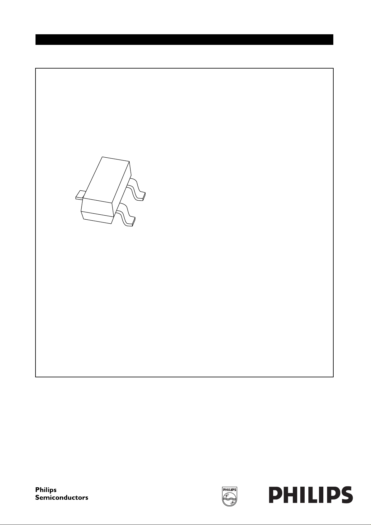
NPN transistor in a plastic SOT23 package.
PNP complement: PMBS3906.
MARKING
TYPE NUMBER MARKING CODE
PMBS3904 ∗O4
Note
1. ∗ = p : Made in Hong Kong.
∗ = t : Made in Malaysia.
(1)
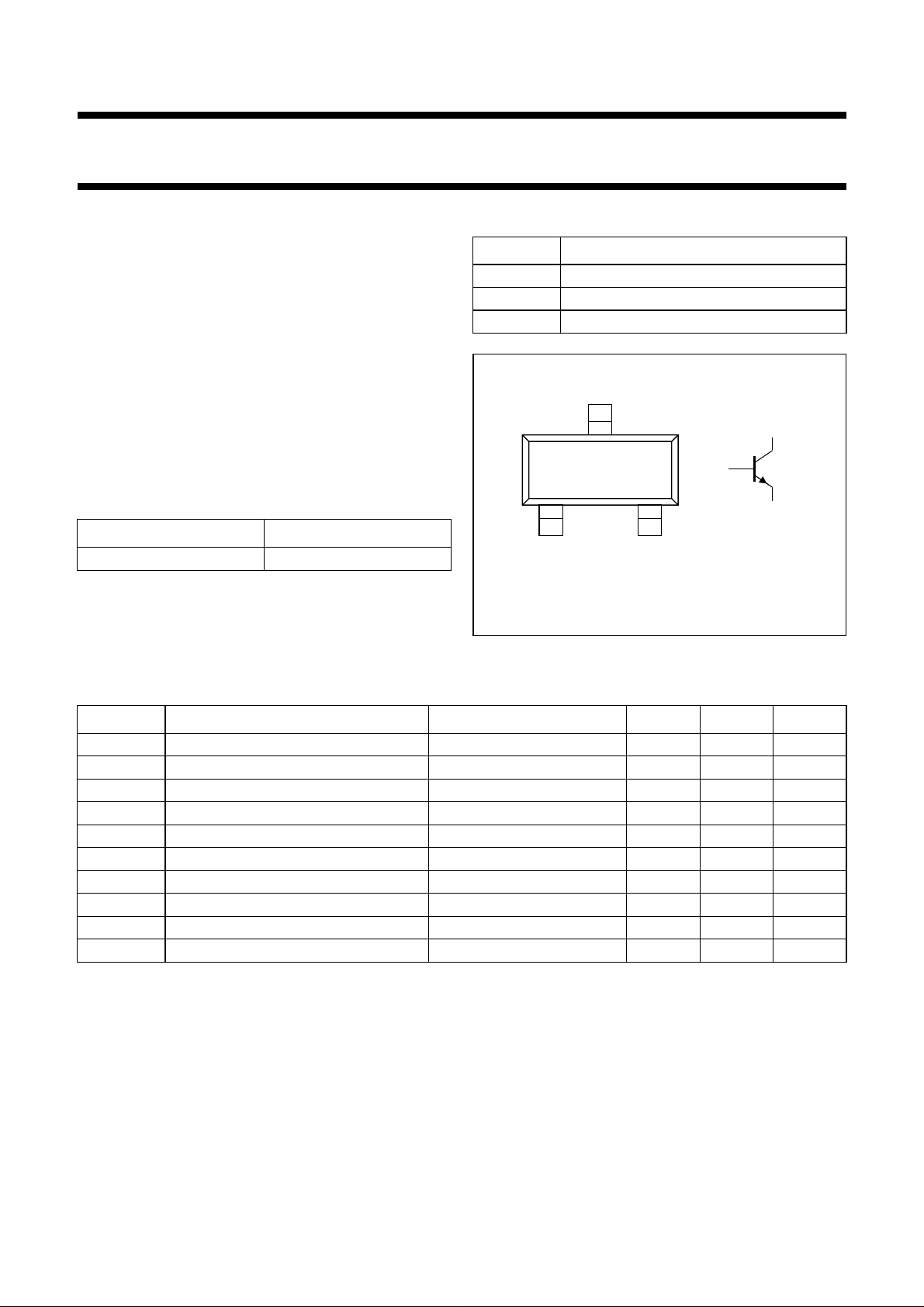
PINNING
PIN DESCRIPTION
1 base
2 emitter
3 collector
handbook, halfpage
Top view
3
21
MAM255
Fig.1 Simplified outline (SOT23) and symbol.
3
1
2
LIMITING VALUES
In accordance with the Absolute Maximum Rating System (IEC 134).
SYMBOL PARAMETER CONDITIONS MIN. MAX. UNIT
V
CBO
V
CEO
V
EBO
I
C
I
CM
I
BM
P
tot
T
stg
T
j
T
amb
collector-base voltage open emitter − 60 V
collector-emitter voltage open base − 40 V
emitter-base voltage open collector − 6V
collector current (DC) − 100 mA
peak collector current − 200 mA
peak base current − 200 mA
total power dissipation T
≤ 25 °C − 250 mW
amb
storage temperature −65 +150 °C
junction temperature − 150 °C
operating ambient temperature −65 +150 °C
1999 Apr 22 2
Philips Semiconductors Product specification
NPN general purpose transistor PMBS3904
THERMAL CHARACTERISTICS
SYMBOL PARAMETER CONDITIONS VALUE UNIT
R
th j-a
Note
1. Transistor mounted on an FR4 printed-circuit board.
CHARACTERISTICS
=25°C unless otherwise specified.
T
amb
SYMBOL PARAMETER CONDITIONS MIN. MAX. UNIT
I
CBO
I
EBO
h
FE
V
CEsat
V
BEsat
C
c
C
e
f
T
F noise figure I
thermal resistance from junction to ambient note 1 500 K/W
collector cut-off current IE= 0; VCB=30V − 50 nA
emitter cut-off current IC= 0; VEB=5V − 50 nA
DC current gain VCE= 1 V; note 1; (see Fig.2)
= 0.1 mA 40 −
I
C
I
= 1 mA 70 −
C
= 10 mA 100 300
I
C
I
=50mA 60 −
C
I
= 100 mA 30 −
C
collector-emitter saturation
voltage
IC= 10 mA; IB=1mA − 200 mV
I
= 50 mA; IB=5mA − 300 mV
C
base-emitter saturation voltage IC= 10 mA; IB= 1 mA 650 850 mV
I
= 50 mA; IB=5mA − 950 mV
C
collector capacitance IE=ie= 0; VCB=5V; f=1MHz − 4pF
emitter capacitance IC=ic= 0; VEB= 0.5 V; f = 1 MHz − 12 pF
transition frequency IC= 10 mA; VCE= 20 V; f = 100 MHz 180 − MHz
= 100 µA; VCE=5V; RS=1kΩ;
C
− 5dB
f = 10 Hz to 15.7 kHz
Switching times (between 10% and 90% levels); (see Fig.3)
t
on
t
d
t
r
t
off
t
s
t
f
turn-on time I
delay time − 50 ns
rise time − 60 ns
= 10 mA; I
Con
I
= − 1 mA; VCC=3V;
Boff
VBB= −1.9 V
turn-off time − 1200 ns
storage time − 1000 ns
fall time − 200 ns
Note
1. Pulse test: t
≤ 300 µs; δ≤0.02.
p
1999 Apr 22 3
Bon
= 1 mA;
− 110 ns
 Loading...