

Philips MX1015D, МХ-1055D Service Manual
Service Manual
DVD Surround Receiver
Service
Service
Service
MX1015D/37
MX1055D/37S
For Repair infromation on the Sub-woofer please refer to
Type/version package on page 1-2
TABLE OF CONTENTS
Location of pc boards & Type/version package.........1-2
Technical Specifications .............................................1-3
Measurement setup....................................................1-4
Service Aids, Safety Instruction, etc. ..........................1-5
Repair Instructions......................................................2-1
Disassembly Instructions & Service positions .............. 3
Set Block & Wiring diagram...........................................4
PSU Board .....................................................................5
Front Board....................................................................6
Tuner Board (For information only) ............................... 7
AV Output Board......................................................... 8A
DVD Module (For information only)...............................9
Audio Switch Board .....................................................10
Video Switch Board ..................................................... 11
Power Amplifier Board ................................................. 12
Pro-Logic Board:.......................................................... 13
Set Mechanical Exploded view & parts list .................1 4
Page
CLASS 1
©
Copyright 2001 Philips Consumer Electronics B.V. Eindhoven, The Netherlands
All rights reserved. No part of this publication may be reproduced, stored in a retrieval system or
transmitted, in any form or by any means, electronic, mechanical, photocopying, or otherwise
without the prior permission of Philips.
Published by KC 0128 Service Audio Printed in The Netherlands Subject to modification
Version 1.0
LASER PRODUCT
GB
3139 785 22920
LOCATION OF PC BOARDS
1-2
Main Amplifier
Board
DVD Mech
Loader
DVD Main
Board
PSU
Board
Front Board
(behind the
metal panel)
Pro-Logic
Board
VERSION PACKAGE:
Package Unit: /37 /37S
Center Unit DFR1500/17 x
Center Unit DFR1600/17S x
Sub-woofer SW090/17 x 3139 785 22910
Sub-woofer SW986/17S x 3139 785 22880
Satellite Speakers CS985/17 x
Satellite Speakers CS990/17S x
Tuner
Board
Type /Versions: MX1015D MX1055D For repair of Sub-woofer Unit
Audio Switch
Board
Video Switch
Board
see Service Manual with
12NC given below
AV Output
Board

SPECIFICATIONS
1-3
GENERAL:
Mains voltage : 120V
Mains frequency : 60Hz
Power consumption : < 4W at Standby
< 450W Maximum
Clock accuracy : < 3 seconds/day
Dimension (w x h x d) : 435 x 140 x 430mm
TUNER:
FM
Tuning range : 87.5-108MHz
Grid : 100kHz
IF frequency : 10.7MHz ± 70kHz
Aerial input : 300Ω click fit
Sensitivity at 26dB S/N : < 6µV
Selectivity at 600kHz bandwidth : > 25dB
Image rejection : > 25dB
Distortion at RF=1mV, dev. 75kHz : < 3%
Crosstalk at RF=1mV, dev. 75kHz : > 18dB
Stereo threshold : < 28dB
MW
Tuning range : 530-1700kHz
Grid : 10kHz
IF frequency : 450kHz ± 3kHz
Aerial input : Frame aerial
Sensitivity at 26dB S/N : < 3.2mV/M
Selectivity at 18kHz bandwidth : > 20dB
IF rejection : > 38dB
Image rejection : > 28dB
Distortion at RF=50mV, m=80% : < 5%
DVD SECTION:
Reference:
NTSC Test Disc : ABEX - TDV540
PAL Test Disc : PHILIPS - LVP10.01
Load Impedance : 75
Ω
Laser Type : 650 ± 5nm
Disc Diameter : 8cm / 12cm
Play time (12cm):
Single Layer : 2.12hr
Dual Layer : 4.01hr
2 Sides, Single Layer : 4.26hr
2 sides, Dual Layer : 8.02hr
Video Decoding : MPEG2
Video DAC : 10 Bits
Signal System : PAL / NTSC
Video Format : 4:3 / 16:9
Video S/N ratio : 56dB min.
Audio DAC : 24 Bits / 96kHz
Video Output:
CVBS Output : 1V
S-Video Output Y : 1V
C : 286mV
± 10%,
p-p
± 10%
p-p
± 10%
p-p
Digital Output : Coaxial & Optical
1)
8Ω, 40Hz - 20kHz, 0.7% THD
AMPLIFIER:
Reference Output = 1W @ 8Ω
Output power: Stereo L/R : 2 x 60W FTC
Surround L/R : 2 x 60W FTC
Center : 60W FTC
1)
Distortion at 1kHz, rated power - 6dB : < 0.7%
Signal to Noise Ratio : > 65dB CCIR
Frequency response : 20Hz - 20kHz / ± 1dB
Treble control : 10kHz / ± 10dB
Bass control : 100Hz / ± 10dB
VCR / TV / CDR input : 460mV ± 70mV
Sub-woofer output (without load) : > 3V
Digital output (IEC958, 44.1kHz) : 500mV ± 20%
1)
1)
1-4
Tuner AM Band
SSG=Standard Signal Generator
AM/FM SSG
LOOP
OUT
Tuner FM Band
SSG=Standard Signal Generator
AM/FM STEREO
SSG
PADHEAD
AM LOOP
ANT
AM ANT
DUT
OUT
LOAD
8 OHM
L
FL
LOAD
8 OHM
L
SCOPE
R
2 CH
AC LEVEL METER
2 CH
DISTORTION
METER
2 CH
FR
S-Video/Scart/Digital Output
SCOPE
AC LEVEL
METER
UL/S-VIDEO
CE/SCART
AC LEVEL
METER
R
L
REC
OUT
OPT
COAX
DIGITAL
OUT
L
DTS
DECODER
SCOPE
2 CH
AC METER LEVEL
2 CH
R
DUT
SCOPE
R
2 CH
AC LEVEL METER
2 CH
DISTORTION
METER
2 CH
CD/DVD/C-VIDEO OUTPUT
NTSC/PAL
VIDEO SIGNAL
GENERATOR
C-VIDEO IN
MONITOR
REC OUT
VIDEO
SCOPE
SUB
OUT
FR
SR
FL
SL
C
DUT
AC
LEVEL
METER
SL/SR
CENTER
FL/FR
SCOPE
SWITCH
LOAD
8 OHM
LEVEL
DISTORTION
METER
2 CH
SCOPE
2 CH
Balance EQ Power
SCOPE
AUDIO STEREO
GENERATOR
AC
L
R
LEVEL
METER
L
R
SUB
OUT
IN
DUT
FR
FM ANT
FL
DUT
LOAD
8 OHM
SL/SR
CENTER
FL/FR
FR
FL
C
SR
SL
SWITCH
LEVEL
DISTORTION
METER
2 CH
SCOPE
2 CH
SERVICE AIDS
Service Tools:
Universal Torx driver holder .................................. 4822 395 91019
Torx bit T10 150mm ............................................. 4822 395 50456
Torx driver set T6 - T20......................................... 4822 395 50145
Torx driver T10 extended ...................................... 4822 395 50423
ESD Equipment:
Anti-static table mat - large 1200x650x1.25mm ... 4822 466 10953
Anti-static table mat - small 600x650x1.25mm..... 4822 466 10958
Anti-static wristband .............................................. 4822 395 10223
Connector box (1MΩ) ............................................ 4822 320 11307
Extension cable
(to connect wristband to conn. box).................. 4822 320 11305
Connecting cable
(to connect table mat to conn. box) .................. 4822 320 11306
Earth cable (to connect product to mat or box) .... 4822 320 11308
1-5
Complete kit ESD3
(combining all above products) ......................... 4822 320 10671
Wristband tester .................................................... 4822 344 13999
HANDLING CHIP COMPONENTS
WARNING
GB
All ICs and many other semi-conductors are
susceptible to electrostatic discharges (ESD).
Careless handling during repair can reduce life
drastically.
When repairing, make sure that you are
connected with the same potential as the mass
of the set via a wrist wrap with resistance.
Keep components and tools also at this
potential.
F
ATTENTION
Tous les IC et beaucoup d’autres
semi-conducteurs sont sensibles aux
décharges statiques (ESD).
Leur longévité pourrait être considérablement
écourtée par le fait qu’aucune précaution n’est
prise à leur manipulation.
Lors de réparations, s’assurer de bien être relié
au même potentiel que la masse de l’appareil et
enfiler le bracelet serti d’une résistance de
sécurité.
Veiller à ce que les composants ainsi que les
outils que l’on utilise soient également à ce
potentiel.
1-6
ESD
D
WARNUNG
Alle ICs und viele andere Halbleiter sind
empfindlich gegenüber elektrostatischen
Entladungen (ESD).
Unsorgfältige Behandlung im Reparaturfall kan
die Lebensdauer drastisch reduzieren.
Veranlassen Sie, dass Sie im Reparaturfall über
ein Pulsarmband mit Widerstand verbunden
sind mit dem gleichen Potential wie die Masse
des Gerätes.
Bauteile und Hilfsmittel auch auf dieses gleiche
Potential halten.
WAARSCHUWING
NL
Alle IC’s en vele andere halfgeleiders zijn
gevoelig voor electrostatische ontladingen
(ESD).
Onzorgvuldig behandelen tijdens reparatie kan
de levensduur drastisch doen verminderen.
Zorg ervoor dat u tijdens reparatie via een
polsband met weerstand verbonden bent met
hetzelfde potentiaal als de massa van het
apparaat.
Houd componenten en hulpmiddelen ook op
ditzelfde potentiaal.
I
AVVERTIMENTO
Tutti IC e parecchi semi-conduttori sono
sensibili alle scariche statiche (ESD).
La loro longevità potrebbe essere fortemente
ridatta in caso di non osservazione della più
grande cauzione alla loro manipolazione.
Durante le riparazioni occorre quindi essere
collegato allo stesso potenziale che quello della
massa dell’apparecchio tramite un braccialetto
a resistenza.
Assicurarsi che i componenti e anche gli utensili
con quali si lavora siano anche a questo
potenziale.
GB
Safety regulations require that the set be restored to its original
condition and that parts which are identical with those specified,
be used.
NL
Veiligheidsbepalingen vereisen, dat het apparaat bij reparatie in
zijn oorspronkelijke toestand wordt teruggebracht en dat onderdelen,
identiek aan de gespecificeerde, worden toegepast.
F
Les normes de sécurité exigent que l’appareil soit remis à l’état
d’origine et que soient utiliséés les piéces de rechange identiques
à celles spécifiées.
D
Bei jeder Reparatur sind die geltenden Sicherheitsvorschriften zu
beachten. Der Original zustand des Geräts darf nicht verändert werden;
für Reparaturen sind Original-Ersatzteile zu verwenden.
“Pour votre sécurité, ces documents
doivent être utilisés par des spécialistes agréés, seuls habilités à réparer
votre appareil en panne”.
CLASS 1
LASER PRODUCT
GB
Invisible laser radiation when open.
Avoid direct exposure to beam.
Osynlig laserstrålning när apparaten är öppnad och spärren
är urkopplad. Betrakta ej strålen.
Warning !
S
Varning !
3122 110 03420
I
Le norme di sicurezza esigono che l’apparecchio venga rimesso
nelle condizioni originali e che siano utilizzati i pezzi di ricambio
identici a quelli specificati.
"After servicing and before returning set to customer perform a
leakage current measurement test from all exposed metal parts to
earth ground to assure no shock hazard exist. The leakage current
must not exceed 0.5mA."
Varoitus !
SF
Avatussa laitteessa ja suojalukituksen ohitettaessa olet alttiina
näkymättömälle laserisäteilylle. Älä katso säteeseen!
DK Advarse !
Usynlig laserstråling ved åbning når sikkerhedsafbrydere er
ude af funktion. Undgå udsaettelse for stråling.
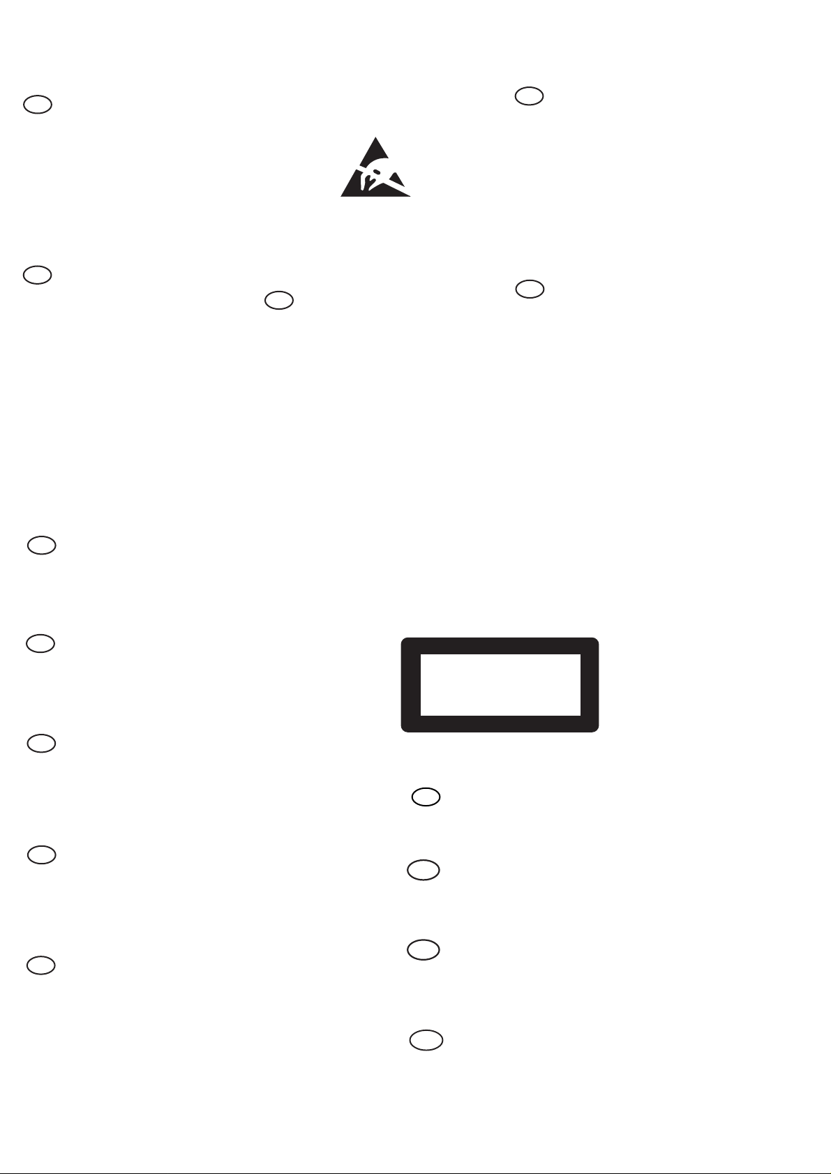
MX10xxD REPAIR CHART
MX10xxD Repair Chart
Main Unit
2-1 2-1
A
Audio output
No sound
A
Audio output
No sound
Video output
No picture
CB
No sound &
picture output
Yes
Check Audio BD power
supply UA1
Pin19,12=+/-12V, Pin4,27
have signal or not
Check Front BD CPU/U5
Pin1/SCLK
Pin63/SCE
Pin64/SD1
Yes
Audio BD UA1
Pin13/CE
Pin14/D1
Pin15/CL
Yes
Prologic BD U3
Pin22/D1
Pin23/CLK
Pin24/CE
No
No
No Signal
Check Audio
BD/QA1,QA2
Possible UA1 bad
cause
Possible UA1 bad
cause or U5
Possible U3 bad
cause
Yes
Check CBL4B
Pin4 Tuner
EN=4.7V
No
Check Front BD
CPU/U5
Pin49=4.7V
Possible CPU
bad cause
Possible cause
U3 bad/damage
No
No
Tuner no
output
Check to Tuner BD
power supply
Yes
Check to Tuner BD
Control data signal
Audio BD CBL 12/Pin
9.10.11.12.13.14
No
Check the data from Front
BD CPU U5/Pin 50/ST
Pin 51/PLL SD
Pin 52/PLL CLK
Pin 53/PLL DI
Pin 54/PLL D0
Pin 55/PLL CE
No data
Possible CPU U5 bad
cause damage
Check Prologic BD
U3/pin3,9,14,17,1,2
U4/pin2,19,7,14 signal
Yes
Check Prologic BD MUTE
circuit Q15 electrode
B>0.7VDC
Yes
Check Prologic BD
U3,U2,U5,U1 power supply
working
No
No
All channel no sound
Check all cable is loose
or bad INT
Yes
Check the Fuse F1 &
F2(Amp BD)
Yes
Check the power Relay
(PSU BD) is working or
not
working
Check PSU BD CBL02A
Pin 1=5V, Pin 3=12V,
Pin 5 = -12V
Yes
Check AMP BD channel
output Relay RL1,2,3 is
working or not
Not work
Check Front BD CPU/U5
Pin5=4.8VDC
No
Check R20/10K (+5V up tug)
or CPU/U5 damage
Repair power supply
circuit
No
Re-insert and fix the
No
Change the fuse
12A/250VAC
Not working
U5/Pin2=4.8VDC or change
Check the channel unnormal
operation power AMP section
cable
Possible
Prologic BD
U3 damage
Check PSU BD Q4
electrode B=0V
No
Check PSU BD
CBL03A PWR
SW/Pin6=4.8V
No
Check Front BD CPU
CPU/UPD780023QFP
Check protection circuit
(AMP BD)
IC/U6 Pin6=0VDC
Pin1=0VDC, Pin2<0.7VDC
Pin 2 No
Check power AMP IC
U1,2,3,4,5/Pin3=0VDC
No
Yes
Yes
Yes
Pin 1 No
DVD Audio
no output
Check Prologic BD
CBL10
5.1CH Input
Repair/Replace DVD
Main BD
Change Q4/8550
Change Q2/9014
Check power supply +/-36V
Q2/9015, Q3/9014

MX10xxD REPAIR CHART
2-22-2
B
Check
QV1, QV2,
QV3 & QV4
A/V SCART BD (CE)
PS1/pin19 CVBS-OUT
Yes
C-Video
no output
Check Video
BD power supply UV3
pin11,10=9V
pin5=-9V
Yes
Check
UV3/pin14,16
V-out
No
Check Video
BD UV3 Control Data
Pin6/CE, Pin7/DI,
Pin8/CLK
No
Possible Audio BD
CBL13A/Pin1/CE,
Pin2/DI, Pin3/CLK,
connection bad
Yes
No
Video Output
Check Video BD
UV1/79L09
UV2/78L09
+/-9V
No
Check Audio BD
CBL13B
Pin4=12V
Pin6=-12V
Possible
UV3 bad
cause
No signal
DVD
S-Video (UL)
SCART Video (CE)
no output
Check Power Supply
A/V BD (UL) CBL21B/pin2=5V
A/V SCART (CE) CBL21B/pin2=5VA
CB15/pin13=5VD
CB15/pin16=12V
Yes
Check the following:
1. CVBS Out/CB16/pin1
2. (UL) S-Video Out, Y/C, QV3, QV2/c
3. (CE) R,G,B, Out, SCART Jack
Pin 15,11,7
CVBS-Out/Pin 19
No
Check the following:
1. cable CB15 CVBS Out/Pin6
2. S-Video Y/C Pin4,5 (UL)
3. R,G,B/Pin 11,10,9 (CE)
No
Check DVD BD CPU/ICS1
CVBS OUT/Pin64
C_OUT/Pin63, Y_OUT/Pin62
R_OUT/Pin57, G_OUT/Pin56
B_OUT/Pin55
Yes
Yes
Yes
No
No
If CBL21B/Pin2 is
bad check PSU BD
If CB15 is bad check
DVD Main BD
1. Check Video BD
2. Check S-Video Connection (UL)
3. Check SCART Connection (CE)
1. CVBS Out check QV1
2. S-Video check QV2, QV3 (UL)
3. R,G,B check QN1, QN2, QN3
Check DVD Main BD
HS6 cable & connector
Check Audio BD CBL13A
Pin4=+12V
Pin6=-12V
Pin7=+5V
Check
PSU BD DB2
diode bridge
U6/7812
U7/7912
U4/7805
Yes
Yes
C
No Sound
& picture
Check Prologic BD. Video BD
Audio BD power supply. test PSU
BD CBL02A +/-12VDC, +5V
No
Check
PSU BD Fuse
F3,F4,F1
Yes
Check
PSU BD connector
JC6=20VAC
No
Check
PSU BD power
Relay is working or
not
working
Check the below data:
From Front BD Data
U5 Pin 63/SCE
Pin 64/SDI
Pin 65/SCLK
Prologic BD
U3 Pin 24/PCE
Pin 22/PDI
Pin 23/PCLK
Audio DB
UA1 Pin 13/CE
Pin 14/DI
Pin 15/CLK
Video BD
UV3 Pin 6/CE
Pin 7/DI
Pin 8/CLK
OPEN
Not Work
Change
the Fuse with
same value
Check PSU BD CBL03
Pin2/
PWR-SW=5V
No
Check
Front BD
CPU/U5/Pin48
PWR SW=5V
or CPU damage cause
Yes
Check
PSU BD
Q2/9014
Q4/9014
& RLY1
possible is CPU/ICS1/
STi5505 damage
Replace DVD Main BD
2-3 2-3
MX10xxD REPAIR CHART - DVD SECTION
MX10xxD Repair Chart
DVD Section
D
Tray cannot
opern
E
Mechanical
Noise
D
Tray cannot open
Check B600
Connector
Pin1,2=+/-6VDC
No
Check DVD BD IC60/LB1641
Pin7/Vcc=11.8VDC, Pin6/OUT=3.1VDC,
Pin5/IN=3.1VDC,
Pin7=0V During the tray is open or close
No
Check DVD BD HS5
Connector
Pin4 T_D=3.1VDC
Pin 5 R_D=3.1VDC
Yes
Check
CPU*/Pin5/SLIDER_OUT
CPU*/Pin6/SLIDER_IN
CPU*/Pin7/SLIDER_OPEN/CLOSE
Circuit
Possible CPU* damage
Replace DVD BD
F
Cannot read
Disc or
Intermittent
Possible Tray motor defective.
Yes
Proceed to open tray manually
(see Chapter 3)
Replace the DVD Loader
Repair Motor
Yes
Driver Circuit
No
Front BD CPU
U5/Pin21, 22
No
Repair the
connection
Check
circuit
Video output
No Signal
(see page 10-2)
C
No sound &
picture
DVD no
Function
(see page 10-2)
E
Mechanical noise
during playing disc
Check the Disc
is off center or not
No
Check is there
something inside the
DVD Loader or not
No
Possible DVD Loader damage
Replace the DVD Loader
*Note: BD = Board
CPU = DVD BD ICS1/STi5505
DVD BD = DVD Main Board
Yes
Yes
HG
No Sound
Analog no output
Reset the Disc
into the center
Open the tray
& check it out
JB
No Sound
Digital no output
F
Cannot read the disc
or Intermittent
Check the Disc
for dust or damage
No
Check DVD Loader
power supply: DVD BD HX1
Pin5=5.2V, Pin6=3.3V,
Pin1=8V, Pin2=12V,
Pin12=5V
Yes
Check DVD BD HX1
Pin14-X.BCLK, Pin15-X.DATA,
Pin16-X.DATAVALID, Pin17-X.ERROR
data and circuit connection
No
Possible DVD BD CPU* damage
Replace DVD BD
Yes
No
Change to other Disc
No
Repair power supply circuit
Possible DVD Loader damage
Replace Loader & test again
DVD Main Board Connector Data
1. DVD Main Board Conn. HX1
(To Mechanical Loader)
Pin
no.
Function
1
+12VT
2
+12VS
3
GND
4
GND
5
5VD
6
3.3V
7
5GND
8
GND
9
SDA
10
SCL
11
IRD2
12
5V RESET
13
GND
14
EXT BCLK
15
EXT DATA
16
EXT DATA
Note 1
Voltage
DC/V
11.9V
11.9V
0V
0V
5.0V
3.2V
0V
0V
4.7V
4.8V
3.2V
4.7V
0V
1.56V
0.25V
0.35V
VALID
17
EXT PSTART/
ERROR
18
GND
19
NC
2. DVD Main Board Conn. JP1
(To PSU Board)
Pin
no.
Function
1
NC
2
3.3V
3
5VD
4
GND
5
GND
6
5VA
7
12V
8
5GND
9
12VS
10
12VT
0V
0V
-
Note 2
Voltage
DC/V
-
3.2V
5.1V
0V
0V
5.0V
11.9V
0V
11.9V
11.9V
3. DVD Main Board Conn. HS6
(T o A/V Board)
Pin
no.
1
2
3
4
5
6
7
8
9
10
11
12
13
14
15
16
4. DVD Main Board Conn. HS5
(To Front Board)
Pin
no.
1
2
3
4
5
6
Function
12V
5VA
16/9
4/3
5VD
GND
RED
GREEN
BLUE
GND
GND
CVBS
C
Y
GND
SPDIF
GND
Function
GND
CTS
RTS
TXD
RXD
5VD
Note 3
Voltage
DC/V
11.9V
5V
4V
0V
5.0V
0V
3.2V
3.2V
3.2V
0V
0V
0.73V
0.52V
0.67V
0V
1.6V
0V
Note 4
Voltage
DC/V
0V
0V
0V
3.0V
4.9V
4.9V
Note:
1. When the voltages of conn. HX1 are as per table the problem in the Loader,
otherwise the problem is in the DVD Main board.
2. When the voltages of conn. JP1 are as per table the problem in the DVD Main board,
otherwise the problem is in the PSU board.
3. When the voltages of conn. HS6 are as per table the problem in the DVD Main board,
otherwise the problem is in the A/V board.
4. When the voltages of conn. HS5 are as per table the problem in the DVD Main board,
otherwise the problem is in the Front board.

2-4
MX10xxD REPAIR CHART - DVD SECTION
2-4
G
DVD no function
Check DVD BD power
supply JP1 connector DATA
(see page 10-3)
Yes
Software reset
Check DVD BD HX1
Pin9/SDA=4.7V, Pin10/SCL=4.7V &
Loader power supply
Check DVD BD
1. crystal XS1/27MHz
2. CPU*/pin118=27MHz
Check DVD BD HS5 connector
pin4 TXD=3.1VDC
pin5 RXD=4.9VDC
HS5 DATA (see page 10-3)
Check CPU* power supply
pin1,18,34,75,86,95,102,119,130,139,
149,159,171,184,208=3.3V
ICM4, ICM8 power supply
ICM2/pin37,1,7,25,38,44=3.3V
Yes
No
Yes
Yes
Yes
OK
No
No
No
Check PSU BD CBL03A
connector pin7 DVD
power=4.8VDC
Yes
Check PSU BD
U8, U3, U4, U5, U6
voltages
Change DVD
Loader check
Check DVD BD
1. ICS3/74HCV04 pin14=3.3V or XS1 bad
2. ICS3 damage
Replace DVD BD
No
No
Yes
Check Front BD
CPU U5/pin21,22
Check corresponding power supply
circuit or change corresponding IC
No
Possible DVD Loader damage
Replace DVD Loader
Check Front BD
CPU U5/pin2
One of the channel
no output
Check channel
mute circuit
Yes
Check channel
pre-amp circuit
Yes
Check channel
D/A change circuit
Yes
Check corresponding
channel DATA signal
pin44/pcm-out0=FL+FR
pin24/pcm-out1=C+SUB
pin21/pcm-out2=SL+SR
No
Possible CPU* damage
Replace DVD BD
No
Repair
MUTE circuit
No
Repair
pre-amp circuit
Repair
No
D/A decode
circuit
Yes
Repair
corresponding channel
supply power
H
No Sound
Analog no output
All channel
no output
Check supply power
1. CPU pin48,49 VDDA=3.3V
2. ICA7/7805/5VA (D/A change power supply)
3. QA13 (pre-amp supply +12V)
Yes
Check D/A change
CPU*/PCM_LRCLK/Pin46
/PCM_CLK/Pin45
/PCM_SCLK/Pin43
/PCM-OUT/Pin21,24,44
No
Possible CPU* damage
Replace DVD BD
No
Check RS29/RS78
is 5V or not
Yes
Check MUTE circuit
ICS1/A-MUTE/Pin199
MUTE=L
BY PASS=H
No
1. CPU* damage
2. ICA7/7805 damage
Replace DVD BD
J
No Sound
Digital no output
A/V S-Video BD (UL) QA4/electrode E
A/V SCART BD (CE) QA4/electrode E
Check
Signal output
No
Check
DVD BD CPU*/Pin47 SPDIF
Signal output
No
Possible CPU* damage
Replace DVD BD
Yes
Possible Optical or coaxial damage
or connection cable damage
Yes
Check A/V BD S-Video / SCART
QA3, QA4
Yes
Check DVD BD Flash
ICM2/39VF800A
Pin11/WE=3.1V
Pin26/CE=2.3V
Yes
Check DVD BD ICM8/ICM4
Pin34/CKE=3.1VDC, Pin14/LDOM,
Pin15/WE, Pin16/CAS,
Pin17/RAS, Pin18/CS,
Pin35/SDCLK, Pin36/VDOM
Check CIM2,ICM4,ICM8
IN or OUT DATA
Replace DVD BD
No
No
Check circuit connection
or change ICM2.
Replace DVD BD
Check circuit connection
*Note: BD = Board
CPU = DVD BD ICS1/STi5505
DVD BD = DVD Main Board
2-5
ADDITIONAL INFORMATION FOR DVD SECTION
2-5
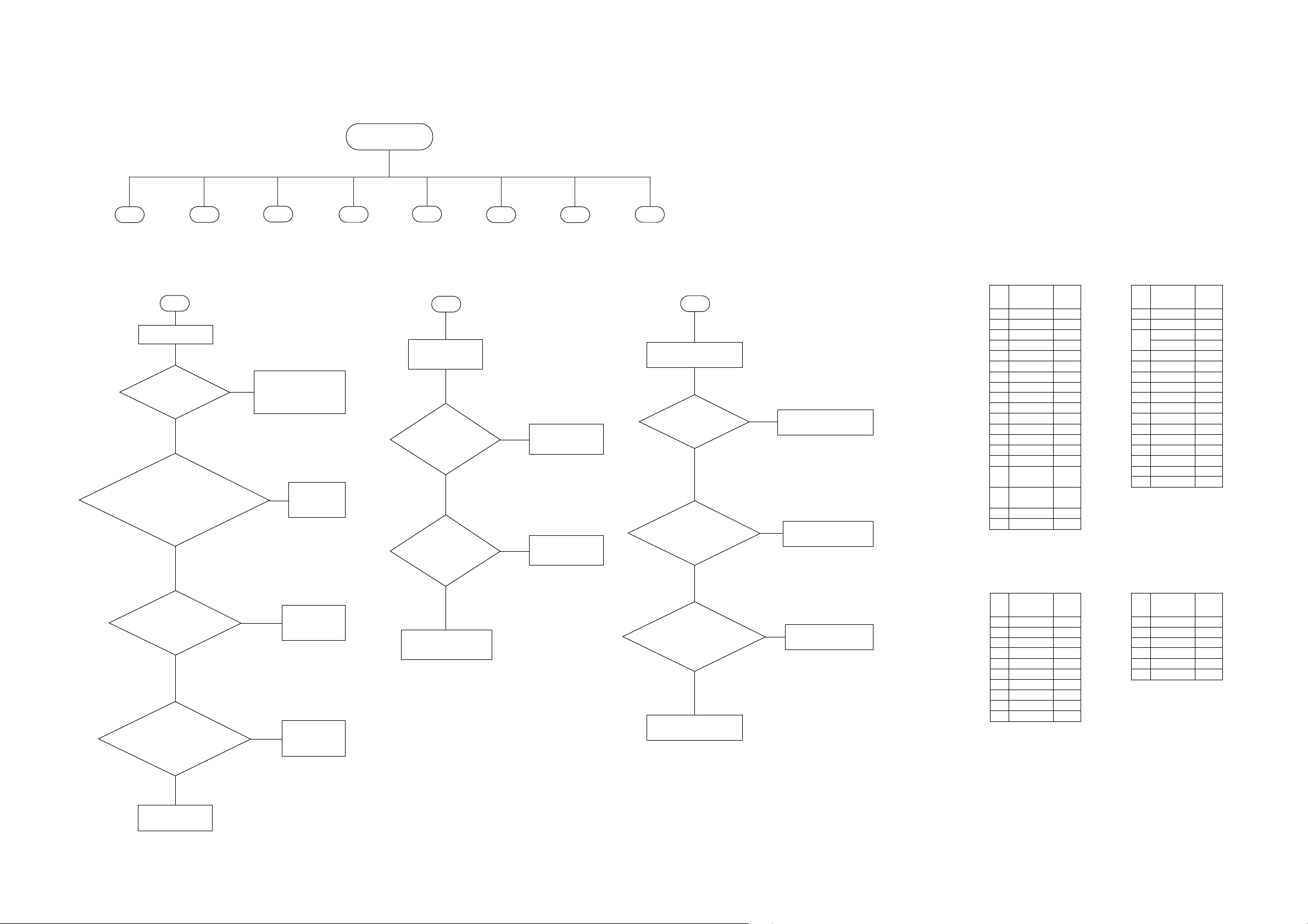
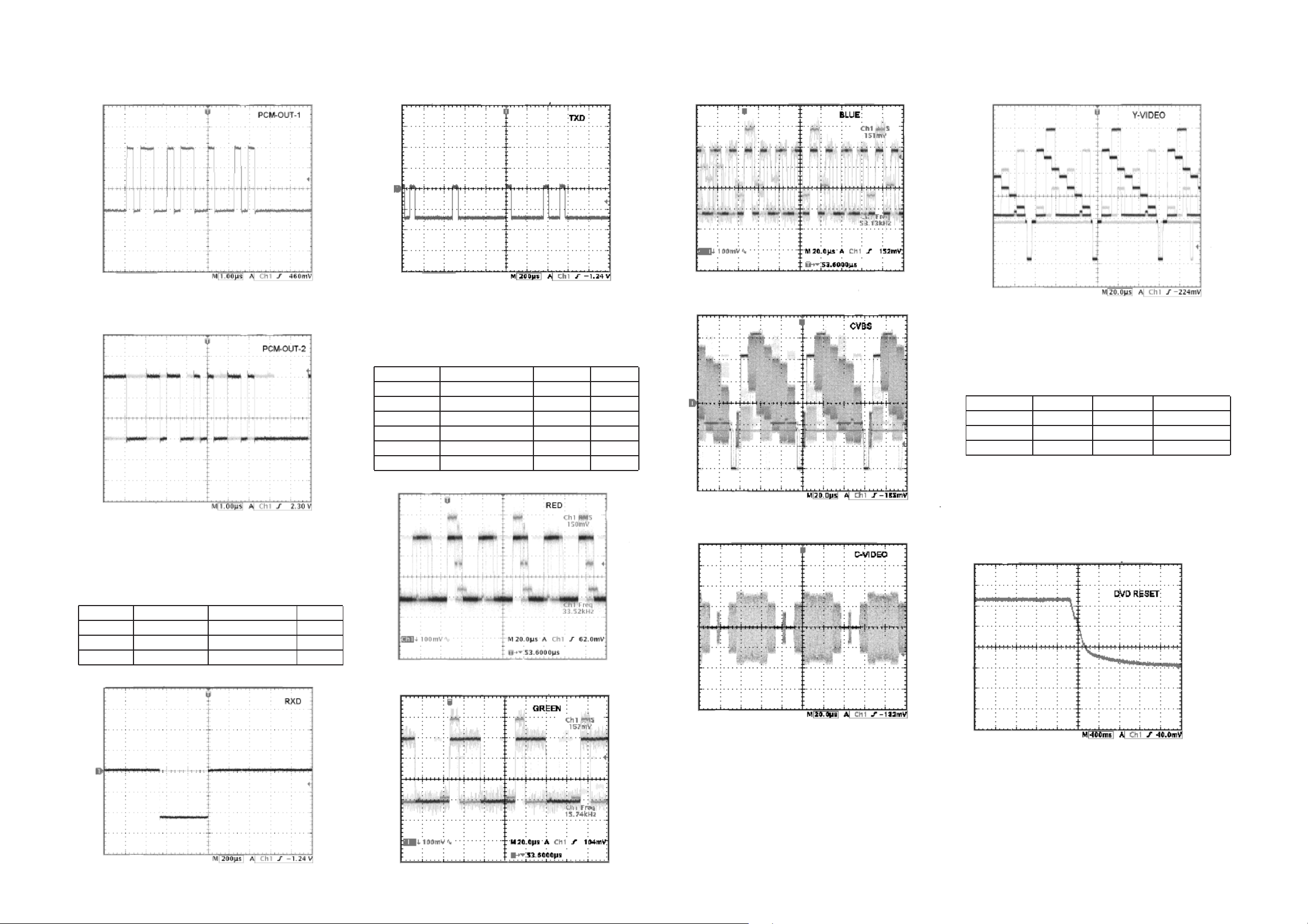
1. Clock Check
Clock name Test point Frequency Figure Remarks
27MHz Pin 118 (ICS1) 27MHz 1-a
PCM CLK Pin 45 (ICS1) 11.28MHz 1-b
Figure 1-a
3. DVD Interface
Test name Test point Figure Remarks
XERROR/P-START Pin 39 (ICS1) - High/Low
XP-CLOCK/D-VALID Pin 38 (ICS1) 3-a
XB-CLOCK/BB-CLOCK Pin 37 (ICS1) 3-b
XDATA Pin 36 (ICS1) 3-c
Figure 3-a
4. Audio LR - Clock Switch Check
Clock Frequency Test point Remarks
11.2896MHz, 0.02% Pin 46 (ICS1) 44.1kHz sample rate
12.288MHz, 0.02% Pin 46 (ICS1) 48kHz sample rate
Figure 5-b
Figure 4
Figure 1-b
2. Memory Check
Clock name Test point Frequency Figure Remarks
SD CLOCK Pin 76 (ICS1) 108MHz 2-a
Figure 3-b
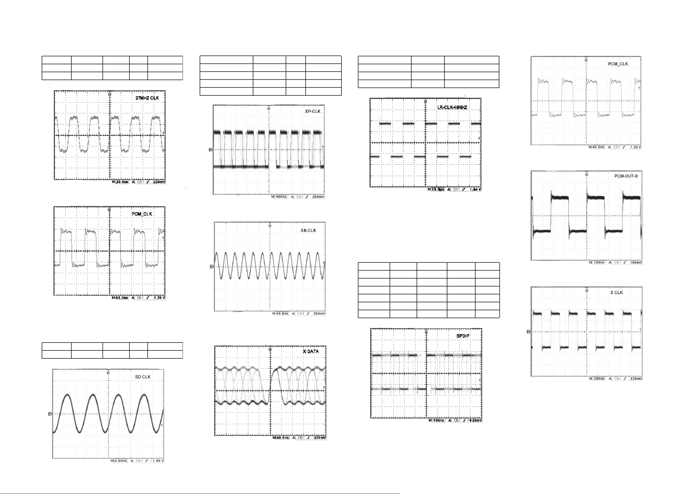
5. DVD Audio Clock 5.1 CH Audio Test Signal
Test name ICS1 pin Test point Condition Figure
SPDIF 47 after RS35 PLAY 5-a
PCM CLK 45 after RS27 PLAY 5-b
PCM-OUT-0 44 after RS28 PLAY 5-c
S CLOCK 43 after RS32 PLAY 5-d
PCM-OUT-1 24 after RS33 PLAY 5-e
PCM-OUT-2 21 after RS34 PLAY 5-f
Figure 5-c
Figure 5-d
Figure 2-a
Figure 5-a
Figure 3-c
2-6
ADDITIONAL INFORMATION FOR DVD SECTION
2-6
Figure 5-e
Figure 5-f
6. Control In / Out
Test name Test point Condition Figure
RXD conn. HS5-RXD FUNCTION PRESS 6-a
TXD conn. HS5-TXD FUNCTION PRESS 6-b
Figure 6-b
7. Video Output Check Playback TDV540 Color Bar
Test name Test point Condition Figure
RED OUT conn. HS6-RED PLAY 7-a
GREEN OUT conn. HS6-GREEN PLAY 7-b
BLUE OUT conn. HS6-BLUE PLAY 7-c
CVBS OUT conn. HS6-CVBS PLAY 7-d
C OUT conn. HS6-C PLAY 7-e
Y OUT conn. HS6-Y PLAY 7-f
Figure 7-c
Figure 7-d
Figure 7-f
8. Tray Open / Close - driver LB1641 output
Test name Test point Value Remarks
SLIDER IN Pin 5 (IC60) 4.3V +/- 2.0V Tray closed
SLIDER OUT Pin 6 (IC60) 3V +/- 1.0V Tray is opening
9. DVD Reset (fig. 9)
400msec. from 0V to 3.3V , if the reset input does not go high then check
the circuit ICS1 pin 29.
Figure 6-a
Figure 7-a
Figure 7-e
Figure 9
Figure 7-b
DISMANTLING INSTRUCTIONS
3-1
3-1
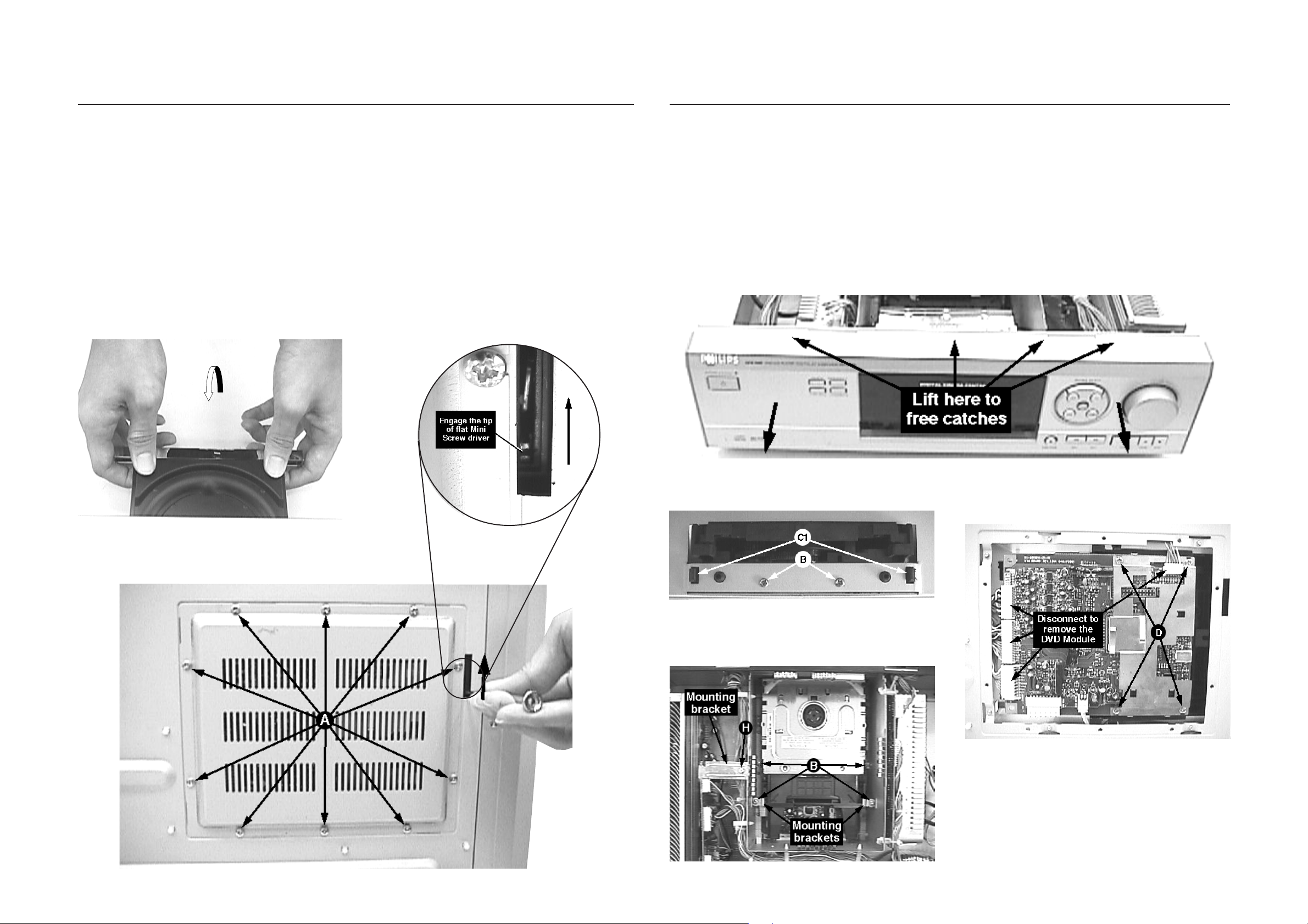
Dismantling of the Front Panel Assembly
1) Open the DVD Tray by using the Open/Close Button while
the Set is ON and disconnect the mains supply after
removing the Tray Cover.
Note: If this is not possible, the DVD T ray has to be open
manually .
To manually open the DVD Tray, place the set on its right
side. Insert a mini flat screw driver into the slot and slide
it upwards as shown in figure 2 until the Tray moves out of
the Front Panel.
2) Return the set to its upright position and remove the Tray
Cover as shown in Figure 1 and close the tray manually by
pushing it back in.
3) Loosen 9 screws and remove the Top Cover by lifting the
rear portion upwards before sliding it out towards the rear.
- 5 screws on the rear
- 2 screws each on the left & right side
4) Loosen 5 screws & lift up the top edge of Front Panel
assembly to free some catches (see figure 3) before
sliding it out towards the front.
- 3 screws on the bottom
- 1 screw each on the left & right side
Dismantling of the DVD Module and/or Digital Board
1) Loosen 10 screws A to remove the DVD Digital Board
cover as shown in figure 2.
Note: Use step 3 to remove the Digital Board without
dismantling the complete DVD Module.
2) Loosen 6 screws B (including 2 metal mounting brackets)
and 2 catches C1 as shown in figure 4 and 5. Disconnect
4 cables (see figure 6) and remove the DVD Module by
lifting its rear end upward and sliding it out of the Front
Metal plate.
Note: - Care should be taken not to entangle / damage
the grounding springs along the DVD enclosure
wall.
- Do not loose the 2 metal mounting brackets.
3) Loosen 4 screws D (see figure 6) and all connectors to
remove the Digital Board.
Figure 1
Figure 3
Figure 4
Figure 6
Figure 2
Figure 5
3-2
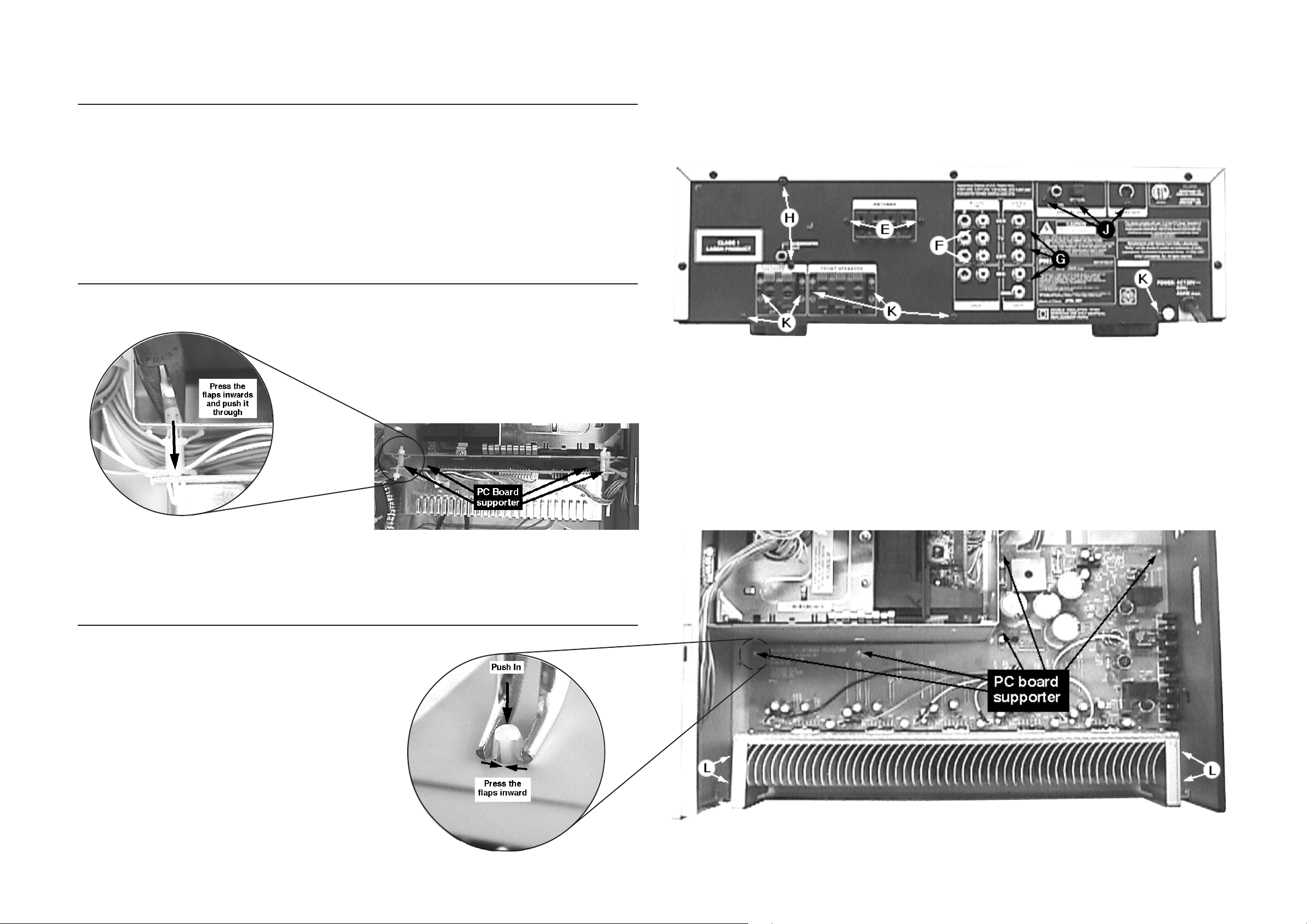
Dismantling the Tuner, Audio Switch, Video Switch, Pro-Logic and AV Board (Refer figure 8)
1) Loosen 2 screws E on the Rear panel to remove the Tuner
Board.
2) Loosen 2 screws F on the Rear panel to remove the Audio
Switch Board.
3) Loosen 3 screws G on the Rear panel to remove the Video
Switch Board.
4) Loosen 3 screws H to remove the Pro-Logic Board.
- 2 screws on the Rear panel
- 1 screw (including metal mounting bracket) on the
inside of the set as shown in figure 5.
5) Loosen 3 screws J on the Rear panel to remove the AV
Output Board.
Dismantling the Regulator Board
1) Release 4 catches of the pc board supporter with a long
nose plier as shown in figure 7.
3-2
Figure 8
Dismantling the Power Amplifier Board
1) With the set upside down, release 5 catches of the pc
board supporter with a long-nose plier as shown in figure
9.
2) With the set upright again, remove the Pro-Logic Board as
describe above.
3) Loosen 4 screws L mounting the heatsink to the bottom
plate as shown in figure 9.
4) Loosen 7 screws K on the Rear Panel (see figure 8)
- 4 screws for the Speaker sockets
- 3 screws to detach the Rear Panel from the bottom
plate.
Figure 7
Figure 9
3-3 3-3
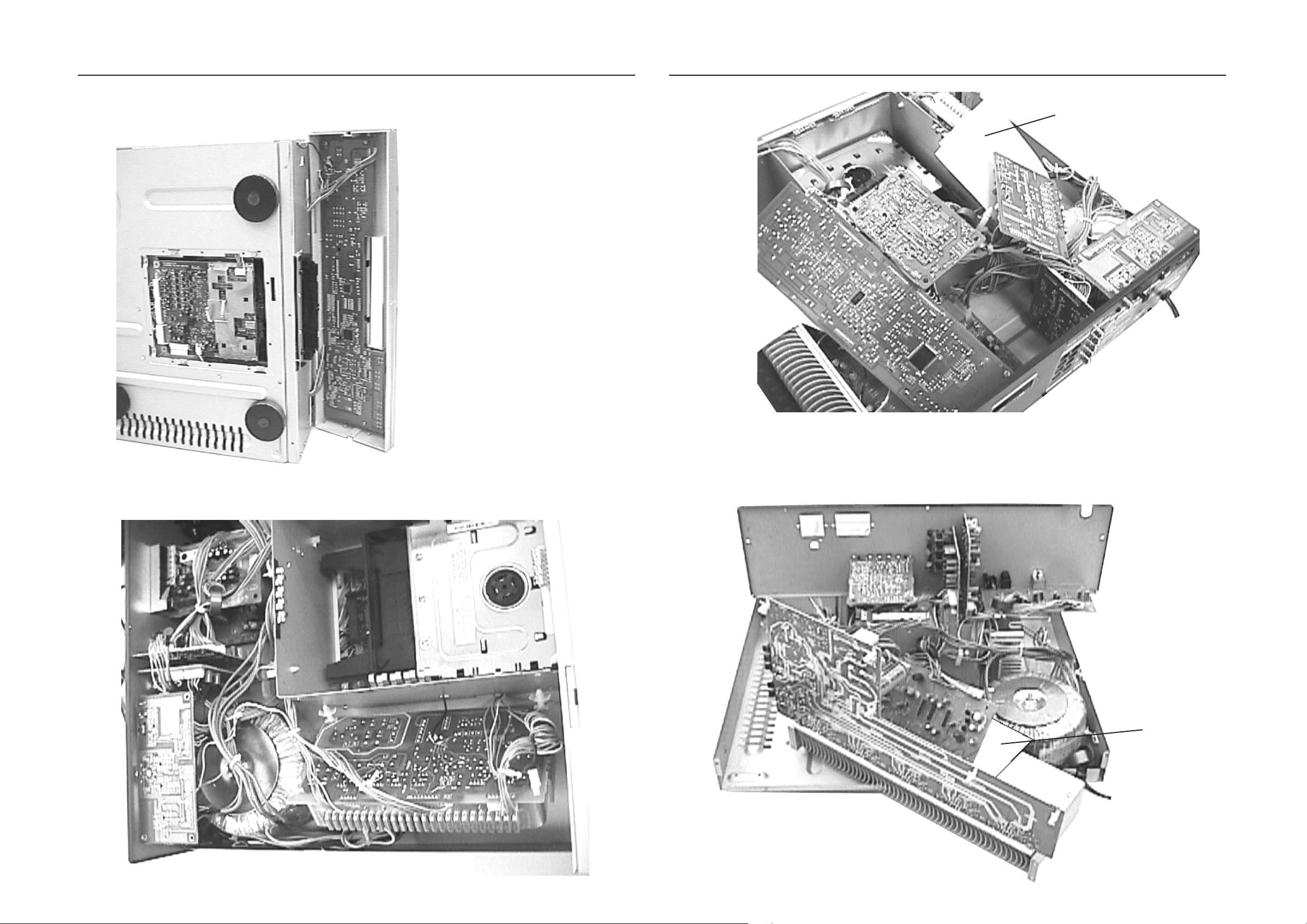
SERVICE POSITIONS & REPAIR HINTS
Service pos A
SERVICE POSITIONS & REPAIR HINTS
Service pos C
Paper
Note: In some service positions the components or copper
patterns of one board may risk touching its neighbouring pc boards or metallic parts. T o prevent such
short-circuit use a piece of hard paper or other
insulating material between them.
Service pos B
Service pos D
Paper
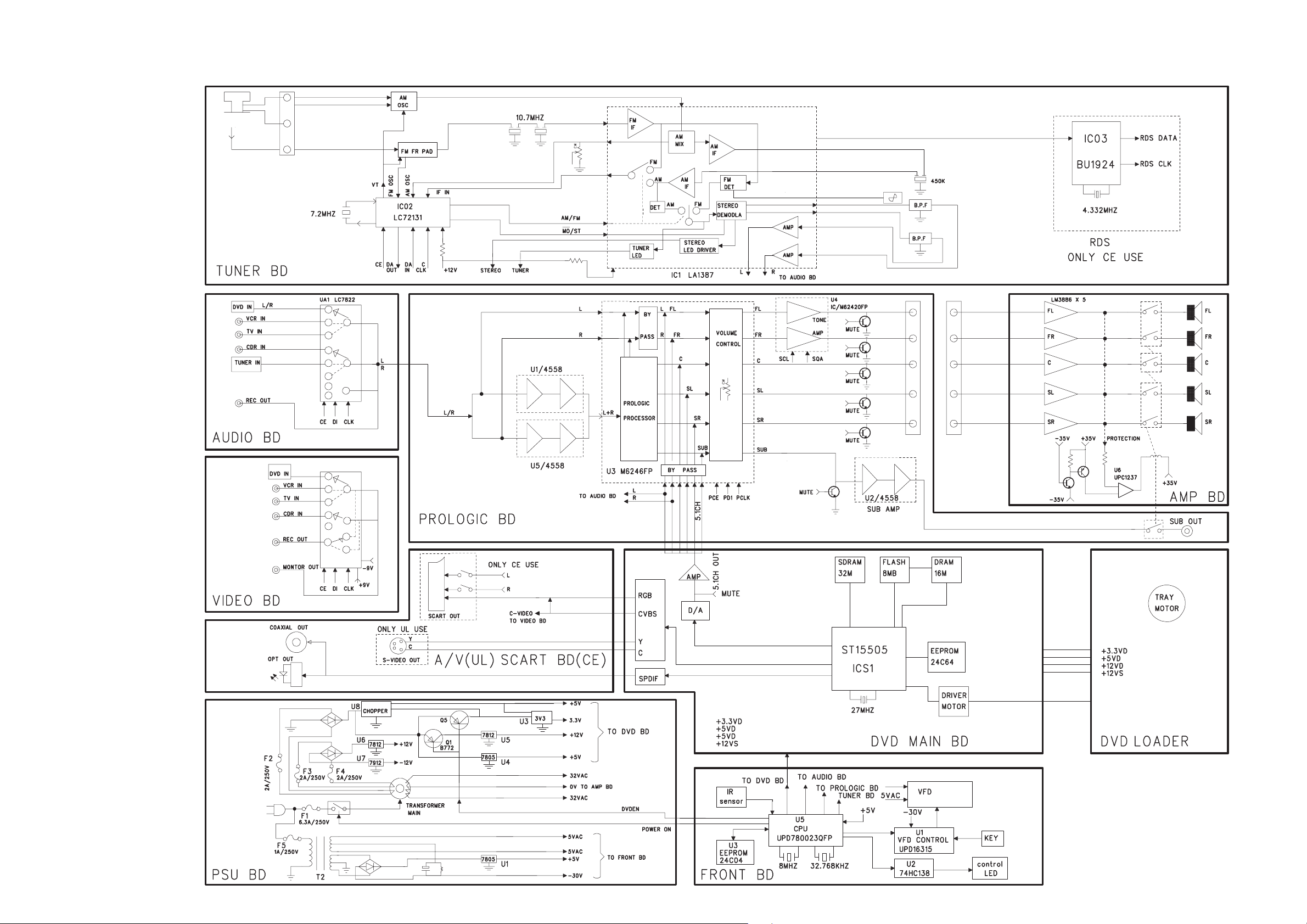
SET BLOCK DIAGRAM
4-1
4-1
MX10... Block Diagram dd wk124-4
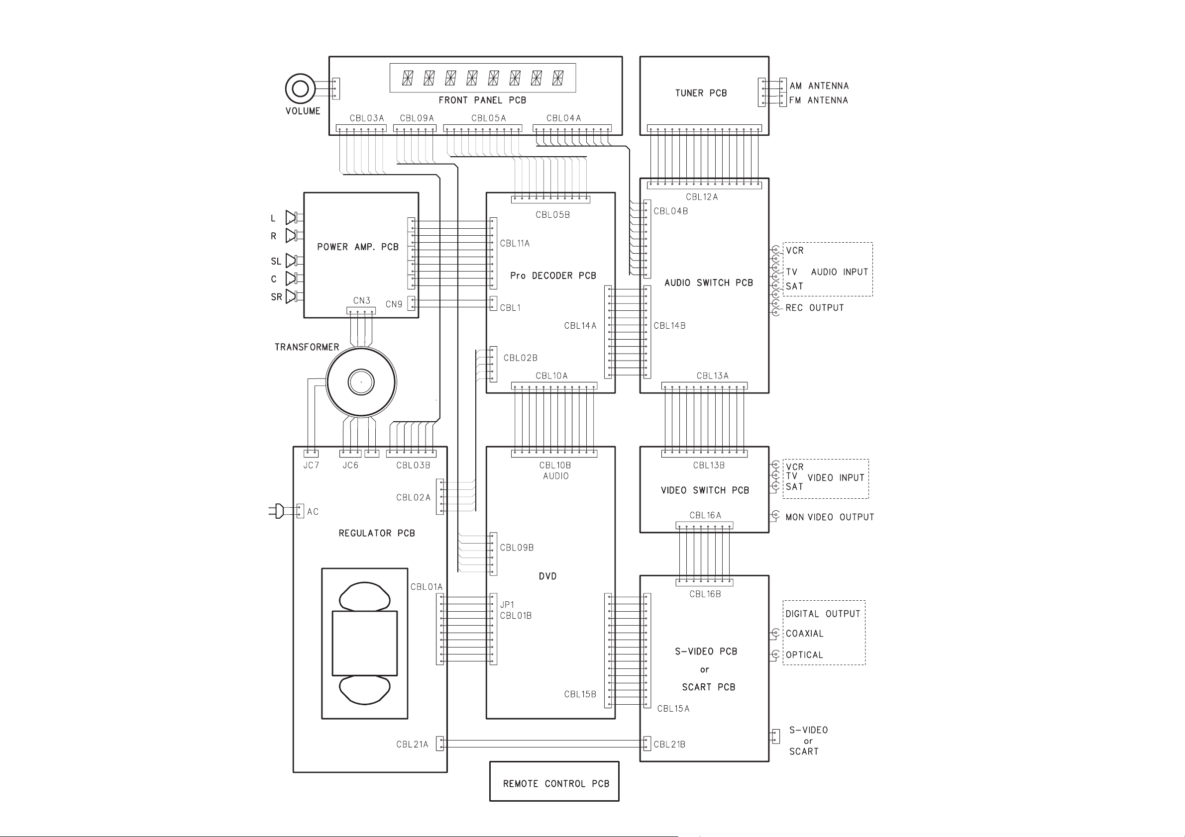
SET WIRING DIAGRAM
4-2 4-2
(PSU BD)
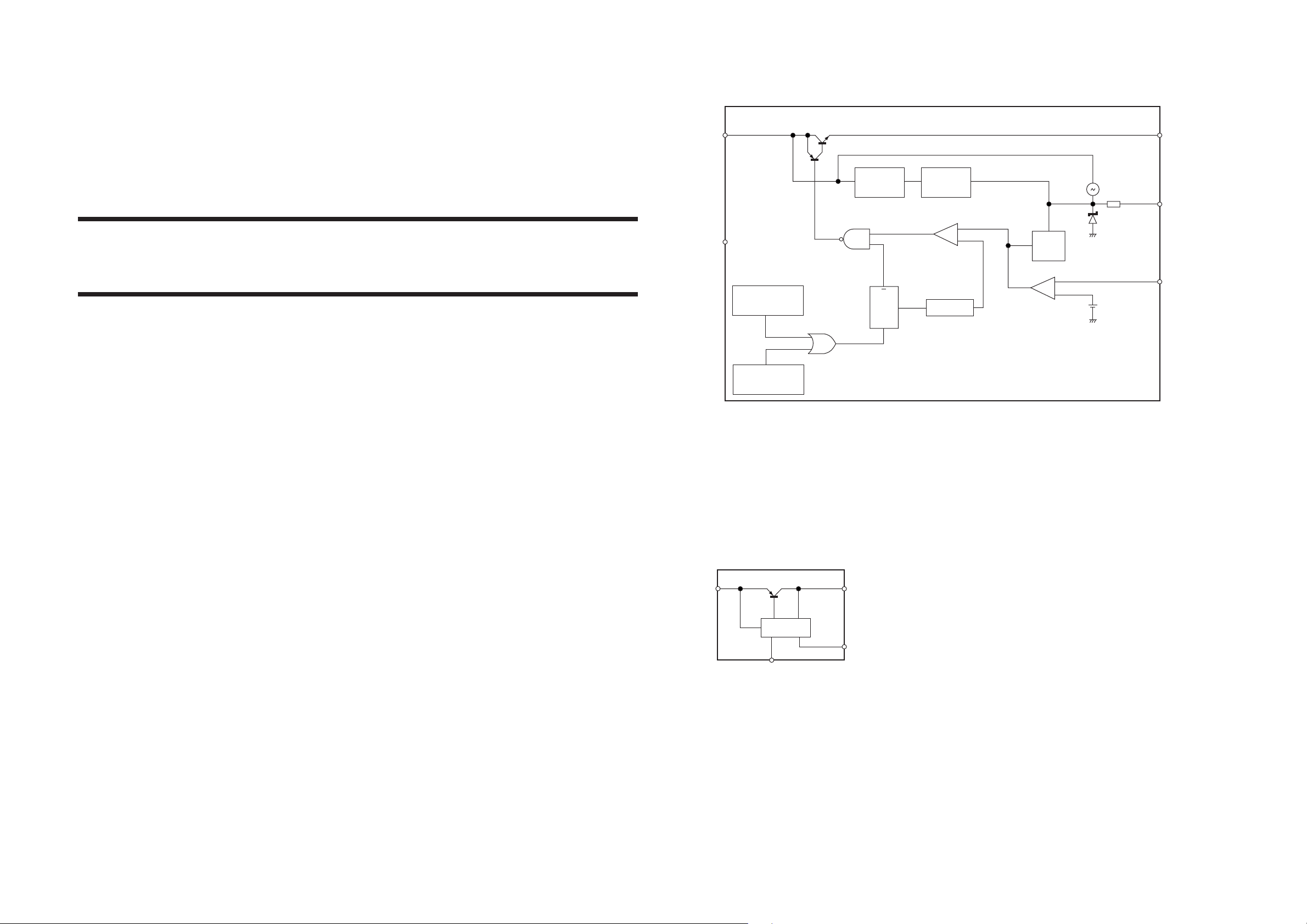
5-1
PQ12CG3032F Internal Block
PQ12CG3032F
V 1
IN
5-1
2 V
OUT
PSU BOARD
TABLE OF CONTENTS
PQ12CG3032F & PQ3RD13 Internal Block.................... 5-1
Components Layout + Voltages ...................................... 5-2
Circuit Diagram ................................................................ 5-3
Electrical parts list............................................................ 5-4
COM 3
Overcurrent
Detection Cricuit
Overheat
Detection Circuit
Voltage
Regulator
Q
F/F
S
PWM Comp
R
On/Off
Circuit
+
-
Oscillator
Soft
Start
-
+
Error Amp.
Vref
5 ON/OFF
4 0
ADJ
PQ3RD13 Internal Block
DC Input 1
Specific IC
3 GND
2 DC Output
4 ON/OFF Control
 Loading...