


查询Z0103供应商
1. Product profile
1.1 Description
Z0103/07/09 series
Triacs
Rev. 02 — 12 September 2002 Product data
Passivatedtriacs in conventional and surfacemounting packages. Intended for use in
applications requiring high bidirectional transient and blocking voltage capability.
Available in a range of gate current sensitivities for optimum performance.
Product availability:
Z0103MA; Z0103NA; Z0107MA; Z0107NA; Z0109MA; Z0109NA in SOT54B
Z0103MN; Z0103NN; Z0107MN; Z0107NN; Z0109MN; Z0109NN in SOT223.
1.2 Features
■ Blocking voltage to 800 V (NA and NN
types)
■ 1 A on-state RMS current.
1.3 Applications
■ Home appliances ■ Small motor control
■ Fan controllers ■ Small loads in industrial process
control.
2. Pinning information
Table 1: Pinning - SOT54B (TO-92), SOT223, simplified outline and symbol
Pin Description Simplified outline Symbol
1 terminal 2 (T2) SOT54B
2 gate (G)
3 terminal 1 (T1)
1 terminal 1 (T1) SOT223
2 terminal 2 (T2)
3 gate (G)
4 terminal 2 (T2)
(TO-92)
1
2
3
MSB033
123
Top view
4
MSB002 - 1
T2
T1
G
MBL300
SOT54B (TO-92)
SOT223

Philips Semiconductors
Z0103/07/09 series
3. Ordering information
3.1 Ordering options
Table 2: Ordering information
Part Number Voltage (V
Z0103MA 600 V 3 mA SOT54B (TO-92)
Z0103NA 800 V 3 mA SOT54B (TO-92)
Z0107MA 600 V 5 mA SOT54B (TO-92)
Z0107NA 800 V 5 mA SOT54B (TO-92)
Z0109MA 600 V 10 mA SOT54B (TO-92)
Z0109NA 800 V 10 mA SOT54B (TO-92)
Z0103MN 600 V 3 mA SOT223
Z0103NN 800 V 3 mA SOT223
Z0107MN 600 V 5 mA SOT223
Z0107NN 800 V 5 mA SOT223
Z0109MN 600 V 10 mA SOT223
Z0109NN 800 V 10 mA SOT223
) Gate Sensitivity (IGT) Package
DRM
Triacs
4. Limiting values
Table 3: Limiting values
In accordance with the Absolute Maximum Rating System (IEC 60134).
Symbol Parameter Conditions Min Max Unit
V
DRM
V
RRM
I
TSM
I
T(RMS)
2
tI
I
dI
T
I
GM
P
GM
P
G(AV)
T
stg
T
j
9397 750 10102
Product data Rev. 02 — 12 September 2002 2 of 12
repetitive peak off-state voltage 25 °C ≤ Tj≤ 125 °C
Z0103/07/09MA; Z0103/07/09MN - 600 V
Z0103/07/09NA; Z0103/07/09NN - 800 V
repetitive peak reverse voltage 25 °C ≤ Tj≤ 125 °C
Z0103/07/09MA; Z0103/07/09MN - 600 V
Z0103/07/09NA; Z0103/07/09NN - 800 V
non-repetitive peak on-state current full sine wave; Tj= 25 °C prior to surge;
Figure 2 and Figure 3
t=20ms - 8 A
t = 16.7 ms - 8.5 A
RMS on-state current all conduction angles; Figure 4
SOT223 T
SOT54B (TO-92) T
2
t for fusing t = 10 ms - 0.35 A2s
=90°C-1A
sp
=50°C-1A
lead
/dt rate of rise of on-state current ITM= 1.0 A; IG=2xIGT; dIG/dt = 100 mA/µs - 20 A/µs
peak gate current tp=20µs - 1.0 A
peak gate power - 2.0 W
average gate power over any 20 ms period - 0.1 W
storage temperature −40 +150 °C
junction temperature −40 +125 °C
© Koninklijke Philips Electronics N.V. 2002. All rights reserved.
Philips Semiconductors
Z0103/07/09 series
Triacs
P
tot
(W)
1.6
1.2
0.8
0.4
003aaa199
I
T(RMS)
α =
180°
120°
90°
60°
30°
1.20 0.4 0.8
(A)
α
α
0
I
TSM
(A)
10
8
6
4
2
0
1
10
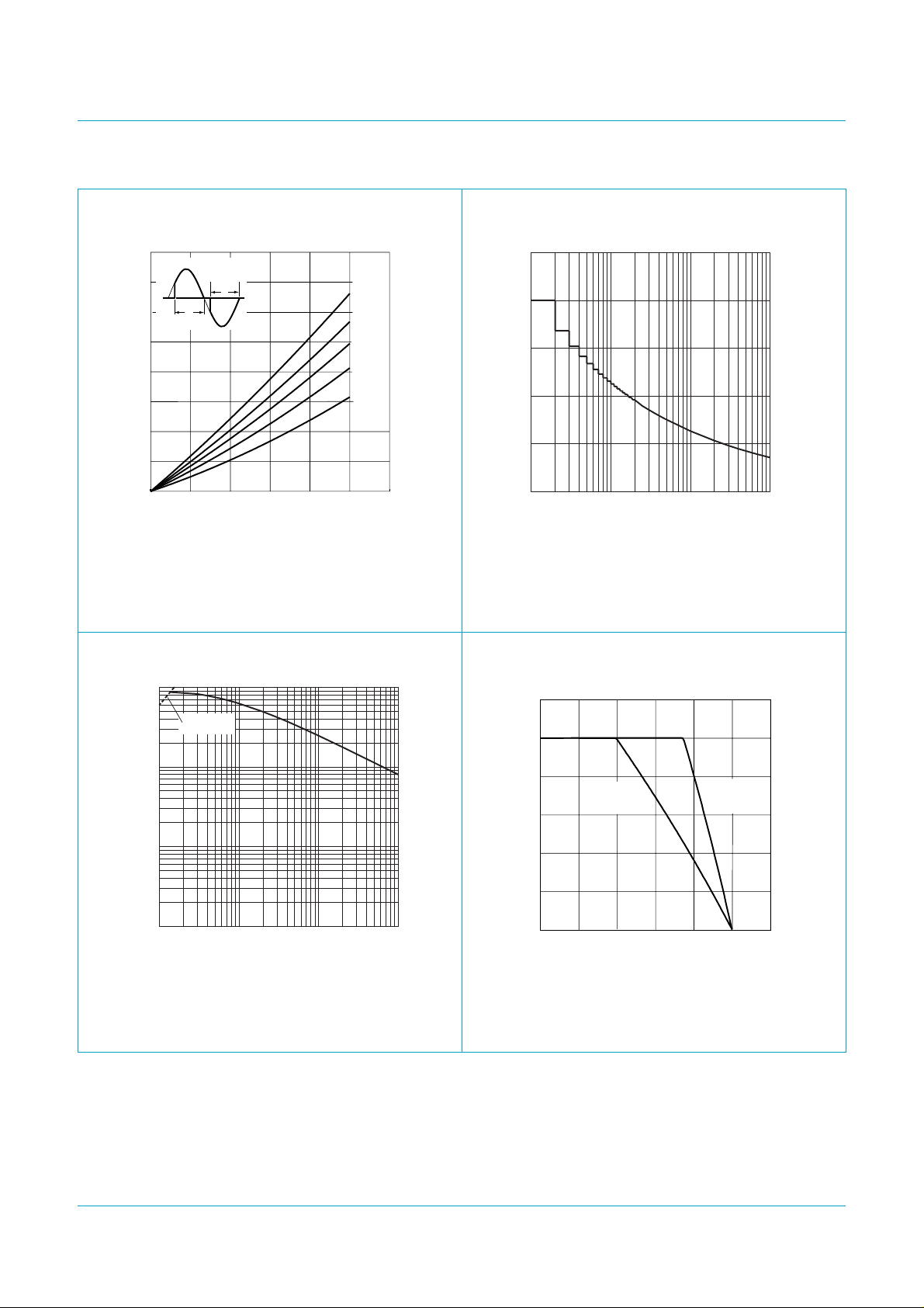
α = conduction angle n = number of cycles at f = 50 Hz
Fig 1. Maximum on-state power dissipation as a
function of RMS on-state current; typical
values.
003aaa207
I
TSM
(A)
2
10
δIT/δt limit
10
Fig 2. Maximum permissible non-repetitive peak
on-state current as a function of number of
cycles for sinusoidal currents; typical values.
1.2
I
T(RMS)
(A)
0.8
SOT54B
(T
lead
003aaa200
2
10
SOT223
)
(Tsp)
n
003aaa201
3
10
1
-1
10
-5
10
-4
10
-3
10
ts (s)
Fig 3. Maximum permissible non-repetitive peak
on-state current as a function of surge duration
for sinusoidal currents; typical values.
9397 750 10102
-2
10
Fig 4. Maximum permissible RMS on-state current as
0.4
0
50
1000
T
lead, Tsp
150
(°C)
a function of lead temperature and solder point
temperature; typical values.
© Koninklijke Philips Electronics N.V. 2002. All rights reserved.
Product data Rev. 02 — 12 September 2002 3 of 12
Philips Semiconductors
Z0103/07/09 series
Triacs
5. Thermal characteristics
Table 4: Thermal characteristics
Symbol Parameter Conditions Min Typ Max Unit
R
th(j-sp)
R
th(j-lead)
R
th(j-a)
thermal resistance from junction to solder
Figure 5
point for SOT223
thermal resistance from junction to lead for
Figure 5
SOT54B (TO-92)
thermal resistance from junction to ambient
SOT223 minimum footprint; mounted on a PCB - 60 - K/W
SOT54B (TO-92) vertical in free air - 150 - K/W
5.1 Transient thermal impedance
--25K/W
--60K/W
10
a
1
-1
10
-2
10
-3
10
-4
10
10
Z
th j lead–()
=
a
---------------------------
R
th j lead–()
Z
th j sp–()
a
=
---------------------- -
R
th j sp–()
-5
SOT223
-4
10
for SOT54B (TO-92)
for SOT223
SOT54B
-3
10
-2
10
-1
10
11010
003aaa206
2
tp (s)
3
10
Fig 5. Transient thermal impedance from junction to lead and junction to solder point as a function of pulse
duration.
9397 750 10102
© Koninklijke Philips Electronics N.V. 2002. All rights reserved.
Product data Rev. 02 — 12 September 2002 4 of 12

Philips Semiconductors
Z0103/07/09 series
Triacs
6. Characteristics
Table 5: Characteristics
Tj=25°C unless otherwise specified.
Symbol Parameter Conditions Min Typ Max Unit
Static characteristics
I
GT
I
L
I
H
V
T
V
GT
I
D
Dynamic characteristics
dV
D
dV
com
gate trigger current VD=12V; RL=30Ω; T2+ G+; T2+ G−; T2− G−;
Z0103MA/MN/NA/NN - - 3 mA
Figure 9
Z0107MA/MN/NA/NN - - 5 mA
Z0109MA/MN/NA/NN - - 10 mA
Z0103MA/MN/NA/NN
VD= 12 V; RL=30Ω; T2− G+; Figure 9
--5mA
Z0107MA/MN/NA/NN - - 7 mA
Z0109MA/MN/NA/NN - - 10 mA
latching current VD=12V; RL=30Ω; T2+ G+; T2− G−; T2− G+;
Z0103MA/MN/NA/NN - - 7 mA
Figure 7
Z0107MA/MN/NA/NN - - 10 mA
Z0109MA/MN/NA/NN - - 15 mA
Z0103MA/MN/NA/NN V
=12V; RL=30Ω; T2+ G−; Figure 7 --15mA
D
Z0107MA/MN/NA/NN - - 20 mA
Z0109MA/MN/NA/NN - - 25 mA
holding current IT=50mA;Figure 8
Z0103MA/MN/NA/NN - - 7 mA
Z0107MA/MN/NA/NN - - 10 mA
Z0109MA/MN/NA/NN - - 10 mA
on-state voltage Figure 6 - 1.3 1.6 V
gate trigger voltage VD=12V; RL=30Ω; Tj=25°C; Figure 11 - - 1.3 V
; RL= 3.3 kΩ; Tj= 125 °C; Figure 11 0.2 - - V
DRM(max)
DRM(max)
; VR=V
RRM(max); Tj
; Tj= 110 °C; exponential
= 125 °C - - 500 µA
off-state leakage current VD=V
/dt critical rate of rise of
off-state voltage
V
D=VDRM
VD= 0.67 V
waveform; gate open; Figure 10
Z0103MA/MN/NA/NN 10 - - V/µs
Z0107MA/MN/NA/NN 20 - - V/µs
Z0109MA/MN/NA/NN 50 - - V/µs
/dt critical rate of change of
commutating voltage
VD= 400 V; IT= 1 A; Tj= 110 °C;
/dt = 0.44 A/ms; gate open
dI
com
Z0103MA/MN/NA/NN 0.5 - - V/µs
Z0107MA/MN/NA/NN 1 - - V/µs
Z0109MA/MN/NA/NN 2 - - V/µs
9397 750 10102
Product data Rev. 02 — 12 September 2002 5 of 12
© Koninklijke Philips Electronics N.V. 2002. All rights reserved.

Philips Semiconductors
Z0103/07/09 series
Triacs
8
I
T
(A)
6
4
2
0
0123
125 °C
max
125 °C
typ
003aaa202
25 °C
max
VT (V)
Fig 6. On-state current as a function of on-state
voltage; typical and maximum values.
3
a
2
1
0
-50 0 50 100 150
I
L
=
a
------------------ -
I
°
L25C
()
003aaa203
Tj (°C)
Fig 7. Normalized latching current as a function of
junction temperature; typical values.
3
a
2
1
0
-50 0 50 100 150
I
H
= a
a
------------------- -
I
°
H25C
()
003aaa204
Tj (°C)
Fig 8. Normalized holding current as a function of
junction temperature; typical values.
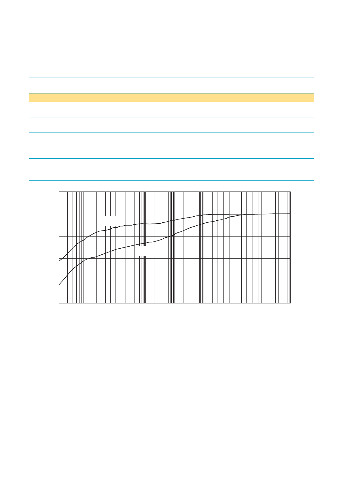
4
a
3
2
1
0
=
0 50 100 150-50
I
GT
---------------------- -
I
GT 25 C°()
T2+ G+
T2+ GT2- G+
T2- G-
003aaa205
Tj (°C)
Fig 9. Normalized gate trigger current as a function of
junction temperature; typical values.
9397 750 10102
© Koninklijke Philips Electronics N.V. 2002. All rights reserved.
Product data Rev. 02 — 12 September 2002 6 of 12

Philips Semiconductors
Z0103/07/09 series
Triacs
1.6
a
1.2
0.8
0.4
0
0
=
a
---------------------------------- -
dV
dt⁄
dV
D
D25°C()
dt⁄
50
003aaa208
100 150
Tj (
°
C)
Fig 10. Normalized critical rate of rise of off-state
voltage as a function of junction temperature;
typical values.
1.6
a
1.2
0.8
0.4
0
V
=
------------------------ -
V
GT 25 C°()
GT
a
003aaa209
150100500-50
Tj (°C)
Fig 11. Normalized gate trigger voltage as a function of
junction temperature; typical values.
9397 750 10102
© Koninklijke Philips Electronics N.V. 2002. All rights reserved.
Product data Rev. 02 — 12 September 2002 7 of 12

Philips Semiconductors
Z0103/07/09 series
7. Package outline
Plastic single-ended leaded (through hole) package; 3 leads SOT54B
c
E
d
A L
b
Triacs
1
D
2
3
b
1
0 2.5 5 mm
scale
DIMENSIONS (mm are the original dimensions)
b
UNIT
A
4.8
4.4
0.45
0.36
mm
Note
1. Terminal dimensions within this zone are uncontrolled to allow for flow of plastic and terminal irregularities.
OUTLINE
VERSION
SOT54B TO-92
1
b
max
0.48
c
D
d
E
e
0.43
4.7
1.7
3.7
0.33
4.5
1.4
REFERENCES
IEC JEDEC JEITA
3.4
2.54
e
1.27
L
1
(1)
L
L
15.2
12.7
1
1.55
1.45
1
EUROPEAN
PROJECTION
e
1
e
ISSUE DATE
02-01-29
Fig 12. SOT54B (TO-92).
9397 750 10102
Product data Rev. 02 — 12 September 2002 8 of 12
© Koninklijke Philips Electronics N.V. 2002. All rights reserved.

Philips Semiconductors
Z0103/07/09 series
Plastic surface mounted package; collector pad for good heat transfer; 4 leads SOT223
Triacs
D
y
b
1
132
e
1
e
E
c
H
E
AB
X
v M
A
4
Q
A
A
1
L
p
b
p
w M
B
detail X
0 2 4 mm
scale
DIMENSIONS (mm are the original dimensions)
UNIT A1b
A
0.10
1.8
mm
OUTLINE
VERSION
SOT223 SC-73
1.5
0.01
p
0.80
0.60
IEC JEDEC EIAJ
3.1
2.9
b
1
cD
0.32
6.7
0.22
6.3
e
E
3.7
4.6
3.3
REFERENCES
e1HELpQywv
7.3
1.1
2.3
6.7
0.7
0.95
0.85
0.1 0.10.2
EUROPEAN
PROJECTION
ISSUE DATE
97-02-28
99-09-13
Fig 13. SOT223.
9397 750 10102
Product data Rev. 02 — 12 September 2002 9 of 12
© Koninklijke Philips Electronics N.V. 2002. All rights reserved.

Philips Semiconductors
8. Revision history
Table 6: Revision history
Rev Date CPCN Description
02 20020912 Product data; supersedes data of 11 April 2002
Table 5 “Characteristics” Addition of dV
01 20020411 - Product data; initial version (9397 750 09419)
/dt data. Correction to dVD/dt data
com
Z0103/07/09 series
Triacs
9397 750 10102
Product data Rev. 02 — 12 September 2002 10 of 12
© Koninklijke Philips Electronics N.V. 2002. All rights reserved.

Philips Semiconductors
Philips Semiconductors
9. Data sheet status
Z0103/07/09 series
Z0103/07/09 series
Triacs
Triacs
Data sheet status
Objective data Development This data sheetcontains data from the objectivespecificationfor product development.Philips Semiconductors
Preliminary data Qualification This data sheet contains data from the preliminary specification. Supplementary data will be published at a
Product data Production This data sheet contains data from the product specification. Philips Semiconductors reserves the right to
[1] Please consult the most recently issued data sheet before initiating or completing a design.
[2] The product status of the device(s) described in this data sheet may have changed since this data sheet was published. The latest information is available on the Internet at
URL http://www.semiconductors.philips.com.
[1]
Product status
10. Definitions
Short-form specification — The data in a short-form specification is
extracted from a full data sheet with the same type number and title. For
detailed information see the relevant data sheet or data handbook.
Limiting values definition — Limiting values given are in accordance with
the Absolute Maximum Rating System (IEC 60134). Stress above one or
more of the limiting values may cause permanent damage to the device.
These are stress ratings only and operation of the device at these or at any
other conditions above those given in the Characteristics sections of the
specification is not implied. Exposure to limiting values for extended periods
may affect device reliability.
Application information — Applications that are described herein for any
of these products are for illustrative purposes only. Philips Semiconductors
make no representation or warranty that such applications will be suitable for
the specified use without further testing or modification.
[2]
Definition
reserves the right to change the specification in any manner without notice.
later date. Philips Semiconductors reserves the right to change the specification without notice, in order to
improve the design and supply the best possible product.
make changes at any time in order to improve the design, manufacturing and supply. Changes will be
communicated according to the Customer Product/Process Change Notification (CPCN) procedure
SNW-SQ-650A.
11. Disclaimers
Life support — These products are not designed for use in life support
appliances, devices, or systems where malfunction of these products can
reasonably be expected to result in personal injury. Philips Semiconductors
customers using or selling these products for use in such applications do so
at their own risk and agree to fully indemnify Philips Semiconductors for any
damages resulting from such application.
Right to make changes — Philips Semiconductors reserves the right to
make changes, without notice, in the products, including circuits, standard
cells, and/or software, described or contained herein in order to improve
design and/or performance. Philips Semiconductors assumes no
responsibility or liability for the use of any of these products, conveys no
licence or title under any patent, copyright, or mask work right to these
products, andmakes no representations orwarrantiesthat these productsare
free from patent,copyright,or mask work right infringement, unless otherwise
specified.
Contact information
For additional information, please visit http://www.semiconductors.philips.com.
For sales office addresses, send e-mail to: sales.addresses@www.semiconductors.philips.com. Fax: +31 40 27 24825
© Koninklijke Philips Electronics N.V. 2002. All rights reserved.
9397 750 10102
9397 750 10102
Product data Rev. 02 — 12 September 2002 11 of 12
Product data Rev. 02 — 12 September 2002 11 of 12
© Koninklijke Philips Electronics N.V. 2002. All rights reserved.

Philips Semiconductors
Contents
1 Product profile . . . . . . . . . . . . . . . . . . . . . . . . . . 1
1.1 Description . . . . . . . . . . . . . . . . . . . . . . . . . . . . 1
1.2 Features . . . . . . . . . . . . . . . . . . . . . . . . . . . . . . 1
1.3 Applications . . . . . . . . . . . . . . . . . . . . . . . . . . . 1
2 Pinning information. . . . . . . . . . . . . . . . . . . . . . 1
3 Ordering information. . . . . . . . . . . . . . . . . . . . . 2
3.1 Ordering options. . . . . . . . . . . . . . . . . . . . . . . . 2
4 Limiting values. . . . . . . . . . . . . . . . . . . . . . . . . . 2
5 Thermal characteristics. . . . . . . . . . . . . . . . . . . 4
5.1 Transient thermal impedance . . . . . . . . . . . . . . 4
6 Characteristics. . . . . . . . . . . . . . . . . . . . . . . . . . 5
7 Package outline . . . . . . . . . . . . . . . . . . . . . . . . . 8
8 Revision history. . . . . . . . . . . . . . . . . . . . . . . . 10
9 Data sheet status. . . . . . . . . . . . . . . . . . . . . . . 11
10 Definitions . . . . . . . . . . . . . . . . . . . . . . . . . . . . 11
11 Disclaimers. . . . . . . . . . . . . . . . . . . . . . . . . . . . 11
Z0103/07/09 series
Triacs
© Koninklijke Philips Electronics N.V. 2002.
Printed in The Netherlands
All rights are reserved. Reproduction in whole or in part is prohibited without the prior
written consent of the copyright owner.
The information presented in this document does not form part of any quotation or
contract, is believed to be accurate and reliable and may be changed without notice. No
liability will be accepted by the publisher for any consequence of its use. Publication
thereof does not convey nor imply any license under patent- or other industrial or
intellectual property rights.
Date of release: 12 September 2002 Document order number: 9397 750 10102
 Loading...