Philips xr2206 DATASHEETS
...the analog plus company
FEA TURES
Low-Sine Wave Distortion, 0.5%, Typical
Excellent Temperature Stability, 20ppm/°C, Typ.
Wide Sweep Range, 2000:1, Typical
Low-Supply Sensitivity , 0.01%V, T yp.
Linear Amplitude Modulation
TTL Compatible FSK Controls
Wide Supply Range, 10V to 26V
Adjustable Duty Cycle, 1% TO 99%
GENERAL DESCRIPTION
TM
APPLICATIONS
Waveform Generation
Sweep Generation
AM/FM Generation
V/F Conversion
FSK Generation
Phase-Locked Loops (VCO)
Function Generator
XR-2206
Monolithic
June 1997-3
The XR-2206 is a monolithic function generator
integrated circuit capable of producing high quality sine,
square, triangle, ramp, and pulse waveforms of
high-stability and accuracy . The output waveforms can be
both amplitude and frequency modulated by an external
voltage. Frequency of operation can be selected
externally over a range of 0.01Hz to more than 1MHz.
ORDERING INFORMA TION
Part No. Package
XR-2206M 16 Lead 300 Mil CDIP
XR-2206P 16 Lead 300 Mil PDIP
XR-2206CP 16 Lead 300 Mil PDIP
XR-2206D 16 Lead 300 Mil JEDEC SOIC
The circuit is ideally suited for communications,
instrumentation, and function generator applications
requiring sinusoidal tone, AM, FM, or FSK generation. It
has a typical drift specification of 20ppm/°C. The oscillator
frequency can be linearly swept over a 2000:1 frequency
range with an external control voltage, while maintaining
low distortion.
Operating
T emperature Range
-55°C to +125°C
–40°C to +85°C
0°C to +70°C
0°C to +70°C
Rev. 1.03
1972
EXAR Corporation, 48720 Kato Road, Fremont, CA 94538 (510) 668-7000 (510) 668-7017
1
XR-2206
Timing
Capacitor
Timing
Resistors
FSKI
TC1
TC2
TR1
TR2
GND10BIAS
V
CC
12
4
5
VCO
6
7
Current
8
9
Switches
Multiplier
And Sine
Shaper
+1
11 SYNCO
2
STO
AMSI
1
13WAVEA1
14WAVEA2
15SYMA1
16SYMA2
3MO
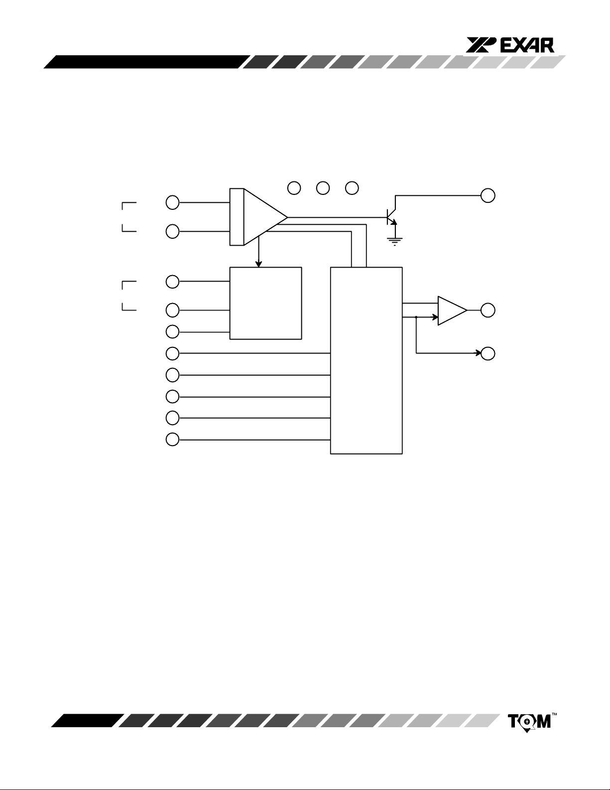
Figure 1. XR-2206 Block Diagram
Rev. 1.03
2
XR-2206
STO
MO
V
CC
TC1
TC2
TR1
TR2
1
2
3
4
5
6
7
8
AMSI
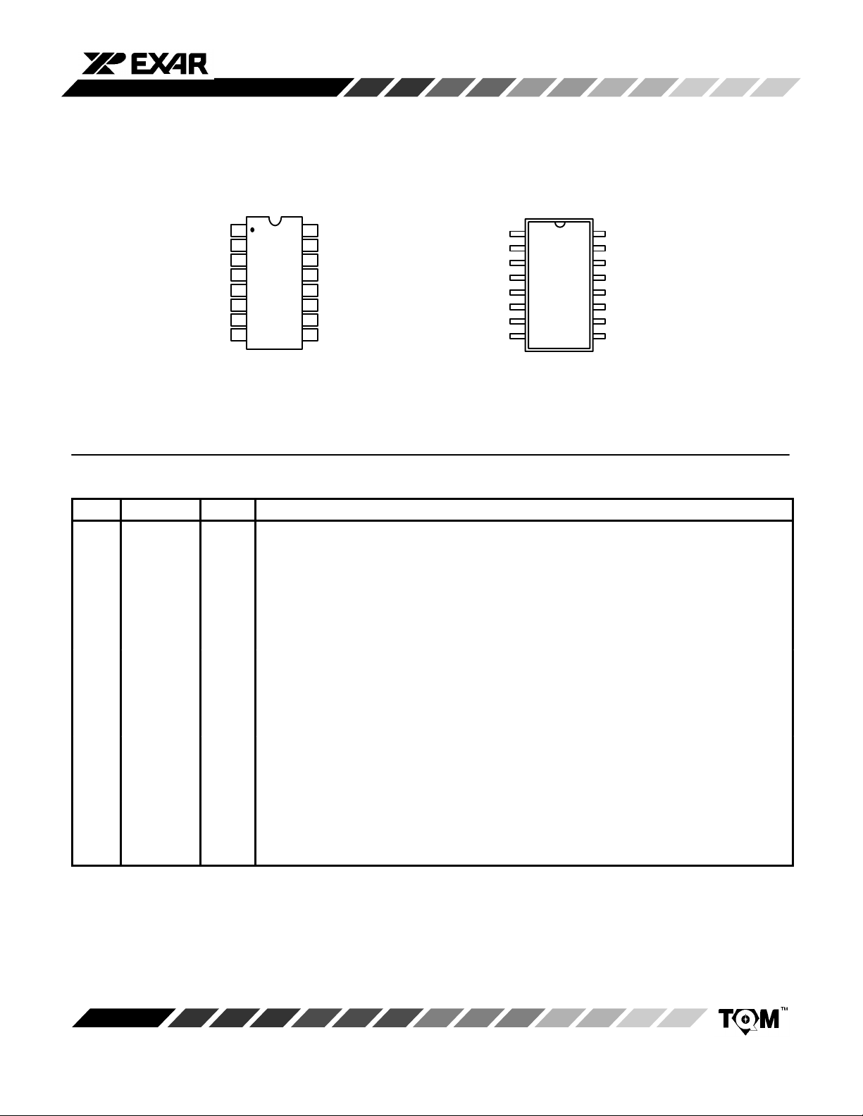
16 Lead PDIP, CDIP (0.300”)
16
15
14
13
12
11
10
9
SYMA2
SYMA1
WAVEA2
WAVEA1
GND
SYNCO
BIAS
FSKI
161
AMSI
STO
MO
V
CC
TC1
TC2
TR1
TR2
2
3
4
5
6
7
SYMA2
15
SYMA1
14
WAVEA2
13
WAVEA1
GND
12
11
SYNCO
10
BIAS
98
FSKI
16 Lead SOIC (Jedec, 0.300”)
PIN DESCRIPTION
Pin # Symbol Type Description
1 AMSI I Amplitude Modulating Signal Input.
2 STO O Sine or Triangle Wave Output.
3 MO O Multiplier Output.
4 V
CC
5 TC1 I Timing Capacitor Input.
6 TC2 I Timing Capacitor Input.
7 TR1 O Timing Resistor 1 Output.
8 TR2 O Timing Resistor 2 Output.
9 FSKI I Frequency Shift Keying Input.
10 BIAS O Internal Voltage Reference.
11 SYNCO O Sync Output. This output is a open collector and needs a pull up resistor to VCC.
12 GND Ground pin.
13 WAVEA1 I Wave Form Adjust Input 1.
14 WAVEA2 I Wave Form Adjust Input 2.
15 SYMA1 I Wave Symetry Adjust 1.
16 SYMA2 I Wave Symetry Adjust 2.
Positive Power Supply .
Rev. 1.03
3
XR-2206
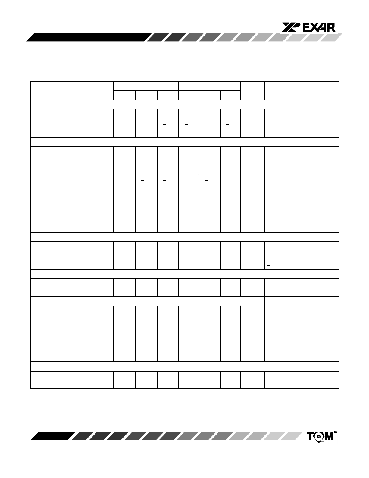
DC ELECTRICAL CHARACTERISTICS
Test Conditions: Test Circuit of
Unless Otherwise Specified. S
Parameters Min. T yp. Max. Min. Typ. Max. Units Conditions
General Characteristics
Single Supply Voltage 10 26 10 26 V
Split-Supply Voltage
Supply Current 12 17 14 20 mA
Oscillator Section
Max. Operating Frequency 0.5 1 0.5 1 MHz
Lowest Practical Frequency 0.01 0.01 Hz
Frequency Accuracy +1 +4 +2 % of fofo = 1/R1C
Temperature Stability
Frequency
Sine Wave Amplitude Stability
Supply Sensitivity 0.01 0.1 0.01 %/V V
Sweep Range 1000:1 2000:1 2000:1 fH = f
Sweep Linearity
10:1 Sweep 2 2 % fL = 1kHz, f
1000:1 Sweep 8 8 % f
FM Distortion 0.1 0.1 % +10% Deviation
Recommended Timing Components
Timing Capacitor: C 0.001 100 0.001 100
Timing Resistors: R1 & R
Triangle Sine Wave Output
Triangle Amplitude 160 160
Sine Wave Amplitude 40 60 80 60
Max. Output Swing 6 6 Vp-p
Output Impedance 600 600
Triangle Linearity 1 1 %
Amplitude Stability 0.5 0.5 dB For 1000:1 Sweep
Sine Wave Distortion
Without Adjustment 2.5 2.5 %
With Adjustment 0.4 1.0 0.5 1.5 % See
2
Figure 2
open for triangle, closed for sine wave.
1
Vcc = 12V, TA = 25°C, C = 0.01F, R
XR-2206M/P XR-2206CP/D
+5
+13 +5 +13 V
+10 +50 +20
2
4800 4800
1 2000 1 2000
1
= 100k, R2 = 10k, R3 = 25k
1
R
10k
1
C = 1000pF, R1 = 1k
C = 50F, R
ppm/°C 0°C T
R
= R2 = 20k
1
1
70°C
A
= 2M
ppm/°C
= 10V, V
LOW
= R
= 20k
1
2
@ R1 = 2M
= 10kHz
H
= 100Hz, fH = 100kHz
L
F
R
fH @ R1 = 1k
f
L
L
Figure 5
k
Figure 3
mV/k
mV/k
Figure 2,
Figure 2
S1 Open
, S1 Closed
R1 = 30k
Figure 7
and
HIGH
Figure 8
= 20V,
Notes
1
Output amplitude is directly proportional to the resistance, R3, on Pin 3. See Figure 3.
2
For maximum amplitude stability , R3 should be a positive temperature coefficient resistor.
Bold face parameters are covered by production test and guaranteed over operating temperature range.
Rev. 1.03
4
XR-2206
DC ELECTRICAL CHARACTERISTICS (CONT’D)
XR-2206M/P XR-2206CP/D
Parameters Min. Typ. Max. Min. Typ. Max. Units Conditions
Amplitude Modulation
Input Impedance 50 100 50 100
Modulation Range 100 100 %
Carrier Suppression 55 55 dB
Linearity 2 2 % For 95% modulation
Square-Wave Output
Amplitude 12 12 Vp-p Measured at Pin 11.
Rise Time 250 250 ns CL = 10pF
Fall Time 50 50 ns CL = 10pF
Saturation Voltage 0.2 0.4 0.2 0.6 V IL = 2mA
Leakage Current 0.1 20 0.1 100
FSK Keying Level (Pin 9) 0.8 1.4 2.4 0.8 1.4 2.4 V See section on circuit controls
Reference Bypass Voltage 2.9 3.1 3.3 2.5 3 3.5 V Measured at Pin 10.
k
A
V
= 26V
CC
Notes
1
Output amplitude is directly proportional to the resistance, R3, on Pin 3. See Figure 3.
2
For maximum amplitude stability , R3 should be a positive temperature coefficient resistor.
Bold face parameters are covered by production test and guaranteed over operating temperature range.
Specifications are subject to change without notice
ABSOLUTE MAXIMUM RATINGS
Power Supply 26V. . . . . . . . . . . . . . . . . . . . . . . . . . . . . . .
Power Dissipation 750mW. . . . . . . . . . . . . . . . . . . . . . .
Total Timing Current 6mA. . . . . . . . . . . . . . . . . . . . . . . .
Storage Temperature -65°C to +150°C. . . . . . . . . . . .
Derate Above 25°C 5mW/°C. . . . . . . . . . . . . . . . . . . . . .
SYSTEM DESCRIPTION
The XR-2206 is comprised of four functional blocks; a
voltage-controlled oscillator (VCO), an analog multiplier
and sine-shaper; a unity gain buffer amplifier; and a set of
current switches.
The VCO produces an output frequency proportional to
an input current, which is set by a resistor from the timing
terminals to ground. With two timing pins, two discrete
output frequencies can be independently produced for
FSK generation applications by using the FSK input
control pin. This input controls the current switches which
select one of the timing resistor currents, and routes it to
the VCO.
Rev. 1.03
5
 Loading...